EP0359245A2 - EL operating power supply circuit - Google Patents
EL operating power supply circuit Download PDFInfo
- Publication number
- EP0359245A2 EP0359245A2 EP89116980A EP89116980A EP0359245A2 EP 0359245 A2 EP0359245 A2 EP 0359245A2 EP 89116980 A EP89116980 A EP 89116980A EP 89116980 A EP89116980 A EP 89116980A EP 0359245 A2 EP0359245 A2 EP 0359245A2
- Authority
- EP
- European Patent Office
- Prior art keywords
- inverter
- power supply
- operating circuit
- circuit
- electroluminescent
- Prior art date
- Legal status (The legal status is an assumption and is not a legal conclusion. Google has not performed a legal analysis and makes no representation as to the accuracy of the status listed.)
- Granted
Links
Images


Classifications
-
- H—ELECTRICITY
- H05—ELECTRIC TECHNIQUES NOT OTHERWISE PROVIDED FOR
- H05B—ELECTRIC HEATING; ELECTRIC LIGHT SOURCES NOT OTHERWISE PROVIDED FOR; CIRCUIT ARRANGEMENTS FOR ELECTRIC LIGHT SOURCES, IN GENERAL
- H05B44/00—Circuit arrangements for operating electroluminescent light sources
-
- Y—GENERAL TAGGING OF NEW TECHNOLOGICAL DEVELOPMENTS; GENERAL TAGGING OF CROSS-SECTIONAL TECHNOLOGIES SPANNING OVER SEVERAL SECTIONS OF THE IPC; TECHNICAL SUBJECTS COVERED BY FORMER USPC CROSS-REFERENCE ART COLLECTIONS [XRACs] AND DIGESTS
- Y02—TECHNOLOGIES OR APPLICATIONS FOR MITIGATION OR ADAPTATION AGAINST CLIMATE CHANGE
- Y02B—CLIMATE CHANGE MITIGATION TECHNOLOGIES RELATED TO BUILDINGS, e.g. HOUSING, HOUSE APPLIANCES OR RELATED END-USER APPLICATIONS
- Y02B20/00—Energy efficient lighting technologies, e.g. halogen lamps or gas discharge lamps
- Y02B20/30—Semiconductor lamps, e.g. solid state lamps [SSL] light emitting diodes [LED] or organic LED [OLED]
Definitions
- This invention relates to an EL operating power supply circuit.
- Electroluminescent (EL) elements or panels are widely used as EL displays and background light for liquid crystal displays.
- the EL element is predominantly a capacitance load when considered as a load, and generally requires AC voltage application for operation.
- the luminance and corresponding surface illuminance of the EL element largely depends on both the voltage and frequency of alternating current applied thereto. In order that the EL element generate more light, the effective or root-mean-square value and/or the frequency of applied voltage is increased.
- the frequency of voltage applied to an EL element may be increased by once rectifying an AC power to form a DC power supply of about ⁇ 140 volts, and alternately opening the positive/negative power supply circuit at the desired frequency f by means of a push-pull circuit, thereby applying AC voltage at the frequency f to the EL element.
- power transistors and power MOSFET's are used as the switching elements of the push-pull circuit. An energy loss of such power transistors and power MOSFET's upon switching gives rise to problems that a relatively large heat sink is necessary, a considerable energy loss occurs, and the site and manner of locating such transistors must be carefully taken into account.
- a primary object of the invention is to provide a power supply circuit for operating an EL element which essentially eliminates energy loss, recovers surplus electric charge in the EL element as reverse current flow to the power supply side, and thus increases energy efficiency.
- an EL operating power supply circuit comprising a DC power supply, an inverter connected across the power supply for producing an AC voltage at an output thereof, electroluminescent (EL) means connected to the output of the inverter, and an inductor inserted between the inverter and the electroluminescent means wherein the AC voltage is applied from the inverter through the inductor to the electroluminescent means to emit light.
- EL electroluminescent
- an EL operating power supply circuit comprising a DC power supply, an inverter connected across the power supply for changing the DC power into an AC power at an output thereof, and a transformer connected to the output of the inverter having primary and secondary windings, a bipolar capacitor connected to the transformer, and electroluminescent (EL) means connected to the transformer such that an AC output power available on the transformer secondary winding is applied to the electroluminescent means to emit light.
- the electroluminescent means may be an electroluminescent element or an array of parallel connected electroluminescent elements.
- a bipolar capacitor may be connected parallel to the electroluminescent means.
- the inductance of the inductor or transformer reduces the current during switching operation of the inverter, and a charge accumulated in the electroluminescent means and/or the bipolar capacitor through the inverter and the inductor or transformer is recovered to the power supply side as a reverse current flow.
- a buffering capacitor may be connected between the DC power supply and the inverter.
- a second inverter may be connected between the DC power supply and the first inverter, the second inverter performing opposite switching operation to the first inverter.
- a phase controlling coil may be connected between the DC power supply and the second inverter and/or between the first and second inverters.
- the first inverter may be adapted to receive a switching signal wherein the frequency and/or pulse duration duty ratio of the switching signal can be set in a variable manner.
- the inverter may include a charging inverter section and a feedback inverter section.
- the charging and feedback inverter sections may be driven by a switching signal having the same frequency and the same rise.
- the feedback inverter section has a larger pulse duration duty ratio than the charging inverter section.
- the inverter may include at least a pair of switching elements, and first diodes each may be connected in parallel with one of the switching elements for forming a bypass channel for feeding back the reverse current flow. Second diodes each may be provided in forward series connection with one of the switching elements inside the inverter channel bypassed by the reverse current flow bypass channel.
- capacitor C a capacitor having a capacitance C
- inductor or coil L an inductor or coil L for brevity of description.
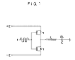
- an inverter including a pair of switching elements Tr1 and Tr2 is connected across a DC power supply having terminals at potentials +E and -E.
- the inverter may be of any well-known construction and generally includes a pair of switching elements Tr1 and Tr2 which are alternately turned on and off at a switching frequency f.
- the switching elements Tr1 and Tr2 may be power transistors or power metal-oxide-semiconductor field-effect transistors (MOSFET) having a withstand voltage of at least 2E, constituting a push-pull inverter.
- MOSFET power metal-oxide-semiconductor field-effect transistors
- the switching elements Tr1 to Tr4 may be constructed from power transistors or ordinary transistors or MOSFET's.
- a pair of complementary P- and N-channel power MOSFET'S are preferably selected for switching elements Tr1 and Tr2.
- Commercially available examples of the power MOSFET of the enhancement mode (or normally off mode) are "2SK310" and "2SJ117” manufactured by Hitachi, Ltd.
- the inverter in the form of paired switching elements Tr1 and Tr2 is connected to an electroluminescent (EL) element having a capacitance C, which is in turn grounded.
- EL electroluminescent
- An inductor in the form of a coil having an inductance L is connected between the inverter and the EL element.
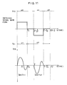
- the EL element when a load is applied to the EL element, the EL element receives a voltage V and a current I as shown in FIG. 2 provided that the resistance (R) component of the circuit is negligibly small.
- the load current I varies over an amplitude of ⁇ CE/ ⁇ LC for a period of ⁇ 0 with a phase shift due to the presence of the coil L.
- the energy loss is then very low though not zero due to the presence of an R component or the like.
- no or little current flows across the inverter circuit for the rise or fall duration of switching operation of switching elements Tr1 and Tr2, resulting in a minimal switching energy loss.
- the coil should have a core having a high magnetic flux permeability at frequency f.
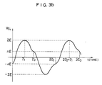
- Tr1 when a load is applied across the EL element, one of the switching elements in the switching section or inverter, for example, Tr1 produces a voltage V DS and a current I DS between the drain and the source as shown in FIG. 3a. Then the EL element receives a voltage V EL as shown in FIG. 3b.
- the voltage V DS that the first switching element Tr1 produces is a rectangular pulse voltage having a height of 2E between ⁇ 0 and 2 ⁇ 0.
- the coil L acts to introduce a phase shift to current I DS such that in a time duration between 0 and ⁇ 1, electric charge flows as a forward current flow a to accumulate in the EL element for a time duration between 0 and ⁇ 0, and returns as a reverse current flow b for a time duration between ⁇ 1 and ⁇ 0.
- the reverse current flow b is shown as a shaded region of I DS in FIG. 3a and the corresponding power or charge is recovered to the same power supply terminal as a surplus power.
- the voltage V EL across the EL element does not have a symmetric waveform as shown in FIG. 2, but a waveform vertically shifted by ⁇ E as shown in FIG. 3b. This means that a charge of ⁇ E ⁇ C cannot be fed back due to light emission of the EL element, dielectric loss and the like.
- the operating system of the invention is designed to carry out synchronous switching at a time constant ⁇ 0 with the capacitor C in FIG. 4 considered to be an EL element or a bipolar capacitor (to be described later) and the switch S considered to be one of the switching elements of the inverter. That is, the operating system of the invention utilizes the oscillatory or transient phenomenon of the LCR circuit. A stable steady state is established in the operating circuit by alternately switching the transient phenomenon occurring when the power supply is +E as shown in FIG. 4 and the transient phenomenon occurring when the power supply is -E, though not shown, in synchronization with the time constant ⁇ 0.
- a resistance equivalent component in the operating circuit corresponding to R of an LCR circuit includes a resistance in the circuit, a magnetic flux loss, DC resistance, and magnetic flux saturation of the coil, a dielectric loss and luminous exitance of the EL element, and the like. Smaller the R equivalent component, the more the reverse current flow or the larger the amount of charge is fed back. If the R equivalent component were zero, an ideal state would be achieved as described in conjunction with FIG. 2.
- the operating circuit of the present invention switches the power supply voltage between +E and -E.
- any conventional well-known methods may be employed, for example, the switching frequency f is adjusted so as to provide synchronization with ⁇ 0. This needs a careful adjustment because if the switching frequency f were wrongly adjusted for synchronization with ⁇ 1, then there would result a very unstable circuit which can cause a failure of the EL element.
- the charge accumulated in the EL element is recovered to the same power supply terminal under the impetus of the coil while minimizing a loss or diversion to the other power supply terminal, thereby improving power efficiency.
- switching elements typically power MOSFET's conduct current flow not only in the drain-to-source direction, but also substantially equally in the source-to-drain direction insofar as the channel is open.
- switching elements having the diode characteristic of allowing only drain-to-source current flow for example, power transistors are used, two groups of diodes D11, D12, D13, D14 and D21, D22, D23, D24 may be arranged as shown in FIG. 7. With this arrangement, both forward and reverse currents flow the switching elements only in a collector-to-emitter or emitter-to-collector direction.
- the DC power supply used in the invention is not particularly limited.
- the use of a secondary battery or solar battery as the power supply is advantageous for power saving.
- direct recharging of the secondary battery with the reverse current flow reduces the battery lifetime and is sometimes difficult for some batteries.
- diodes D1 and D2 are inserted between the power supply terminals +E and -E and the switching elements Tr1 and Tr2, respectively, and capacitors C1 and C1 are connected to the D1-Tr1 and the D2-Tr2 connections, respectively, as shown in FIG. 8.
- FIG. 9 An alternative arrangement is shown in FIG. 9.
- a second inverter is added to the circuit which includes switching elements Tr3 and Tr4 adapted to switch at the same frequency f and close at the time of reverse current flow. It is also effective to further provide coils L3 and L3 between the second inverter and the power supply as phase control inductors because the coils prevent accumulation of charges from the power supply to the capacitors Cl during supply of charges to the EL element or reverse flow of charges from the EL element, considerably reducing the power loss.
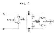
- FIG. 10 A still further arrangement is shown in FIG. 10 which uses a single coil.
- a coil L3 is connected at one end to the aft end of the second inverter consisting of switching elements Tr3 and Tr4 connected to the power supply terminals and at the other end to the connection between diodes D1 and D2.
- the arrangement is such that Tr3 is closed when Tr1 is opened and Tr3 is opened when Tr1 is closed.
- the switching elements Tr1, Tr2, Tr3, and Tr4 open and close as follows. Switching element 0 - ⁇ 0 ⁇ 0 - 2 ⁇ 0 Tr1 Open Close Tr2 Close Open Tr3 Close Open Tr4 Open Close
- inductance L3 and capacitance C1 may also be selected to be approximate values enabling f ⁇ 1/2 ⁇ L3C1 .
- the energy loss is minimized to approximately zero by such a choice.
- the EL elements When it is desired to connect a plurality of EL elements to a direct current supply, the EL elements may be connected in parallel to the output end of the coil L.
- the dynamism that charges accumulated in the EL element are fed back as reverse current flow depends on the capacitances of EL element and capacitors, the inductance of inductor, the frequency and waveform of switching signal. These three parameters must be properly selected before the EL element can be operated by the operating circuit of the invention. Selection of the parameters is not particularly limited and may be carried out by any desired method, but preferably by the following methods because of ease of operation.
- the first method of setting duty ratio is suitable for operating an EL element of a small area at a relatively low frequency without increasing the inductance of the coil.
- FIG. 11 shows the switching signal waveform and drain-to-source current I DS for a fixed frequency f and a duty ratio ⁇ 0/ ⁇ set to less than unity (1).
- This method allows one to adjust and determine the switching frequency and duty ratio while observing the current and voltage waveforms between the drain and the source of one of the switching elements of the inverter on a suitable display such as an oscilloscope. More particularly, the switching frequency and duty ratio are adjusted and determined by manipulating an adjustment volume associated with the oscillatory circuit.
- FIG. 12 shows a circuit for an automatic setting system wherein the current mode will automatically follow a setting of frequency f.
- the circuit includes a charge-up path for forward current flow from the power supply to the EL element and a feedback path for reverse current flow, separately provided between the power supply and the inductor. Both the paths have incorporated therein a charging inverter including switching elements Tr1 and Tr2 and a feedback inverter including switching elements Tr3 and Tr4, and diodes D1, D2, D3, and D4 for separating the paths.
- the charging and feedback inverters are turned on and off with signals having frequencies f2 and f1 matched with the EL operating frequency f.
- This circuit functions such that a charge from the power supply positive terminal +E is accumulated in the EL element as a forward current flow through Tr1 and then fed back as a reverse current flow through Tr3. Similarly, a charge from the power supply negative terminal -E is accumulated in the EL element as a forward current flow through Tr2 and then fed back as a reverse current flow through Tr4. If frequencies f1 and f2 are forward synchronous pulses, a choice is made such that transistors Tr1 and Tr3 are of the same channel type, transistors Tr2 and Tr4 are of the same channel type, and Tr1 and Tr2 and Tr3 and Tr4 are pairs of complementary transistors of different channel types.
- transistors Tr1 and Tr3 are of different channel types
- transistors Tr2 and Tr4 are of different channel types
- Tr1 and Tr2 and Tr3 and Tr4 are pairs of complementary transistors of different channel types.
- the signal wave for switching the transistors Tr3 and Tr4 of the feedback inverter is of rectangular waveform and has a frequency f1 equal to the EL operating frequency f.
- the signal wave of frequency fl may have a pulse duration duty ratio of at least ⁇ 0/ ⁇ though it is generally selected to be a fixed value. In the illustrated embodiment, the duty ratio is equal to 1.
- the signal wave for switching the transistors Tr1 and Tr2 of the charging inverter is of rectangular waveform and has a frequency f2 equal to the EL operating frequency f.
- the signal wave of frequency f2 may have a pulse duration ⁇ 2 having a duty ratio ⁇ 2/ ⁇ which may be either fixed or variable, though a certain restraint is imposed as will be described later.
- the duty ratio ⁇ 2/ ⁇ is generally up to ⁇ 0/ ⁇ , preferably in the range of from ⁇ 1/ ⁇ to ⁇ 0/ ⁇ . It will be understood that the frequency and duty ratio are arbitrary and may be suitably determined insofar as the above-mentioned requirements are met.
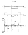
- FIG. 13 is a diagram showing the waveforms of drain-source current flows I1 DS and I3 DS through transistors Tr1 and Tr3 along with the signal waves having frequencies f1 and f2.
- curves in broken lines show the waveforms of drain- source current flows I2 DS and I4 DS through transistors Tr2 and Tr4 associated with the power supply negative terminal -E.
- time constants ⁇ 1 and ⁇ 0 are variables determined as a function of the capacitance, inductance, and resistance of the circuit.
- the value of pulse duration ⁇ 2 need not be identical to the value of ⁇ 1 or ⁇ 0 as seen from FIG. 13, though ⁇ 2 ⁇ ⁇ 0 is necessary as previously described. If ⁇ 2 > ⁇ 0, then the charge once fed back to the power supply terminal is undesirably accumulated again in the EL element through Tr1.
- Another preferred condition is ⁇ 2 ⁇ ⁇ 1 because a noticeable switching energy loss occurs under a condition: ⁇ 2 ⁇ ⁇ 1.
- This operating circuit enables automatic feedback of reverse current flow even if the signal waves of frequencies f1 and f2 are once set and thereafter kept fixed insofar as the condition: ⁇ 2 ⁇ ⁇ 0 is met. This allows the reverse current feed back mode to be automatically followed even when the value of ⁇ 0 has changed due to a change with time of the capacitance of the EL element which is a drawback of the EL element.
- the EL element lowers its capacitance as it is operated for an extended period, say several years.
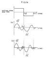
- the value of ⁇ 0 which was equal to the value of ⁇ of switching frequency f at the time of initial setting as shown in a middle section of FIG. 14 decreases so that ⁇ 0 is out of timing with ⁇ as shown in a lower section of FIG. 14.
- I DS is a drain-source current flow at the time of initial setting
- I′ DS is a drain-source current flow after a change with time of the EL element capacitance
- (+) and (-) designate that the associated current flows are on the positive and negative sides of the power supply, respectively.
- a recharging current flow corresponding to a shaded area in the lower section of FIG. 14 generates, resulting in a reduced EL operating efficiency.
- the automatic setting arrangement as illustrated in FIG. 12 essentially eliminates the switching loss and occurrence of a re-charging current flow due to a capaci. tance change with time of the EL element insofar as the condition: ⁇ 1 ⁇ ⁇ 2 ⁇ ⁇ 0 is met.
- FIG. 15 A modification of the circuit of FIG. 12 is shown in FIG. 15 wherein diodes are inserted between the power supply terminals and the switching elements Tr1 and Tr2 of the charging inverter, and capacitors C1, C1 are provided for buffering the reverse current flows for the same reason as previously described.
- the provision of a second inverter or a phase control inductor as shown in FIG. 9 or 10 can further reduce the power loss.
- bypass channels for reverse current flows are formed by connecting diodes D3 and D4 in parallel with the switching elements Tr1 and Tr2 of the inverter, respectively, whereby the reverse current flow mode is automatically locked within a certain range of parameter settings.
- the circuit of FIG. 20 becomes equivalent to that of FIG. 21 when switching elements Tr1 and Tr2 in FIG. 20 also have a diode function like transistors do. These arrangements correspond to the circuit arrangement of FIG. 12 with switching elements Tr3 and Tr4 omitted.
- the operation of the circuit of FIG. 21 is now described for better understanding.
- the switching element Tr1 should be closed at the point of time when the reverse current flow has been recovered to the positive terminal side.
- the second switching element Tr2 should be kept closed until the positive reverse current flow has been recovered to the positive terminal side.
- FIG. 22 shows the waveform of current flow through an LCR circuit given by the L, C and R component of the circuit of FIG. 21 when second switching element Tr2 of FIG. 21 is opened and the waveform of the frequency f switching signal of the inverter.
- reverse current flow locking is automatically accomplished because of ⁇ 1 ⁇ ⁇ 2 ⁇ ⁇ 0 and ⁇ 0 ⁇ ⁇ . That is, the illustrated arrangement can successfully achieve automatic locking of reverse current flow within the range where the conditions: ⁇ 1 ⁇ ⁇ 2 ⁇ ⁇ 0 and ⁇ 0 ⁇ ⁇ are met.
- Imin and Imax respectively designate the waveforms of current flow corresponding to the minimum and maximum areas of an EL element involved in the circuit arrangement wherein reverse current flow is automatically locked.
- the present system can adjust luminance by varying the frequency within the range of EL element minimum to maximum area ratio of 1 : 2.25 for the same fixed L value.
- a still another system capable of automatic follow-up of frequency f is contemplated wherein the frequency f is automatically adjusted to be equal to 1/2 ⁇ 0 in accordance with a change of ⁇ 0, that is, switching elements are automatically opened or closed when the reverse current flow has been fed back.
- a system capable of automatic follow-up of pulse duration duty ratio is also contemplated wherein the frequency f is left variable, and the switching elements are automatically closed when the reverse current flow has been fed back.
- These circuits may be established by using those switching elements which are automatically turned off when current is available no longer, typically triacs, with a modification to the illustrated circuit embodiments.
- an oscillatory circuit may be modified such that the frequency or pulse duration duty ratio of the switching signal to the inverter will follow in synchronization when the reverse current flow has been fed back.
- a power supply of the dual mode providing potentials of ⁇ E volts is necessary and the other end of the EL element is connected to an intermediate or zero potential terminal, that is, grounded.
- a primary power supply of the single mode it must be converted into a power supply of the dual mode allowing connection of an intermediate potential terminal before it can be used as the input power supply in the operating circuit of the invention.
- Any conventional well-known method may be used to convert a power supply of the single mode into a power supply of the dual mode. Some suitable methods are described below.
- a first method is to use a DC-DC converter of the dual mode with an advantage that voltage can be stepped up and down at the same time.
- the potential of 2E volt may be divided into ⁇ E volt and intermediate potentials using two capacitors C4, C4 having an equal capacitance.
- the arrangement is shown in FIG. 16 wherein a first capacitor C4 and a second capacitor C4 are connected across the primary power supply of 2E.
- a terminal 1 between the power supply positive terminal and first capacitor C4 produces an output of +E volt and a terminal 3 between the power supply negative terminal and second capacitor C4 produces an output of -E volt with respect to an intermediate terminal 2 at the connection between first and second capacitors C4 and C4.
- the terminals 1 and 3 are used as input terminals for the inverter while the intermediate terminal 2 is used as the ground terminal for the EL element.
- a DC-DC converter of the dual mode as previously described may be used. It is also possible to use a DC-DC converter of the single mode to convert the potential of e volt into a potential of 2E volt, which can then be divided into ⁇ E volt and intermediate potentials using a capacitor connection as shown in FIG. 16.
- reverse current controlling diodes D1 and D2 are inserted between the primary power supply or the DC-DC converter and the potential dividing capacitors C4 because the capacitors C4 can then also serve to buffer reverse flow power.
- the second aspect is the same in principle as the first aspect in that a reverse current flow is available.
- the second aspect is made by taking into account that the DC power supply potentials of ⁇ E are stepped up to apply an AC load to the EL element.
- Necessary replacements are made to the embodiment of the first aspect.
- the EL element is replaced by a bipolar capacitor, the inductor or coil is replaced by a transformer having primary and secondary windings, and the EL element is connected to the transformer whereby the EL element is operated with an AC power available at the transformer secondary winding.
- FIGS. 17 and 18 Two preferred embodiments are shown in FIGS. 17 and 18.
- power supply terminals having potentials of +E and -E are connected to an inverter consisting of switching elements Tr1 and Tr2 as in the first aspect.
- the output of the inverter is connected to a transformer T having primary and secondary windings having inductances L1 and L2.
- the secondary winding L2 is connected across an EL element having a capacitance C.
- the primary winding L1 is connected to a bipolar capacitor having a capacitance C3.
- FIG. 18 is a modification of FIG. 17.
- FIG. 19 is a further modification of FIG. 18 wherein a coil L′ is added as a compensating inductor.
- the inductor L or transformer T between the inverter and the EL element or bipolar capacitor C3 causes phase and period shifts between loading current and voltage, no or little current flows across the circuit at the instant when the switching elements of the inverter are opened and closed, eliminating or minimizing the switching energy loss by the switching elements such as power transistors and power MOSFET.
- a substantial portion of the charge accumulated in the EL element is recovered as reverse current flow to the power supply terminal from which the charge is delivered, by virtue of the inductor or transformer, minimizing any loss to the other terminal and thus resulting in significantly increased power efficiency.
- the EL element can generate an increased amount of light at an increased luminance.
- the amount of heat that the switching elements such as power transistors and power MOSFET generate is significantly reduced with an increased degree of safety, eliminating the need for heat dissipating means.
- Table 1 shows the luminous intensity of each EL panel and the temperature of a heat sink associated with each power MOSFET having an area of 150 cm2 which is indicative of the amount of heat each power MOSFET generated.
- Table 1 also shows the results obtained when an inductance L of 50 mH was connected between the inverter and the parallel connected EL panels according to the present invention.
- Table 1 Luminous intensity (surface illuminance) Temperature of heat sink Comparison 130 lx 115°C Invention 500 lx 42°C
- the present invention provides significant improvements in luminance and power consumption as compared with the prior art system.
- the present invention accomplishes provides significant improvements in both luminance and power consumption over the entire range of varying voltage though the same frequency and effective voltage are used. That is, luminance is increased and power consumption is reduced.
- luminance is increased and power consumption is reduced.
- the benefit that a luminance increase and a power saving are achieved at the same time will be better understood from a quantitative aspect by comparing the power consumption required for providing the same luminance.
- the prior art needs a power consumption of 27.58 m/mVA (Table 2) and the invention needs a power consumption of 6.88 m/mVA (Table 3) which is about 1/4 of the power consumption of the prior art.
Landscapes
- Physics & Mathematics (AREA)
- Engineering & Computer Science (AREA)
- Microelectronics & Electronic Packaging (AREA)
- Optics & Photonics (AREA)
- Inverter Devices (AREA)
- Electroluminescent Light Sources (AREA)
- Dc-Dc Converters (AREA)
Abstract
Description
- This invention relates to an EL operating power supply circuit.
- Electroluminescent (EL) elements or panels are widely used as EL displays and background light for liquid crystal displays.
- The EL element is predominantly a capacitance load when considered as a load, and generally requires AC voltage application for operation. The luminance and corresponding surface illuminance of the EL element largely depends on both the voltage and frequency of alternating current applied thereto. In order that the EL element generate more light, the effective or root-mean-square value and/or the frequency of applied voltage is increased.
- No particular measure is required when the EL element is operated directly with an ordinary AC power supply, for example, having an effective value of 100 volts and a frequency of 50 or 60 Hz. To derive more light from the EL element, however, it is necessary to increase the frequency and to increase the voltage within the withstand voltage of the EL element. When the EL element is operated directly with an ordinary 100-volt AC power supply, the maximum voltage applied to the EL element has a peak magnitude of 140 volts (a peak-to-peak magnitude of 280 volts). Most EL elements have a rated withstand voltage of approximately 210 volts (a peak-to-peak value of 420 volts). The permissible frequency has a practical upper limit of approximately 400 Hz in view of the lifetime of EL element.
- The frequency of voltage applied to an EL element may be increased by once rectifying an AC power to form a DC power supply of about ±140 volts, and alternately opening the positive/negative power supply circuit at the desired frequency f by means of a push-pull circuit, thereby applying AC voltage at the frequency f to the EL element. Generally, power transistors and power MOSFET's are used as the switching elements of the push-pull circuit. An energy loss of such power transistors and power MOSFET's upon switching gives rise to problems that a relatively large heat sink is necessary, a considerable energy loss occurs, and the site and manner of locating such transistors must be carefully taken into account.
- Therefore, a primary object of the invention is to provide a power supply circuit for operating an EL element which essentially eliminates energy loss, recovers surplus electric charge in the EL element as reverse current flow to the power supply side, and thus increases energy efficiency.
- According to a first aspect of the present invention, there is provided an EL operating power supply circuit comprising a DC power supply, an inverter connected across the power supply for producing an AC voltage at an output thereof, electroluminescent (EL) means connected to the output of the inverter, and an inductor inserted between the inverter and the electroluminescent means wherein the AC voltage is applied from the inverter through the inductor to the electroluminescent means to emit light.
- According to a second aspect of the present invention, there is provided an EL operating power supply circuit comprising a DC power supply, an inverter connected across the power supply for changing the DC power into an AC power at an output thereof, and a transformer connected to the output of the inverter having primary and secondary windings, a bipolar capacitor connected to the transformer, and electroluminescent (EL) means connected to the transformer such that an AC output power available on the transformer secondary winding is applied to the electroluminescent means to emit light.
- Several preferred embodiments common to both the EL operating circuits of the first and second aspects are described below.
- The electroluminescent means may be an electroluminescent element or an array of parallel connected electroluminescent elements.
- A bipolar capacitor may be connected parallel to the electroluminescent means.
- The inductance of the inductor or transformer reduces the current during switching operation of the inverter, and a charge accumulated in the electroluminescent means and/or the bipolar capacitor through the inverter and the inductor or transformer is recovered to the power supply side as a reverse current flow.
- A buffering capacitor may be connected between the DC power supply and the inverter.
- A second inverter may be connected between the DC power supply and the first inverter, the second inverter performing opposite switching operation to the first inverter.
- A phase controlling coil may be connected between the DC power supply and the second inverter and/or between the first and second inverters.
- The first inverter may be adapted to receive a switching signal wherein the frequency and/or pulse duration duty ratio of the switching signal can be set in a variable manner.
- The inverter may include a charging inverter section and a feedback inverter section. The charging and feedback inverter sections may be driven by a switching signal having the same frequency and the same rise. The feedback inverter section has a larger pulse duration duty ratio than the charging inverter section.
- The inverter may include at least a pair of switching elements, and first diodes each may be connected in parallel with one of the switching elements for forming a bypass channel for feeding back the reverse current flow. Second diodes each may be provided in forward series connection with one of the switching elements inside the inverter channel bypassed by the reverse current flow bypass channel.
- The above and other objects, features, and advantages of the present invention will be better understood from the following description taken in conjunction with the accompanying drawings, in which:
- FIGS. 1, 6-10, 12, 15, 17-21 are diagrams illustrating EL operating power supply circuits according to different embodiments of the invention;
- FIGS. 2, 3a and 3b are diagrams showing changes with time of voltage V and current I applied to an EL element, drain-source voltage VDS and current IDS, and voltage VEL actually applied to the EL element, respectively;
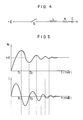
- FIG. 4 schematically illustrates an LCR series circuit;
- FIG. 5 is a diagram showing changes with time of voltage Vc and current I in the capacitor C in the LCR series circuit of FIG. 4;
- FIG. 11 is a diagram showing changes with time of switching signal waveform and drain-source current IDS with the pulse duration duty ratio set to be less than 1;
- FIG. 13 is a diagram showing changes with time of waveforms of switching signal waves having frequencies f1 and f2 and drain-source currents I¹DS, I²DS, I³DS, and I⁴DS, when a reverse feedback current flow mode automatic setting system according to the invention is used;
- FIG. 14 is a diagram showing changes with time of drain-source currents I(+) DS and I(-) DS available at the time of initial setting and drain-source currents I′(+) DS and I′(-) DS after the EL element has changed its capacitance, when an automatic setting system is not used;
- FIG. 16 is a diagram showing one exemplary circuit for converting a single mode power supply voltage into a double mode output voltage;
- FIGS. 22 and 23 are diagrams showing changes with time of the waveform of switching signal having frequency f and current according to different automatic setting systems of the invention.
- Like parts are designated by the same reference numerals throughout the figures.
- Referring to FIG. 1, there is illustrated an EL operating power supply circuit according to the first aspect of the present invention. It is to be noted that throughout the specification, a capacitor having a capacitance C is often referred to as capacitor C, and an inductor or coil having an inductance L referred to as inductor or coil L for brevity of description.
- In the power supply circuit of the invention, an inverter including a pair of switching elements Tr1 and Tr2 is connected across a DC power supply having terminals at potentials +E and -E. The inverter may be of any well-known construction and generally includes a pair of switching elements Tr1 and Tr2 which are alternately turned on and off at a switching frequency f. The switching elements Tr1 and Tr2 may be power transistors or power metal-oxide-semiconductor field-effect transistors (MOSFET) having a withstand voltage of at least 2E, constituting a push-pull inverter. In the illustrated embodiment, power MOSFET's are used as the switching elements Tr1 and Tr2 as well as Tr3 and Tr4 which will be described later. Alternatively, the switching elements Tr1 to Tr4 may be constructed from power transistors or ordinary transistors or MOSFET's.
- When power MOSFET's are used, a pair of complementary P- and N-channel power MOSFET'S are preferably selected for switching elements Tr1 and Tr2. Commercially available examples of the power MOSFET of the enhancement mode (or normally off mode) are "2SK310" and "2SJ117" manufactured by Hitachi, Ltd.
- The inverter in the form of paired switching elements Tr1 and Tr2 is connected to an electroluminescent (EL) element having a capacitance C, which is in turn grounded.
- An inductor in the form of a coil having an inductance L is connected between the inverter and the EL element. In an ideal state wherein the resistance (R) component or R equivalent component of the circuit is negligibly small, the relation between L and C is given by the equation:
f = 1/4π√LC
wherein π is the circular constant. Since the EL element has a known capacitance C and the frequency f is given by the desired luminance, L may be determined from the given values of f and C. Since f is generally in the range of 50 Hz to 600 Hz and C is of the order of 0.1 µF to 10 µF, then L is of the order of 30 mH to 10 H. - With such a circuit arrangement, when a load is applied to the EL element, the EL element receives a voltage V and a current I as shown in FIG. 2 provided that the resistance (R) component of the circuit is negligibly small. The load voltage V varies over an amplitude of ±2E for a period of 2τ₀ wherein τ₀ = 1/2f = 2π√
LC . The load current I varies over an amplitude of ±CE/√LC for a period of τ₀ with a phase shift due to the presence of the coil L. As a consequence, little current flows across the circuit at the instant of switching operation of switching elements Tr1 and Tr2. The energy loss is then very low though not zero due to the presence of an R component or the like. Thus no or little current flows across the inverter circuit for the rise or fall duration of switching operation of switching elements Tr1 and Tr2, resulting in a minimal switching energy loss. - As understood from the foregoing, the coil or inductor should have an inductance L which can meet the equation: f = 1/4π√
LC and at the same time, is higher than the value given from the equation: Imax = CE/√LC for the maximum permissible current for the coil. The coil should have a core having a high magnetic flux permeability at frequency f. - With the above-described arrangement, when a load is applied across the EL element, one of the switching elements in the switching section or inverter, for example, Tr1 produces a voltage VDS and a current IDS between the drain and the source as shown in FIG. 3a. Then the EL element receives a voltage VEL as shown in FIG. 3b.
- More particularly, the voltage VDS that the first switching element Tr1 produces is a rectangular pulse voltage having a height of 2E between τ₀ and 2τ₀. The coil L acts to introduce a phase shift to current IDS such that in a time duration between 0 and τ₁, electric charge flows as a forward current flow a to accumulate in the EL element for a time duration between 0 and τ₀, and returns as a reverse current flow b for a time duration between τ₁ and τ₀. The reverse current flow b is shown as a shaded region of IDS in FIG. 3a and the corresponding power or charge is recovered to the same power supply terminal as a surplus power.
- In the foregoing description, if it is assumed that the resistance (R) component is zero and that the energy required for the EL element to emit light is zero, then the regions a and b in FIG. 3a have an equal area, presenting perpetual motion. Of course, this cannot happen. In practice, the power is consumed by resistance equivalent components of the circuit, that is, a resistance component of the circuit, a magnetic field loss in the inductor (L), light emitting energy of the EL element and the like, resulting in a > b as illustrated in FIG. 3a. In fact, b is substantially smaller than a.
- The voltage VEL across the EL element does not have a symmetric waveform as shown in FIG. 2, but a waveform vertically shifted by ±ΔE as shown in FIG. 3b. This means that a charge of ΔE·C cannot be fed back due to light emission of the EL element, dielectric loss and the like.
- Nevertheless, important is the fact that a power corresponding to area b is recovered to the same power supply terminal, contributing to an improvement in power efficiency. In the prior art electroluminescent system, a power corresponding to this reverse flow component is discarded to the counter terminal, that is, the other power supply terminal as a transmission loss rather than a switching loss.
- The principle of power recovery is described in further detail by referring to an oscillatory inductance-capacitance-resistance (LCR) circuit as shown in FIG. 4.
- After closing a switch S in the serial LCR circuit of FIG. 4, voltage Vc across a capacitor C and current I through the circuit change with time as shown in FIG. 5 as is well known as the dynamic transient phenomenon of an LCR circuit. In FIG. 5, τ₁ and τ₀ are time constants which are determined from the values of L, C and R.
- The operating system of the invention is designed to carry out synchronous switching at a time constant τ₀ with the capacitor C in FIG. 4 considered to be an EL element or a bipolar capacitor (to be described later) and the switch S considered to be one of the switching elements of the inverter. That is, the operating system of the invention utilizes the oscillatory or transient phenomenon of the LCR circuit. A stable steady state is established in the operating circuit by alternately switching the transient phenomenon occurring when the power supply is +E as shown in FIG. 4 and the transient phenomenon occurring when the power supply is -E, though not shown, in synchronization with the time constant τ₀.
- It is to be noted that a oscillatory phenomenon as shown in FIG. 5 does not occur in the LCR circuit when the resistance R exceeds a certain value. If the operating circuit of the invention has a resistance equivalent component in excess of a certain value, no reverse flow of charge does occur.
- A resistance equivalent component in the operating circuit corresponding to R of an LCR circuit includes a resistance in the circuit, a magnetic flux loss, DC resistance, and magnetic flux saturation of the coil, a dielectric loss and luminous exitance of the EL element, and the like. Smaller the R equivalent component, the more the reverse current flow or the larger the amount of charge is fed back. If the R equivalent component were zero, an ideal state would be achieved as described in conjunction with FIG. 2.
- For the construction of a operating circuit, a choice of the coil is important and it should be carefully chosen so as to meet the above-mentioned requirements. Also switching elements should desirably have a reduced on-state resistance.
- The operating circuit of the present invention switches the power supply voltage between +E and -E. To this end, any conventional well-known methods may be employed, for example, the switching frequency f is adjusted so as to provide synchronization with τ₀. This needs a careful adjustment because if the switching frequency f were wrongly adjusted for synchronization with τ₁, then there would result a very unstable circuit which can cause a failure of the EL element.
- According to the present invention, the charge accumulated in the EL element is recovered to the same power supply terminal under the impetus of the coil while minimizing a loss or diversion to the other power supply terminal, thereby improving power efficiency.
- It is to be noted that if it is desired to have a lower inductance than the value of L determined from the equation: f = 1/4π√
LC for the ideal state circuit, a bipolar capacitor Co′ may be connected in parallel to the EL element as shown in FIG. 6. Then the inductance L of the coil may be set to a value calculated from the equation using C given as the sum of the capacitance Co′ of this dummy capacitor and the capacitance Co of the EL element. In this case, however, the current value, especially the maximum current value Imax = CE/√LC through the coil L is also increased as the inductance is reduced. The diameter of a wire used for winding the coil must be increased in proportion to a reduction of inductance. - Most switching elements, typically power MOSFET's conduct current flow not only in the drain-to-source direction, but also substantially equally in the source-to-drain direction insofar as the channel is open. When switching elements having the diode characteristic of allowing only drain-to-source current flow, for example, power transistors are used, two groups of diodes D11, D12, D13, D14 and D21, D22, D23, D24 may be arranged as shown in FIG. 7. With this arrangement, both forward and reverse currents flow the switching elements only in a collector-to-emitter or emitter-to-collector direction.
- The DC power supply used in the invention is not particularly limited. The use of a secondary battery or solar battery as the power supply is advantageous for power saving. However, direct recharging of the secondary battery with the reverse current flow reduces the battery lifetime and is sometimes difficult for some batteries.
- Therefore, when it is desired to use a battery as the power supply, diodes D1 and D2 are inserted between the power supply terminals +E and -E and the switching elements Tr1 and Tr2, respectively, and capacitors C1 and C1 are connected to the D1-Tr1 and the D2-Tr2 connections, respectively, as shown in FIG. 8.
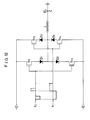
- An alternative arrangement is shown in FIG. 9. In addition to diodes D1 and D2 and capacitors C1 and C1 connected as in the immediately preceding embodiment, a second inverter is added to the circuit which includes switching elements Tr3 and Tr4 adapted to switch at the same frequency f and close at the time of reverse current flow. It is also effective to further provide coils L3 and L3 between the second inverter and the power supply as phase control inductors because the coils prevent accumulation of charges from the power supply to the capacitors Cl during supply of charges to the EL element or reverse flow of charges from the EL element, considerably reducing the power loss.
- A still further arrangement is shown in FIG. 10 which uses a single coil. A coil L3 is connected at one end to the aft end of the second inverter consisting of switching elements Tr3 and Tr4 connected to the power supply terminals and at the other end to the connection between diodes D1 and D2.
- In the embodiments of FIGS. 9 and 10, the switching frequencies for the first and second inverters are equal, that is, f1 = f2. The arrangement is such that Tr3 is closed when Tr1 is opened and Tr3 is opened when Tr1 is closed. More particularly, the switching elements Tr1, Tr2, Tr3, and Tr4 open and close as follows.
Switching element 0 - τ₀ τ₀ - 2τ₀ Tr1 Open Close Tr2 Close Open Tr3 Close Open Tr4 Open Close - The equation: f = 1/4π√
LC for the ideal state circuit applies to these embodiments provided that C is given by 1/C = 1/C1 + 1/C2 wherein C1 is the capacitance of the capacitor and C2 is the capacitance of the EL element. It is permissible to assume C ≈ C2 in the event of C1 » C2. - Since the coil L3 is inserted for the purpose of avoiding the switching energy loss in switching elements Tr3 and Tr4, inductance L3 and capacitance C1 may also be selected to be approximate values enabling f ≧ 1/2π√
L3C1 . The energy loss is minimized to approximately zero by such a choice. - When it is desired to connect a plurality of EL elements to a direct current supply, the EL elements may be connected in parallel to the output end of the coil L.
- In the operating circuit of the invention used to operate the EL element, the dynamism that charges accumulated in the EL element are fed back as reverse current flow depends on the capacitances of EL element and capacitors, the inductance of inductor, the frequency and waveform of switching signal. These three parameters must be properly selected before the EL element can be operated by the operating circuit of the invention. Selection of the parameters is not particularly limited and may be carried out by any desired method, but preferably by the following methods because of ease of operation.
- (1) A first method uses a fixed switching frequency f (τ) of the inverter and a variable pulse duration duty ratio (ratio of open duration τ₀ of a switching element to half period τ, τ₀/τ) to thereby determine the duty ratio.
- (2) A second method uses a fixed duty ratio and a variable switching frequency f to thereby determine the switching frequency.
- (3) A third method uses both a variable switching frequency f and a variable duty ratio to thereby determine both the values.
- These methods are advantageous in that they can accommodate for any change of the luminance requirement and replacement to an EL element having a different capacitance without changing the inductor.
- In particular, the first method of setting duty ratio is suitable for operating an EL element of a small area at a relatively low frequency without increasing the inductance of the coil. FIG. 11 shows the switching signal waveform and drain-to-source current IDS for a fixed frequency f and a duty ratio τ₀/τ set to less than unity (1). This method allows one to adjust and determine the switching frequency and duty ratio while observing the current and voltage waveforms between the drain and the source of one of the switching elements of the inverter on a suitable display such as an oscilloscope. More particularly, the switching frequency and duty ratio are adjusted and determined by manipulating an adjustment volume associated with the oscillatory circuit.
- Next, a further preferred embodiment of the EL operating circuit of the invention is described wherein synchronized feedback of reverse current flow is automatically accomplished without resorting to manual operation such as volume adjustment.
- FIG. 12 shows a circuit for an automatic setting system wherein the current mode will automatically follow a setting of frequency f. The circuit includes a charge-up path for forward current flow from the power supply to the EL element and a feedback path for reverse current flow, separately provided between the power supply and the inductor. Both the paths have incorporated therein a charging inverter including switching elements Tr1 and Tr2 and a feedback inverter including switching elements Tr3 and Tr4, and diodes D1, D2, D3, and D4 for separating the paths. The charging and feedback inverters are turned on and off with signals having frequencies f2 and f1 matched with the EL operating frequency f.
- This circuit functions such that a charge from the power supply positive terminal +E is accumulated in the EL element as a forward current flow through Tr1 and then fed back as a reverse current flow through Tr3. Similarly, a charge from the power supply negative terminal -E is accumulated in the EL element as a forward current flow through Tr2 and then fed back as a reverse current flow through Tr4. If frequencies f1 and f2 are forward synchronous pulses, a choice is made such that transistors Tr1 and Tr3 are of the same channel type, transistors Tr2 and Tr4 are of the same channel type, and Tr1 and Tr2 and Tr3 and Tr4 are pairs of complementary transistors of different channel types. If frequencies f1 and f2 are opposite synchronous pulses, a choice is made such that transistors Tr1 and Tr3 are of different channel types, transistors Tr2 and Tr4 are of different channel types, and Tr1 and Tr2 and Tr3 and Tr4 are pairs of complementary transistors of different channel types.
- The signal wave for switching the transistors Tr3 and Tr4 of the feedback inverter is of rectangular waveform and has a frequency f1 equal to the EL operating frequency f. The signal wave of frequency fl may have a pulse duration duty ratio of at least τ₀/τ though it is generally selected to be a fixed value. In the illustrated embodiment, the duty ratio is equal to 1.
- The signal wave for switching the transistors Tr1 and Tr2 of the charging inverter is of rectangular waveform and has a frequency f2 equal to the EL operating frequency f. The signal wave of frequency f2 may have a pulse duration τ₂ having a duty ratio τ₂/τ which may be either fixed or variable, though a certain restraint is imposed as will be described later. The duty ratio τ₂/τ is generally up to τ₀/τ, preferably in the range of from τ₁/τ to τ₀/τ. It will be understood that the frequency and duty ratio are arbitrary and may be suitably determined insofar as the above-mentioned requirements are met.
- The process of charging and feedback of charges associated with the positive power supply terminal +E is now described by referring to the drain-source current flows I¹DS and I³DS through transistors Tr1 and Tr3 and the signal waves of frequencies f1 and f2. FIG. 13 is a diagram showing the waveforms of drain-source current flows I¹DS and I³DS through transistors Tr1 and Tr3 along with the signal waves having frequencies f1 and f2. In the current waveform section, curves in broken lines show the waveforms of drain- source current flows I²DS and I⁴DS through transistors Tr2 and Tr4 associated with the power supply negative terminal -E.
- In the operating circuit of FIG. 12, time constants τ₁ and τ₀ are variables determined as a function of the capacitance, inductance, and resistance of the circuit. The value of pulse duration τ₂ need not be identical to the value of τ₁ or τ₀ as seen from FIG. 13, though τ₂ ≦ τ₀ is necessary as previously described. If τ₂ > τ₀, then the charge once fed back to the power supply terminal is undesirably accumulated again in the EL element through Tr1. Another preferred condition is τ₂ ≧ τ₁ because a noticeable switching energy loss occurs under a condition: τ₂ < τ₁.
- This operating circuit enables automatic feedback of reverse current flow even if the signal waves of frequencies f1 and f2 are once set and thereafter kept fixed insofar as the condition: τ₂ ≦ τ₀ is met. This allows the reverse current feed back mode to be automatically followed even when the value of τ₀ has changed due to a change with time of the capacitance of the EL element which is a drawback of the EL element.
- The EL element lowers its capacitance as it is operated for an extended period, say several years. Unless the automatic setting mode is used, the value of τ₀ which was equal to the value of τ of switching frequency f at the time of initial setting as shown in a middle section of FIG. 14 decreases so that τ₀ is out of timing with τ as shown in a lower section of FIG. 14. In FIG. 14, IDS is a drain-source current flow at the time of initial setting and I′DS is a drain-source current flow after a change with time of the EL element capacitance, and (+) and (-) designate that the associated current flows are on the positive and negative sides of the power supply, respectively. Then, a recharging current flow corresponding to a shaded area in the lower section of FIG. 14 generates, resulting in a reduced EL operating efficiency.
- The automatic setting arrangement as illustrated in FIG. 12 essentially eliminates the switching loss and occurrence of a re-charging current flow due to a capaci. tance change with time of the EL element insofar as the condition: τ₁ ≦ τ₂ ≦ τ₀ is met.
- A modification of the circuit of FIG. 12 is shown in FIG. 15 wherein diodes are inserted between the power supply terminals and the switching elements Tr1 and Tr2 of the charging inverter, and capacitors C1, C1 are provided for buffering the reverse current flows for the same reason as previously described. The provision of a second inverter or a phase control inductor as shown in FIG. 9 or 10 can further reduce the power loss.
- Another automatic setting method is described wherein the current flow mode is followed by providing reverse current flow bypass channels in the form of diodes in parallel with the switching elements of the inverter.
- This method is enabled by the circuit arrangements shown in FIGS. 20 and 21 in which bypass channels for reverse current flows are formed by connecting diodes D3 and D4 in parallel with the switching elements Tr1 and Tr2 of the inverter, respectively, whereby the reverse current flow mode is automatically locked within a certain range of parameter settings.
- The circuit of FIG. 20 becomes equivalent to that of FIG. 21 when switching elements Tr1 and Tr2 in FIG. 20 also have a diode function like transistors do. These arrangements correspond to the circuit arrangement of FIG. 12 with switching elements Tr3 and Tr4 omitted. The operation of the circuit of FIG. 21 is now described for better understanding. During a time interval when first switching element Tr1 is opened and second switching element Tr2 is closed, positive charges are accumulated in the EL element through diode D1, switching element Tr1 and coil L, and reverse current flow is recovered to the positive terminal through diode D3. The switching element Tr1 should be closed at the point of time when the reverse current flow has been recovered to the positive terminal side. The second switching element Tr2 should be kept closed until the positive reverse current flow has been recovered to the positive terminal side.
- It is now assumed that FIG. 22 shows the waveform of current flow through an LCR circuit given by the L, C and R component of the circuit of FIG. 21 when second switching element Tr2 of FIG. 21 is opened and the waveform of the frequency f switching signal of the inverter. In this case, reverse current flow locking is automatically accomplished because of τ₁ ≦ τ₂ ≦ τ₀ and τ₀ ≦ τ. That is, the illustrated arrangement can successfully achieve automatic locking of reverse current flow within the range where the conditions:
τ₁ ≦ τ₂ ≦ τ₀ and
τ₀ ≦ τ
are met. - It is to be noted that automatic locking of reverse current flow can be achieved under conditions: τ₁ > τ₂ and τ₀ ≦ τ. However, these conditions would produce a switching loss because first switching element Tr1 is closed while the accumulating current is flowing and provide less efficient light emission because insufficient charge is delivered to the EL element.
- Next, the range of an available EL element area is discussed for the circuit arrangement of FIG. 21 wherein the inductance L and switching waveform are fixed.
- It is now assumed that in FIG. 23, for the fixed waveform of switching signal having frequency f and the fixed inductance L, Imin and Imax respectively designate the waveforms of current flow corresponding to the minimum and maximum areas of an EL element involved in the circuit arrangement wherein reverse current flow is automatically locked. Provided that the EL element has capacitances Cmin and Cmax corresponding to Imin and Imax, respectively, and τ₁ : τ₀ = τ′₁ : τ′₀ ≈ 2 : 1 (this time constant ratio was empirically found to be approximately 2 : 1), then
τ₁ : τ′₁ = τ₀ : τ′₀ = 2 : 3 = √Cmin : √Cmax .
Then, Cmin : Cmax = 4 : 9. Since the capacitance C of EL elements is proportional to their area for a group of elements of the same type, the range of an available EL area is given by the ratio of minimum area to maximum area which is equal to 4 : 9 = 1 : 2.25 for the fixed waveform of switching signal having frequency f and the fixed inductance L. - In the event that the open duration τ₂ of the switching waveform is fixed and the frequency f is variable in a range of τ′₀ ≦ τ = 1/2f, that is, f ≦ 1/2τ′₀, the present system can adjust luminance by varying the frequency within the range of EL element minimum to maximum area ratio of 1 : 2.25 for the same fixed L value.
- Though not shown, a still another system capable of automatic follow-up of frequency f is contemplated wherein the frequency f is automatically adjusted to be equal to 1/2τ₀ in accordance with a change of τ₀, that is, switching elements are automatically opened or closed when the reverse current flow has been fed back. Alternatively, a system capable of automatic follow-up of pulse duration duty ratio is also contemplated wherein the frequency f is left variable, and the switching elements are automatically closed when the reverse current flow has been fed back. These circuits may be established by using those switching elements which are automatically turned off when current is available no longer, typically triacs, with a modification to the illustrated circuit embodiments. Alternatively, an oscillatory circuit may be modified such that the frequency or pulse duration duty ratio of the switching signal to the inverter will follow in synchronization when the reverse current flow has been fed back.
- For the operation of an EL element according to the present invention, a power supply of the dual mode providing potentials of ±E volts is necessary and the other end of the EL element is connected to an intermediate or zero potential terminal, that is, grounded. In the event of a primary power supply of the single mode, it must be converted into a power supply of the dual mode allowing connection of an intermediate potential terminal before it can be used as the input power supply in the operating circuit of the invention. Any conventional well-known method may be used to convert a power supply of the single mode into a power supply of the dual mode. Some suitable methods are described below.
- A first method is to use a DC-DC converter of the dual mode with an advantage that voltage can be stepped up and down at the same time.
- When a primary power supply has a potential of 2E volt, the potential of 2E volt may be divided into ±E volt and intermediate potentials using two capacitors C4, C4 having an equal capacitance. The arrangement is shown in FIG. 16 wherein a first capacitor C4 and a second capacitor C4 are connected across the primary power supply of 2E. A
terminal 1 between the power supply positive terminal and first capacitor C4 produces an output of +E volt and aterminal 3 between the power supply negative terminal and second capacitor C4 produces an output of -E volt with respect to anintermediate terminal 2 at the connection between first and second capacitors C4 and C4. Theterminals intermediate terminal 2 is used as the ground terminal for the EL element. When a primary power supply has a potential of e volt rather than 2E volt, a DC-DC converter of the dual mode as previously described may be used. It is also possible to use a DC-DC converter of the single mode to convert the potential of e volt into a potential of 2E volt, which can then be divided into ±E volt and intermediate potentials using a capacitor connection as shown in FIG. 16. - It is advantageous in the circuit arrangement of FIG. 16 that reverse current controlling diodes D1 and D2 are inserted between the primary power supply or the DC-DC converter and the potential dividing capacitors C4 because the capacitors C4 can then also serve to buffer reverse flow power.
- It is to be noted that most commercially available DC-DC converters have a limited output voltage and only limited types of dual mode DC-DC converter are marketed. Therefore, the use of a DC-DC converter of the single mode in combination with potential division by capacitors is advantageous.
- Next, a preferred embodiment of the EL operating power supply circuit according to the second aspect of the invention will be described.
- The second aspect is the same in principle as the first aspect in that a reverse current flow is available. The second aspect is made by taking into account that the DC power supply potentials of ±E are stepped up to apply an AC load to the EL element. Necessary replacements are made to the embodiment of the first aspect. Stated in connection with the embodiment of the first aspect, the EL element is replaced by a bipolar capacitor, the inductor or coil is replaced by a transformer having primary and secondary windings, and the EL element is connected to the transformer whereby the EL element is operated with an AC power available at the transformer secondary winding.
- Two preferred embodiments are shown in FIGS. 17 and 18. In FIG. 17, power supply terminals having potentials of +E and -E are connected to an inverter consisting of switching elements Tr1 and Tr2 as in the first aspect. The output of the inverter is connected to a transformer T having primary and secondary windings having inductances L1 and L2. The secondary winding L2 is connected across an EL element having a capacitance C. The primary winding L1 is connected to a bipolar capacitor having a capacitance C3. FIG. 18 is a modification of FIG. 17. FIG. 19 is a further modification of FIG. 18 wherein a coil L′ is added as a compensating inductor.
- These embodiments of the second aspect can be combined with all the embodiments of the first aspect with respect to the remaining portions though not illustrated in the drawings.
- Although the embodiments have been described with reference to the switching elements of the enhancement mode (or normally off mode) for the inverter, similar operation can be achieved using switching elements of the depletion mode (or normally on mode). Commercially available examples of the depletion mode power MOSFET are "MTP 2N50" and "MTP 2P50" manufactured by Motorola. In general, N and P channel transistors are used on the positive and negative terminal sides, respectively.
- According to the present invention, since the inductor L or transformer T between the inverter and the EL element or bipolar capacitor C3 causes phase and period shifts between loading current and voltage, no or little current flows across the circuit at the instant when the switching elements of the inverter are opened and closed, eliminating or minimizing the switching energy loss by the switching elements such as power transistors and power MOSFET.
- A substantial portion of the charge accumulated in the EL element is recovered as reverse current flow to the power supply terminal from which the charge is delivered, by virtue of the inductor or transformer, minimizing any loss to the other terminal and thus resulting in significantly increased power efficiency.
- As a result, the EL element can generate an increased amount of light at an increased luminance. The amount of heat that the switching elements such as power transistors and power MOSFET generate is significantly reduced with an increased degree of safety, eliminating the need for heat dissipating means.
- Various experiments were made in order to demonstrate how the circuit of the invention performs and to prove its effectiveness. Some of the experiments are given below.
- Four blue-green color EL panels each having a luminescent surface area of 572 cm² (corresponding to a capacitance C of 200 nF) were connected in parallel and driven in a push-pull manner using an inverter consisting of power MOSFET's which received a potential E = 140 volts. Table 1 shows the luminous intensity of each EL panel and the temperature of a heat sink associated with each power MOSFET having an area of 150 cm² which is indicative of the amount of heat each power MOSFET generated.
- Table 1 also shows the results obtained when an inductance L of 50 mH was connected between the inverter and the parallel connected EL panels according to the present invention.
Table 1 Luminous intensity (surface illuminance) Temperature of heat sink Comparison 130 lx 115°C Invention 500 lx 42°C - Four blue-green color dispersion EL panels each having a luminescent surface area of 572 cm² (corresponding to a capacitance C of 200 nF) were connected in parallel and operated at a frequency of 400 Hz and an effective voltage E = 60, 80, 100, 120, and 140 volts. The electric power consumption per unit EL area (1 cm²) was compared between EL operation by a prior art method in which a voltage having a sine wave effective value E and a frequency of 400 Hz was directly applied to the parallel connected EL panels (Table 2) and EL operation according to the present invention at a frequency f of 400 Hz and an inductance L of 50 mH (Table 3).
Table 2 Prior Art E: effective voltage, V 60 80 100 120 140 Luminance, Cd/m² 12.6 24.6 38.2 52.3 66.8 Surface illuminance, lx 28 78 120 161 214 Power consumption, mVA/cm² 3.30 6.48 11.40 18.24 27.58 Table 3 Invention E: effective voltage, V 60 80 100 120 140 Luminance, Cd/m² 24.8 43.0 68.4 117.8 159.2 Surface illuminance, lx 78 135 215 370 500 Power consumption, mVA/cm² 2.814 5.032 6.88 9.108 12.125 - As is evident from the actual measurements of Tables 2 and 3, the present invention provides significant improvements in luminance and power consumption as compared with the prior art system.
- Surprisingly, the present invention accomplishes provides significant improvements in both luminance and power consumption over the entire range of varying voltage though the same frequency and effective voltage are used. That is, luminance is increased and power consumption is reduced. The benefit that a luminance increase and a power saving are achieved at the same time will be better understood from a quantitative aspect by comparing the power consumption required for providing the same luminance.
- It is seen in Tables 2 and 3 that some points accidentally give the same surface illuminance. One pair is an illuminance of 78 lux at 80 volts in Table 2 and an illuminance of 78 lux at 60 volts in Table 3, and another pair is an illuminance of 214 lux at 140 volts in Table 2 and an illuminance of 215 lux at 100 volts in Table 3. For the illuminance of 78 lux, the prior art needs a power consumption of 6.48 m/mVA (Table 2) and the invention needs a power consumption of 2.814 m/mVA (Table 3) which is about 1/2.3, that is, 43% of the power consumption of the prior art. For the illuminance of 214 lux, the prior art needs a power consumption of 27.58 m/mVA (Table 2) and the invention needs a power consumption of 6.88 m/mVA (Table 3) which is about 1/4 of the power consumption of the prior art.
- Although some preferred embodiments have been described, many modifications and variations may be made thereto in the light of the above teachings. It is therefore to be understood that within the scope of the appended claims, the invention may be practiced otherwise than as specifically described.
Claims (24)
an inverter connected across the power supply for producing an AC voltage at an output thereof,
electroluminescent (EL) means connected to the output of the inverter, and
an inductor inserted between the inverter and the electroluminescent means wherein the AC voltage is applied from the inverter through the inductor to the electroluminescent means to emit light.
a DC power supply,
an inverter connected across the power supply for changing the DC power into an AC power at an output thereof, and
a transformer connected to the output of the inverter having primary and secondary windings,
a bipolar capacitor connected to the transformer, and
electroluminescent (EL) means connected to the transformer such that an AC output power available on the transformer secondary winding is applied to the electroluminescent means to emit light.
Applications Claiming Priority (8)
| Application Number | Priority Date | Filing Date | Title |
|---|---|---|---|
| JP23136288 | 1988-09-14 | ||
| JP231362/88 | 1988-09-14 | ||
| JP1055534A JPH02256191A (en) | 1988-09-14 | 1989-03-08 | El luminous power circuit |
| JP55534/89 | 1989-03-08 | ||
| JP3061489U JPH02122592U (en) | 1989-03-17 | 1989-03-17 | |
| JP30613/89U | 1989-03-17 | ||
| JP30614/89U | 1989-03-17 | ||
| JP1989030613U JPH02122591U (en) | 1989-03-17 | 1989-03-17 |
Publications (3)
| Publication Number | Publication Date |
|---|---|
| EP0359245A2 true EP0359245A2 (en) | 1990-03-21 |
| EP0359245A3 EP0359245A3 (en) | 1990-06-13 |
| EP0359245B1 EP0359245B1 (en) | 1996-06-12 |
Family
ID=27459289
Family Applications (1)
| Application Number | Title | Priority Date | Filing Date |
|---|---|---|---|
| EP89116980A Expired - Lifetime EP0359245B1 (en) | 1988-09-14 | 1989-09-13 | EL operating power supply circuit |
Country Status (4)
| Country | Link |
|---|---|
| US (1) | US5027040A (en) |
| EP (1) | EP0359245B1 (en) |
| AU (1) | AU631375B2 (en) |
| DE (1) | DE68926647D1 (en) |
Cited By (11)
| Publication number | Priority date | Publication date | Assignee | Title |
|---|---|---|---|---|
| EP0487732A1 (en) * | 1990-02-07 | 1992-06-03 | Daichi Co., Ltd | Light-emitting power source circuit |
| EP0508337A2 (en) * | 1991-04-10 | 1992-10-14 | DIEHL GMBH & CO. | Inverter circuit for a capacitive light source |
| WO1993008670A1 (en) * | 1991-10-23 | 1993-04-29 | Dowty Electrics Limited | An a.c. power supply controller |
| EP0684752A1 (en) * | 1994-05-26 | 1995-11-29 | Eta SA Fabriques d'Ebauches | Power source for an electroluminescent sheet |
| EP0699015A1 (en) * | 1994-08-24 | 1996-02-28 | Hewlett-Packard Company | Power circuit with energy recovery for driving an electroluminescent device |
| DE29512835U1 (en) * | 1995-08-09 | 1996-12-05 | Gez Ges Elekt Zugausruest | Lighting device |
| EP0758134A2 (en) * | 1995-08-08 | 1997-02-12 | Ford Motor Company | Control for multiple circuit electroluminescent lamp panel |
| EP0762805A1 (en) * | 1995-09-06 | 1997-03-12 | Isa France S.A. | Circuit and process for operating an EL element |
| EP0881862A2 (en) * | 1997-05-26 | 1998-12-02 | Seiko Precision Inc. | Driving circuit for an electroluminescence element |
| US6034484A (en) * | 1997-10-15 | 2000-03-07 | Korea Tronix Co., Ltd. | Piezoelectronic ballast for fluorescent lamp |
| AT407460B (en) * | 1998-04-20 | 2001-03-26 | Thomas Dipl Ing Dr Eberharter | CONTROL (ENERGY SUPPLY) OF ELECTROLUMINESCENT FILMS |
Families Citing this family (27)
| Publication number | Priority date | Publication date | Assignee | Title |
|---|---|---|---|---|
| US6028573A (en) * | 1988-08-29 | 2000-02-22 | Hitachi, Ltd. | Driving method and apparatus for display device |
| FI87707C (en) * | 1990-06-20 | 1993-02-10 | Planar Int Oy | PROCEDURE FOR ORGANIZATION OF THE EFFECTIVE DEFINITION OF HOS EN ELECTROLUMINESCENSATION DISPLAY AV VAEXELSTROEMSTYP |
| WO1993007733A1 (en) * | 1991-10-11 | 1993-04-15 | Norand Corporation | Drive circuit for electroluminescent panels and the like |
| JPH08508825A (en) * | 1992-06-30 | 1996-09-17 | ウェスチングハウス・エレクトリック・コーポレイション | Symmetrical drive for EL display panel |
| TW344190B (en) * | 1992-09-22 | 1998-11-01 | Matsushita Electric Works Ltd | Discharge lamp lighting device |
| KR0140041B1 (en) | 1993-02-09 | 1998-06-15 | 쯔지 하루오 | Power generator driving circuit and gray level voltage generator for lcd |
| US5313141A (en) * | 1993-04-22 | 1994-05-17 | Durel Corporation | Three terminal inverter for electroluminescent lamps |
| US5440208A (en) * | 1993-10-29 | 1995-08-08 | Motorola, Inc. | Driver circuit for electroluminescent panel |
| US5747938A (en) * | 1994-10-18 | 1998-05-05 | Norand Corporation | Automatic control electroluminescent backlight panel |
| US5858561A (en) * | 1995-03-02 | 1999-01-12 | The Ohio State University | Bipolar electroluminescent device |
| US5557175A (en) * | 1995-06-13 | 1996-09-17 | Harris Corporation | Battery operated inverter circuit for capacitive loads such as electroluminescent lamps |
| US5525869A (en) * | 1995-06-15 | 1996-06-11 | Harris Corporation | Efficient battery operated inverter circuit for capacitive loads such as electroluminescent lamps |
| JPH1173158A (en) * | 1997-08-28 | 1999-03-16 | Seiko Epson Corp | Display element |
| JP2000194322A (en) * | 1998-12-28 | 2000-07-14 | St Microelectronics Kk | El driver circuit |
| JP4359959B2 (en) | 1999-04-13 | 2009-11-11 | 株式会社デンソー | Capacitive load drive |
| US6181589B1 (en) * | 1999-07-02 | 2001-01-30 | Durel Corporation | Half-bridge inverter for coupling an EL lamp to a high voltage DC rail |
| US6448950B1 (en) | 2000-02-16 | 2002-09-10 | Ifire Technology Inc. | Energy efficient resonant switching electroluminescent display driver |
| GB0115146D0 (en) * | 2001-06-21 | 2001-08-15 | Koninkl Philips Electronics Nv | Low power display device |
| US6819308B2 (en) | 2001-12-26 | 2004-11-16 | Ifire Technology, Inc. | Energy efficient grey scale driver for electroluminescent displays |
| US20050212448A1 (en) * | 2002-11-20 | 2005-09-29 | Makoto Shibusawa | Organic EL display and active matrix substrate |
| US7109520B2 (en) * | 2003-10-10 | 2006-09-19 | E. I. Du Pont De Nemours And Company | Heat sinks |
| EP1544842B1 (en) * | 2003-12-18 | 2018-08-22 | Semiconductor Energy Laboratory Co., Ltd. | Display device and manufacturing method thereof |
| JP4400340B2 (en) * | 2004-06-30 | 2010-01-20 | 株式会社デンソー | Occupant protection system |
| US7592975B2 (en) * | 2004-08-27 | 2009-09-22 | Semiconductor Energy Laboratory Co., Ltd. | Display device and driving method thereof |
| JP2007122981A (en) * | 2005-10-26 | 2007-05-17 | Matsushita Electric Works Ltd | Lighting device and illumination device |
| CN102590619B (en) * | 2012-03-14 | 2014-01-08 | 国家电网公司 | Method for detecting time synchronization capacity of real-time measurement equipment based on timing variable |
| US8773192B2 (en) * | 2012-11-28 | 2014-07-08 | Lsi Corporation | Overshoot suppression for input/output buffers |
Citations (4)
| Publication number | Priority date | Publication date | Assignee | Title |
|---|---|---|---|---|
| FR2120927A5 (en) * | 1970-12-29 | 1972-08-18 | Int Scanning Device | |
| GB2045552A (en) * | 1979-03-29 | 1980-10-29 | Timex Corp | Activating electroluminescent panels |
| GB2046012A (en) * | 1979-03-29 | 1980-11-05 | Timex Corp | Electroluminescent backlight for electrooptic displays |
| EP0278253A1 (en) * | 1987-02-13 | 1988-08-17 | International Business Machines Corporation | Circuit for energising an electroluminescent panel |
Family Cites Families (7)
| Publication number | Priority date | Publication date | Assignee | Title |
|---|---|---|---|---|
| US4319164A (en) * | 1979-07-30 | 1982-03-09 | Midland-Ross Corporation | Power factor compensating electroluminescent lamp DC/AC inverter |
| US4254362A (en) * | 1979-07-30 | 1981-03-03 | Midland-Ross Corporation | Power factor compensating electroluminescent lamp DC/AC inverter |
| US4346332A (en) * | 1980-08-14 | 1982-08-24 | General Electric Company | Frequency shift inverter for variable power control |
| US4611150A (en) * | 1984-08-16 | 1986-09-09 | Microlite, Inc. | Load responsive inverter for electroluminescent lamp |
| GB2172451B (en) * | 1985-02-07 | 1989-06-14 | El Co Villamos Keszulekek Es S | Circuit system for igniting and lighting a high-pressure discharge lamp particulary a sodium vapour lamp |
| US4633141A (en) * | 1985-02-28 | 1986-12-30 | Motorola, Inc. | Low voltage power source power inverter for an electroluminescent drive |
| US4845489A (en) * | 1985-12-23 | 1989-07-04 | Chrysler Motors Corporation | Electroluminescent display drive circuitry |
-
1989
- 1989-09-12 AU AU41279/89A patent/AU631375B2/en not_active Ceased
- 1989-09-12 US US07/406,237 patent/US5027040A/en not_active Expired - Fee Related
- 1989-09-13 DE DE68926647T patent/DE68926647D1/en not_active Expired - Lifetime
- 1989-09-13 EP EP89116980A patent/EP0359245B1/en not_active Expired - Lifetime
Patent Citations (4)
| Publication number | Priority date | Publication date | Assignee | Title |
|---|---|---|---|---|
| FR2120927A5 (en) * | 1970-12-29 | 1972-08-18 | Int Scanning Device | |
| GB2045552A (en) * | 1979-03-29 | 1980-10-29 | Timex Corp | Activating electroluminescent panels |
| GB2046012A (en) * | 1979-03-29 | 1980-11-05 | Timex Corp | Electroluminescent backlight for electrooptic displays |
| EP0278253A1 (en) * | 1987-02-13 | 1988-08-17 | International Business Machines Corporation | Circuit for energising an electroluminescent panel |
Non-Patent Citations (1)
| Title |
|---|
| ELECTRONIC LETTERS, vol. 24, no. 7, 31st March 1988, Stevenage, Herts, GB, pages 439,440; D.C. HAMILL: "Phase-locked induction heating inverter employing power MOSFETs" * |
Cited By (22)
| Publication number | Priority date | Publication date | Assignee | Title |
|---|---|---|---|---|
| EP0487732A4 (en) * | 1990-02-07 | 1993-03-10 | Daichi Co., Ltd | Light-emitting power source circuit |
| EP0487732A1 (en) * | 1990-02-07 | 1992-06-03 | Daichi Co., Ltd | Light-emitting power source circuit |
| EP0508337A2 (en) * | 1991-04-10 | 1992-10-14 | DIEHL GMBH & CO. | Inverter circuit for a capacitive light source |
| DE4111581A1 (en) * | 1991-04-10 | 1992-10-15 | Diehl Gmbh & Co | INVERTER SWITCH FOR A CAPACITIVE LIGHT SOURCE |
| EP0508337A3 (en) * | 1991-04-10 | 1993-02-03 | Diehl Gmbh & Co. | Inverter circuit for a capacitive light source |
| US5489839A (en) * | 1991-10-23 | 1996-02-06 | Ultra Electronics Limited | Pulsed switching power supply for electroluminescent light centered on zero-crossing |
| WO1993008670A1 (en) * | 1991-10-23 | 1993-04-29 | Dowty Electrics Limited | An a.c. power supply controller |
| EP0684752A1 (en) * | 1994-05-26 | 1995-11-29 | Eta SA Fabriques d'Ebauches | Power source for an electroluminescent sheet |
| KR100369855B1 (en) * | 1994-05-26 | 2003-03-31 | 에타 쏘시에떼 아노님 파브리케스 드' 에바우체스 | Power supply circuit for an electroluminescent lmp |
| CN1052137C (en) * | 1994-05-26 | 2000-05-03 | Eta草图制造公司 | Power supply circuit for an electroluminescent lamp |
| CH688952GA3 (en) * | 1994-05-26 | 1998-06-30 | Ebauchesfabrik Eta Ag | supply circuit for an electroluminescent sheet. |
| US5712533A (en) * | 1994-05-26 | 1998-01-27 | Eta Sa Fabriques D'ebauches | Power supply circuit for an electroluminescent lamp |
| EP0699015A1 (en) * | 1994-08-24 | 1996-02-28 | Hewlett-Packard Company | Power circuit with energy recovery for driving an electroluminescent device |
| US5559402A (en) * | 1994-08-24 | 1996-09-24 | Hewlett-Packard Company | Power circuit with energy recovery for driving an electroluminescent device |
| EP0758134A3 (en) * | 1995-08-08 | 1998-08-19 | Ford Motor Company | Control for multiple circuit electroluminescent lamp panel |
| EP0758134A2 (en) * | 1995-08-08 | 1997-02-12 | Ford Motor Company | Control for multiple circuit electroluminescent lamp panel |
| DE29512835U1 (en) * | 1995-08-09 | 1996-12-05 | Gez Ges Elekt Zugausruest | Lighting device |
| EP0762805A1 (en) * | 1995-09-06 | 1997-03-12 | Isa France S.A. | Circuit and process for operating an EL element |
| EP0881862A2 (en) * | 1997-05-26 | 1998-12-02 | Seiko Precision Inc. | Driving circuit for an electroluminescence element |
| EP0881862A3 (en) * | 1997-05-26 | 2000-01-19 | Seiko Precision Inc. | Driving circuit for an electroluminescence element |
| US6034484A (en) * | 1997-10-15 | 2000-03-07 | Korea Tronix Co., Ltd. | Piezoelectronic ballast for fluorescent lamp |
| AT407460B (en) * | 1998-04-20 | 2001-03-26 | Thomas Dipl Ing Dr Eberharter | CONTROL (ENERGY SUPPLY) OF ELECTROLUMINESCENT FILMS |
Also Published As
| Publication number | Publication date |
|---|---|
| EP0359245A3 (en) | 1990-06-13 |
| DE68926647D1 (en) | 1996-07-18 |
| AU631375B2 (en) | 1992-11-26 |
| EP0359245B1 (en) | 1996-06-12 |
| AU4127989A (en) | 1990-03-22 |
| US5027040A (en) | 1991-06-25 |
Similar Documents
| Publication | Publication Date | Title |
|---|---|---|
| EP0359245B1 (en) | EL operating power supply circuit | |
| CA2249755C (en) | Full bridge dc-dc converters | |
| EP1120896B1 (en) | Resonant power converter | |
| US5155670A (en) | Bootstrap modified topologies for wide-input range switchmode DC to DC converters | |
| US7554820B2 (en) | Series resonant DC-DC converter | |
| US6429604B2 (en) | Power feedback power factor correction scheme for multiple lamp operation | |
| US5416387A (en) | Single stage, high power factor, gas discharge lamp ballast | |
| US20160352210A1 (en) | Green power converter | |
| US5323305A (en) | Light emitting power supply circuit | |
| US5410466A (en) | High power-factor inverter device having reduced output ripple | |
| US6184630B1 (en) | Electronic lamp ballast with voltage source power feedback to AC-side | |
| US5144203A (en) | Circuit for driving an electric field luminous lamp | |
| US4933831A (en) | Power supply | |
| US5923152A (en) | Power factor correction circuit with soft switched boost converter | |
| US6249444B1 (en) | Offset resonant ZVS forward converter | |
| JP2005503099A (en) | Power converter with two regulated outputs | |
| KR20040068239A (en) | Flyback Power Converter | |
| KR20020067620A (en) | Switching power supply | |
| US6205036B1 (en) | Energy transfer unit, charge unit, and power supply unit | |
| US5977753A (en) | Buck regulator with plural outputs | |
| KR100270897B1 (en) | Electronic ballast | |
| US6222327B1 (en) | Lighting device for illumination and lamp provided with the same | |
| EP3799289A1 (en) | Totem pole-type single phase pfc converter | |
| US5181160A (en) | Driving circuit for inverter microwave oven | |
| US5563775A (en) | Full bridge phase displaced resonant transition circuit for obtaining constant resonant transition current from 0° phase angle to 180° phase angle |
Legal Events
| Date | Code | Title | Description |
|---|---|---|---|
| PUAI | Public reference made under article 153(3) epc to a published international application that has entered the european phase |
Free format text: ORIGINAL CODE: 0009012 |
|
| AK | Designated contracting states |
Kind code of ref document: A2 Designated state(s): BE DE ES FR IT NL |
|
| PUAL | Search report despatched |
Free format text: ORIGINAL CODE: 0009013 |
|
| AK | Designated contracting states |
Kind code of ref document: A3 Designated state(s): BE DE ES FR IT NL |
|
| 17P | Request for examination filed |
Effective date: 19901115 |
|
| 17Q | First examination report despatched |
Effective date: 19921126 |
|
| RAP1 | Party data changed (applicant data changed or rights of an application transferred) |
Owner name: IKEDA, TAKAAKI Owner name: NIHON BEAM ELECTRONICS CO., LTD Owner name: DAICHI CO., LTD |
|
| GRAH | Despatch of communication of intention to grant a patent |
Free format text: ORIGINAL CODE: EPIDOS IGRA |
|
| GRAH | Despatch of communication of intention to grant a patent |
Free format text: ORIGINAL CODE: EPIDOS IGRA |
|
| GRAA | (expected) grant |
Free format text: ORIGINAL CODE: 0009210 |
|
| AK | Designated contracting states |
Kind code of ref document: B1 Designated state(s): BE DE ES FR IT NL |
|
| REF | Corresponds to: |
Ref document number: 68926647 Country of ref document: DE Date of ref document: 19960718 |
|
| ITF | It: translation for a ep patent filed |
Owner name: RIF. ISCRIZIONE REG.: 18/11/97;BARZANO'E ZANARDO S |
|
| ET | Fr: translation filed | ||
| PG25 | Lapsed in a contracting state [announced via postgrant information from national office to epo] |
Ref country code: ES Free format text: LAPSE BECAUSE OF NON-PAYMENT OF DUE FEES Effective date: 19960914 |
|
| PG25 | Lapsed in a contracting state [announced via postgrant information from national office to epo] |
Ref country code: DE Effective date: 19960930 Ref country code: BE Effective date: 19960930 |
|
| REG | Reference to a national code |
Ref country code: ES Ref legal event code: FA2A Effective date: 19970218 |
|
| BERE | Be: lapsed |
Owner name: IKEDA TAKAAKI Effective date: 19960930 Owner name: NIHON BEAM ELECTRONICS CO. LTD Effective date: 19960930 Owner name: DAICHI CO. LTD Effective date: 19960930 |
|
| PG25 | Lapsed in a contracting state [announced via postgrant information from national office to epo] |
Ref country code: NL Effective date: 19970401 |
|
| PLBE | No opposition filed within time limit |
Free format text: ORIGINAL CODE: 0009261 |
|
| STAA | Information on the status of an ep patent application or granted ep patent |
Free format text: STATUS: NO OPPOSITION FILED WITHIN TIME LIMIT |
|
| NLV4 | Nl: lapsed or anulled due to non-payment of the annual fee |
Effective date: 19970401 |
|
| 26N | No opposition filed | ||
| PG25 | Lapsed in a contracting state [announced via postgrant information from national office to epo] |
Ref country code: FR Effective date: 19970630 |
|
| REG | Reference to a national code |
Ref country code: FR Ref legal event code: ST |
|
| REG | Reference to a national code |
Ref country code: FR Ref legal event code: ST |
|
| PG25 | Lapsed in a contracting state [announced via postgrant information from national office to epo] |
Ref country code: IT Free format text: LAPSE BECAUSE OF NON-PAYMENT OF DUE FEES Effective date: 20050913 |