EP0359551A2 - Semicoductor memory circuit - Google Patents
Semicoductor memory circuit Download PDFInfo
- Publication number
- EP0359551A2 EP0359551A2 EP89309306A EP89309306A EP0359551A2 EP 0359551 A2 EP0359551 A2 EP 0359551A2 EP 89309306 A EP89309306 A EP 89309306A EP 89309306 A EP89309306 A EP 89309306A EP 0359551 A2 EP0359551 A2 EP 0359551A2
- Authority
- EP
- European Patent Office
- Prior art keywords
- address
- write
- input
- read
- function
- Prior art date
- Legal status (The legal status is an assumption and is not a legal conclusion. Google has not performed a legal analysis and makes no representation as to the accuracy of the status listed.)
- Granted
Links
Images


Classifications
-
- G—PHYSICS
- G11—INFORMATION STORAGE
- G11C—STATIC STORES
- G11C7/00—Arrangements for writing information into, or reading information out from, a digital store
-
- G—PHYSICS
- G06—COMPUTING; CALCULATING OR COUNTING
- G06F—ELECTRIC DIGITAL DATA PROCESSING
- G06F5/00—Methods or arrangements for data conversion without changing the order or content of the data handled
- G06F5/06—Methods or arrangements for data conversion without changing the order or content of the data handled for changing the speed of data flow, i.e. speed regularising or timing, e.g. delay lines, FIFO buffers; over- or underrun control therefor
- G06F5/10—Methods or arrangements for data conversion without changing the order or content of the data handled for changing the speed of data flow, i.e. speed regularising or timing, e.g. delay lines, FIFO buffers; over- or underrun control therefor having a sequence of storage locations each being individually accessible for both enqueue and dequeue operations, e.g. using random access memory
-
- G—PHYSICS
- G11—INFORMATION STORAGE
- G11C—STATIC STORES
- G11C7/00—Arrangements for writing information into, or reading information out from, a digital store
- G11C7/10—Input/output [I/O] data interface arrangements, e.g. I/O data control circuits, I/O data buffers
- G11C7/1006—Data managing, e.g. manipulating data before writing or reading out, data bus switches or control circuits therefor
Definitions
- This invention relates to a semiconducter memory circuit, capable of changing the numbers of bits and words thereof, and more specifically to a multifunctional and general purpose semiconductor memory circuit which permits a user to electrically programming an arbitrary logic circuit at his hand and which is most preferable for use in a programmable logic device.
- PLD programmable logic device
- the PLD primarily includes a programmable logic element (hereinafter simply referred to as a PLE) which is configurable to establish a user's own logic, a circuit function-defining memory cell for defining the logic function of the PLE and a connection relationship among internal wirings, a programmable input/output block (hereinafter simply referred to as an IOB) for interfacing between external device packaging pins and an internal logic circuit (i.e., the PLE), and a programmable wiring for establishing a wiring path to connect input/output signals into/from the IOB and the PLE to a desired network.
- a programmable logic element hereinafter simply referred to as a PLE
- IOB programmable input/output block
- a semiconductor memory circuit for use in such a PLD is desirably variable in the numbers of bits and words meeting a user's wishes.
- a prior memory circuit comprised of a gate array is impossible to change those numbers of bits and words after the wiring, even if they are variable upon wiring.
- the memory circuit is obliged to have larger numbers of such bit and word, allowing unnecessary memory cells to be increased, followed by reduction of the degree of integration of the PLD and lowering of the utility of the memory circuit.
- a multifunctional and highly flexible semiconductor memory circuit which is capable of utilizing to the utmost the infinite number of memory cells and which is switched to serve as an ordinary random access memory (hereinafter simply referred to as a RAM) as well as a first-in first-out memory (hereinafter simply referred to as a FIFO) on the basis of an external control signal.
- a RAM ordinary random access memory
- a FIFO first-in first-out memory
- a semiconductor memory circuit is capable of changing the numbers of bits and words thereof, comprising: chip control means for at least selecting the number of bits of one word and switching between a random access memory function and a first-in first-out memory function; an address buffer having a function to alter an effective address length on the basis of a selected bit construction; an address counter for counting up a write address or a read address in each write or read operation when the first-in first-out memory function has been selected; a memory cell array; column and line decoders each for controlling said memory cell array on the basis of the selected bit construction; and an input/output buffer having a function to change an effective data length on the basis of the selected bit construction.
- the write and read operations are independently executable when the first-in first-out memory function has been selected.
- the memory circuit is programmable by itself as to whether or not it is used.
- the memory circuit further includes an input/output selection switch for enabling at least part of an input of the chip control means, an input of the address buffer, and inputs and outputs of the input/output buffer to be selected.
- the number of bits constituting one word is changeable on the basis of an external control signal, and the random access memory function and the first-in first-out memory function are switchable.
- a bit construction in the same integrated circuit can accordingly be changed by an external control signal, allowing the finite number of memory cells to be utilized to the utmost.
- the present memory circuit is switchable by an external control signal either to an ordinary random access memory or to a first-in first-out memory in which older data first disappears among stored data when it overflows, thereby improving multifunctional and general-purpose properties.
- write and read operations are respectively independently executable when the first-in first-out memory function has been selected.
- sequential read and write operations are made possible, further improving multifunctional and general-purpose properties.
- the present memory circuit is programmable by itself as to whether it is used or not. It is accordingly not needed, when the present memory circuit is not used, to instruct that fact through an external instruction input, allowing an instruction line for the just-mentioned external input to be available for another application, followed by further improvement of multifunctional and general-purpose properties.
- the input/output selection switch is provided for making selectable at least part of an input of the chip control means, an input of the address buffer, and inputs and outputs of the input/output buffer. Accordingly, at least part of the input of the chip control means, the input of the address buffer, and the inputs and outputs of the input/output buffer can directly be connected to another line in the PLD other than a general line in the same PLD which is ordinary used, such for example as a long line, a bus, and an input/output buffer, etc., allowing the general line to be employed for other applications, followed by further improvement of multifunctional and general-purpose properties. Particularly, when the input/output buffer is made selectable, direct input/output connection to the outside is possible.
- an 8 kbit semiconductor memory circuit will be taken as an illustrative example to which the present invention is applied.
- the circuit includes, as illustrated in Fig. 1, a chip control circuit 10 for deciding whether the circuit is to be used or not, and selecting memory function (RAM mode or FIFO mode), and the number of bits of one word on the basis of external control signals CS , FOM, m0 and m1, and further receiving an external write designation (request) signal WREQ and a read designation (request) signal RREQ , etc., an address buffer 12 having a function to select an effective address length among address inputs A0 - A12 set in conformity with the longest bit arrangement, on the basis of a bit construction assigned by the chip control circuit 10, an address counter 14 for counting up a write address or a read address at each write or read operation when the first-in first-out (FIFO) mode has been selected by the chip control circuit 10, memory cell arrays 16A, 16B composed of two blocks, each of which blocks includes 128 x 32 memory cells, column decoders 18A, 18B having functions of a sense amplifier and a write/read circuit, for controlling the memory
- the chip control circuit 10 includes an input terminal for receiving a chip select signal CS for selecting whether the present whole chip is to be used or not, an input terminal for receiving a mode control signal FOM which is to select whether the whole chip is operated with the ordinary (S) RAM mode or with the FIFO mode, input terminals for respectively receiving an external write request signal WREQ and a read request signal RREQ when the FIFO mode has been selected, and for respectively receiving a write enable signal WE for opening an input buffer and an output enable signal OE for opening an output buffer when the RAM mode has been selected, input terminals for respectively receiving bit length select signals m0, m1 for selecting the number of bits of one word, and an output teminal for issuing an alarm signal AWNG as it is found that a read address among addresses of the address counter 14 is coincident with an address +1 which has been written recently when the FIFO mode has been selected, i.e., when an address, which has not yet been written with any information, is assigned.
- each overlined "-" signal means
- the mode control signa 1 FOM can be set to select the ordinary RAM mode when it is “0" for example while selecting the FIFO mode when "1".
- bit length select signals m0, m1 can be set to select 1 word 1 bit when they are “0, 0", 1 word 4 bits when “1, 0", 1 word 8 bits when “0, 1", and 1 word 16 bits when "1, 1", as listed in Table 1.
- the address buffer 12 selects an effective address length among address inputs A0 - A12 on the basis of the bit length control signal entered through the chip control circuit 10. In fact, all the address inputs A0 - A12 are valid when the bit length select signals m0, m1 are "0, 0 ⁇ , the address inputs A0 - A10 are valid when “1, 0", A0 - A9 are valid when “0, 1”, and A0 - A8 are valid when "1, 1".
- the addess counter 14 counts up the write address and the read address at each write and read operation when the FIFO mode has been selected on the basis of the control signal entered through the chip control circuit 10.
- the chip control circuit 10 monitors counted values by the address counter 14, and issues the alarm signal AWNG when an address, which has not get been written with any information, is assigned for reading. Since in the present embodiment the alarm signal AWNG is issued on the basis of the counted value by the address counter 14 in the memory circuit, the arrangement of the memory circuit is very simplified compared with a prior case where such an alarm signal is issed on the basis of an external signal and the like. However, this function of issuing the alarm signal AWNG can be dispensed with.
- the column decoders 18A, 18B and the line decoder 20 control address and data lines in the memory cell arrays 16A, 16B based upon the bit length assigned by the chip control circuit 10.
- the input/output (I/O) buffer 22 selects an effective data length, on the basis of the bit construction assinged by the chip control circuit 10.
- the column decoders 18A, 18B may be united integrally for common use, and the configuration of the memory cell may not be limited to such a paired one
- the second embodiment includes additionally and independently, in the same semiconductor memory circuit as in the first embodiment, a write address counter 14A and a read address counter 14B, a write circuit 34A and a write switch 36A both constituting the write column decoder, a read switch 36B and a read circuit 34B both constituting the read column decoder, an input buffer 22A and an output buffer 22B, for the purpose of assuring indenpendent write and read operations when the FIFO mode has been selected.
- the chip control circuit includes a timing control circuit 30 for receiving external control signals, a write address switching circuit 32A, and a read address switching circuit 32B.
- WRES write and read operations
- WCLK and RRES are of write and read reset signals, respectively
- WCLK and RCLK are of write and read clock pulse signals, respectively.
- the chip select signal CS can be entered externally as in the first embodiment and further can also be set through a programming memory 30A.
- the present memory circuit can be programmed as to whether it is used or not in itself, upon programming the whole PLD. Accordingly, if the programming memory 30 is programmed to be "1" in its status, then the external CS signal is valid, enabling the present memory circuit depending upon the status of the CS signal. In contrast, if the programming memory 30A is programmed to be "0", then the external CS signal is invalid, prohibiting the present memory circuit from being used at all times.
- the just-mentioned situation assures, when the present memory circuit is not used, the use of an instruction line for the external input to other applications because there is no need of successively instructing externally that the circuit is not to be used, thereby further improving multifunctional and general-purpose properties of the circuit.
- bit length select signals mo, m1 for selecting the number of bits of one word can also set in programming memories 30B, 30C upon the programming of the whole PLD.
- the memory cell array 16 is here integrally constructed differing from the case in the first embodiment.
- Each memory cell constituting the memory cell array 16 comprises a static RAM, which includes as illustrated in Fig. 3 for example, two information holding inverters 40, 42 and three selection transistors 44, 46, 48 for connection and separation between the memory cell and bit lines "bit” in conformity with a voltage level of word lines "word".
- the word lines "word” and the bit lines "bit” are independently provided for writing (word - w, bit - w, bit - w) and read out (word - r, bit - r).
- the mode control signal FOM when the mode control signal FOM is "0" for example, the ordinary RAM mode is selected and the address switching circuits 32A, 32B make valid the address inputs A0 - A12 from the address buffer 12.
- the mode cotrol signal FOM when the mode cotrol signal FOM is "1" for examples the FIFO mode is selected and the address switching circuits 32A, 32B make valid the address inputs from the write and read address counters 14A, 14B.
- the writing is interrupted, and if the write reset signal WRES is entered, then the writing is restarted from the oldest address for example.
- the writing and the read out are independently executable in the FIFO mode, and hence successive operations are made possible, further improving multifunctional and general-purpose properties.
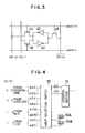
- the present embodiment additionally includes, in the same semiconductor memory circuit as the second embodiment, an input (output) selection switch 50 disposed on the input side of the address buffer 12, on the input side of the timing control circuit 30, on the input side of the input buffer 22A, and on the output side of the output buffer 22B, as illustrated in Fig. 4 as the input side of the address buffer 12 for example.
- an input (output) selection switch 50 disposed on the input side of the address buffer 12, on the input side of the timing control circuit 30, on the input side of the input buffer 22A, and on the output side of the output buffer 22B, as illustrated in Fig. 4 as the input side of the address buffer 12 for example.
- the input selection switch 50 disposed on the input side of the address buffer 12 for selecting the address lines is illustrated.
- the switch 50 assures the connection, to the address buffer 12, of any one of, besides the general lines A0S - A12S located in the typical PLD, long lines A0V - A12V, buses A0B - A12B, and input/output blocks (IOB) A0I - A12I. Selection of such connection lines is effected upon programming for the whole PLD by setting memory values Q0, Q1 in programming memories 50A, 50B upon the programming of the whole PLD.
- the input (excepting bit length select signals m0, m1) lines of the timing control circuit 30, the input lines of the address buffer 12, the input lines of the input buffer 22A, and the output lines of the output buffer 22B are made selectable, so that any association input/output signal can directly be inputted and outputted into and from the long line, bus, and IOB, etc., other than the general line in the typical PLD, and use of the general line to other applications is assured, further improving the multifunctional and general-purpose properties of the present memory circuit.
- the IOB is made selectable, direct inputs and outputs from and to the outside is assured.
- the input (output) selection switch was combined with the circuit of the second embodiment, the input (output) selection switch may be combined with the circuit of the first embodiment.
Landscapes
- Engineering & Computer Science (AREA)
- Theoretical Computer Science (AREA)
- Physics & Mathematics (AREA)
- General Engineering & Computer Science (AREA)
- General Physics & Mathematics (AREA)
- Static Random-Access Memory (AREA)
- Dram (AREA)
- Memory System (AREA)
Abstract
Description
- This invention relates to a semiconducter memory circuit, capable of changing the numbers of bits and words thereof, and more specifically to a multifunctional and general purpose semiconductor memory circuit which permits a user to electrically programming an arbitrary logic circuit at his hand and which is most preferable for use in a programmable logic device.
- There is conventionally known a programmable logic device (hereinafter simply referred to as a PLD), that is an integrated circuit with which a user can construct an arbitrary logic circuit at his hand.
- The PLD primarily includes a programmable logic element (hereinafter simply referred to as a PLE) which is configurable to establish a user's own logic, a circuit function-defining memory cell for defining the logic function of the PLE and a connection relationship among internal wirings, a programmable input/output block (hereinafter simply referred to as an IOB) for interfacing between external device packaging pins and an internal logic circuit (i.e., the PLE), and a programmable wiring for establishing a wiring path to connect input/output signals into/from the IOB and the PLE to a desired network.
- A semiconductor memory circuit for use in such a PLD is desirably variable in the numbers of bits and words meeting a user's wishes. However, such a prior memory circuit comprised of a gate array is impossible to change those numbers of bits and words after the wiring, even if they are variable upon wiring. To solve this, the memory circuit is obliged to have larger numbers of such bit and word, allowing unnecessary memory cells to be increased, followed by reduction of the degree of integration of the PLD and lowering of the utility of the memory circuit.
- In view of the drawbacks of the prior memory circuits, it is an object of the present invention to provide a multifunctional and highly flexible semiconductor memory circuit which is capable of utilizing to the utmost the infinite number of memory cells and which is switched to serve as an ordinary random access memory (hereinafter simply referred to as a RAM) as well as a first-in first-out memory (hereinafter simply referred to as a FIFO) on the basis of an external control signal.
- To achieve the above object, a semiconductor memory circuit according to the present invention is capable of changing the numbers of bits and words thereof, comprising: chip control means for at least selecting the number of bits of one word and switching between a random access memory function and a first-in first-out memory function; an address buffer having a function to alter an effective address length on the basis of a selected bit construction; an address counter for counting up a write address or a read address in each write or read operation when the first-in first-out memory function has been selected; a memory cell array; column and line decoders each for controlling said memory cell array on the basis of the selected bit construction; and an input/output buffer having a function to change an effective data length on the basis of the selected bit construction.
- In one aspect of the present invention, the write and read operations are independently executable when the first-in first-out memory function has been selected.
- In another aspect of the present invention, the memory circuit is programmable by itself as to whether or not it is used.
- In still another aspect of the present invention, the memory circuit further includes an input/output selection switch for enabling at least part of an input of the chip control means, an input of the address buffer, and inputs and outputs of the input/output buffer to be selected.
- In accordance with the present invention, the number of bits constituting one word is changeable on the basis of an external control signal, and the random access memory function and the first-in first-out memory function are switchable. A bit construction in the same integrated circuit can accordingly be changed by an external control signal, allowing the finite number of memory cells to be utilized to the utmost. The present memory circuit is switchable by an external control signal either to an ordinary random access memory or to a first-in first-out memory in which older data first disappears among stored data when it overflows, thereby improving multifunctional and general-purpose properties.
- In accordance with the present invention, write and read operations are respectively independently executable when the first-in first-out memory function has been selected. Hereby, sequential read and write operations are made possible, further improving multifunctional and general-purpose properties.
- Additionally, in accordance with the present invention, the present memory circuit is programmable by itself as to whether it is used or not. It is accordingly not needed, when the present memory circuit is not used, to instruct that fact through an external instruction input, allowing an instruction line for the just-mentioned external input to be available for another application, followed by further improvement of multifunctional and general-purpose properties.
- Furthermore, in accordance with the present invention, the input/output selection switch is provided for making selectable at least part of an input of the chip control means, an input of the address buffer, and inputs and outputs of the input/output buffer. Accordingly, at least part of the input of the chip control means, the input of the address buffer, and the inputs and outputs of the input/output buffer can directly be connected to another line in the PLD other than a general line in the same PLD which is ordinary used, such for example as a long line, a bus, and an input/output buffer, etc., allowing the general line to be employed for other applications, followed by further improvement of multifunctional and general-purpose properties. Particularly, when the input/output buffer is made selectable, direct input/output connection to the outside is possible.
- The exact nature of this invention, as well as other objects and advantages thereof, will be readily apparent from consideration of the following specification relating to the accompanying drawings, in which like reference characters designate the same or similar part throughout the figures thereof and wherein:
- Fig. 1 is a block diagram illustrating the arrangement of a first embodiment of a semiconductor memory circuit according to the present invention;
- Fig. 2 is a block diagram illustrating the arrangement of a second embodiment of the same;
- Fig. 3 is a circuit diagram illustrating the arrangement of a memory cell for use in the second embodiment; and
- Fig. 4 is a block diagram illustrating an input/output selection switch for use in a third embodiment.
- In the following, preferred embodiments of a semiconductor memory circuit according to the present invention will be described with reference to the accompanying drawings.
- In a first embodiment of the present invention, an 8 kbit semiconductor memory circuit will be taken as an illustrative example to which the present invention is applied.
- The circuit includes, as illustrated in Fig. 1, a
chip control circuit 10 for deciding whether the circuit is to be used or not, and selecting memory function (RAM mode or FIFO mode), and the number of bits of one word on the basis of external control signalsCS , FOM, m0 and m1, and further receiving an external write designation (request) signalWREQ and a read designation (request) signalRREQ , etc., anaddress buffer 12 having a function to select an effective address length among address inputs A0 - A12 set in conformity with the longest bit arrangement, on the basis of a bit construction assigned by thechip control circuit 10, anaddress counter 14 for counting up a write address or a read address at each write or read operation when the first-in first-out (FIFO) mode has been selected by thechip control circuit 10,memory cell arrays column decoders memory cell arrays 16A, 168 on the basis of the bit construction assigned by thechip control circuit 10, aline decoder 20 having same functions as thecolumn decoders buffer 22 for selecting an effective data length based on the bit construction assigned by thechip control circuit 10. - The
chip control circuit 10 includes an input terminal for receiving a chip select signalCS for selecting whether the present whole chip is to be used or not, an input terminal for receiving a mode control signal FOM which is to select whether the whole chip is operated with the ordinary (S) RAM mode or with the FIFO mode, input terminals for respectively receiving an external write request signalWREQ and a read request signalRREQ when the FIFO mode has been selected, and for respectively receiving a write enable signalWE for opening an input buffer and an output enable signalOE for opening an output buffer when the RAM mode has been selected, input terminals for respectively receiving bit length select signals m0, m1 for selecting the number of bits of one word, and an output teminal for issuing an alarm signal AWNG as it is found that a read address among addresses of theaddress counter 14 is coincident with an address +1 which has been written recently when the FIFO mode has been selected, i.e., when an address, which has not yet been written with any information, is assigned. Here, each overlined "-" signal means that the signal is true when it is at a "0" level (low level). - The
mode control signa 1 FOM can be set to select the ordinary RAM mode when it is "0" for example while selecting the FIFO mode when "1". - The bit length select signals m0, m1 can be set to select 1
word 1 bit when they are "0, 0", 1 word 4 bits when "1, 0", 1 word 8 bits when "0, 1", and 1word 16 bits when "1, 1", as listed in Table 1.Table 1 bit length select signal bit construction (bit/word) memory capcity (words) m1 m0 0 0 1 8192 0 1 4 2048 1 0 8 1024 1 1 16 512 - The
address buffer 12 selects an effective address length among address inputs A0 - A12 on the basis of the bit length control signal entered through thechip control circuit 10. In fact, all the address inputs A0 - A12 are valid when the bit length select signals m0, m1 are "0, 0˝, the address inputs A0 - A10 are valid when "1, 0", A0 - A9 are valid when "0, 1", and A0 - A8 are valid when "1, 1". - The
addess counter 14 counts up the write address and the read address at each write and read operation when the FIFO mode has been selected on the basis of the control signal entered through thechip control circuit 10. - The
chip control circuit 10 monitors counted values by theaddress counter 14, and issues the alarm signal AWNG when an address, which has not get been written with any information, is assigned for reading. Since in the present embodiment the alarm signal AWNG is issued on the basis of the counted value by theaddress counter 14 in the memory circuit, the arrangement of the memory circuit is very simplified compared with a prior case where such an alarm signal is issed on the basis of an external signal and the like. However, this function of issuing the alarm signal AWNG can be dispensed with. - It is noticed here that when the RAM mode is selected, any input signal simply passes through the
address counter 14. - The
column decoders line decoder 20 control address and data lines in thememory cell arrays chip control circuit 10. - The input/output (I/O)
buffer 22 selects an effective data length, on the basis of the bit construction assinged by thechip control circuit 10. - Now, it should be understand that although in the above embodiment the paired
memory cell arrays column decoders column decoders - In succession, a second embodiment of the semiconductor memory circuit according to the present invention will be described with reference to Fig. 2.
- The second embodiment includes additionally and independently, in the same semiconductor memory circuit as in the first embodiment, a
write address counter 14A and aread address counter 14B, awrite circuit 34A and awrite switch 36A both constituting the write column decoder, aread switch 36B and aread circuit 34B both constituting the read column decoder, aninput buffer 22A and anoutput buffer 22B, for the purpose of assuring indenpendent write and read operations when the FIFO mode has been selected. - Correspondingly, the chip control circuit includes a
timing control circuit 30 for receiving external control signals, a writeaddress switching circuit 32A, and a readaddress switching circuit 32B. - In addition, the write and read operations are executed respectively by independent signals WRES, WCLK and RRES, RCLK. Here, WRES and RRES are of write and read reset signals, respectively, and WCLK and RCLK are of write and read clock pulse signals, respectively.
- In the
timing control circuit 30, the chip select signal CS can be entered externally as in the first embodiment and further can also be set through aprogramming memory 30A. Hereby, the present memory circuit can be programmed as to whether it is used or not in itself, upon programming the whole PLD. Accordingly, if theprogramming memory 30 is programmed to be "1" in its status, then the external CS signal is valid, enabling the present memory circuit depending upon the status of the CS signal. In contrast, if theprogramming memory 30A is programmed to be "0", then the external CS signal is invalid, prohibiting the present memory circuit from being used at all times. The just-mentioned situation assures, when the present memory circuit is not used, the use of an instruction line for the external input to other applications because there is no need of successively instructing externally that the circuit is not to be used, thereby further improving multifunctional and general-purpose properties of the circuit. - In the
timing control circuit 30, the bit length select signals mo, m1 for selecting the number of bits of one word can also set inprogramming memories 30B, 30C upon the programming of the whole PLD. - The
memory cell array 16 is here integrally constructed differing from the case in the first embodiment. Each memory cell constituting thememory cell array 16 comprises a static RAM, which includes as illustrated in Fig. 3 for example, twoinformation holding inverters selection transistors bit - w) and read out (word - r, bit - r). - In the present embodiment, when the mode control signal FOM is "0" for example, the ordinary RAM mode is selected and the
address switching circuits address buffer 12. In contrast, when the mode cotrol signal FOM is "1" for examples the FIFO mode is selected and theaddress switching circuits address counters - Additionally, if the write and read addresses are coincident with each other, then writing has priority.
- Further, if the write address is filled up in writing, then the writing is interrupted, and if the write reset signal WRES is entered, then the writing is restarted from the oldest address for example.
- For other details, the description in the first embodiment is available and will be omitted here.
- In the present embodiment, the writing and the read out are independently executable in the FIFO mode, and hence successive operations are made possible, further improving multifunctional and general-purpose properties.
- In succession, a third embodiment of the present invention will be described with reference to Fig. 4.
- The present embodiment additionally includes, in the same semiconductor memory circuit as the second embodiment, an input (output)
selection switch 50 disposed on the input side of theaddress buffer 12, on the input side of thetiming control circuit 30, on the input side of theinput buffer 22A, and on the output side of theoutput buffer 22B, as illustrated in Fig. 4 as the input side of theaddress buffer 12 for example. - Referring to Fig. 4, the
input selection switch 50 disposed on the input side of theaddress buffer 12 for selecting the address lines is illustrated. Theswitch 50 assures the connection, to theaddress buffer 12, of any one of, besides the general lines A0S - A12S located in the typical PLD, long lines A0V - A12V, buses A0B - A12B, and input/output blocks (IOB) A0I - A12I. Selection of such connection lines is effected upon programming for the whole PLD by setting memory values Q0, Q1 inprogramming memories programming memories 50A - Although the same input (output) selection switches are additionally provided on the input side of the
timing control circuit 30, on the input side of theinput buffer 22A, and on the output side of theoutput buffer 22B, the detailed description will be omitted here. - In the present embodiment, the input (excepting bit length select signals m0, m1) lines of the
timing control circuit 30, the input lines of theaddress buffer 12, the input lines of theinput buffer 22A, and the output lines of theoutput buffer 22B are made selectable, so that any association input/output signal can directly be inputted and outputted into and from the long line, bus, and IOB, etc., other than the general line in the typical PLD, and use of the general line to other applications is assured, further improving the multifunctional and general-purpose properties of the present memory circuit. In particular, when the IOB is made selectable, direct inputs and outputs from and to the outside is assured. - It should now be understood that although in the present embodiment all of the input of the
address buffer 12, input of thetiming control circuit 30, input of theinput buffer 22A, and output of theoutput buffer 22B were made selectable, any part of those input and output may be fixed and the input (output) selection switch may be omitted. - Furthermore, although in the present embodiment, the input (output) selection switch was combined with the circuit of the second embodiment, the input (output) selection switch may be combined with the circuit of the first embodiment. Although certain preferred embodiments have been shown and described, it should be understood thus many changes and modifications may be made therein without departing from the scope of the appended claims.
Claims (9)
chip control means (10) for at least selecting the number of bits of one word and for switching between a random access memory function and a first-in first-out memory function;
an address buffer (12) having a function to alter an effective address length on the basis of a selected bit construction;
an address counter (14) for counting up a write address or a read address in each write or read operation when the first-in first-out memory function has been selected; a memory cell array (16A, 16B);
column and line decoders (18A, 18B; 20) each for controlling said memory cell array on the basis of the selected bit construction; and
an input/output buffer (22) having a function to change an effective data length on the basis of the selected bit construction.
timing control means (30) at least for selecting the number of bits of one word and for switching between a random access memory function and a first-in first-out memory function;
an address buffer (12) having a function to change an effective address length based upon a selected bit construction;
write and read address counters (14A, 14B) provided separately for counting up write and read addresses independently at each write and read operation when the first-in first-out memory function has been selected;
write address switching means (32A) for making valid an address input from said address buffer when the random access memory function has been selected, while making valid an address input from said write address counter when the first-in first-out memory function has been selectd;
read address switching means (32B) for making valid an address input from said address buffer when the random access memory function has been selected, while making valid an address input from said read address counter when the first-in first-out memory function has been selected;
input and output buffers (22A, 22B) provided separately having a function to change an effective data length based upon the selected bit construction;
a memory cell array (16);
write column and line decoders (34A, 36A, 20A) for controlling said memory cell array based upon the selected bit construction; and read column and line decoders (36B, 34B, 20B) for controlling said memory cell array based upon the selected bit construction.
Applications Claiming Priority (4)
| Application Number | Priority Date | Filing Date | Title |
|---|---|---|---|
| JP230745/88 | 1988-09-14 | ||
| JP23074588 | 1988-09-14 | ||
| JP39787/89 | 1989-02-20 | ||
| JP1039787A JPH02168496A (en) | 1988-09-14 | 1989-02-20 | Semiconductor memory circuit |
Publications (3)
| Publication Number | Publication Date |
|---|---|
| EP0359551A2 true EP0359551A2 (en) | 1990-03-21 |
| EP0359551A3 EP0359551A3 (en) | 1992-01-15 |
| EP0359551B1 EP0359551B1 (en) | 1994-12-28 |
Family
ID=26379174
Family Applications (1)
| Application Number | Title | Priority Date | Filing Date |
|---|---|---|---|
| EP89309306A Expired - Lifetime EP0359551B1 (en) | 1988-09-14 | 1989-09-13 | Semicoductor memory circuit |
Country Status (6)
| Country | Link |
|---|---|
| US (1) | US4985867A (en) |
| EP (1) | EP0359551B1 (en) |
| JP (1) | JPH02168496A (en) |
| KR (1) | KR940008133B1 (en) |
| CA (1) | CA1320576C (en) |
| DE (1) | DE68920243T2 (en) |
Cited By (20)
| Publication number | Priority date | Publication date | Assignee | Title |
|---|---|---|---|---|
| FR2702322A1 (en) * | 1993-03-01 | 1994-09-09 | Texas Instruments France | Memory at interconnection points, in particular for the communication of telecommunication terminals operating at different frequencies. |
| WO2010017015A1 (en) * | 2008-08-08 | 2010-02-11 | Rambus Inc. | Request-command encoding for reduced-data-rate testing |
| US8861247B2 (en) | 2009-04-27 | 2014-10-14 | Micron Technology, Inc. | Techniques for providing a direct injection semiconductor memory device |
| US8947965B2 (en) | 2009-07-27 | 2015-02-03 | Micron Technology Inc. | Techniques for providing a direct injection semiconductor memory device |
| US8964479B2 (en) | 2010-03-04 | 2015-02-24 | Micron Technology, Inc. | Techniques for sensing a semiconductor memory device |
| US8982633B2 (en) | 2009-05-22 | 2015-03-17 | Micron Technology, Inc. | Techniques for providing a direct injection semiconductor memory device |
| US9019759B2 (en) | 2010-03-15 | 2015-04-28 | Micron Technology, Inc. | Techniques for providing a semiconductor memory device |
| US9019788B2 (en) | 2008-01-24 | 2015-04-28 | Micron Technology, Inc. | Techniques for accessing memory cells |
| US9064730B2 (en) | 2009-03-04 | 2015-06-23 | Micron Technology, Inc. | Techniques for forming a contact to a buried diffusion layer in a semiconductor memory device |
| US9093311B2 (en) | 2009-03-31 | 2015-07-28 | Micron Technology, Inc. | Techniques for providing a semiconductor memory device |
| US9142264B2 (en) | 2010-05-06 | 2015-09-22 | Micron Technology, Inc. | Techniques for refreshing a semiconductor memory device |
| US9240496B2 (en) | 2009-04-30 | 2016-01-19 | Micron Technology, Inc. | Semiconductor device with floating gate and electrically floating body |
| US9257155B2 (en) | 2007-05-30 | 2016-02-09 | Micron Technology, Inc. | Integrated circuit having voltage generation circuitry for memory cell array, and method of operating and/or controlling same |
| US9263133B2 (en) | 2011-05-17 | 2016-02-16 | Micron Technology, Inc. | Techniques for providing a semiconductor memory device |
| US9276000B2 (en) | 2007-03-29 | 2016-03-01 | Micron Technology, Inc. | Manufacturing process for zero-capacitor random access memory circuits |
| US9331083B2 (en) | 2009-07-10 | 2016-05-03 | Micron Technology, Inc. | Techniques for providing a semiconductor memory device |
| US9553186B2 (en) | 2008-09-25 | 2017-01-24 | Micron Technology, Inc. | Recessed gate silicon-on-insulator floating body device with self-aligned lateral isolation |
| US9812179B2 (en) | 2009-11-24 | 2017-11-07 | Ovonyx Memory Technology, Llc | Techniques for reducing disturbance in a semiconductor memory device |
| US10304837B2 (en) | 2007-11-29 | 2019-05-28 | Ovonyx Memory Technology, Llc | Integrated circuit having memory cell array including barriers, and method of manufacturing same |
| US10418091B2 (en) | 2005-09-07 | 2019-09-17 | Ovonyx Memory Technology, Llc | Memory cell and memory cell array having an electrically floating body transistor, and methods of operating same |
Families Citing this family (63)
| Publication number | Priority date | Publication date | Assignee | Title |
|---|---|---|---|---|
| US5373959A (en) * | 1989-10-25 | 1994-12-20 | Hk-Plastics B.V. | Container with a cover |
| JPH0447587A (en) * | 1990-06-15 | 1992-02-17 | Oki Electric Ind Co Ltd | Semiconductor memory |
| JP2982920B2 (en) * | 1990-07-10 | 1999-11-29 | 三菱電機株式会社 | Semiconductor storage device |
| JP2743653B2 (en) * | 1991-09-20 | 1998-04-22 | 富士通株式会社 | Semiconductor storage device |
| JPH0676559A (en) * | 1992-06-26 | 1994-03-18 | Mitsubishi Electric Corp | First-in first-out memory device |
| US5365485A (en) * | 1993-11-22 | 1994-11-15 | Texas Instruments Incorporated | Fifo with fast retransmit mode |
| JPH07226079A (en) * | 1994-02-14 | 1995-08-22 | Matsushita Electric Ind Co Ltd | Semiconductor memory |
| KR0120592B1 (en) * | 1994-09-09 | 1997-10-20 | 김주용 | Address buffer having signal transform logic |
| JP2692638B2 (en) * | 1995-03-31 | 1997-12-17 | 日本電気株式会社 | Non-volatile semiconductor memory |
| JP2817679B2 (en) * | 1995-09-20 | 1998-10-30 | 日本電気株式会社 | Semiconductor memory |
| US5712820A (en) * | 1995-11-17 | 1998-01-27 | Cypress Semiconductor Corporation | Multiple word width memory array clocking scheme |
| US5809339A (en) * | 1995-12-06 | 1998-09-15 | Cypress Semiconductor Corp. | State machine design for generating half-full and half-empty flags in an asynchronous FIFO |
| US5712992A (en) * | 1995-12-06 | 1998-01-27 | Cypress Semiconductor Corporation | State machine design for generating empty and full flags in an asynchronous FIFO |
| US5963056A (en) * | 1995-12-14 | 1999-10-05 | Cypress Semiconductor Corp. | Full and empty flag generator for synchronous FIFOs |
| US5844423A (en) * | 1995-12-14 | 1998-12-01 | Cypress Semiconductor Corporation | Half-full flag generator for synchronous FIFOs |
| US5852748A (en) * | 1995-12-29 | 1998-12-22 | Cypress Semiconductor Corp. | Programmable read-write word line equality signal generation for FIFOs |
| US5682356A (en) * | 1996-01-11 | 1997-10-28 | Cypress Semiconductor Corp. | Multiple word width memory array clocking scheme for reading words from a memory array |
| US5661418A (en) * | 1996-03-13 | 1997-08-26 | Cypress Semiconductor Corp. | Signal generation decoder circuit and method |
| US6510486B1 (en) | 1996-03-25 | 2003-01-21 | Cypress Semiconductor Corp. | Clocking scheme for independently reading and writing multiple width words from a memory array |
| US5764967A (en) * | 1996-03-29 | 1998-06-09 | Cypress Semiconductor Corporation | Multiple frequency memory array clocking scheme for reading and writing multiple width digital words |
| US5715197A (en) | 1996-07-29 | 1998-02-03 | Xilinx, Inc. | Multiport RAM with programmable data port configuration |
| US5860160A (en) * | 1996-12-18 | 1999-01-12 | Cypress Semiconductor Corp. | High speed FIFO mark and retransmit scheme using latches and precharge |
| JPH1145562A (en) * | 1997-07-25 | 1999-02-16 | Mitsubishi Electric Corp | Semiconductor storage device |
| US6404660B1 (en) * | 1999-12-23 | 2002-06-11 | Rambus, Inc. | Semiconductor package with a controlled impedance bus and method of forming same |
| US7610447B2 (en) * | 2001-02-28 | 2009-10-27 | Rambus Inc. | Upgradable memory system with reconfigurable interconnect |
| US6889304B2 (en) | 2001-02-28 | 2005-05-03 | Rambus Inc. | Memory device supporting a dynamically configurable core organization |
| US7500075B1 (en) | 2001-04-17 | 2009-03-03 | Rambus Inc. | Mechanism for enabling full data bus utilization without increasing data granularity |
| TWI230392B (en) | 2001-06-18 | 2005-04-01 | Innovative Silicon Sa | Semiconductor device |
| US6825841B2 (en) * | 2001-09-07 | 2004-11-30 | Rambus Inc. | Granularity memory column access |
| US20040228168A1 (en) | 2003-05-13 | 2004-11-18 | Richard Ferrant | Semiconductor memory device and method of operating same |
| US7335934B2 (en) | 2003-07-22 | 2008-02-26 | Innovative Silicon S.A. | Integrated circuit device, and method of fabricating same |
| US8190808B2 (en) * | 2004-08-17 | 2012-05-29 | Rambus Inc. | Memory device having staggered memory operations |
| US7280428B2 (en) * | 2004-09-30 | 2007-10-09 | Rambus Inc. | Multi-column addressing mode memory system including an integrated circuit memory device |
| US7254075B2 (en) * | 2004-09-30 | 2007-08-07 | Rambus Inc. | Integrated circuit memory system having dynamic memory bank count and page size |
| US8595459B2 (en) | 2004-11-29 | 2013-11-26 | Rambus Inc. | Micro-threaded memory |
| US20060248305A1 (en) * | 2005-04-13 | 2006-11-02 | Wayne Fang | Memory device having width-dependent output latency |
| US7683430B2 (en) | 2005-12-19 | 2010-03-23 | Innovative Silicon Isi Sa | Electrically floating body memory cell and array, and method of operating or controlling same |
| US7492632B2 (en) | 2006-04-07 | 2009-02-17 | Innovative Silicon Isi Sa | Memory array having a programmable word length, and method of operating same |
| US7933142B2 (en) | 2006-05-02 | 2011-04-26 | Micron Technology, Inc. | Semiconductor memory cell and array using punch-through to program and read same |
| US20070260841A1 (en) | 2006-05-02 | 2007-11-08 | Hampel Craig E | Memory module with reduced access granularity |
| US8069377B2 (en) | 2006-06-26 | 2011-11-29 | Micron Technology, Inc. | Integrated circuit having memory array including ECC and column redundancy and method of operating the same |
| US7542340B2 (en) | 2006-07-11 | 2009-06-02 | Innovative Silicon Isi Sa | Integrated circuit including memory array having a segmented bit line architecture and method of controlling and/or operating same |
| KR101406604B1 (en) | 2007-01-26 | 2014-06-11 | 마이크론 테크놀로지, 인코포레이티드 | Floating-body dram transistor comprising source/drain regions separated from the gated body region |
| US8085594B2 (en) | 2007-06-01 | 2011-12-27 | Micron Technology, Inc. | Reading technique for memory cell with electrically floating body transistor |
| US8194487B2 (en) | 2007-09-17 | 2012-06-05 | Micron Technology, Inc. | Refreshing data of memory cells with electrically floating body transistors |
| US8349662B2 (en) | 2007-12-11 | 2013-01-08 | Micron Technology, Inc. | Integrated circuit having memory cell array, and method of manufacturing same |
| US8014195B2 (en) | 2008-02-06 | 2011-09-06 | Micron Technology, Inc. | Single transistor memory cell |
| US8189376B2 (en) | 2008-02-08 | 2012-05-29 | Micron Technology, Inc. | Integrated circuit having memory cells including gate material having high work function, and method of manufacturing same |
| US7957206B2 (en) | 2008-04-04 | 2011-06-07 | Micron Technology, Inc. | Read circuitry for an integrated circuit having memory cells and/or a memory cell array, and method of operating same |
| US7933140B2 (en) | 2008-10-02 | 2011-04-26 | Micron Technology, Inc. | Techniques for reducing a voltage swing |
| US7924630B2 (en) | 2008-10-15 | 2011-04-12 | Micron Technology, Inc. | Techniques for simultaneously driving a plurality of source lines |
| US8223574B2 (en) | 2008-11-05 | 2012-07-17 | Micron Technology, Inc. | Techniques for block refreshing a semiconductor memory device |
| US8213226B2 (en) | 2008-12-05 | 2012-07-03 | Micron Technology, Inc. | Vertical transistor memory cell and array |
| US8319294B2 (en) | 2009-02-18 | 2012-11-27 | Micron Technology, Inc. | Techniques for providing a source line plane |
| US8898439B2 (en) * | 2009-07-17 | 2014-11-25 | Macronix International Co., Ltd. | Serial flash memory and address transmission method thereof |
| US8677100B2 (en) * | 2009-07-17 | 2014-03-18 | Macronix International Co., Ltd. | Serial memory interface for extended address space |
| US8199595B2 (en) | 2009-09-04 | 2012-06-12 | Micron Technology, Inc. | Techniques for sensing a semiconductor memory device |
| US8310893B2 (en) | 2009-12-16 | 2012-11-13 | Micron Technology, Inc. | Techniques for reducing impact of array disturbs in a semiconductor memory device |
| US8416636B2 (en) | 2010-02-12 | 2013-04-09 | Micron Technology, Inc. | Techniques for controlling a semiconductor memory device |
| US8411513B2 (en) | 2010-03-04 | 2013-04-02 | Micron Technology, Inc. | Techniques for providing a semiconductor memory device having hierarchical bit lines |
| US8369177B2 (en) | 2010-03-05 | 2013-02-05 | Micron Technology, Inc. | Techniques for reading from and/or writing to a semiconductor memory device |
| US9559216B2 (en) | 2011-06-06 | 2017-01-31 | Micron Technology, Inc. | Semiconductor memory device and method for biasing same |
| US9268719B2 (en) | 2011-08-05 | 2016-02-23 | Rambus Inc. | Memory signal buffers and modules supporting variable access granularity |
Citations (5)
| Publication number | Priority date | Publication date | Assignee | Title |
|---|---|---|---|---|
| US4271480A (en) * | 1975-12-31 | 1981-06-02 | Compagnie Internationale Pour L'informatique Cii-Honeywell Bull | Apparatus enabling the transfer of data blocks of variable lengths between two memory interfaces of different widths |
| US4498155A (en) * | 1979-11-23 | 1985-02-05 | Texas Instruments Incorporated | Semiconductor integrated circuit memory device with both serial and random access arrays |
| US4706219A (en) * | 1985-04-10 | 1987-11-10 | Nec Corporation | Word length selectable memory |
| US4733376A (en) * | 1984-10-17 | 1988-03-22 | Fujitsu Limited | Semiconductor memory device having serial data input circuit and serial data output circuit |
| EP0272869A2 (en) * | 1986-12-19 | 1988-06-29 | Fujitsu Limited | Dual port type semiconductor memory device realizing a high speed read operation |
Family Cites Families (14)
| Publication number | Priority date | Publication date | Assignee | Title |
|---|---|---|---|---|
| JPS5255446A (en) * | 1975-10-31 | 1977-05-06 | Toshiba Corp | Information transfer control system |
| JPS58194193A (en) * | 1982-05-07 | 1983-11-12 | Toshiba Corp | Memory circuit |
| US4567579A (en) * | 1983-07-08 | 1986-01-28 | Texas Instruments Incorporated | Dynamic memory with high speed nibble mode |
| JPS60200287A (en) * | 1984-03-24 | 1985-10-09 | 株式会社東芝 | Memory unit |
| JPH0799616B2 (en) * | 1984-08-30 | 1995-10-25 | 三菱電機株式会社 | Semiconductor memory device |
| US4876671A (en) * | 1985-04-30 | 1989-10-24 | Texas Instruments Incorporated | Semiconductor dynamic memory device with metal-level selection of page mode or nibble mode |
| JPS61269288A (en) * | 1985-05-24 | 1986-11-28 | Nec Corp | Storage element module |
| US4685084A (en) * | 1985-06-07 | 1987-08-04 | Intel Corporation | Apparatus for selecting alternate addressing mode and read-only memory |
| JPS62139198A (en) * | 1985-12-11 | 1987-06-22 | Mitsubishi Electric Corp | Semiconductor memory device |
| US4694426A (en) * | 1985-12-20 | 1987-09-15 | Ncr Corporation | Asynchronous FIFO status circuit |
| JPS6364698A (en) * | 1986-09-04 | 1988-03-23 | Fujitsu Ltd | Memory device |
| JPH0711916B2 (en) * | 1986-09-19 | 1995-02-08 | 株式会社日立製作所 | Dual-port semiconductor memory |
| JPH07111834B2 (en) * | 1987-04-15 | 1995-11-29 | 株式会社日立製作所 | Serial access memory |
| JPH0697560B2 (en) * | 1987-11-19 | 1994-11-30 | 三菱電機株式会社 | Semiconductor memory device |
-
1989
- 1989-02-20 JP JP1039787A patent/JPH02168496A/en active Pending
- 1989-09-11 US US07/405,026 patent/US4985867A/en not_active Expired - Lifetime
- 1989-09-12 KR KR1019890013272A patent/KR940008133B1/en not_active IP Right Cessation
- 1989-09-13 DE DE68920243T patent/DE68920243T2/en not_active Expired - Fee Related
- 1989-09-13 EP EP89309306A patent/EP0359551B1/en not_active Expired - Lifetime
- 1989-09-13 CA CA000611252A patent/CA1320576C/en not_active Expired - Fee Related
Patent Citations (5)
| Publication number | Priority date | Publication date | Assignee | Title |
|---|---|---|---|---|
| US4271480A (en) * | 1975-12-31 | 1981-06-02 | Compagnie Internationale Pour L'informatique Cii-Honeywell Bull | Apparatus enabling the transfer of data blocks of variable lengths between two memory interfaces of different widths |
| US4498155A (en) * | 1979-11-23 | 1985-02-05 | Texas Instruments Incorporated | Semiconductor integrated circuit memory device with both serial and random access arrays |
| US4733376A (en) * | 1984-10-17 | 1988-03-22 | Fujitsu Limited | Semiconductor memory device having serial data input circuit and serial data output circuit |
| US4706219A (en) * | 1985-04-10 | 1987-11-10 | Nec Corporation | Word length selectable memory |
| EP0272869A2 (en) * | 1986-12-19 | 1988-06-29 | Fujitsu Limited | Dual port type semiconductor memory device realizing a high speed read operation |
Cited By (28)
| Publication number | Priority date | Publication date | Assignee | Title |
|---|---|---|---|---|
| EP0617530A1 (en) * | 1993-03-01 | 1994-09-28 | Texas Instruments France | Interconnection memory comprising an array of dual-port FIFO memories |
| FR2702322A1 (en) * | 1993-03-01 | 1994-09-09 | Texas Instruments France | Memory at interconnection points, in particular for the communication of telecommunication terminals operating at different frequencies. |
| US11031069B2 (en) | 2005-09-07 | 2021-06-08 | Ovonyx Memory Technology, Llc | Memory cell and memory cell array having an electrically floating body transistor, and methods of operating same |
| US10418091B2 (en) | 2005-09-07 | 2019-09-17 | Ovonyx Memory Technology, Llc | Memory cell and memory cell array having an electrically floating body transistor, and methods of operating same |
| US9276000B2 (en) | 2007-03-29 | 2016-03-01 | Micron Technology, Inc. | Manufacturing process for zero-capacitor random access memory circuits |
| US9257155B2 (en) | 2007-05-30 | 2016-02-09 | Micron Technology, Inc. | Integrated circuit having voltage generation circuitry for memory cell array, and method of operating and/or controlling same |
| US11081486B2 (en) | 2007-11-29 | 2021-08-03 | Ovonyx Memory Technology, Llc | Integrated circuit having memory cell array including barriers, and method of manufacturing same |
| US10304837B2 (en) | 2007-11-29 | 2019-05-28 | Ovonyx Memory Technology, Llc | Integrated circuit having memory cell array including barriers, and method of manufacturing same |
| US9019788B2 (en) | 2008-01-24 | 2015-04-28 | Micron Technology, Inc. | Techniques for accessing memory cells |
| US9111645B2 (en) | 2008-08-08 | 2015-08-18 | Rambus Inc. | Request-command encoding for reduced-data-rate testing |
| WO2010017015A1 (en) * | 2008-08-08 | 2010-02-11 | Rambus Inc. | Request-command encoding for reduced-data-rate testing |
| US9553186B2 (en) | 2008-09-25 | 2017-01-24 | Micron Technology, Inc. | Recessed gate silicon-on-insulator floating body device with self-aligned lateral isolation |
| US9064730B2 (en) | 2009-03-04 | 2015-06-23 | Micron Technology, Inc. | Techniques for forming a contact to a buried diffusion layer in a semiconductor memory device |
| US9093311B2 (en) | 2009-03-31 | 2015-07-28 | Micron Technology, Inc. | Techniques for providing a semiconductor memory device |
| US9425190B2 (en) | 2009-04-27 | 2016-08-23 | Micron Technology, Inc. | Techniques for providing a direct injection semiconductor memory device |
| US8861247B2 (en) | 2009-04-27 | 2014-10-14 | Micron Technology, Inc. | Techniques for providing a direct injection semiconductor memory device |
| US9240496B2 (en) | 2009-04-30 | 2016-01-19 | Micron Technology, Inc. | Semiconductor device with floating gate and electrically floating body |
| US8982633B2 (en) | 2009-05-22 | 2015-03-17 | Micron Technology, Inc. | Techniques for providing a direct injection semiconductor memory device |
| US9331083B2 (en) | 2009-07-10 | 2016-05-03 | Micron Technology, Inc. | Techniques for providing a semiconductor memory device |
| US9679612B2 (en) | 2009-07-27 | 2017-06-13 | Micron Technology, Inc. | Techniques for providing a direct injection semiconductor memory device |
| US8964461B2 (en) | 2009-07-27 | 2015-02-24 | Micron Technology, Inc. | Techniques for providing a direct injection semiconductor memory device |
| US8947965B2 (en) | 2009-07-27 | 2015-02-03 | Micron Technology Inc. | Techniques for providing a direct injection semiconductor memory device |
| US9812179B2 (en) | 2009-11-24 | 2017-11-07 | Ovonyx Memory Technology, Llc | Techniques for reducing disturbance in a semiconductor memory device |
| US8964479B2 (en) | 2010-03-04 | 2015-02-24 | Micron Technology, Inc. | Techniques for sensing a semiconductor memory device |
| US9524971B2 (en) | 2010-03-15 | 2016-12-20 | Micron Technology, Inc. | Techniques for providing a semiconductor memory device |
| US9019759B2 (en) | 2010-03-15 | 2015-04-28 | Micron Technology, Inc. | Techniques for providing a semiconductor memory device |
| US9142264B2 (en) | 2010-05-06 | 2015-09-22 | Micron Technology, Inc. | Techniques for refreshing a semiconductor memory device |
| US9263133B2 (en) | 2011-05-17 | 2016-02-16 | Micron Technology, Inc. | Techniques for providing a semiconductor memory device |
Also Published As
| Publication number | Publication date |
|---|---|
| EP0359551B1 (en) | 1994-12-28 |
| DE68920243T2 (en) | 1995-05-04 |
| JPH02168496A (en) | 1990-06-28 |
| DE68920243D1 (en) | 1995-02-09 |
| US4985867A (en) | 1991-01-15 |
| KR900005441A (en) | 1990-04-14 |
| CA1320576C (en) | 1993-07-20 |
| EP0359551A3 (en) | 1992-01-15 |
| KR940008133B1 (en) | 1994-09-03 |
Similar Documents
| Publication | Publication Date | Title |
|---|---|---|
| EP0359551A2 (en) | Semicoductor memory circuit | |
| US4684830A (en) | Output circuit for a programmable logic array | |
| US4933577A (en) | Output circuit for a programmable logic array | |
| US5701091A (en) | Routing resources for hierarchical FPGA | |
| US5003200A (en) | Programmable logic device having programmable wiring for connecting adjacent programmable logic elements through a single switch station | |
| US6986004B1 (en) | FIFO memory with programmable data port widths | |
| US5394034A (en) | Programmable logic array having programmable output driver drive capacity | |
| KR930018857A (en) | Programmable Logic Circuit | |
| US5248908A (en) | 3-state bidirectional buffer and portable semiconductor storage device incorporating the same | |
| US7480165B1 (en) | Microcontroller with programmable logic | |
| US5623221A (en) | Low noise MOSFET employing selective drive signals | |
| JPH04228174A (en) | Semiconductor memory | |
| US4706217A (en) | Sequential logic circuit | |
| JP2544020B2 (en) | Programmable logic element | |
| US5251174A (en) | Memory system | |
| US6400635B1 (en) | Memory circuitry for programmable logic integrated circuit devices | |
| US5632040A (en) | Microcomputer having reduced power consumption through impedance control and frequency reduction | |
| US5426432A (en) | IC card | |
| US4890262A (en) | Semiconductor memory with built-in defective bit relief circuit | |
| US5317536A (en) | Dual-port type semiconductor integrated memory circuit | |
| JPH0734184B2 (en) | Semiconductor device having chip select terminal pair | |
| US5402381A (en) | Semiconductor memory circuit having bit clear and/or register initialize function | |
| EP0617530A1 (en) | Interconnection memory comprising an array of dual-port FIFO memories | |
| KR940004363Y1 (en) | Input-output control circuit of plc | |
| JPH04247394A (en) | Memory cell |
Legal Events
| Date | Code | Title | Description |
|---|---|---|---|
| PUAI | Public reference made under article 153(3) epc to a published international application that has entered the european phase |
Free format text: ORIGINAL CODE: 0009012 |
|
| AK | Designated contracting states |
Kind code of ref document: A2 Designated state(s): DE FR GB NL |
|
| PUAL | Search report despatched |
Free format text: ORIGINAL CODE: 0009013 |
|
| AK | Designated contracting states |
Kind code of ref document: A3 Designated state(s): DE FR GB NL |
|
| RHK1 | Main classification (correction) |
Ipc: G11C 7/00 |
|
| 17P | Request for examination filed |
Effective date: 19920319 |
|
| 17Q | First examination report despatched |
Effective date: 19931001 |
|
| GRAA | (expected) grant |
Free format text: ORIGINAL CODE: 0009210 |
|
| AK | Designated contracting states |
Kind code of ref document: B1 Designated state(s): DE FR GB |
|
| REF | Corresponds to: |
Ref document number: 68920243 Country of ref document: DE Date of ref document: 19950209 |
|
| ET | Fr: translation filed | ||
| PLBE | No opposition filed within time limit |
Free format text: ORIGINAL CODE: 0009261 |
|
| STAA | Information on the status of an ep patent application or granted ep patent |
Free format text: STATUS: NO OPPOSITION FILED WITHIN TIME LIMIT |
|
| 26N | No opposition filed | ||
| REG | Reference to a national code |
Ref country code: GB Ref legal event code: IF02 |
|
| REG | Reference to a national code |
Ref country code: GB Ref legal event code: 732E |
|
| PGFP | Annual fee paid to national office [announced via postgrant information from national office to epo] |
Ref country code: GB Payment date: 20040908 Year of fee payment: 16 Ref country code: FR Payment date: 20040908 Year of fee payment: 16 |
|
| PGFP | Annual fee paid to national office [announced via postgrant information from national office to epo] |
Ref country code: DE Payment date: 20040909 Year of fee payment: 16 |
|
| PG25 | Lapsed in a contracting state [announced via postgrant information from national office to epo] |
Ref country code: GB Free format text: LAPSE BECAUSE OF NON-PAYMENT OF DUE FEES Effective date: 20050913 |
|
| PG25 | Lapsed in a contracting state [announced via postgrant information from national office to epo] |
Ref country code: DE Free format text: LAPSE BECAUSE OF NON-PAYMENT OF DUE FEES Effective date: 20060401 |
|
| GBPC | Gb: european patent ceased through non-payment of renewal fee |
Effective date: 20050913 |
|
| PG25 | Lapsed in a contracting state [announced via postgrant information from national office to epo] |
Ref country code: FR Free format text: LAPSE BECAUSE OF NON-PAYMENT OF DUE FEES Effective date: 20060531 |
|
| REG | Reference to a national code |
Ref country code: FR Ref legal event code: ST Effective date: 20060531 |