EP0363673A1 - Sputter-deposited nickel layer and process for depositing same - Google Patents
Sputter-deposited nickel layer and process for depositing same Download PDFInfo
- Publication number
- EP0363673A1 EP0363673A1 EP89117064A EP89117064A EP0363673A1 EP 0363673 A1 EP0363673 A1 EP 0363673A1 EP 89117064 A EP89117064 A EP 89117064A EP 89117064 A EP89117064 A EP 89117064A EP 0363673 A1 EP0363673 A1 EP 0363673A1
- Authority
- EP
- European Patent Office
- Prior art keywords
- substrate
- nickel layer
- layer
- nickel
- argon gas
- Prior art date
- Legal status (The legal status is an assumption and is not a legal conclusion. Google has not performed a legal analysis and makes no representation as to the accuracy of the status listed.)
- Granted
Links
- PXHVJJICTQNCMI-UHFFFAOYSA-N Nickel Chemical compound [Ni] PXHVJJICTQNCMI-UHFFFAOYSA-N 0.000 title claims abstract description 163
- 229910052759 nickel Inorganic materials 0.000 title claims abstract description 57
- 238000000034 method Methods 0.000 title claims abstract description 25
- 238000000151 deposition Methods 0.000 title claims abstract description 7
- XKRFYHLGVUSROY-UHFFFAOYSA-N Argon Chemical compound [Ar] XKRFYHLGVUSROY-UHFFFAOYSA-N 0.000 claims abstract description 90
- 239000007789 gas Substances 0.000 claims abstract description 60
- 239000000758 substrate Substances 0.000 claims abstract description 47
- 229910052786 argon Inorganic materials 0.000 claims abstract description 45
- 238000004544 sputter deposition Methods 0.000 claims abstract description 26
- 238000002441 X-ray diffraction Methods 0.000 claims abstract description 9
- 239000010936 titanium Substances 0.000 claims description 31
- 229910052719 titanium Inorganic materials 0.000 claims description 18
- 229910052710 silicon Inorganic materials 0.000 claims description 16
- RTAQQCXQSZGOHL-UHFFFAOYSA-N Titanium Chemical compound [Ti] RTAQQCXQSZGOHL-UHFFFAOYSA-N 0.000 claims description 10
- 239000010931 gold Substances 0.000 claims description 8
- XUIMIQQOPSSXEZ-UHFFFAOYSA-N Silicon Chemical compound [Si] XUIMIQQOPSSXEZ-UHFFFAOYSA-N 0.000 claims description 7
- 239000010703 silicon Substances 0.000 claims description 7
- PCHJSUWPFVWCPO-UHFFFAOYSA-N gold Chemical compound [Au] PCHJSUWPFVWCPO-UHFFFAOYSA-N 0.000 claims description 5
- 229910052737 gold Inorganic materials 0.000 claims description 5
- 238000001755 magnetron sputter deposition Methods 0.000 claims description 3
- XJKVPKYVPCWHFO-UHFFFAOYSA-N silicon;hydrate Chemical compound O.[Si] XJKVPKYVPCWHFO-UHFFFAOYSA-N 0.000 claims 1
- 238000005452 bending Methods 0.000 abstract description 3
- 150000002815 nickel Chemical class 0.000 abstract 1
- 235000012431 wafers Nutrition 0.000 description 27
- 230000035882 stress Effects 0.000 description 22
- 229910052751 metal Inorganic materials 0.000 description 13
- 239000002184 metal Substances 0.000 description 13
- 229910004339 Ti-Si Inorganic materials 0.000 description 7
- 229910010978 Ti—Si Inorganic materials 0.000 description 7
- 239000000853 adhesive Substances 0.000 description 4
- 230000001070 adhesive effect Effects 0.000 description 4
- 230000003247 decreasing effect Effects 0.000 description 3
- 239000006185 dispersion Substances 0.000 description 3
- 238000004519 manufacturing process Methods 0.000 description 3
- 229910052581 Si3N4 Inorganic materials 0.000 description 2
- 230000004888 barrier function Effects 0.000 description 2
- 238000010438 heat treatment Methods 0.000 description 2
- 239000002245 particle Substances 0.000 description 2
- 229920006395 saturated elastomer Polymers 0.000 description 2
- 239000004065 semiconductor Substances 0.000 description 2
- HQVNEWCFYHHQES-UHFFFAOYSA-N silicon nitride Chemical compound N12[Si]34N5[Si]62N3[Si]51N64 HQVNEWCFYHHQES-UHFFFAOYSA-N 0.000 description 2
- 229910052782 aluminium Inorganic materials 0.000 description 1
- XAGFODPZIPBFFR-UHFFFAOYSA-N aluminium Chemical compound [Al] XAGFODPZIPBFFR-UHFFFAOYSA-N 0.000 description 1
- 239000000356 contaminant Substances 0.000 description 1
- 239000013078 crystal Substances 0.000 description 1
- 230000008021 deposition Effects 0.000 description 1
- 239000000463 material Substances 0.000 description 1
- 238000005259 measurement Methods 0.000 description 1
- 230000008646 thermal stress Effects 0.000 description 1
- LEONUFNNVUYDNQ-UHFFFAOYSA-N vanadium atom Chemical compound [V] LEONUFNNVUYDNQ-UHFFFAOYSA-N 0.000 description 1
Images


Classifications
-
- C—CHEMISTRY; METALLURGY
- C23—COATING METALLIC MATERIAL; COATING MATERIAL WITH METALLIC MATERIAL; CHEMICAL SURFACE TREATMENT; DIFFUSION TREATMENT OF METALLIC MATERIAL; COATING BY VACUUM EVAPORATION, BY SPUTTERING, BY ION IMPLANTATION OR BY CHEMICAL VAPOUR DEPOSITION, IN GENERAL; INHIBITING CORROSION OF METALLIC MATERIAL OR INCRUSTATION IN GENERAL
- C23C—COATING METALLIC MATERIAL; COATING MATERIAL WITH METALLIC MATERIAL; SURFACE TREATMENT OF METALLIC MATERIAL BY DIFFUSION INTO THE SURFACE, BY CHEMICAL CONVERSION OR SUBSTITUTION; COATING BY VACUUM EVAPORATION, BY SPUTTERING, BY ION IMPLANTATION OR BY CHEMICAL VAPOUR DEPOSITION, IN GENERAL
- C23C14/00—Coating by vacuum evaporation, by sputtering or by ion implantation of the coating forming material
- C23C14/02—Pretreatment of the material to be coated
- C23C14/024—Deposition of sublayers, e.g. to promote adhesion of the coating
- C23C14/025—Metallic sublayers
-
- C—CHEMISTRY; METALLURGY
- C23—COATING METALLIC MATERIAL; COATING MATERIAL WITH METALLIC MATERIAL; CHEMICAL SURFACE TREATMENT; DIFFUSION TREATMENT OF METALLIC MATERIAL; COATING BY VACUUM EVAPORATION, BY SPUTTERING, BY ION IMPLANTATION OR BY CHEMICAL VAPOUR DEPOSITION, IN GENERAL; INHIBITING CORROSION OF METALLIC MATERIAL OR INCRUSTATION IN GENERAL
- C23C—COATING METALLIC MATERIAL; COATING MATERIAL WITH METALLIC MATERIAL; SURFACE TREATMENT OF METALLIC MATERIAL BY DIFFUSION INTO THE SURFACE, BY CHEMICAL CONVERSION OR SUBSTITUTION; COATING BY VACUUM EVAPORATION, BY SPUTTERING, BY ION IMPLANTATION OR BY CHEMICAL VAPOUR DEPOSITION, IN GENERAL
- C23C14/00—Coating by vacuum evaporation, by sputtering or by ion implantation of the coating forming material
- C23C14/06—Coating by vacuum evaporation, by sputtering or by ion implantation of the coating forming material characterised by the coating material
- C23C14/14—Metallic material, boron or silicon
- C23C14/16—Metallic material, boron or silicon on metallic substrates or on substrates of boron or silicon
- C23C14/165—Metallic material, boron or silicon on metallic substrates or on substrates of boron or silicon by cathodic sputtering
-
- C—CHEMISTRY; METALLURGY
- C23—COATING METALLIC MATERIAL; COATING MATERIAL WITH METALLIC MATERIAL; CHEMICAL SURFACE TREATMENT; DIFFUSION TREATMENT OF METALLIC MATERIAL; COATING BY VACUUM EVAPORATION, BY SPUTTERING, BY ION IMPLANTATION OR BY CHEMICAL VAPOUR DEPOSITION, IN GENERAL; INHIBITING CORROSION OF METALLIC MATERIAL OR INCRUSTATION IN GENERAL
- C23C—COATING METALLIC MATERIAL; COATING MATERIAL WITH METALLIC MATERIAL; SURFACE TREATMENT OF METALLIC MATERIAL BY DIFFUSION INTO THE SURFACE, BY CHEMICAL CONVERSION OR SUBSTITUTION; COATING BY VACUUM EVAPORATION, BY SPUTTERING, BY ION IMPLANTATION OR BY CHEMICAL VAPOUR DEPOSITION, IN GENERAL
- C23C14/00—Coating by vacuum evaporation, by sputtering or by ion implantation of the coating forming material
- C23C14/06—Coating by vacuum evaporation, by sputtering or by ion implantation of the coating forming material characterised by the coating material
- C23C14/14—Metallic material, boron or silicon
- C23C14/18—Metallic material, boron or silicon on other inorganic substrates
-
- H—ELECTRICITY
- H01—ELECTRIC ELEMENTS
- H01L—SEMICONDUCTOR DEVICES NOT COVERED BY CLASS H10
- H01L29/00—Semiconductor devices adapted for rectifying, amplifying, oscillating or switching, or capacitors or resistors with at least one potential-jump barrier or surface barrier, e.g. PN junction depletion layer or carrier concentration layer; Details of semiconductor bodies or of electrodes thereof ; Multistep manufacturing processes therefor
- H01L29/40—Electrodes ; Multistep manufacturing processes therefor
- H01L29/43—Electrodes ; Multistep manufacturing processes therefor characterised by the materials of which they are formed
- H01L29/45—Ohmic electrodes
- H01L29/456—Ohmic electrodes on silicon
-
- Y—GENERAL TAGGING OF NEW TECHNOLOGICAL DEVELOPMENTS; GENERAL TAGGING OF CROSS-SECTIONAL TECHNOLOGIES SPANNING OVER SEVERAL SECTIONS OF THE IPC; TECHNICAL SUBJECTS COVERED BY FORMER USPC CROSS-REFERENCE ART COLLECTIONS [XRACs] AND DIGESTS
- Y10—TECHNICAL SUBJECTS COVERED BY FORMER USPC
- Y10T—TECHNICAL SUBJECTS COVERED BY FORMER US CLASSIFICATION
- Y10T428/00—Stock material or miscellaneous articles
- Y10T428/12—All metal or with adjacent metals
- Y10T428/12493—Composite; i.e., plural, adjacent, spatially distinct metal components [e.g., layers, joint, etc.]
- Y10T428/12674—Ge- or Si-base component
-
- Y—GENERAL TAGGING OF NEW TECHNOLOGICAL DEVELOPMENTS; GENERAL TAGGING OF CROSS-SECTIONAL TECHNOLOGIES SPANNING OVER SEVERAL SECTIONS OF THE IPC; TECHNICAL SUBJECTS COVERED BY FORMER USPC CROSS-REFERENCE ART COLLECTIONS [XRACs] AND DIGESTS
- Y10—TECHNICAL SUBJECTS COVERED BY FORMER USPC
- Y10T—TECHNICAL SUBJECTS COVERED BY FORMER US CLASSIFICATION
- Y10T428/00—Stock material or miscellaneous articles
- Y10T428/12—All metal or with adjacent metals
- Y10T428/12493—Composite; i.e., plural, adjacent, spatially distinct metal components [e.g., layers, joint, etc.]
- Y10T428/12771—Transition metal-base component
- Y10T428/12861—Group VIII or IB metal-base component
- Y10T428/12889—Au-base component
-
- Y—GENERAL TAGGING OF NEW TECHNOLOGICAL DEVELOPMENTS; GENERAL TAGGING OF CROSS-SECTIONAL TECHNOLOGIES SPANNING OVER SEVERAL SECTIONS OF THE IPC; TECHNICAL SUBJECTS COVERED BY FORMER USPC CROSS-REFERENCE ART COLLECTIONS [XRACs] AND DIGESTS
- Y10—TECHNICAL SUBJECTS COVERED BY FORMER USPC
- Y10T—TECHNICAL SUBJECTS COVERED BY FORMER US CLASSIFICATION
- Y10T428/00—Stock material or miscellaneous articles
- Y10T428/12—All metal or with adjacent metals
- Y10T428/12493—Composite; i.e., plural, adjacent, spatially distinct metal components [e.g., layers, joint, etc.]
- Y10T428/12771—Transition metal-base component
- Y10T428/12861—Group VIII or IB metal-base component
- Y10T428/12944—Ni-base component
-
- Y—GENERAL TAGGING OF NEW TECHNOLOGICAL DEVELOPMENTS; GENERAL TAGGING OF CROSS-SECTIONAL TECHNOLOGIES SPANNING OVER SEVERAL SECTIONS OF THE IPC; TECHNICAL SUBJECTS COVERED BY FORMER USPC CROSS-REFERENCE ART COLLECTIONS [XRACs] AND DIGESTS
- Y10—TECHNICAL SUBJECTS COVERED BY FORMER USPC
- Y10T—TECHNICAL SUBJECTS COVERED BY FORMER US CLASSIFICATION
- Y10T428/00—Stock material or miscellaneous articles
- Y10T428/26—Web or sheet containing structurally defined element or component, the element or component having a specified physical dimension
Definitions
- the present invention relates to a nickel layer deposited by sputtering and having a reduced stress, and a process for depositing such a sputtered nickel layer.
- a consecutive sputtering of titanium, nickel and gold layers onto a semiconductor substrate or wafer to form a laminated metal electrode in which an argon pressure used during the sputtering is usually 2 to 10 mTorr, is known.
- This pressure range is adopted because, at a higher argon pressure, the electric resistivity of the deposited layer is high and the load on a vacuum pump becomes higher as the argon pressure is increased.
- the object of the present invention is to reduce the stress in the deposited nickel layer and to provide a process for forming such a layer by sputtering.
- a nickel layer formed on a substrate in which a percent ratio of an X-ray diffraction peak intensity of the (200) plane of the nickel layer to that of the (111) plane of the nickel layer is not less than 10%.
- a preferred embodiment of the present invention is a power element comprising a silicon substrate having a top surface and a rear surface, a doped region formed adjacent to the top surface of the substrate, a first electrode formed on the top surface of the substrate and electrically connected to the doped region, and a second electrode formed on the rear surface of the substrate, the second electrode including a nickel layer in which a percent ratio of an X-ray diffraction peak intensity of the (200) plane of the nickel layer to that of the (111) plane of the nickel layer is not less than 10 %.
- the second electrode of the power element preferably comprises a titanium layer deposited on the silicon substrate, a nickel layer deposited on the titanium layer, and a gold layer deposited on the nickel layer.
- the present invention was created by a finding of the inventors that the stress in the deposited nickel layer can be reduced by increasing the pressure of the argon gas during the sputtering.
- a process for sputtering nickel on a substrate comprising supplying an argon gas into a vacuum chamber, adjusting a pressure of the argon gas in the vacuum chamber to a predetermined value, ionizing the argon gas, bombarding a target containing nickel with the ionized argon gas to sputter nickel atoms, and depositing the sputtered nickel atoms onto the substrate, wherein said predetermined pressure of the argon gas is not lower than 12 mTorr, preferably not lower than 15 mTorr.
- the temperature of the substrate during the sputtering is 100 to 250°C.
- the pressure of the argon gas is preferably not higher than 25 mTorr.
- a sputtering device as shown in Fig. 1 was used for carrying out the following examples.
- the device was a DC parallel plane-type magnetron sputtering unit XM-8, manufactured by Varian. During the sputtering, the temperature of the substrate was kept at about 180°C and the pressure of the argon gas 21 supplied to the chamber 23 was adjusted to 20 mTorr.
- FIGS. 1A to 1F show the steps of forming a laminated metal electrode according to an Example of the present invention.
- 1 denotes a silicon (Si) substrate having a diameter of 3 inches and a thickness of 230 ⁇ m, in which a base region and an emitter region, etc. of a power bipolar transistor are formed (not shown) and on which an aluminum (Al) wiring layer 3 is then formed in a predetermined pattern, as shown in Fig. 1B, and a silicon nitride (Si3N4) layer 5 is then formed on the Al wiring layer 3, as shown in Fig. 1C.
- Si silicon
- Si3N4 silicon nitride
- a metal electrode for a collector electrode is then formed on the rear surface of the substrate 1 by the sputtering unit shown in Fig. 2.
- a carrying-in table 27 receives a wafer from a transport 25 and then descends to pass the wafer to a shuttle (not shown). The shuttle moves along the broken line in Fig. 2 and transfers the wafer first to a process table 29.
- a radio frequency power is connected to the process table 29 at a lower electric potential, and to a capture 31 at a higher electric potential, specifically ground level, and a sputtering is carried out at a power of 60 W for 180 seconds, whereby ionized argon (Ar+) bombards and etches the rear surface of the substrate 1 at a thickness of about 18 nm.
- the capture 31 is used to collect contaminants (native oxide, etc.) at the surface of the Si.
- 33 denotes a magnet for confining the discharge.
- the shuttle then transfers the wafer to a station 15 and places the wafer on a process table 35.
- a DC power is connected to the process table 35 at a higher electric potential, specifically ground level, and to a titanium (Ti)-containing target 37 at a lower electric potential, and a sputtering is carried out at a power of 2 kW for 75 seconds, whereby ionized argon (Ar+) bombards the target 37, and Ti atoms sputtered from the target 37 are deposited onto the Si substrate 1 to form a Ti layer 7 having a thickness of about 250 nm, as shown in Fig. 1D.
- the shuttle transfers the wafer to a station 17 and place the wafer on a process table 39.
- a DC power is connected to the process table 39 at a higher electric potential, specifically ground level, and to a nickel (Ni)-containing target 41 at a lower electric potential, and a sputtering is carried out at a power of 1 kW for 240 seconds, whereby ionized argon (Ar+) bombards the target 41, and Ni atoms sputtered from the target 41 are deposited onto the Ti layer 7 to form a Ni layer 9 having a thickness of about 600 nm, as shown in Fig.1E.
- the shuttle then transfers the wafer to a station 19 and places the wafer on a process table 43.
- a DC power is connected to the process table 43 at a higher electric potential, specifically ground level, and to a gold (Au)-containing target 45 at a lower electric potential, and a sputtering is carried out at a power of 0.5 kW for 12 seconds, whereby ionized argon (Ar+) bombards the target 45, and Au atoms sputtered from the target 45, are deposited onto the Ni layer 9 to form an Au layer 11 having a thickness of about 50 nm, as shown in Fig. 1F.
- the wafer with the thus formed metal laminate electrode is transferred to a taking-out lock table 47 which then ascends to pass the wafer to a transport 49.
- the Ar gas is introduced to a chamber 23 from a gas inlet 53 after passing through a mass flow meter 51.
- the pressure of the Ar gas is determined by the feed rate of the Ar gas adjusted by the mass flow meter 51 and the degree of evacuation of the chamber 23 by vacuum pumps.
- the vacuum pumps include a rotary pump 55, a turbo pump 57 and a cryo pump 59.
- the rotary pump 55 conducts a rough evacuation
- the turbo pump 57 conducts an intermediate evacuation and an evacuation of a lock chamber 61
- the cryo pump 59 conducts a determining evacuation.
- the deposited Ni layer 9 contains a very small amount of Ar gas in the layer 9, since the sputtering on the Ni layer is carried out in the Ar atmosphere.
- bipolar transistor The detailed structure of the bipolar transistor may be found, for example, in U.S. Serial No. 114,287 filed on October 29, 1987 (corresponding to Japanese Unexamined Patent Publication (Kokai) No. 63-114,259).
- the pressure of the argon gas was 20 mTorr.
- Figures 3 to 8 show results when the argon gas pressure was varied.
- Figure 3 shows the X-ray diffraction intensity of the Ni layer when the pressure of the argon gas was varied.
- the abscissa denotes the argon gas pressure and the ordinate denotes the ratio of the X-ray diffraction intensities of the peaks of the (200) plane to the (111) plane of the Ni layer in percent, i.e., I (200) /I (111) x 100.
- the measurement was carried out by an X-ray diffraction unit RAD II C, manufactured by Rigaku, under the conditions of 40 kV, 40 mA and room temperature.
- the rate of the (200) plane to the (111) plane is increased with the increase of the pressure of the argon gas.
- the reasons therefor are considered to be as follows.
- Nickel is a face-centered cubic lattice metal, and therefore, tends to deposit on the substrate in a manner such that the densest plane (111) of the crystal becomes parallel to the top surface of the substrate.
- the pressure of the argon gas is increased, however, the possibility of a collision of the Ni particles with the argon moleculars in the atmosphere is increased, which collision lowers the energy of the Ni particles so that a dispersion of the Ni grain size of the Ni layer and a dispersion of the orientation in the Ni layer occur.
- Figures 9A and 9B show models of such results.
- Figure 9A shows the case in which the Ar pressure is low, the (111) planes of Ni appear in parallel to the surface of Ti, and the polycrystalline Ni grain size is uniform.
- Figure 9B shows the case in which the Ar pressure is high, the (111) planes of Ni are decreased, and the polycrystalline Ni grain size becomes nonuniform.
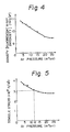
- Figure 4 shows the relationships between the argon gas pressure and the density of the deposited Ni layer.
- the abscissa denotes the argon gas pressure and the ordinate denotes the density of the Ni layer calculated from the fluorescence X-ray intensity.
- the Ar gas pressure With the increase of the Ar gas pressure, the polycrystalline Ni grain size becomes nonuniform, and therefore, the gaps between the Ni grains become large, so that the density of the Ni layer is lowered.
- Figure 8 shows the relationships between the Ar gas pressure and the full width of half maximum of the (111) plane of the Ni layer. This also indicates that, with an increase of the Ar gas pressure, the Ni grain size of the Ni layer becomes dispersed, and therefore, the full width of half maximum becomes larger.
- Figure 5 shows the tensile stress of the Ni layer in relation to the Ar gas pressure and indicates that the stress of the Ni layer is reduced by the increase of the Ar gas pressure.
- FIG 6 shows the Ti-Si peel-off area rate in relation to the Ar gas pressure.
- the Ti-Si peel-off area rate means that the rate of the area where the peel-off occurs between Ti and Si to the whole area of adhesion between Ti and Si, when the metal layer including the Ti layer and the other metal layers superimposed thereon was peeled from the Si.
- Figure 6 also indicates that the rate of the area where the peel-off occurs between Ti and Si is reduced when the Ar gas pressure is increased.
- Figure 7 shows the bend of the wafer in relation to the Ar gas pressure and indicates that the bend of the wafer is lessened with the increased of the Ar gas pressure. This is because, due to the increase of the Ar gas pressure, the density of the Ni layer is lowered, and therefore, the stress of the Ni layer is reduced.
- the bend of the wafer is sometimes over the limit for allowing the manufacture in an automatic line of a thickness of 350 ⁇ m, but by increasing the Ar pressure, the possibility of bend of the wafer over the limit is reduced.
- Figure 10 shows the relationships between the tensile stress of the Ni layer and the temperature of the substrate.
- the Ar gas pressure was 20 mTorr. It is seen from Fig. 9 that there is an optimum range of the substrate temperature for reducing the stress of the Ni layer, which optimum range is 100 to 250°C. At a temperature of the substrate below 100°C, the intrinsic stress of the Ni layer caused during the deposition becomes larger so that the tensile stress of the Ni layer is large as shown in Fig. 10. At a temperature of the substrate above 250°C, the thermal stress due to the difference of the thermal expansion coefficient between Si and Ni has an affect, so that the tensile stress of the Ni layer is again large as shown in Fig. 10.
- Figures 11 and 12 show the relationships of the tensile stress of the Ni layer with the Ti-Si peel-off rate and the bend of the wafer, respectively. It is seen from these figures that, when the tensile stress of the Ni layer is above 3 x 10⁸ N/m2, the Ti-Si peel-off rate is rapidly increased and the bend of the wafer is increased beyond the desired limit. Therefore, the tensile stress is preferably not more than 3 x 10⁸ N/m2. From Fig. 6, it is seen that the tensile stress of not more than 3 x 10⁸ N/m2 can be obtained by increasing the Ar gas pressure to 12 mTorr or more. Also, it is seen from Fig. 10 that the tensile stress of not more than 3 x 10⁸ N/m2 can be obtained by adjusting the substrate temperature to 100 - 250°C.
- Ti layer was used for an ohmic contact between the Ni layer and the Si substrate in the above Example, chlomium (Cr) or vanadium (V), etc. may be used instead of Ti, for the same purpose.
- the thickness of the Ti layer is not limited to 250 nm and may be 100 - 400 nm.
- the thickness of the Ni layer is not limited to 600 nm and may be 200 - 1000 nm.
- the (111) plane of the Ni layer is decreased and the density, and therefore, the stress of the Ni layer are reduced, whereby the bend of the wafer is reduced and an automatic transfer of the wafer becomes possible.
- a heat treatment at 450°C is carried out to improve the adhesive strength between Ti and Si and to prevent peel-off between the Ti and Si, which results in an enlarging of the bend of the wafer. Nevertheless, this heat treatment can be eliminated because the adhesive strength between the Ti and Si is improved by the reduction of stress of the Ni layer.
- the Ar gas pressure is not limited thereto and, by adopting an Ar gas pressure of not less than 12 mTorr as stated above, the tensile stress of the Ni layer can be made 3 x 10⁸ N/m2 or less and the Ti-Si peel-off rate and the bend of the wafer can be advantageously improved.
- the characteristics of the Ni layer are abruptly changed at around an Ar gas pressure of 15 mTorr and saturated around 20 mTorr.
- the peak intensity ratio is over 10% and almost saturated, and therefore, an Ni layer having stable characteristics can be obtained regardless of slight variations of the Ar gas pressure.
- the lower limit of the Ar gas pressure is described and the upper limit of the Ar gas pressure is not particularly limited and may be determined by the limit of the sputtering unit.
- the upper limit of the Ar gas pressure is determined by the electric resistivity of the metal.
- Figure 13 shows the electric resistivity of Ni and Ti layers in relation to the Ar gas pressure, in which ⁇ denotes the electric resistivity of the Ni layer and o denotes that of the Ti layer.
- the electric resistivity of the barrier metal is over 120 ⁇ cm, the ohmic contact between Si and Ti becomes nonuniform and the density of the Ti is decreased, whereby Si and Ni interdiffuse through the Ti layer and the adhesive strength is lowered. Therefore, the electric resistivity should be 120 ⁇ cm or less.
- the upper limit of the Ar gas pressure should be 25 mTorr.
- the present invention can provide a low stress metal layer on a substrate of various materials with a good adhesion. Particularly, it is useful for forming a rear electrode on a substrate of a power in which doped regions etc. are formed on the top surface thereof.
- a power element may be a DMOS and IGBT, etc.
- the unit for sputtering may be not only a parallel plane type but also a cylinder type, etc.
Abstract
Description
- The present invention relates to a nickel layer deposited by sputtering and having a reduced stress, and a process for depositing such a sputtered nickel layer.
- A consecutive sputtering of titanium, nickel and gold layers onto a semiconductor substrate or wafer to form a laminated metal electrode, in which an argon pressure used during the sputtering is usually 2 to 10 mTorr, is known. This pressure range is adopted because, at a higher argon pressure, the electric resistivity of the deposited layer is high and the load on a vacuum pump becomes higher as the argon pressure is increased.
- Nevertheless, in the conventional sputtering, a high stress occurs in particularly the deposited nickel layer, thereby bending the semiconductor wafer and reducing the adhesive strength of the deposited layers. Particularly, the bending of a wafer is a severe problem in an automatic manufacturing line, and wafers having a bend larger than 350 µm cannot be transferred in the automatic manufacturing line and thus must be manually transferred.
- The object of the present invention, therefore, is to reduce the stress in the deposited nickel layer and to provide a process for forming such a layer by sputtering.
- Thus, according to the present invention, there is provided a nickel layer formed on a substrate, in which a percent ratio of an X-ray diffraction peak intensity of the (200) plane of the nickel layer to that of the (111) plane of the nickel layer is not less than 10%.
- A preferred embodiment of the present invention is a power element comprising a silicon substrate having a top surface and a rear surface, a doped region formed adjacent to the top surface of the substrate, a first electrode formed on the top surface of the substrate and electrically connected to the doped region, and a second electrode formed on the rear surface of the substrate, the second electrode including a nickel layer in which a percent ratio of an X-ray diffraction peak intensity of the (200) plane of the nickel layer to that of the (111) plane of the nickel layer is not less than 10 %. The second electrode of the power element preferably comprises a titanium layer deposited on the silicon substrate, a nickel layer deposited on the titanium layer, and a gold layer deposited on the nickel layer.
- The present invention was created by a finding of the inventors that the stress in the deposited nickel layer can be reduced by increasing the pressure of the argon gas during the sputtering.
- Thus, according to the present invention, there is also provided a process for sputtering nickel on a substrate, comprising supplying an argon gas into a vacuum chamber, adjusting a pressure of the argon gas in the vacuum chamber to a predetermined value, ionizing the argon gas, bombarding a target containing nickel with the ionized argon gas to sputter nickel atoms, and depositing the sputtered nickel atoms onto the substrate, wherein said predetermined pressure of the argon gas is not lower than 12 mTorr, preferably not lower than 15 mTorr.
- Preferably, the temperature of the substrate during the sputtering is 100 to 250°C.
- During the depositing of a nickel layer onto a titanium layer formed on a substrate, the pressure of the argon gas is preferably not higher than 25 mTorr.
-
- Figures 1A to 1F are sectional views illustrating the steps of forming a laminated metal electrode according to the present invention;
- Fig. 2 is a sectional view of a sputtering device used for forming the laminated metal electrode;
- Fig. 3 shows the X-ray diffraction peak ratio I(200)/I(111) x 100 of a nickel layer in relation to the argon pressure;
- Fig. 4 shows the density of a nickel layer in relation to the argon pressure;
- Fig. 5 shows the layer stress of a nickel layer in relation to the argon pressure;
- Fig. 6 shows the rate of area of Ti-Si peel-off in relation to the argon pressure;
- Fig. 7 shows the bend of a wafer in relation to the argon pressure;
- Fig. 8 shows the full width of half maximum of the (111) plane of the Ni layer in relation to the argon pressure;
- Figs. 9A and 9B schematically illustrate the structures of deposited nickel layers on a substrate at low and high argon pressures;
- Fig. 10 shows the tensile strength of the nickel layer in relation to the temperature of the substrate;
- Fig. 11 shows the relationships between the rate of area of Ti-Si peel-off and the tensile strength of the nickel layer;
- Fig. 12 shows the relationships between the bend of the wafer and the tensile strength of the nickel layer; and
- Fig. 13 shows the electric resistivity in relation to the argon pressure.
- The present invention will be described with reference to the drawings.
- A sputtering device as shown in Fig. 1 was used for carrying out the following examples. The device was a DC parallel plane-type magnetron sputtering unit XM-8, manufactured by Varian. During the sputtering, the temperature of the substrate was kept at about 180°C and the pressure of the
argon gas 21 supplied to thechamber 23 was adjusted to 20 mTorr. - Figures 1A to 1F show the steps of forming a laminated metal electrode according to an Example of the present invention. In these figures, 1 denotes a silicon (Si) substrate having a diameter of 3 inches and a thickness of 230 µm, in which a base region and an emitter region, etc. of a power bipolar transistor are formed (not shown) and on which an aluminum (Al)
wiring layer 3 is then formed in a predetermined pattern, as shown in Fig. 1B, and a silicon nitride (Si₃N₄)layer 5 is then formed on theAl wiring layer 3, as shown in Fig. 1C. - After the elements are formed on the top surface of the
substrate 1, a metal electrode for a collector electrode is then formed on the rear surface of thesubstrate 1 by the sputtering unit shown in Fig. 2. In Fig. 2, a carrying-in table 27 receives a wafer from atransport 25 and then descends to pass the wafer to a shuttle (not shown). The shuttle moves along the broken line in Fig. 2 and transfers the wafer first to a process table 29. In astation 13, a radio frequency power is connected to the process table 29 at a lower electric potential, and to acapture 31 at a higher electric potential, specifically ground level, and a sputtering is carried out at a power of 60 W for 180 seconds, whereby ionized argon (Ar⁺) bombards and etches the rear surface of thesubstrate 1 at a thickness of about 18 nm. Thecapture 31 is used to collect contaminants (native oxide, etc.) at the surface of the Si. In Fig. 2, 33 denotes a magnet for confining the discharge. - The shuttle then transfers the wafer to a
station 15 and places the wafer on a process table 35. In thestation 15, a DC power is connected to the process table 35 at a higher electric potential, specifically ground level, and to a titanium (Ti)-containingtarget 37 at a lower electric potential, and a sputtering is carried out at a power of 2 kW for 75 seconds, whereby ionized argon (Ar⁺) bombards thetarget 37, and Ti atoms sputtered from thetarget 37 are deposited onto theSi substrate 1 to form aTi layer 7 having a thickness of about 250 nm, as shown in Fig. 1D. - Then the shuttle transfers the wafer to a
station 17 and place the wafer on a process table 39. In thestation 17, a DC power is connected to the process table 39 at a higher electric potential, specifically ground level, and to a nickel (Ni)-containingtarget 41 at a lower electric potential, and a sputtering is carried out at a power of 1 kW for 240 seconds, whereby ionized argon (Ar⁺) bombards thetarget 41, and Ni atoms sputtered from thetarget 41 are deposited onto theTi layer 7 to form aNi layer 9 having a thickness of about 600 nm, as shown in Fig.1E. - The shuttle then transfers the wafer to a
station 19 and places the wafer on a process table 43. In thestation 19, a DC power is connected to the process table 43 at a higher electric potential, specifically ground level, and to a gold (Au)-containingtarget 45 at a lower electric potential, and a sputtering is carried out at a power of 0.5 kW for 12 seconds, whereby ionized argon (Ar⁺) bombards thetarget 45, and Au atoms sputtered from thetarget 45, are deposited onto theNi layer 9 to form anAu layer 11 having a thickness of about 50 nm, as shown in Fig. 1F. - The wafer with the thus formed metal laminate electrode is transferred to a taking-out lock table 47 which then ascends to pass the wafer to a
transport 49. - The Ar gas is introduced to a
chamber 23 from agas inlet 53 after passing through amass flow meter 51. The pressure of the Ar gas is determined by the feed rate of the Ar gas adjusted by themass flow meter 51 and the degree of evacuation of thechamber 23 by vacuum pumps. The vacuum pumps include arotary pump 55, aturbo pump 57 and acryo pump 59. Therotary pump 55 conducts a rough evacuation, theturbo pump 57 conducts an intermediate evacuation and an evacuation of alock chamber 61, and thecryo pump 59 conducts a determining evacuation. - In the above process, the deposited
Ni layer 9 contains a very small amount of Ar gas in thelayer 9, since the sputtering on the Ni layer is carried out in the Ar atmosphere. - The detailed structure of the bipolar transistor may be found, for example, in U.S. Serial No. 114,287 filed on October 29, 1987 (corresponding to Japanese Unexamined Patent Publication (Kokai) No. 63-114,259).
- In the above example, the pressure of the argon gas was 20 mTorr. Figures 3 to 8 show results when the argon gas pressure was varied. Figure 3 shows the X-ray diffraction intensity of the Ni layer when the pressure of the argon gas was varied. The abscissa denotes the argon gas pressure and the ordinate denotes the ratio of the X-ray diffraction intensities of the peaks of the (200) plane to the (111) plane of the Ni layer in percent, i.e., I (200)/I(111) x 100. The measurement was carried out by an X-ray diffraction unit RADIIC, manufactured by Rigaku, under the conditions of 40 kV, 40 mA and room temperature. It is seen from Fig. 3 that the rate of the (200) plane to the (111) plane is increased with the increase of the pressure of the argon gas. The reasons therefor are considered to be as follows. Nickel is a face-centered cubic lattice metal, and therefore, tends to deposit on the substrate in a manner such that the densest plane (111) of the crystal becomes parallel to the top surface of the substrate. When the pressure of the argon gas is increased, however, the possibility of a collision of the Ni particles with the argon moleculars in the atmosphere is increased, which collision lowers the energy of the Ni particles so that a dispersion of the Ni grain size of the Ni layer and a dispersion of the orientation in the Ni layer occur. Figures 9A and 9B show models of such results. Figure 9A shows the case in which the Ar pressure is low, the (111) planes of Ni appear in parallel to the surface of Ti, and the polycrystalline Ni grain size is uniform. Figure 9B shows the case in which the Ar pressure is high, the (111) planes of Ni are decreased, and the polycrystalline Ni grain size becomes nonuniform.
- The above is supported by the results shown in Fig. 4. Figure 4 shows the relationships between the argon gas pressure and the density of the deposited Ni layer. The abscissa denotes the argon gas pressure and the ordinate denotes the density of the Ni layer calculated from the fluorescence X-ray intensity. With the increase of the Ar gas pressure, the polycrystalline Ni grain size becomes nonuniform, and therefore, the gaps between the Ni grains become large, so that the density of the Ni layer is lowered. Figure 8 shows the relationships between the Ar gas pressure and the full width of half maximum of the (111) plane of the Ni layer. This also indicates that, with an increase of the Ar gas pressure, the Ni grain size of the Ni layer becomes dispersed, and therefore, the full width of half maximum becomes larger.
- Figure 5 shows the tensile stress of the Ni layer in relation to the Ar gas pressure and indicates that the stress of the Ni layer is reduced by the increase of the Ar gas pressure.
- Figure 6 shows the Ti-Si peel-off area rate in relation to the Ar gas pressure. The Ti-Si peel-off area rate means that the rate of the area where the peel-off occurs between Ti and Si to the whole area of adhesion between Ti and Si, when the metal layer including the Ti layer and the other metal layers superimposed thereon was peeled from the Si. Figure 6 also indicates that the rate of the area where the peel-off occurs between Ti and Si is reduced when the Ar gas pressure is increased.
- Figure 7 shows the bend of the wafer in relation to the Ar gas pressure and indicates that the bend of the wafer is lessened with the increased of the Ar gas pressure. This is because, due to the increase of the Ar gas pressure, the density of the Ni layer is lowered, and therefore, the stress of the Ni layer is reduced. At a conventional Ar gas pressure of around 5 mTorr, the bend of the wafer is sometimes over the limit for allowing the manufacture in an automatic line of a thickness of 350 µm, but by increasing the Ar pressure, the possibility of bend of the wafer over the limit is reduced.
- Figure 10 shows the relationships between the tensile stress of the Ni layer and the temperature of the substrate. The Ar gas pressure was 20 mTorr. It is seen from Fig. 9 that there is an optimum range of the substrate temperature for reducing the stress of the Ni layer, which optimum range is 100 to 250°C. At a temperature of the substrate below 100°C, the intrinsic stress of the Ni layer caused during the deposition becomes larger so that the tensile stress of the Ni layer is large as shown in Fig. 10. At a temperature of the substrate above 250°C, the thermal stress due to the difference of the thermal expansion coefficient between Si and Ni has an affect, so that the tensile stress of the Ni layer is again large as shown in Fig. 10.
- Figures 11 and 12 show the relationships of the tensile stress of the Ni layer with the Ti-Si peel-off rate and the bend of the wafer, respectively. It is seen from these figures that, when the tensile stress of the Ni layer is above 3 x 10⁸ N/m², the Ti-Si peel-off rate is rapidly increased and the bend of the wafer is increased beyond the desired limit. Therefore, the tensile stress is preferably not more than 3 x 10⁸ N/m². From Fig. 6, it is seen that the tensile stress of not more than 3 x 10⁸ N/m² can be obtained by increasing the Ar gas pressure to 12 mTorr or more. Also, it is seen from Fig. 10 that the tensile stress of not more than 3 x 10⁸ N/m² can be obtained by adjusting the substrate temperature to 100 - 250°C.
- Although a Ti layer was used for an ohmic contact between the Ni layer and the Si substrate in the above Example, chlomium (Cr) or vanadium (V), etc. may be used instead of Ti, for the same purpose. The thickness of the Ti layer is not limited to 250 nm and may be 100 - 400 nm. The thickness of the Ni layer is not limited to 600 nm and may be 200 - 1000 nm.
- As described above, according to the present invention, by increasing the Ar gas pressure during sputtering, the (111) plane of the Ni layer is decreased and the density, and therefore, the stress of the Ni layer are reduced, whereby the bend of the wafer is reduced and an automatic transfer of the wafer becomes possible. Further, in a conventional process, a heat treatment at 450°C is carried out to improve the adhesive strength between Ti and Si and to prevent peel-off between the Ti and Si, which results in an enlarging of the bend of the wafer. Nevertheless, this heat treatment can be eliminated because the adhesive strength between the Ti and Si is improved by the reduction of stress of the Ni layer.
- Although an Ar gas pressure of 20 mTorr was adopted in the above Example, the Ar gas pressure is not limited thereto and, by adopting an Ar gas pressure of not less than 12 mTorr as stated above, the tensile stress of the Ni layer can be made 3 x 10⁸ N/m² or less and the Ti-Si peel-off rate and the bend of the wafer can be advantageously improved. As seen in Fig. 3 and 6, the characteristics of the Ni layer are abruptly changed at around an Ar gas pressure of 15 mTorr and saturated around 20 mTorr. Particularly, in Fig. 3 at an Ar gas pressure of 15 mTorr or more, the peak intensity ratio is over 10% and almost saturated, and therefore, an Ni layer having stable characteristics can be obtained regardless of slight variations of the Ar gas pressure.
- In the above, the lower limit of the Ar gas pressure is described and the upper limit of the Ar gas pressure is not particularly limited and may be determined by the limit of the sputtering unit.
- Where a Ti layer, etc., as a barrier metal, is inserted between a Si substrate and an Ni layer, the upper limit of the Ar gas pressure is determined by the electric resistivity of the metal. Figure 13 shows the electric resistivity of Ni and Ti layers in relation to the Ar gas pressure, in which Δ denotes the electric resistivity of the Ni layer and o denotes that of the Ti layer. Here, if the electric resistivity of the barrier metal is over 120 µΩ·cm, the ohmic contact between Si and Ti becomes nonuniform and the density of the Ti is decreased, whereby Si and Ni interdiffuse through the Ti layer and the adhesive strength is lowered. Therefore, the electric resistivity should be 120 µΩ·cm or less. Considering the dispersion of the electric resistivity of ±15 mΩ·cm when the Ar gas pressure is 25 mTorr, the upper limit of the Ar gas pressure should be 25 mTorr.
- The present invention can provide a low stress metal layer on a substrate of various materials with a good adhesion. Particularly, it is useful for forming a rear electrode on a substrate of a power in which doped regions etc. are formed on the top surface thereof. Such a power element may be a DMOS and IGBT, etc.
- The unit for sputtering may be not only a parallel plane type but also a cylinder type, etc.
Claims (16)
a silicon substrate having a top surface and a rear surface;
a doped region formed adjacent to the top surface of the substrate;
a first electrode formed on the top surface of the substrate and electrically connected to the doped region; and
a second electrode formed on the rear surface of the substrate, the second electrode including a nickel layer in which a percent ratio of an X-ray diffraction peak intensity of the (200) plane of the nickel layer to that of the (111) plane of the nickel layer is not less than 10%.
supplying an argon gas into a vacuum chamber,
adjusting a pressure of the argon gas in the vacuum chamber to a predetermined value,
ionizing the argon gas,
bombarding a target containing nickel with the ionized argon gas to sputter nickel atoms, and
depositing the sputtered nickel atoms onto the substrate, wherein said predetermined pressure of the argon gas is not lower than 12 mTorr.
Applications Claiming Priority (4)
| Application Number | Priority Date | Filing Date | Title |
|---|---|---|---|
| JP23165388 | 1988-09-15 | ||
| JP231653/88 | 1988-09-15 | ||
| JP1183502A JPH0784647B2 (en) | 1988-09-15 | 1989-07-14 | Nickel film and sputtering method for forming the same |
| JP183502/89 | 1989-07-14 |
Publications (2)
| Publication Number | Publication Date |
|---|---|
| EP0363673A1 true EP0363673A1 (en) | 1990-04-18 |
| EP0363673B1 EP0363673B1 (en) | 1993-08-18 |
Family
ID=26501916
Family Applications (1)
| Application Number | Title | Priority Date | Filing Date |
|---|---|---|---|
| EP89117064A Expired - Lifetime EP0363673B1 (en) | 1988-09-15 | 1989-09-14 | Sputter-deposited nickel layer and process for depositing same |
Country Status (4)
| Country | Link |
|---|---|
| US (1) | US5876861A (en) |
| EP (1) | EP0363673B1 (en) |
| JP (1) | JPH0784647B2 (en) |
| DE (1) | DE68908520T2 (en) |
Cited By (6)
| Publication number | Priority date | Publication date | Assignee | Title |
|---|---|---|---|---|
| EP0463362A2 (en) * | 1990-06-28 | 1992-01-02 | Nippondenso Co., Ltd. | Semiconductor device having metallic layers |
| US5527443A (en) * | 1992-05-28 | 1996-06-18 | Avx Corporation | Work holder for multiple electrical components |
| US5565838A (en) * | 1992-05-28 | 1996-10-15 | Avx Corporation | Varistors with sputtered terminations |
| WO2005021826A2 (en) * | 2003-08-29 | 2005-03-10 | Northrop Grumman Corporation | Titanium foil metallization product and process |
| US6997985B1 (en) | 1993-02-15 | 2006-02-14 | Semiconductor Energy Laboratory Co., Ltd. | Semiconductor, semiconductor device, and method for fabricating the same |
| US20210193470A1 (en) * | 2018-09-07 | 2021-06-24 | Sumitomo Heavy Industries, Ltd. | Semiconductor manufacturing method and semiconductor manufacturing device |
Families Citing this family (11)
| Publication number | Priority date | Publication date | Assignee | Title |
|---|---|---|---|---|
| EP0523701B1 (en) * | 1991-07-17 | 1998-01-07 | Denso Corporation | Method of forming electrodes of semiconductor device |
| CA2236049C (en) * | 1998-04-27 | 2006-07-25 | Computer Controlled Syringe Inc. | Syringe with detachable syringe barrel |
| US6342114B1 (en) * | 1999-03-31 | 2002-01-29 | Praxair S.T. Technology, Inc. | Nickel/vanadium sputtering target with ultra-low alpha emission |
| JP2003059757A (en) * | 2001-08-20 | 2003-02-28 | Toyo Metallizing Co Ltd | Metallic film transfer film for electronic component |
| JP3767585B2 (en) * | 2003-07-11 | 2006-04-19 | 株式会社デンソー | Semiconductor device |
| KR100558006B1 (en) * | 2003-11-17 | 2006-03-06 | 삼성전자주식회사 | Nickel salicide processes and methods of fabricating semiconductor devices using the same |
| FR2924232B1 (en) * | 2007-11-22 | 2009-11-27 | Saint Gobain | SUBSTRATE PROVIDED WITH A STACK WITH THERMAL PROPERTIES |
| US9017493B2 (en) | 2009-08-12 | 2015-04-28 | Ulvac, Inc. | Method of manufacturing a sputtering target and sputtering target |
| US20110048954A1 (en) * | 2009-09-03 | 2011-03-03 | U.S. Government As Represented By The Secretary Of The Army | Enhanced solderability using a substantially pure nickel layer deposited by physical vapor deposition |
| JP5620096B2 (en) * | 2009-12-29 | 2014-11-05 | ルネサスエレクトロニクス株式会社 | Manufacturing method of semiconductor device |
| TWI673177B (en) * | 2014-12-22 | 2019-10-01 | 日商信越化學工業股份有限公司 | Composite substrate, nano carbon film manufacturing method and nano carbon film |
Citations (2)
| Publication number | Priority date | Publication date | Assignee | Title |
|---|---|---|---|---|
| US3982908A (en) * | 1975-11-20 | 1976-09-28 | Rca Corporation | Nickel-gold-cobalt contact for silicon devices |
| EP0330122A1 (en) * | 1988-02-24 | 1989-08-30 | Siemens Aktiengesellschaft | Method of manufacturing a field-effect-controllable bipolar transistor |
Family Cites Families (13)
| Publication number | Priority date | Publication date | Assignee | Title |
|---|---|---|---|---|
| US3461054A (en) * | 1966-03-24 | 1969-08-12 | Bell Telephone Labor Inc | Cathodic sputtering from a cathodically biased target electrode having an rf potential superimposed on the cathodic bias |
| US3516915A (en) * | 1968-05-01 | 1970-06-23 | Bell Telephone Labor Inc | Sputtering technique |
| US3945903A (en) * | 1974-08-28 | 1976-03-23 | Shatterproof Glass Corporation | Sputter-coating of glass sheets or other substrates |
| JPS56142633A (en) * | 1980-04-08 | 1981-11-07 | Mitsubishi Electric Corp | Forming method for back electrode of semiconductor wafer |
| JPS5916322A (en) * | 1983-06-27 | 1984-01-27 | Toshiba Corp | Manufacture of magnetic film |
| US4513905A (en) * | 1983-07-29 | 1985-04-30 | The Perkin-Elmer Corporation | Integrated circuit metallization technique |
| JPS60134067A (en) * | 1983-12-19 | 1985-07-17 | 豊田合成株式会社 | Fiber article |
| US4588343A (en) * | 1984-05-18 | 1986-05-13 | Varian Associates, Inc. | Workpiece lifting and holding apparatus |
| US4610932A (en) * | 1984-12-06 | 1986-09-09 | At&T Technologies, Inc. | Electrical contacts |
| DE3788500T2 (en) * | 1986-10-31 | 1994-04-28 | Nippon Denso Co | Bipolar semiconductor transistor. |
| JPS63290268A (en) * | 1987-05-20 | 1988-11-28 | Fujitsu Ltd | Method for growing thin film |
| JPH07101736B2 (en) * | 1990-06-28 | 1995-11-01 | 日本電装株式会社 | Semiconductor device and manufacturing method thereof |
| US5361971A (en) * | 1993-01-19 | 1994-11-08 | Hughes Aircraft Company | Intermediate-temperature diffusion welding |
-
1989
- 1989-07-14 JP JP1183502A patent/JPH0784647B2/en not_active Expired - Lifetime
- 1989-09-14 EP EP89117064A patent/EP0363673B1/en not_active Expired - Lifetime
- 1989-09-14 DE DE89117064T patent/DE68908520T2/en not_active Expired - Lifetime
-
1996
- 1996-05-20 US US08/650,437 patent/US5876861A/en not_active Expired - Fee Related
Patent Citations (2)
| Publication number | Priority date | Publication date | Assignee | Title |
|---|---|---|---|---|
| US3982908A (en) * | 1975-11-20 | 1976-09-28 | Rca Corporation | Nickel-gold-cobalt contact for silicon devices |
| EP0330122A1 (en) * | 1988-02-24 | 1989-08-30 | Siemens Aktiengesellschaft | Method of manufacturing a field-effect-controllable bipolar transistor |
Non-Patent Citations (5)
| Title |
|---|
| JOURNAL OF VACUUM AND TECHNOLOGY, vol. 3, no. 3, part A, May/June 1985, American Vacuum Society, Woodbury, US; D.L. PACKWOOD et al.: "Contact metallization for producing stable bipolar microwave transistors" * |
| JOURNAL OF VACUUM SCIENCE & TECHNOLOGY, vol. 5, no. 3, part A, May/June 1987, pages 337-342, American Vacuum Society, Woodbury, US; Y.-K. CHAO et al.: "Porosity in Ni/Au metallization layers" * |
| JOURNAL OF VACUUM SCIENCE AND TECHNOLOGY, vol. 14, no. 1, January/February 1977, pages 164-168, The American Vacuum Society, Woodbury, US; J.A. THORNTON et al.: "Internal stresses in titanium, nickel, molybdenum, and tantalum film deposited by cylindical magnetron sputtering" * |
| THIN SOLID FILM, vol. 64, no. 1, November 1979, pages 121-128, Elsvier Sequoia S.A., Lausanne, CH; P.V. PLUNKETT et al.: "Stesses in sputter-deposited nickel and copper oxide" * |
| THIN SOLID FILMS, vol. 13, no. 2, 15th November 1972, pages 367-372, Elsevier Sequoia S.A., Lausanne, CH; B. NAVINSEK: "Stainless-steel, nickel and brass protective films produced by cathode sputtering" * |
Cited By (9)
| Publication number | Priority date | Publication date | Assignee | Title |
|---|---|---|---|---|
| EP0463362A2 (en) * | 1990-06-28 | 1992-01-02 | Nippondenso Co., Ltd. | Semiconductor device having metallic layers |
| EP0463362A3 (en) * | 1990-06-28 | 1992-11-19 | Nippondenso Co., Ltd. | Semiconductor device having metallic layers |
| US5614291A (en) * | 1990-06-28 | 1997-03-25 | Nippondenso Co., Ltd. | Semiconductor device and method of manufacturing the same |
| US5527443A (en) * | 1992-05-28 | 1996-06-18 | Avx Corporation | Work holder for multiple electrical components |
| US5565838A (en) * | 1992-05-28 | 1996-10-15 | Avx Corporation | Varistors with sputtered terminations |
| US6997985B1 (en) | 1993-02-15 | 2006-02-14 | Semiconductor Energy Laboratory Co., Ltd. | Semiconductor, semiconductor device, and method for fabricating the same |
| WO2005021826A2 (en) * | 2003-08-29 | 2005-03-10 | Northrop Grumman Corporation | Titanium foil metallization product and process |
| WO2005021826A3 (en) * | 2003-08-29 | 2005-12-01 | Northrop Grumman Corp | Titanium foil metallization product and process |
| US20210193470A1 (en) * | 2018-09-07 | 2021-06-24 | Sumitomo Heavy Industries, Ltd. | Semiconductor manufacturing method and semiconductor manufacturing device |
Also Published As
| Publication number | Publication date |
|---|---|
| DE68908520D1 (en) | 1993-09-23 |
| JPH0784647B2 (en) | 1995-09-13 |
| JPH02167890A (en) | 1990-06-28 |
| DE68908520T2 (en) | 1994-02-24 |
| EP0363673B1 (en) | 1993-08-18 |
| US5876861A (en) | 1999-03-02 |
Similar Documents
| Publication | Publication Date | Title |
|---|---|---|
| EP0363673B1 (en) | Sputter-deposited nickel layer and process for depositing same | |
| US5540820A (en) | Thin film forming method | |
| US6057237A (en) | Tantalum-containing barrier layers for copper | |
| US5439574A (en) | Method for successive formation of thin films | |
| EP0867525B1 (en) | Titanium nitride films | |
| US6521108B1 (en) | Diffusion bonded sputter target assembly and method of making same | |
| EP0407133A2 (en) | Semiconductor device and method of manufacturing such semiconductor device | |
| WO1998054377A2 (en) | Stress tuned tantalum and tantalum nitride films | |
| WO1999010921A1 (en) | Method of forming a barrier layer in a contact structure | |
| US6458255B2 (en) | Ultra-low resistivity tantalum films and methods for their deposition | |
| KR20010051101A (en) | Pvd-imp tungsten and tungsten nitride as a liner, barrier, and/or seed layer for tungsten, aluminum and copper applications | |
| US6315872B1 (en) | Coil for sputter deposition | |
| JP2951636B2 (en) | Method for manufacturing a metallization structure | |
| JP2714606B2 (en) | Wiring layer and its manufacturing method | |
| JP3033331B2 (en) | Manufacturing method of thin film wiring | |
| JP2718842B2 (en) | Method for manufacturing wiring metal film for semiconductor integrated circuit | |
| US4726983A (en) | Homogeneous fine grained metal film on substrate and manufacturing method thereof | |
| EP1147241B1 (en) | Diffusion bonded sputter target assembly and method of making same | |
| JP2894279B2 (en) | Metal thin film forming method | |
| US4923526A (en) | Homogeneous fine grained metal film on substrate and manufacturing method thereof | |
| US6255215B1 (en) | Semiconductor device having silicide layers formed using a collimated metal layer | |
| JP3523962B2 (en) | Sputtering apparatus and method for forming thin film by sputtering into hole | |
| JP3127494B2 (en) | Method for forming electrode of semiconductor device | |
| D’Couto et al. | In situ physical vapor deposition of ionized Ti and TiN thin films using hollow cathode magnetron plasma source | |
| JP3346794B2 (en) | Semiconductor device and method of forming the same |
Legal Events
| Date | Code | Title | Description |
|---|---|---|---|
| PUAI | Public reference made under article 153(3) epc to a published international application that has entered the european phase |
Free format text: ORIGINAL CODE: 0009012 |
|
| 17P | Request for examination filed |
Effective date: 19890914 |
|
| AK | Designated contracting states |
Kind code of ref document: A1 Designated state(s): DE FR GB |
|
| 17Q | First examination report despatched |
Effective date: 19920330 |
|
| GRAA | (expected) grant |
Free format text: ORIGINAL CODE: 0009210 |
|
| AK | Designated contracting states |
Kind code of ref document: B1 Designated state(s): DE FR GB |
|
| REF | Corresponds to: |
Ref document number: 68908520 Country of ref document: DE Date of ref document: 19930923 |
|
| ET | Fr: translation filed | ||
| PLBE | No opposition filed within time limit |
Free format text: ORIGINAL CODE: 0009261 |
|
| STAA | Information on the status of an ep patent application or granted ep patent |
Free format text: STATUS: NO OPPOSITION FILED WITHIN TIME LIMIT |
|
| REG | Reference to a national code |
Ref country code: GB Ref legal event code: 746 Effective date: 19940608 |
|
| 26N | No opposition filed | ||
| REG | Reference to a national code |
Ref country code: FR Ref legal event code: DL |
|
| REG | Reference to a national code |
Ref country code: GB Ref legal event code: IF02 |
|
| PGFP | Annual fee paid to national office [announced via postgrant information from national office to epo] |
Ref country code: FR Payment date: 20080915 Year of fee payment: 20 |
|
| PGFP | Annual fee paid to national office [announced via postgrant information from national office to epo] |
Ref country code: GB Payment date: 20080917 Year of fee payment: 20 |
|
| PGFP | Annual fee paid to national office [announced via postgrant information from national office to epo] |
Ref country code: DE Payment date: 20080926 Year of fee payment: 20 |
|
| REG | Reference to a national code |
Ref country code: GB Ref legal event code: PE20 Expiry date: 20090913 |
|
| PG25 | Lapsed in a contracting state [announced via postgrant information from national office to epo] |
Ref country code: GB Free format text: LAPSE BECAUSE OF EXPIRATION OF PROTECTION Effective date: 20090913 |