EP0365031A2 - Hologram stamper, method of manufacturing the same, and method of manufacturing hologram - Google Patents
Hologram stamper, method of manufacturing the same, and method of manufacturing hologram Download PDFInfo
- Publication number
- EP0365031A2 EP0365031A2 EP89119525A EP89119525A EP0365031A2 EP 0365031 A2 EP0365031 A2 EP 0365031A2 EP 89119525 A EP89119525 A EP 89119525A EP 89119525 A EP89119525 A EP 89119525A EP 0365031 A2 EP0365031 A2 EP 0365031A2
- Authority
- EP
- European Patent Office
- Prior art keywords
- hologram
- resin layer
- resin
- electron beam
- stamper
- Prior art date
- Legal status (The legal status is an assumption and is not a legal conclusion. Google has not performed a legal analysis and makes no representation as to the accuracy of the status listed.)
- Withdrawn
Links
- 238000004519 manufacturing process Methods 0.000 title claims description 40
- 229920005989 resin Polymers 0.000 claims abstract description 138
- 239000011347 resin Substances 0.000 claims abstract description 138
- 238000000034 method Methods 0.000 claims abstract description 38
- 229920005992 thermoplastic resin Polymers 0.000 claims abstract description 35
- 239000000758 substrate Substances 0.000 claims abstract description 28
- 238000010894 electron beam technology Methods 0.000 claims abstract description 25
- 239000004925 Acrylic resin Substances 0.000 claims abstract description 18
- 230000001678 irradiating effect Effects 0.000 claims abstract description 4
- 238000007731 hot pressing Methods 0.000 claims abstract description 3
- 229920002120 photoresistant polymer Polymers 0.000 claims description 40
- 239000000203 mixture Substances 0.000 claims description 19
- 229920006267 polyester film Polymers 0.000 claims description 19
- 239000011248 coating agent Substances 0.000 claims description 13
- 238000000576 coating method Methods 0.000 claims description 13
- 229920001187 thermosetting polymer Polymers 0.000 claims description 13
- 239000000178 monomer Substances 0.000 claims description 10
- 229910052751 metal Inorganic materials 0.000 claims description 7
- 239000002184 metal Substances 0.000 claims description 7
- 125000003118 aryl group Chemical group 0.000 claims description 5
- -1 ester acrylate Chemical class 0.000 claims description 5
- UHESRSKEBRADOO-UHFFFAOYSA-N ethyl carbamate;prop-2-enoic acid Chemical compound OC(=O)C=C.CCOC(N)=O UHESRSKEBRADOO-UHFFFAOYSA-N 0.000 claims description 5
- 125000001153 fluoro group Chemical group F* 0.000 claims description 5
- 125000003647 acryloyl group Chemical group O=C([*])C([H])=C([H])[H] 0.000 claims description 3
- KCTAWXVAICEBSD-UHFFFAOYSA-N prop-2-enoyloxy prop-2-eneperoxoate Chemical compound C=CC(=O)OOOC(=O)C=C KCTAWXVAICEBSD-UHFFFAOYSA-N 0.000 claims description 3
- 239000010410 layer Substances 0.000 abstract description 122
- 230000007261 regionalization Effects 0.000 abstract description 7
- 238000003825 pressing Methods 0.000 abstract description 2
- 239000002344 surface layer Substances 0.000 abstract description 2
- NIXOWILDQLNWCW-UHFFFAOYSA-M Acrylate Chemical compound [O-]C(=O)C=C NIXOWILDQLNWCW-UHFFFAOYSA-M 0.000 description 15
- XKRFYHLGVUSROY-UHFFFAOYSA-N Argon Chemical compound [Ar] XKRFYHLGVUSROY-UHFFFAOYSA-N 0.000 description 12
- KFZMGEQAYNKOFK-UHFFFAOYSA-N Isopropanol Chemical compound CC(C)O KFZMGEQAYNKOFK-UHFFFAOYSA-N 0.000 description 12
- 239000000243 solution Substances 0.000 description 12
- 239000011521 glass Substances 0.000 description 11
- QIVUCLWGARAQIO-OLIXTKCUSA-N (3s)-n-[(3s,5s,6r)-6-methyl-2-oxo-1-(2,2,2-trifluoroethyl)-5-(2,3,6-trifluorophenyl)piperidin-3-yl]-2-oxospiro[1h-pyrrolo[2,3-b]pyridine-3,6'-5,7-dihydrocyclopenta[b]pyridine]-3'-carboxamide Chemical compound C1([C@H]2[C@H](N(C(=O)[C@@H](NC(=O)C=3C=C4C[C@]5(CC4=NC=3)C3=CC=CN=C3NC5=O)C2)CC(F)(F)F)C)=C(F)C=CC(F)=C1F QIVUCLWGARAQIO-OLIXTKCUSA-N 0.000 description 6
- 229920000297 Rayon Polymers 0.000 description 6
- DAKWPKUUDNSNPN-UHFFFAOYSA-N Trimethylolpropane triacrylate Chemical compound C=CC(=O)OCC(CC)(COC(=O)C=C)COC(=O)C=C DAKWPKUUDNSNPN-UHFFFAOYSA-N 0.000 description 6
- 231100000987 absorbed dose Toxicity 0.000 description 6
- 239000003513 alkali Substances 0.000 description 6
- 229910052786 argon Inorganic materials 0.000 description 6
- 230000001588 bifunctional effect Effects 0.000 description 6
- 230000000052 comparative effect Effects 0.000 description 6
- 238000002156 mixing Methods 0.000 description 6
- DWKNOLCXIFYNFV-HSZRJFAPSA-N 2-[[(2r)-1-[1-[(4-chloro-3-methylphenyl)methyl]piperidin-4-yl]-5-oxopyrrolidine-2-carbonyl]amino]-n,n,6-trimethylpyridine-4-carboxamide Chemical compound CN(C)C(=O)C1=CC(C)=NC(NC(=O)[C@@H]2N(C(=O)CC2)C2CCN(CC=3C=C(C)C(Cl)=CC=3)CC2)=C1 DWKNOLCXIFYNFV-HSZRJFAPSA-N 0.000 description 5
- 238000001723 curing Methods 0.000 description 5
- 230000018109 developmental process Effects 0.000 description 5
- 150000002148 esters Chemical class 0.000 description 5
- 229920001721 polyimide Polymers 0.000 description 5
- 230000005855 radiation Effects 0.000 description 5
- KMIOJWCYOHBUJS-HAKPAVFJSA-N vorolanib Chemical compound C1N(C(=O)N(C)C)CC[C@@H]1NC(=O)C1=C(C)NC(\C=C/2C3=CC(F)=CC=C3NC\2=O)=C1C KMIOJWCYOHBUJS-HAKPAVFJSA-N 0.000 description 5
- 238000004049 embossing Methods 0.000 description 4
- 239000000463 material Substances 0.000 description 4
- AYOOGWWGECJQPI-NSHDSACASA-N n-[(1s)-1-(5-fluoropyrimidin-2-yl)ethyl]-3-(3-propan-2-yloxy-1h-pyrazol-5-yl)imidazo[4,5-b]pyridin-5-amine Chemical compound N1C(OC(C)C)=CC(N2C3=NC(N[C@@H](C)C=4N=CC(F)=CN=4)=CC=C3N=C2)=N1 AYOOGWWGECJQPI-NSHDSACASA-N 0.000 description 4
- 239000002904 solvent Substances 0.000 description 4
- 229920001169 thermoplastic Polymers 0.000 description 4
- 239000004416 thermosoftening plastic Substances 0.000 description 4
- DKEGCUDAFWNSSO-UHFFFAOYSA-N 1,8-dibromooctane Chemical compound BrCCCCCCCCBr DKEGCUDAFWNSSO-UHFFFAOYSA-N 0.000 description 3
- DBCAQXHNJOFNGC-UHFFFAOYSA-N 4-bromo-1,1,1-trifluorobutane Chemical class FC(F)(F)CCCBr DBCAQXHNJOFNGC-UHFFFAOYSA-N 0.000 description 3
- 239000004642 Polyimide Substances 0.000 description 3
- 229920001646 UPILEX Polymers 0.000 description 3
- TUOBEAZXHLTYLF-UHFFFAOYSA-N [2-(hydroxymethyl)-2-(prop-2-enoyloxymethyl)butyl] prop-2-enoate Chemical compound C=CC(=O)OCC(CO)(CC)COC(=O)C=C TUOBEAZXHLTYLF-UHFFFAOYSA-N 0.000 description 3
- FHLPGTXWCFQMIU-UHFFFAOYSA-N [4-[2-(4-prop-2-enoyloxyphenyl)propan-2-yl]phenyl] prop-2-enoate Chemical class C=1C=C(OC(=O)C=C)C=CC=1C(C)(C)C1=CC=C(OC(=O)C=C)C=C1 FHLPGTXWCFQMIU-UHFFFAOYSA-N 0.000 description 3
- 239000003795 chemical substances by application Substances 0.000 description 3
- SLCVBVWXLSEKPL-UHFFFAOYSA-N neopentyl glycol Chemical class OCC(C)(C)CO SLCVBVWXLSEKPL-UHFFFAOYSA-N 0.000 description 3
- 229920000728 polyester Polymers 0.000 description 3
- 238000010345 tape casting Methods 0.000 description 3
- 229940096522 trimethylolpropane triacrylate Drugs 0.000 description 3
- BIIBYWQGRFWQKM-JVVROLKMSA-N (2S)-N-[4-(cyclopropylamino)-3,4-dioxo-1-[(3S)-2-oxopyrrolidin-3-yl]butan-2-yl]-2-[[(E)-3-(2,4-dichlorophenyl)prop-2-enoyl]amino]-4,4-dimethylpentanamide Chemical compound CC(C)(C)C[C@@H](C(NC(C[C@H](CCN1)C1=O)C(C(NC1CC1)=O)=O)=O)NC(/C=C/C(C=CC(Cl)=C1)=C1Cl)=O BIIBYWQGRFWQKM-JVVROLKMSA-N 0.000 description 2
- QTKPMCIBUROOGY-UHFFFAOYSA-N 2,2,2-trifluoroethyl 2-methylprop-2-enoate Chemical compound CC(=C)C(=O)OCC(F)(F)F QTKPMCIBUROOGY-UHFFFAOYSA-N 0.000 description 2
- RUEKTOVLVIXOHT-UHFFFAOYSA-N 2,2,3,3,4,4,5,5,6,6,7,7,8,8,8-pentadecafluorooctyl 2-methylprop-2-enoate Chemical compound CC(=C)C(=O)OCC(F)(F)C(F)(F)C(F)(F)C(F)(F)C(F)(F)C(F)(F)C(F)(F)F RUEKTOVLVIXOHT-UHFFFAOYSA-N 0.000 description 2
- PUGOMSLRUSTQGV-UHFFFAOYSA-N 2,3-di(prop-2-enoyloxy)propyl prop-2-enoate Chemical class C=CC(=O)OCC(OC(=O)C=C)COC(=O)C=C PUGOMSLRUSTQGV-UHFFFAOYSA-N 0.000 description 2
- 229920000178 Acrylic resin Polymers 0.000 description 2
- HTMMMSIQFWMMIJ-UHFFFAOYSA-N [3-[2,2-dimethyl-3-(6-prop-2-enoyloxyhexanoyloxy)propanoyl]oxy-2,2-dimethylpropyl] 6-prop-2-enoyloxyhexanoate Chemical compound C=CC(=O)OCCCCCC(=O)OCC(C)(C)COC(=O)C(C)(C)COC(=O)CCCCCOC(=O)C=C HTMMMSIQFWMMIJ-UHFFFAOYSA-N 0.000 description 2
- YNTQTLGBCMXNFX-UHFFFAOYSA-N [5-ethyl-2-(2-methyl-1-prop-2-enoyloxypropan-2-yl)-1,3-dioxan-5-yl]methyl prop-2-enoate Chemical compound C=CC(=O)OCC1(CC)COC(C(C)(C)COC(=O)C=C)OC1 YNTQTLGBCMXNFX-UHFFFAOYSA-N 0.000 description 2
- 230000000903 blocking effect Effects 0.000 description 2
- 229920001577 copolymer Polymers 0.000 description 2
- YDKNBNOOCSNPNS-UHFFFAOYSA-N methyl 1,3-benzoxazole-2-carboxylate Chemical compound C1=CC=C2OC(C(=O)OC)=NC2=C1 YDKNBNOOCSNPNS-UHFFFAOYSA-N 0.000 description 2
- 229920000515 polycarbonate Polymers 0.000 description 2
- 239000004417 polycarbonate Substances 0.000 description 2
- 238000004528 spin coating Methods 0.000 description 2
- 238000001771 vacuum deposition Methods 0.000 description 2
- 229920002554 vinyl polymer Polymers 0.000 description 2
- 238000009736 wetting Methods 0.000 description 2
- JTCVKNUSIGHJRG-UHFFFAOYSA-N 1,1,1,2,3,3,3-heptafluoropropan-2-yl prop-2-enoate Chemical compound FC(F)(F)C(F)(C(F)(F)F)OC(=O)C=C JTCVKNUSIGHJRG-UHFFFAOYSA-N 0.000 description 1
- MNSWITGNWZSAMC-UHFFFAOYSA-N 1,1,1,3,3,3-hexafluoropropan-2-yl prop-2-enoate Chemical compound FC(F)(F)C(C(F)(F)F)OC(=O)C=C MNSWITGNWZSAMC-UHFFFAOYSA-N 0.000 description 1
- KOMNUTZXSVSERR-UHFFFAOYSA-N 1,3,5-tris(prop-2-enyl)-1,3,5-triazinane-2,4,6-trione Chemical compound C=CCN1C(=O)N(CC=C)C(=O)N(CC=C)C1=O KOMNUTZXSVSERR-UHFFFAOYSA-N 0.000 description 1
- VBHXIMACZBQHPX-UHFFFAOYSA-N 2,2,2-trifluoroethyl prop-2-enoate Chemical compound FC(F)(F)COC(=O)C=C VBHXIMACZBQHPX-UHFFFAOYSA-N 0.000 description 1
- PLXOUIVCSUBZIX-UHFFFAOYSA-N 2,2,3,3,4,4,4-heptafluorobutyl prop-2-enoate Chemical compound FC(F)(F)C(F)(F)C(F)(F)COC(=O)C=C PLXOUIVCSUBZIX-UHFFFAOYSA-N 0.000 description 1
- GIFZJPXYIFPWKS-UHFFFAOYSA-N 2,3-bis(difluoroamino)propyl prop-2-enoate Chemical compound FN(F)CC(N(F)F)COC(=O)C=C GIFZJPXYIFPWKS-UHFFFAOYSA-N 0.000 description 1
- RDFQSFOGKVZWKF-UHFFFAOYSA-N 3-hydroxy-2,2-dimethylpropanoic acid Chemical compound OCC(C)(C)C(O)=O RDFQSFOGKVZWKF-UHFFFAOYSA-N 0.000 description 1
- ZSSPEHLUBWYODL-UHFFFAOYSA-N 4,4,5,5-tetrafluoro-2-methylidene-5-(trifluoromethoxy)pentanoic acid Chemical compound OC(=O)C(=C)CC(F)(F)C(F)(F)OC(F)(F)F ZSSPEHLUBWYODL-UHFFFAOYSA-N 0.000 description 1
- DEWCEAYZKNTYPQ-UHFFFAOYSA-N 4,4-difluoro-2-methylidene-4-nitrobutanoic acid Chemical compound OC(=O)C(=C)CC(F)(F)[N+]([O-])=O DEWCEAYZKNTYPQ-UHFFFAOYSA-N 0.000 description 1
- UXHQLGLGLZKHTC-CUNXSJBXSA-N 4-[(3s,3ar)-3-cyclopentyl-7-(4-hydroxypiperidine-1-carbonyl)-3,3a,4,5-tetrahydropyrazolo[3,4-f]quinolin-2-yl]-2-chlorobenzonitrile Chemical compound C1CC(O)CCN1C(=O)C1=CC=C(C=2[C@@H]([C@H](C3CCCC3)N(N=2)C=2C=C(Cl)C(C#N)=CC=2)CC2)C2=N1 UXHQLGLGLZKHTC-CUNXSJBXSA-N 0.000 description 1
- HFGHRUCCKVYFKL-UHFFFAOYSA-N 4-ethoxy-2-piperazin-1-yl-7-pyridin-4-yl-5h-pyrimido[5,4-b]indole Chemical compound C1=C2NC=3C(OCC)=NC(N4CCNCC4)=NC=3C2=CC=C1C1=CC=NC=C1 HFGHRUCCKVYFKL-UHFFFAOYSA-N 0.000 description 1
- NLHHRLWOUZZQLW-UHFFFAOYSA-N Acrylonitrile Chemical compound C=CC#N NLHHRLWOUZZQLW-UHFFFAOYSA-N 0.000 description 1
- 229930185605 Bisphenol Natural products 0.000 description 1
- 229920000298 Cellophane Polymers 0.000 description 1
- RYGMFSIKBFXOCR-UHFFFAOYSA-N Copper Chemical compound [Cu] RYGMFSIKBFXOCR-UHFFFAOYSA-N 0.000 description 1
- OFOBLEOULBTSOW-UHFFFAOYSA-N Malonic acid Chemical compound OC(=O)CC(O)=O OFOBLEOULBTSOW-UHFFFAOYSA-N 0.000 description 1
- 239000004640 Melamine resin Substances 0.000 description 1
- 229920000877 Melamine resin Polymers 0.000 description 1
- 239000004697 Polyetherimide Substances 0.000 description 1
- 239000004734 Polyphenylene sulfide Substances 0.000 description 1
- 239000004743 Polypropylene Substances 0.000 description 1
- 239000004793 Polystyrene Substances 0.000 description 1
- 206010037660 Pyrexia Diseases 0.000 description 1
- BQCADISMDOOEFD-UHFFFAOYSA-N Silver Chemical compound [Ag] BQCADISMDOOEFD-UHFFFAOYSA-N 0.000 description 1
- ATJFFYVFTNAWJD-UHFFFAOYSA-N Tin Chemical compound [Sn] ATJFFYVFTNAWJD-UHFFFAOYSA-N 0.000 description 1
- HVVWZTWDBSEWIH-UHFFFAOYSA-N [2-(hydroxymethyl)-3-prop-2-enoyloxy-2-(prop-2-enoyloxymethyl)propyl] prop-2-enoate Chemical compound C=CC(=O)OCC(CO)(COC(=O)C=C)COC(=O)C=C HVVWZTWDBSEWIH-UHFFFAOYSA-N 0.000 description 1
- DHKHKXVYLBGOIT-UHFFFAOYSA-N acetaldehyde Diethyl Acetal Natural products CCOC(C)OCC DHKHKXVYLBGOIT-UHFFFAOYSA-N 0.000 description 1
- 125000002777 acetyl group Chemical class [H]C([H])([H])C(*)=O 0.000 description 1
- 239000002253 acid Substances 0.000 description 1
- 230000002378 acidificating effect Effects 0.000 description 1
- 229920000180 alkyd Polymers 0.000 description 1
- 229910045601 alloy Inorganic materials 0.000 description 1
- 239000000956 alloy Substances 0.000 description 1
- 229910052782 aluminium Inorganic materials 0.000 description 1
- XAGFODPZIPBFFR-UHFFFAOYSA-N aluminium Chemical compound [Al] XAGFODPZIPBFFR-UHFFFAOYSA-N 0.000 description 1
- 230000015572 biosynthetic process Effects 0.000 description 1
- IISBACLAFKSPIT-UHFFFAOYSA-N bisphenol A Chemical compound C=1C=C(O)C=CC=1C(C)(C)C1=CC=C(O)C=C1 IISBACLAFKSPIT-UHFFFAOYSA-N 0.000 description 1
- QUZSUMLPWDHKCJ-UHFFFAOYSA-N bisphenol A dimethacrylate Chemical class C1=CC(OC(=O)C(=C)C)=CC=C1C(C)(C)C1=CC=C(OC(=O)C(C)=C)C=C1 QUZSUMLPWDHKCJ-UHFFFAOYSA-N 0.000 description 1
- 150000001875 compounds Chemical class 0.000 description 1
- 238000009833 condensation Methods 0.000 description 1
- 230000005494 condensation Effects 0.000 description 1
- 229910052802 copper Inorganic materials 0.000 description 1
- 239000010949 copper Substances 0.000 description 1
- 238000003851 corona treatment Methods 0.000 description 1
- 238000004132 cross linking Methods 0.000 description 1
- 125000004386 diacrylate group Chemical group 0.000 description 1
- 239000003822 epoxy resin Substances 0.000 description 1
- PCHJSUWPFVWCPO-UHFFFAOYSA-N gold Chemical compound [Au] PCHJSUWPFVWCPO-UHFFFAOYSA-N 0.000 description 1
- 229910052737 gold Inorganic materials 0.000 description 1
- 239000010931 gold Substances 0.000 description 1
- 238000013007 heat curing Methods 0.000 description 1
- 230000002452 interceptive effect Effects 0.000 description 1
- 238000007733 ion plating Methods 0.000 description 1
- 208000037805 labour Diseases 0.000 description 1
- 150000002739 metals Chemical class 0.000 description 1
- VOVZXURTCKPRDQ-CQSZACIVSA-N n-[4-[chloro(difluoro)methoxy]phenyl]-6-[(3r)-3-hydroxypyrrolidin-1-yl]-5-(1h-pyrazol-5-yl)pyridine-3-carboxamide Chemical compound C1[C@H](O)CCN1C1=NC=C(C(=O)NC=2C=CC(OC(F)(F)Cl)=CC=2)C=C1C1=CC=NN1 VOVZXURTCKPRDQ-CQSZACIVSA-N 0.000 description 1
- XULSCZPZVQIMFM-IPZQJPLYSA-N odevixibat Chemical compound C12=CC(SC)=C(OCC(=O)N[C@@H](C(=O)N[C@@H](CC)C(O)=O)C=3C=CC(O)=CC=3)C=C2S(=O)(=O)NC(CCCC)(CCCC)CN1C1=CC=CC=C1 XULSCZPZVQIMFM-IPZQJPLYSA-N 0.000 description 1
- 239000005011 phenolic resin Substances 0.000 description 1
- AJFJJTYOLHZAIE-UHFFFAOYSA-N phosphoric acid;prop-2-enoic acid Chemical class OC(=O)C=C.OC(=O)C=C.OP(O)(O)=O AJFJJTYOLHZAIE-UHFFFAOYSA-N 0.000 description 1
- 238000007747 plating Methods 0.000 description 1
- 229920001643 poly(ether ketone) Polymers 0.000 description 1
- 229920000647 polyepoxide Polymers 0.000 description 1
- 229920001225 polyester resin Polymers 0.000 description 1
- 239000004645 polyester resin Substances 0.000 description 1
- 229920001601 polyetherimide Polymers 0.000 description 1
- 239000009719 polyimide resin Substances 0.000 description 1
- 229920000069 polyphenylene sulfide Polymers 0.000 description 1
- 229920001155 polypropylene Polymers 0.000 description 1
- 229920002223 polystyrene Polymers 0.000 description 1
- 229920002689 polyvinyl acetate Polymers 0.000 description 1
- 239000011118 polyvinyl acetate Substances 0.000 description 1
- 239000004800 polyvinyl chloride Substances 0.000 description 1
- 229920000915 polyvinyl chloride Polymers 0.000 description 1
- 230000003252 repetitive effect Effects 0.000 description 1
- 239000004065 semiconductor Substances 0.000 description 1
- 229920002050 silicone resin Polymers 0.000 description 1
- 229910052709 silver Inorganic materials 0.000 description 1
- 239000004332 silver Substances 0.000 description 1
- 238000004544 sputter deposition Methods 0.000 description 1
- 239000000126 substance Substances 0.000 description 1
- 229910052718 tin Inorganic materials 0.000 description 1
- 239000011135 tin Substances 0.000 description 1
Images

Classifications
-
- G—PHYSICS
- G03—PHOTOGRAPHY; CINEMATOGRAPHY; ANALOGOUS TECHNIQUES USING WAVES OTHER THAN OPTICAL WAVES; ELECTROGRAPHY; HOLOGRAPHY
- G03H—HOLOGRAPHIC PROCESSES OR APPARATUS
- G03H1/00—Holographic processes or apparatus using light, infrared or ultraviolet waves for obtaining holograms or for obtaining an image from them; Details peculiar thereto
- G03H1/02—Details of features involved during the holographic process; Replication of holograms without interference recording
- G03H1/0276—Replicating a master hologram without interference recording
- G03H1/028—Replicating a master hologram without interference recording by embossing
-
- G—PHYSICS
- G03—PHOTOGRAPHY; CINEMATOGRAPHY; ANALOGOUS TECHNIQUES USING WAVES OTHER THAN OPTICAL WAVES; ELECTROGRAPHY; HOLOGRAPHY
- G03F—PHOTOMECHANICAL PRODUCTION OF TEXTURED OR PATTERNED SURFACES, e.g. FOR PRINTING, FOR PROCESSING OF SEMICONDUCTOR DEVICES; MATERIALS THEREFOR; ORIGINALS THEREFOR; APPARATUS SPECIALLY ADAPTED THEREFOR
- G03F7/00—Photomechanical, e.g. photolithographic, production of textured or patterned surfaces, e.g. printing surfaces; Materials therefor, e.g. comprising photoresists; Apparatus specially adapted therefor
- G03F7/0005—Production of optical devices or components in so far as characterised by the lithographic processes or materials used therefor
- G03F7/001—Phase modulating patterns, e.g. refractive index patterns
-
- G—PHYSICS
- G03—PHOTOGRAPHY; CINEMATOGRAPHY; ANALOGOUS TECHNIQUES USING WAVES OTHER THAN OPTICAL WAVES; ELECTROGRAPHY; HOLOGRAPHY
- G03F—PHOTOMECHANICAL PRODUCTION OF TEXTURED OR PATTERNED SURFACES, e.g. FOR PRINTING, FOR PROCESSING OF SEMICONDUCTOR DEVICES; MATERIALS THEREFOR; ORIGINALS THEREFOR; APPARATUS SPECIALLY ADAPTED THEREFOR
- G03F7/00—Photomechanical, e.g. photolithographic, production of textured or patterned surfaces, e.g. printing surfaces; Materials therefor, e.g. comprising photoresists; Apparatus specially adapted therefor
- G03F7/004—Photosensitive materials
- G03F7/027—Non-macromolecular photopolymerisable compounds having carbon-to-carbon double bonds, e.g. ethylenic compounds
-
- G—PHYSICS
- G03—PHOTOGRAPHY; CINEMATOGRAPHY; ANALOGOUS TECHNIQUES USING WAVES OTHER THAN OPTICAL WAVES; ELECTROGRAPHY; HOLOGRAPHY
- G03H—HOLOGRAPHIC PROCESSES OR APPARATUS
- G03H1/00—Holographic processes or apparatus using light, infrared or ultraviolet waves for obtaining holograms or for obtaining an image from them; Details peculiar thereto
- G03H1/04—Processes or apparatus for producing holograms
- G03H1/18—Particular processing of hologram record carriers, e.g. for obtaining blazed holograms
- G03H2001/185—Applying a curing step
-
- G—PHYSICS
- G03—PHOTOGRAPHY; CINEMATOGRAPHY; ANALOGOUS TECHNIQUES USING WAVES OTHER THAN OPTICAL WAVES; ELECTROGRAPHY; HOLOGRAPHY
- G03H—HOLOGRAPHIC PROCESSES OR APPARATUS
- G03H2240/00—Hologram nature or properties
- G03H2240/50—Parameters or numerical values associated with holography, e.g. peel strength
Definitions
- the present invention relates to the manufacture of a hologram and, more particularly, to a relief type hologram stamper and a method of manufacturing the same and a method of efficiently manufacturing a hologram.
- a hologram for reproducing a three-dimensional image has a good artistic design and is therefore used as cover pages of, e.g., books and magazines, POP displays, gifts, and the like.
- a hologram is equivalent to recording information of the order of submicrons, it is used to prevent forgery of securities, credit cards, and the like.
- a die manufactured by metal plating or the like from a photoresist on which an embossed relief pattern is formed is generally used as a mother plate to hot-press mold a thermoplastic resin coated on a substrate, thereby manufacturing a large number of holograms.
- the die since the die requires a large number of manufacturing steps, it is difficult to control quality, and much time and many labors are necessary, resulting in an expensive product.
- the present inventors have made extensive studies and attained the present invention in which a resin layer containing an electron beam- or ultraviolet rays-curable acrylate resin having a surface tension of 35 dyn/cm or more is used as a relief pattern formation layer so that the relief pattern formation layer can be easily peeled from a mother plate, and this relief pattern formation layer is used as a stamper to reduce the number of stamper manufacturing steps and stabilize product quality.
- a hologram stamper comprising: a resin layer comprising an electron beam- or ultraviolet rays-curable acrylate resin having a surface tension of 35 dyn/cm or more, and preferably, 35 to 55 dyn/cm, and formed on an electron beam- or ultraviolet rays-transmitting film or sheet support; and a fine relief pattern formed on the surface of the resin layer, wherein the relief pattern is cured by an electron beam or ultraviolet rays.
- a method of manufacturing a hologram stamper comprising the steps of: forming a resin layer comprising a resin containing at least an electron beam- or ultraviolet rays-curable resin or a monomer, and having a surface tension of 35 dyn/cm or more, on an electron beam- or ultraviolet rays-transmitting film or sheet support; bringing a hologram mother plate having a fine relief pattern into contact with the resin layer; irradiating an electron beam or ultraviolet rays to cure the resin layer; and peeling the resin layer from the hologram mother plate.
- the above relief pattern formation resin layer may further contain, in addition to the acrylate resin, a polymerizable monomer containing fluorine atoms in molecules or a thermosetting resin.
- the above acrylate resin is preferably, e.g., an ester acrylate, epoxy acrylate, or urethane acrylate containing at least two acryloyl group in one molecule.
- the electron beam- or ultraviolet rays-transmitting support is not particularly limited, an aromatic polyester film or sheet is preferably used in view of its excellent adhesion property with respect to the resin layer.
- thermosetting resin When a thermosetting resin is contained as the resin layer, a two-step curing method is preferably adopted. That is, in the two-step curing method, a resin layer is brought into contact with a hologram mother plate, irradiated and precured by an electron beam or ultraviolet rays, peeled from the hologram mother plate, and then heated and completely cured.
- the above resin layer may further contain a thermoplastic resin.
- the hologram mother plate may be manufactured by coating a thin metal film on a hologram relief pattern.
- the hologram mother plate may be manufactured by forming a peelable photoresist layer on a substrate, curing a resin layer by an electron beam or the like, peeling the resin layer from the substrate together with the photoresist layer, and then dissolving and removing only the photoresist layer by a solvent.
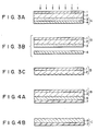
- Figs. 1A to 1C are sectional views showing a method of manufacturing a hologram stamper according to an embodiment of the present invention in an order of steps;
- Figs. 2A to 2C and 3A to 3C are sectional views showing methods of manufacturing a hologram stamper according to other embodiments of the present invention in orders of steps, respectively;
- Figs. 4A and 4B are sectional views showing a method of manufacturing a hologram by using the hologram stamper according to the present invention.
- reference numeral 1 denotes a film or sheet support; 2, a resin layer consisting of an electron beam-curable acrylate resin having a surface tension of 35 dyn/cm or more; 3, a photoresist layer on which a relief pattern as a hologram mother plate A is formed; and 4, a photoresist substrate.
- the substrate 4 is generally a glass plate.
- the film or sheet support 1 having an electron beam transparency must have, e.g., proper heat resistance, mechanical strength, and surface smoothness so that the support 1 can withstand heat applied on a thermoplastic resin of a hologram stamping resin plate in a post step and heat applied upon heat-press embossing.
- the material usable for the support 1 are polyester, polycarbonate, polyetherimide, polyphenylenesulfide, polyimide, polyetherketone, and glass.
- An aromatic polyester prepared by condensation of an aromatic dicarboxylic acid and bisphenol is most preferable in terms of an adhesion property with respect to the resin layer 3.
- the thickness of the support 1 is preferably 20 to 200 ⁇ m.
- an ester acrylate, epoxy acrylate, and urethane acrylate can be used as the electron beam-curable acrylate having a surface tension of 35 dyn/cm or more for use in the resin layer 2.
- an acrylate capable of forming a curable film which is of at least bifunctional and has a high crosslinking density is preferable.
- Examples of the acrylate are trimethylolpropanetriacrylate, ECH-modified ethyleneglycoldimethacrylate, PO,EO-modified bisphenol-A-diacrylate, EO-modified bisphenol-A-dimethacrylate, pentaerythritoltriacrylate, EO-modified phosphate diacrylate, ECH-modified glyceroltriacrylate, ECH-modified glyceroltriacrylate, ECH-modified phthalic diacrylate, and triallylisocyanurate, trimethylolpropane diacrylate, modified neopentylglycol. These compounds can be used in a combination of two or more thereof.
- the resin layer 2 can contain a polymerizable monomer having fluorine atoms in molecules in addition to the above acrylate resin.
- an acrylate resin having a low acidic value has a high miscibility. More specifically, the acid value is preferably 2.0 or less.
- the polymerizable monomer containing fluorine atoms in molecules preferably contains an acryloyl group as a radical polymerizable group.
- examples are 2,2,2-trifluoroethylacrylate, 2,2,2-trifluoroethylmethacrylate, undecafluorocyclohexylacrylate, nonafluorocyclopentylacrylate, pentadecafluorooctylmethacrylate, 2,3- bis(difluoroamino)propylacrylate, 2,2,2-trifluoro-1-(trifluoromethyl)ethylacrylate, 2,2-difluoro-2-nitroethylacrylate, 1,2,2,2-tetrafluoro-1-(trifluoromethyl)ethylacrylate, 2,2,3,3-tetrafluoro-3-(trifluoromethoxy)propylacrylate, 2,2,3,3,4,4,4-heptafluorobutylacrylate, 2,2,3,3,4,
- a mixing ratio between the electron beam- or ultraviolet rays-curable acrylate and the polymerizable monomer containing fluorine atoms in molecules in the resin layer 2 preferably falls within the range of 3 : 1 to 2 : 1 (weight ratio).
- the mixing ratio is not limited to this range since an optimal mixing ratio changes as, e.g., the type of material or a film or sheet substrate to be used is changed.
- the resin layer 2 may contain a thermosetting high-temperature resin in addition to the above acrylate resin.
- a thermosetting resin having good high-temperature properties to be used as the thermosetting high-temperature resin are a high-temperature epoxy resin, a high-temperature phenol resin, a melamine resin, a silicone resin, and a polyimide resin.
- a mixing ratio between the electron beam- or ultraviolet rays-curable acrylate and the thermosetting high-temperature resin preferably falls within the range of 1 : 10 to 1 : 4 (weight ratio).
- the mixing ratio is not limited to this range since an optimal mixing ratio changes as, e.g., the type of material, electron beam- or ultraviolet rays-curing conditions, or heat-curing conditions are changed.
- a positive resist having a high resolution is most preferable.
- a positive resist is commercially available as AZ-1350 or AZ-2400 (tradename: available from Cypray Co., Ltd.) or Way Coat HPR (tradename: Hunt Co., Ltd.)
- a glass plate is normally used as the photoresist substrate 4 because the substrate 4 requires a smoothness.
- an electron beam-curable acrylate resin having a surface tension of 35 dyn/cm or more is coated on the film or sheet support 1 by a known method such as knife coating, spin coating, bar coating or roll coating, thereby forming the resin layer 2.
- the resultant structure is then brought into contact with the surface of the photoresist 3 having a three-dimensional pattern of the hologram mother plate A.
- the photoresist 3 is coated on a 2- to 3-mm thick glass plate to have a film thickness of about 1 to 3 ⁇ m, exposed by an argon laser, and developed by a predetermined developing agent, thereby manufacturing a relief image.
- the resin layer is cured by radiating an electron beam or ultraviolet rays from the support 1 side and peeled from the surface of the hologram mother plate A, thereby obtaining a hologram stamper B constituted by the support and the cured resin layer as shown in Fig. 1C.
- an electron beam radiation amount is preferably 1.0 Mrad or more in order to sufficiently perform a curing reaction.
- a radiation amount is preferably 100 mJ/cm2 or more.
- Figs. 2A to 2C show another embodiment in which a structure obtained by forming a thin metal film 5 on the upper surface of a relief pattern 3 of a hologram mother plate is used as a hologram mother plate.
- examples of a material of the film 5 are aluminum, gold, silver, copper, tin, and alloys containing these metals.
- the conventional vacuum deposition method, sputtering method, ion plating method, or the like can be utilized as a film formation method.
- the film thickness preferably falls within the range of 100 to 10,000 ⁇ .
- a hologram stamper can be manufactured by the same method as shown in Figs. 1A to 1C.
- a resin solution containing an electron beam- or ultraviolet rays-curable resin or a monomer is coated on a support 1 by a known method such as knife coating, thereby forming a resin layer 2.
- the resultant structure is brought into contact with a thin metal film 5 of a hologram mother plate.
- the resin layer 2 is cured by radiating an electron beam or ultraviolet rays from the support 1 side and peeled from the surface of the thin metal film 5 of the hologram mother plate A.
- the resin layer is a mixture with a thermosetting resin
- the resin layer is further heated and completely cured after it is peeled.
- a hologram stamper B constituted by the support and the resin layer is obtained.
- Figs. 3A to 3C show still another embodiment of a method of manufacturing a hologram stamper.
- a resin layer 2 consisting of a resin solution containing an electron beam- or ultraviolet rays-curable resin or a monomer is coated on a support by a known method such as spin coating, bar coating, roll coating or knife coating.
- the resultant structure is brought into contact with the surface of a photoresist layer 3 of a hologram mother plate A, as shown in Fig. 1A (Fig. 3A).
- An electron beam or ultraviolet rays are radiated from the support 1 side to cure the resin layer 2.
- the resultant structure is subjected to peeling at the interface between the photoresist layer 3 and the substrate 4.
- a primer is preferably not used in the photoresist coating step.
- the photoresist layer 3 is then removed.
- a solvent which dissolves not the cured resin layer but only the photoresist layer 3 is selected, or the photoresist layer is exposed again and removed by a predetermined developing agent.
- a hologram stamper B consisting of the support and the resin layer is obtained as shown in Fig. 3C.
- the hologram stamper B obtained in any of the above embodiments is used in the manufacture of a hologram stamped product according to a method shown in Figs. 4A and 4B.
- the hologram stamped product B obtained in the above method is brought into contact with a thermoplastic resin layer 6, subjected to hot-press embossing, and then peeled from the layer 6, thereby manufacturing a hologram stamped product C as shown in Fig. 4B.
- reference numeral 6 denotes a thermoplastic resin layer; and 7, a substrate for the thermoplastic resin.
- the thermoplastic resin layer 6 may consist of, e.g., a polyester resin, polystyrene, a styrene-acryl copolymer, polyvinyl chloride, a polyvinyl acetate, a polyvinyl chloride-vinyl acetate copolymer, polyvinyl acetal, an alkyd resin resin, an acrylic resin, polyacrylonitrile, and polycarbonatepolyketone.
- the substrate 7 of the thermoplastic resin examples include polyester, polypropylene, polycarbonate, and cellophane.
- the electron beam- or ultraviolet rays-transmitting film can also be used.
- the film or sheet preferably has a thickness of about 10 to 100 ⁇ m.
- a MICROPOSIT 1350 (available from Cypray Co.) was used as a photoresist to form a photoresist layer having a film thickness of about 1.5 ⁇ m on a substrate consisting of a 3-mm thick glass plate.
- the surface tension was measured by an automatic surface tension meter (CBVP-A3 available from Kyowa Kaimen Kagaku K.K.)
- the resin solution layer was brought into contact with a relief surface of the hologram mother plate, and an electron beam of 200 keV was radqated at an absorbed dose of 5 Mrad from the support side.
- the resultant structure was peeled from the hologram mother plate to obtain a hologram stamper consisting of the support and the cured resin layer. Peeling between the cured resin layer and the photoresist as a hologram mother plate was good, i.e., a 90° peel strength was 5.2 g/cm.
- thermoplastic resin layer having the following composition was coated on a substrate consisting of a 50- ⁇ m thick polyester film to have a thickness of about 15 ⁇ m by using a wire bar, thereby manufacturing a hologram-reproducing film.
- DIANAL BR-101 (acrylic resin, available from Mitsubishi Rayon Co., Ltd.) 30 parts by weight Isopropanol 70 parts by weight
- the relief surface of the hologram stamper was brought into contact with the thermoplastic resin layer surface of the hologram-reproducing film at a pressure of about 25 kg/cm2 and heated at a temperature of 130°C for five seconds from the support surface of the hologram stamper. Thereafter, the thermoplastic resin layer surface was peeled from the hologram stamper to obtain a stamped hologram product. No blocking occurred upon peeling, and a hologram giving a good, sharp, and clear image was obtained.
- An electron beam-curable trimethylolpropanetriacrylate (KAYARAD TMPTA available from NIPPON KAYAKU CO., LTD.) having a surface tension of 37.0 dyn/cm was coated on a support consisting of a 75- ⁇ m thick polyimide film (UPILEX 75S, corona treatment grade, available from Ube Industries, Ltd.) to have a thickness of about 5 ⁇ m by using a wire bar, thereby forming a resin layer.
- UPILEX 75S corona treatment grade, available from Ube Industries, Ltd.
- a hologram stamper was manufactured following the same procedures as in Example-1. Peeling between the cured resin layer and the photoresist was good, i.e., a 90° peel strength was 3.5 g/cm.
- Example-1 Following the same procedures as in Example-1, a relief pattern was manufactured on a thermoplastic resin layer similar to that used in Example-1, thereby manufacturing a stamped hologram product. As a result, a clear hologram similar to that obtained in Example-1 was obtained.
- a hologram stamper was manufactured following the same procedures as in Example-1 except that a PO,EO-modified bisphenol-A-diacrylate (NK ester A-BPE-4, available from Shin Nakamura Kagaku K.K.) having a surface tension of 45.6 dyn/cm was used as an electron beam-curable resin. Peeling with respect to a photoresist mother plate was good, i.e., a 90° peel strength was 10.8 g/cm. In addition, a hot-press embossing suitability for a thermoplastic resin was excellent, and a good stamped hologram product as in Example-1 was obtained.
- a PO,EO-modified bisphenol-A-diacrylate NK ester A-BPE-4, available from Shin Nakamura Kagaku K.K.
- An electron beam was radiated to perform peeling following the same procedures as in Example-1 except that a neopentylglycoldiacrylate (KAYARAD NPGDA, available from NIPPON KAYAKU CO., LTD.) having a surface tension of 32.8 dyn/cm was used as an electron beam-curable resin. Since, however, an adhesion strength between the cured resin and a photoresist as a hologram mother plate was high, only a polyester film as a support was peeled.
- KAYARAD NPGDA available from NIPPON KAYAKU CO., LTD.
- KAYARAD MANDA An electron beam-curable hydroxy pivalic acid ester neopentylglycoldiacrylate (KAYARAD MANDA, available from NIPPON KAYAKU K.K.) having a surface tension of 34.2 dyn/cm was coated on a 75- ⁇ m thick polyimide film (UPILEX 75R, available from Ube Industries, Ltd.) to have a film thickness of about 5 ⁇ m by using a wire bar.
- UPILEX 75R available from Ube Industries, Ltd.
- An electron beam- or ultraviolet rays-curable solution mixture having the following composition was coated on a support consisting of a 70- ⁇ m thick polyester film by wire bar coating to have a film thickness of about 10 ⁇ m, thereby forming a resin layer.
- the resin layer was brought into contact with the relief surface of the hologram mother plate, and an electron beam of 200 keV was radiated at an absorbed dose of 4 Mrad from the support side. Thereafter, the resultant structure was peeled from the hologram mother plate to obtain a hologram stamper consisting of the support and the cured resin layer.
- Electron beam-curable trifunctional acrylate (KAYARAD TMPTA: available from NIPPON KAYAKU CO., LTD.) 70 parts by weight 2,2,2-trifluoroethylmethacrylate 30 parts by weight
- thermoplastic resin layer having the following composition was coated on a substrate consisting of a 50- ⁇ m thick polyester film by using a wire bar to have a thickness of about 15 ⁇ m, thereby manufacturing a hologram-reproducing film.
- DIANAL BR-101 available from Mitsubishi Rayon Co., Ltd. 40 parts by weight Isopropanol 60 parts by weight
- the relief surface of the hologram stamper was brought into contact with the thermoplastic resin layer surface of the hologram-reproducing film at a pressure of about 25 kg/cm2 and heated at a temperature of 130°C for five seconds from the support surface of the hologram stamper. Thereafter, the thermoplastic resin layer surface was peeled from the hologram stamper to obtain a stamped hologram product. No blocking or adhesion was found upon peeling, and a hologram giving a good, sharp, and clear image was obtained.
- a resin solution having the following composition was coated on a support consisting of a 100- ⁇ m thick polyester film by using a wire bar to have a thickness of about 10 ⁇ m, thereby forming a resin layer.
- a resin layer was brought into contact with the relief surface of a hologram mother plate following the same procedures as in Example-4, ultraviolet rays having an intensity of 400 mJ/cm2 were radiated from the support side to cure the resin layer. Thereafter, the cured resin layer was peeled to manufacture a hologram stamper.
- Ultraviolet rays-curable bifunctional acrylate (KAYARAD R-604: available from NIPPON KAYAKU CO., LTD.) 40 parts by weight Ultraviolet rays-curable oligomer (Trimethylolpropane diacrylate, modified neopentylglycol) (KAYARAD HX-220: available from NIPPON KAYAKU CO., LTD.) 25 parts by weight Pentadecafluorooctyl methacrylate 35 parts by weight Benzoinisobutylether 0.4 parts by weight
- Example-4 Following the same procedures as in Example-4, a relief pattern was formed on a thermoplastic resin layer similar to that used in Example-4, thereby manufacturing a stamped hologram product. As a result, a clear hologram as in Example-4 was obtained.
- a relief hologram was manufactured following the same procedures as in Example-4 to be used as a hologram mother plate.
- a solution mixture of an electron beam-curable acrylate resin and a thermosetting high-temperature resin having the following compositions was coated on a support consisting of a 75- ⁇ m thick polyimide film (UPILEX 75S, available from Ube Industries, Ltd.) by wire bar coating to have a thickness of about 10 ⁇ m, and soft baking for removing a solvent was performed at 80°C for one minute and at 100°C for five minutes, thereby forming a resin layer.
- the resin layer was brought into contact with the relief surface of the hologram mother plate and irradiated with an electron beam of 200 keV at an absorbed dose of 5 Mrad from the support side.
- Electron beam-curable bifunctional acrylate (KAYARAD R-604: available from NIPPON KAYAKU CO., LTD.) 15 parts by weight
- Thermosetting resin Trimethylolpropane diacrylate, modified neopentylglycol
- BILALIN PI-2555 available from Du Pont de Nemours, E.I., Co.
- thermoplastic resin having the following composi tion was coated on a substrate consisting of a 50- ⁇ m thick polyester film by using a wire bar to have a thickness of about 15 ⁇ m, thereby manufacturing a stamped hologram film.
- DIANAL BR-101 available from Mitsubishi Rayon Co., Ltd. 40 parts by weight Isopropanol 60 parts by weight
- the relief surface of the hologram stamper was brought into contact with the thermoplastic resin layer surface of the stamped hologram film at a pressure of about 25 kg/cm2 and heated at 130°C for five seconds from the support surface of the hologram stamper. Thereafter, the thermoplastic layer surface was peeled from the hologram stamper to obtain a hologram stamped product. As a result, a hologram giving a good, sharp, and clear image was obtained.
- a solution mixture of ultraviolet rays-curable acrylate and a thermosetting high-temperature resin having the following compositions was coated on a support consisting of a 100- ⁇ m thick polyester film by using a wire bar to have a thickness of about 10 ⁇ m, and soft baking for removing a solvent was performed at 80°C for five minutes, thereby forming a resin layer.
- the resin layer was brought into contact with the relief surface of a hologram mother plate, and irradiated and precured by ultraviolet rays having an intensity of 500 mJ/cm2 from the support side.
- the precured resin layer was peeled from the hologram stamper, and heated and completely cured at 180°C for one hour, thereby manufacturing a hologram stamping resin plate.
- Ultraviolet rays-curable trifunctional acrylate (KAYARAD TMPTA: available from NIPPON KAYAKU CO., LTD.) 10 parts by weight Thermosetting resin (polyimide) (CHEMITITE CT410: available from TOSHIBA CHEMICAL CORP.) 90 parts by weight Benzoinisobutylether 0.4 parts by weight
- Example-6 Following the same procedures as in Example-6, a relief pattern was formed on a thermoplastic resin layer to obtain a hologram stamped product. As a result, a clear hologram similar to that in Example-6 was obtained.
- Neopentylglycol-modified trimethylolprapanediacrylate as an electron beam-curable acrylate was coated on a support consisting of a 70- ⁇ m thick aromatic polyester film by wire bar coating to have a film thickness of about 5 ⁇ m, thereby forming a resin solution layer.
- the resin solution layer was brought into contact with the relief surface of the grating used instead of a hologram mother plate and irradiated with an electron beam of 200 keV at an absorbed dose of seven Hrad from the support side. Thereafter, the resin layer was peeled from the hologram mother plate to obtain a hologram stamper constituted by the support and the cured resin layer. A peeling properly between the cured resin layer and the photoresist was good.
- thermoplastic resin layer having the following composition was coated on a substrate consisting of a 50- ⁇ m thick polyester film by using a wire bar to have a thickness of about 15 ⁇ m, thereby manufacturing a stamped hologram film.
- DIANAL BR-101 available from Mitsubishi Rayon Co., Ltd. 40 parts by weight Isopropanol 60 parts by weight
- the relief surface of the hologram stamper was brought into contact with the thermoplastic layer surface of the stamped hologram film at a pressure of about 40 kg/cm2 and heated at 160°C for three seconds from the support surface of the hologram stamper. Thereafter, the thermoplastic resin layer surface was peeled from the hologram stamper to obtain a stamped hologram product. After a similar hot-press emboss-stamping step was repeated 100 times, the stamper remained unchanged, and a stamped product giving clear and sharp diffracted light was obtained.
- An electron beam-curable acrylate having the following composition was coated on a support consisting of a 100- ⁇ m thick aromatic polyester film by using a wire bar to have a film thickness of about 5 ⁇ m, thereby forming a resin layer. Thereafter, a hologram stamper was manufactured following the same procedures as in
- a relief pattern was formed on a thermoplastic resin layer similar to that used in Example-8 following the same procedures as in Example-8, thereby manufacturing a stamped product. As in Example-8, after stamping was performed 100 times, a stamped product giving clear diffracted light was obtained.
- AZ-1350 (available from Cypray Co.) was used as a photoresist to form a photoresist layer having a film thickness of about 1.5 ⁇ m on a substrate consisting of a 3-mm thick glass plate.
- the resultant structure was dried, and a thin Al film having a film thickness of about 1,000 ⁇ was formed on the relief surface by a vacuum deposition method to be used as a hologram mother plate.
- An electron beam- or ultraviolet rays-curable resin having the following composition was coated on a support consisting of a 70- ⁇ m thick polyester film by wire bar coating to have a film thickness of about 10 ⁇ m, thereby forming a resin layer.
- the resin layer was brought into contact with the Al-deposited surface of the hologram mother plate and irradiated with an electron beam of 200 keV at an absorbed dose of 5 Mrad from the support side, thereby manufacturing a hologram stamper consisting of the hologram film and the cured resin.
- a peeling property between the hologram mother plate and the resin layer was good.
- Electron beam-curable bifunctional acrylate monomer (KAYARAD MANDA: available from NIPPON KAYAKU CO., LTD.) 60 parts by weight
- Electron beam-curable bifunctional urethaneacrylate oligomer (NK ester u-108-A: available from Shin Nakamura Kagaku K.K.) 40 parts by weight
- thermoplastic resin having the following composition was coated on a support consisting of a 50- ⁇ m thick polyester film by using a wire bar to have a thickness of about 15 ⁇ m, thereby manufacturing a stamped hologram film.
- DIANAL BR-101 available from Mitsubishi Rayon Co., Ltd. 40 parts by weight Isopropanol 60 parts by weight
- thermoplastic layer surface The relief surface of a hologram stamping resin plate was brought into contact with the thermoplastic layer surface at a pressure of about 25 kg/cm2 and heated at 130°C for five seconds from the support surface of the hologram stamper. Thereafter, the thermoplastic resin layer surface was peeled from the hologram stamper to obtain a stamped hologram. As a result, a hologram giving a good, sharp, and clear image was obtained.
- a hologram stamper was manufactured following the same procedures as in Example-10 except that an electron beam- or ultraviolet rays-curable resin solution was directly brought into contact with the relief surface of a photoresist layer without forming an Al-deposited film on the relief surface of a hologram mother plate.
- the resin layer was cured by electron beam radiation and peeled from the surface of the photopolymer as a hologram mother plate. Since, however, a cohesive failure occurred from inside the photopolymer layer or peeling was produced from the photopolymer substrate surface, no practical hologram stamper could be obtained.
- AZ-1350 (available from Cypray Co.) was used as a photoresist to form a photoresist layer having a film thickness of about 1.5 ⁇ m on a substrate consisting of a 3-mm thick glass plate without using a primer.
- An electron beam-curable resin having the following composition was coated on a support consisting of a 70- ⁇ m thick polyester film by wire bar coating to have a film thickness of about 10 ⁇ m, thereby forming a resin layer.
- the resin layer was brought into contact with the relief surface of the hologram mother plate and irradiated with an electron beam of 200 keV at an absorbed dose of 5 Mrad from the support side.
- the resultant structure was peeled at the interface between the photoresist layer and the glass plate as a substrate of the hologram mother plate.
- the photoresist layer was exposed by ultraviolet rays and removed in an alkali developing agent by an ultrasolic wave, thereby manufacturing a hologram stamper consisting of the polyester film and the cured resin.
- Electron beam-curable difunctional acrylate (NK ester A-BPE-4, PO,EO-modified bisphenol-A-diacrylate, available from Shin Nakamura Kagaku K.K.) 70 parts by weight
- Electron beam-curable urethaneacrylate (NK ester u-108-A: available from Shin Nakamura Kagaku K.K.) 30 parts by weight
- thermoplastic resin having the following composition was coated on a support consisting of a 50- ⁇ m thick polyester film by using a wire bar to have a thickness of about 15 ⁇ m, thereby manufacturing a stamped hologram film.
- DIANAL BR-101 available from Mitsubishi Rayon Co., Ltd. 40 parts by weight Isopropanol 60 parts by weight
- the relief surface of the hologram stamper was brought into contact with the thermoplastic resin layer surface of the stamped hologram film at a pressure of about 25 kg/cm2 and heated at 120°C for five seconds from the support side of the hologram stamper. Thereafter, the thermoplastic resin layer surface was peeled from the hologram stamper to obtain a hologram stamped product. As a result, a hologram giving a good, sharp, and clear image was obtained.
- a resin solution having the following composition was coated on a support consisting of a 100- ⁇ m thick polyester film by using a wire bar to have a film thickness of about 10 ⁇ m and brought into contact with the relief surface of a hologram mother plate.
- the resin layer was cured by radiating ultraviolet rays having an intensity of 400 mJ/cm2 from the polyester film side, and the photoresist layer was removed, thereby manufacturing a hologram stamper.
- the obtained stamper was good as that obtained in Example-11.
- Ultraviolet rays-curable bifunctional acrylate (KAYARAD MANDA: available from NIPPON KAYAKU CO., LTD.) 70 parts by weight
- Ultraviolet rays-curable oligomer (KAYARAD HX-220: available from NIPPON KAYAKU CO., LTD.) 30 parts by weight Benzoinisobutylether 0.4 parts by weight
- Example-11 A relief pattern was formed on the thermoplastic resin layer following the same procedures as in Example-11, thereby manufacturing a hologram stamped product. As a result, a clear hologram as in Example-11 was obtained.
- a relief type hologram stamper (B) which comprises as a hologram relief pattern formation layer a resin layer (2) comprising an electron beam- or ultraviolet rays-curable acrylate resin having a surface tension of not less than 35 dyn/cm, and formed on an electron beam-or ultraviolet rays-transmitting film or sheet support (1).
- a fine relief pattern can be formed on the surface of the resin layer (2) by pressing a hologram mother (A) plate having a fine relief pattern (3) onto the surface of the resin layer (2) and subsequently irradiating an electron beam or ultraviolet rays to cure the resin layer (2).
- This stamper (B) is used to form a hologram on a substrate having a thermoplastic resin surface layer by means of a hot pressing method.
Abstract
Description
- The present invention relates to the manufacture of a hologram and, more particularly, to a relief type hologram stamper and a method of manufacturing the same and a method of efficiently manufacturing a hologram.
- A hologram for reproducing a three-dimensional image has a good artistic design and is therefore used as cover pages of, e.g., books and magazines, POP displays, gifts, and the like. In addition, since a hologram is equivalent to recording information of the order of submicrons, it is used to prevent forgery of securities, credit cards, and the like.
- In order to mass-produce a relief type hologram, a die manufactured by metal plating or the like from a photoresist on which an embossed relief pattern is formed is generally used as a mother plate to hot-press mold a thermoplastic resin coated on a substrate, thereby manufacturing a large number of holograms. In this method, however, since the die requires a large number of manufacturing steps, it is difficult to control quality, and much time and many labors are necessary, resulting in an expensive product.
- In order to solve the above problem, therefore, Published Unexamined Japanese Patent Application No. 58-184986 discloses a method in which an electron beam- or ultraviolet rays-curable resin, a thermoplastic resin, or a thermosetting resin is used as a stamper instead of a die. In this method, upon manufacture of a resin plate, an electron beam- or ultraviolet rays-curable resin is directly brought into contact with the surface of a photopolymer as a mother plate to form a relief pattern. In this case, in order to precisely reproduce a relief pattern of a hologram mother plate, a wetting property between the photopolymer and the curable resin must be excellent. Since, however, an adhesion strength between the photopolymer and the curable resin is increased as the wetting property is improved, it is practically very difficult to peel an initial relief pattern while keeping it in good conditions. Even if the relief pattern is peeled, the relief pattern cannot be prevented from being damaged by a cohesive failure or the like in the photopolymer or curable resin. In addition, the type of curable resin useful therefor is very strictly limited.
- In the invention disclosed in Published Unexamined Japanese Patent Application No. 58-184986 described above, upon manufacture of a stamper hologram using a resin plate, an electron beam- or ultraviolet rays-curable resin is brought into contact with the resin plate, and is cured and shaped by electron beam or ultraviolet rays radiation. Therefore, since the resin plate itself may be degraded upon repetitive radiation of high-energy rays, it is difficult to maintain stable quality.
- It is an object of the present invention to use an electron beam- or ultraviolet rays-curable resin as a hologram relief pattern formation layer, thereby reducing the number of hologram stamper manufacturing steps and saving a time required for the manufacturing steps.
- It is another object of the present invention to provide a method, based on hot-press embossing which is simple in principle, for manufacturing a large number of holograms having a clear image and stable quality on a thermoplastic resin within a short time period.
- In order to achieve the above objects, the present inventors have made extensive studies and attained the present invention in which a resin layer containing an electron beam- or ultraviolet rays-curable acrylate resin having a surface tension of 35 dyn/cm or more is used as a relief pattern formation layer so that the relief pattern formation layer can be easily peeled from a mother plate, and this relief pattern formation layer is used as a stamper to reduce the number of stamper manufacturing steps and stabilize product quality.
- That is, according to the present invention, there is provided a hologram stamper comprising: a resin layer comprising an electron beam- or ultraviolet rays-curable acrylate resin having a surface tension of 35 dyn/cm or more, and preferably, 35 to 55 dyn/cm, and formed on an electron beam- or ultraviolet rays-transmitting film or sheet support; and a fine relief pattern formed on the surface of the resin layer, wherein the relief pattern is cured by an electron beam or ultraviolet rays.
- In addition, according to the present invention, there is provided a method of manufacturing a hologram stamper, comprising the steps of: forming a resin layer comprising a resin containing at least an electron beam- or ultraviolet rays-curable resin or a monomer, and having a surface tension of 35 dyn/cm or more, on an electron beam- or ultraviolet rays-transmitting film or sheet support; bringing a hologram mother plate having a fine relief pattern into contact with the resin layer; irradiating an electron beam or ultraviolet rays to cure the resin layer; and peeling the resin layer from the hologram mother plate.
- Note that the above relief pattern formation resin layer may further contain, in addition to the acrylate resin, a polymerizable monomer containing fluorine atoms in molecules or a thermosetting resin.
- The above acrylate resin is preferably, e.g., an ester acrylate, epoxy acrylate, or urethane acrylate containing at least two acryloyl group in one molecule.
- Although the electron beam- or ultraviolet rays-transmitting support is not particularly limited, an aromatic polyester film or sheet is preferably used in view of its excellent adhesion property with respect to the resin layer.
- When a thermosetting resin is contained as the resin layer, a two-step curing method is preferably adopted. That is, in the two-step curing method, a resin layer is brought into contact with a hologram mother plate, irradiated and precured by an electron beam or ultraviolet rays, peeled from the hologram mother plate, and then heated and completely cured.
- Note that the above resin layer may further contain a thermoplastic resin.
- The hologram mother plate may be manufactured by coating a thin metal film on a hologram relief pattern. Alternatively, the hologram mother plate may be manufactured by forming a peelable photoresist layer on a substrate, curing a resin layer by an electron beam or the like, peeling the resin layer from the substrate together with the photoresist layer, and then dissolving and removing only the photoresist layer by a solvent.
- This invention can be more fully understood from the following detailed description when taken in conjunction with the accompanying drawings, in which:
- Figs. 1A to 1C are sectional views showing a method of manufacturing a hologram stamper according to an embodiment of the present invention in an order of steps;
- Figs. 2A to 2C and 3A to 3C are sectional views showing methods of manufacturing a hologram stamper according to other embodiments of the present invention in orders of steps, respectively; and
- Figs. 4A and 4B are sectional views showing a method of manufacturing a hologram by using the hologram stamper according to the present invention.
- Embodiments of the present invention will be described in detail below with reference to the accompanying drawings.
- Referring to Fig. 1, reference numeral 1 denotes a film or sheet support; 2, a resin layer consisting of an electron beam-curable acrylate resin having a surface tension of 35 dyn/cm or more; 3, a photoresist layer on which a relief pattern as a hologram mother plate A is formed; and 4, a photoresist substrate. The
substrate 4 is generally a glass plate. - In the present invention, the film or sheet support 1 having an electron beam transparency must have, e.g., proper heat resistance, mechanical strength, and surface smoothness so that the support 1 can withstand heat applied on a thermoplastic resin of a hologram stamping resin plate in a post step and heat applied upon heat-press embossing. More specifically, examples of the material usable for the support 1 are polyester, polycarbonate, polyetherimide, polyphenylenesulfide, polyimide, polyetherketone, and glass. An aromatic polyester prepared by condensation of an aromatic dicarboxylic acid and bisphenol is most preferable in terms of an adhesion property with respect to the
resin layer 3. Normally, the thickness of the support 1 is preferably 20 to 200 µm. - As the electron beam-curable acrylate having a surface tension of 35 dyn/cm or more for use in the
resin layer 2, an ester acrylate, epoxy acrylate, and urethane acrylate can be used. In this case, an acrylate capable of forming a curable film which is of at least bifunctional and has a high crosslinking density is preferable. Examples of the acrylate are trimethylolpropanetriacrylate, ECH-modified ethyleneglycoldimethacrylate, PO,EO-modified bisphenol-A-diacrylate, EO-modified bisphenol-A-dimethacrylate, pentaerythritoltriacrylate, EO-modified phosphate diacrylate, ECH-modified glyceroltriacrylate, ECH-modified glyceroltriacrylate, ECH-modified phthalic diacrylate, and triallylisocyanurate, trimethylolpropane diacrylate, modified neopentylglycol. These compounds can be used in a combination of two or more thereof. - The
resin layer 2 can contain a polymerizable monomer having fluorine atoms in molecules in addition to the above acrylate resin. In this case, an acrylate resin having a low acidic value has a high miscibility. More specifically, the acid value is preferably 2.0 or less. - The polymerizable monomer containing fluorine atoms in molecules preferably contains an acryloyl group as a radical polymerizable group. Examples are 2,2,2-trifluoroethylacrylate,
2,2,2-trifluoroethylmethacrylate,
undecafluorocyclohexylacrylate,
nonafluorocyclopentylacrylate,
pentadecafluorooctylmethacrylate,
2,3- bis(difluoroamino)propylacrylate,
2,2,2-trifluoro-1-(trifluoromethyl)ethylacrylate,
2,2-difluoro-2-nitroethylacrylate,
1,2,2,2-tetrafluoro-1-(trifluoromethyl)ethylacrylate,
2,2,3,3-tetrafluoro-3-(trifluoromethoxy)propylacrylate, 2,2,3,3,4,4,4-heptafluorobutylacrylate,
2,2,3,3,4,4-hexafluoro-1,5-pentadiilacrylate. - A mixing ratio between the electron beam- or ultraviolet rays-curable acrylate and the polymerizable monomer containing fluorine atoms in molecules in the
resin layer 2 preferably falls within the range of 3 : 1 to 2 : 1 (weight ratio). The mixing ratio, however, is not limited to this range since an optimal mixing ratio changes as, e.g., the type of material or a film or sheet substrate to be used is changed. - The
resin layer 2 may contain a thermosetting high-temperature resin in addition to the above acrylate resin. In this case, examples of a thermosetting resin having good high-temperature properties to be used as the thermosetting high-temperature resin are a high-temperature epoxy resin, a high-temperature phenol resin, a melamine resin, a silicone resin, and a polyimide resin. - A mixing ratio between the electron beam- or ultraviolet rays-curable acrylate and the thermosetting high-temperature resin preferably falls within the range of 1 : 10 to 1 : 4 (weight ratio). The mixing ratio, however, is not limited to this range since an optimal mixing ratio changes as, e.g., the type of material, electron beam- or ultraviolet rays-curing conditions, or heat-curing conditions are changed.
- Although a generally, widely used semiconductor resist can be used as the
photoresist layer 3 on which a relief pattern of the hologram mother plate A is formed, a positive resist having a high resolution is most preferable. Such a positive resist is commercially available as AZ-1350 or AZ-2400 (tradename: available from Cypray Co., Ltd.) or Way Coat HPR (tradename: Hunt Co., Ltd.) A glass plate is normally used as thephotoresist substrate 4 because thesubstrate 4 requires a smoothness. - Steps of manufacturing a hologram stamper will be described below.
- First, in Fig. 1A, an electron beam-curable acrylate resin having a surface tension of 35 dyn/cm or more is coated on the film or sheet support 1 by a known method such as knife coating, spin coating, bar coating or roll coating, thereby forming the
resin layer 2. The resultant structure is then brought into contact with the surface of thephotoresist 3 having a three-dimensional pattern of the hologram mother plate A. - The
photoresist 3 is coated on a 2- to 3-mm thick glass plate to have a film thickness of about 1 to 3 µm, exposed by an argon laser, and developed by a predetermined developing agent, thereby manufacturing a relief image. - As shown in Fig. 1B, the resin layer is cured by radiating an electron beam or ultraviolet rays from the support 1 side and peeled from the surface of the hologram mother plate A, thereby obtaining a hologram stamper B constituted by the support and the cured resin layer as shown in Fig. 1C. In this case, an electron beam radiation amount is preferably 1.0 Mrad or more in order to sufficiently perform a curing reaction. In the case of ultraviolet rays, a radiation amount is preferably 100 mJ/cm² or more.
- Figs. 2A to 2C show another embodiment in which a structure obtained by forming a thin metal film 5 on the upper surface of a
relief pattern 3 of a hologram mother plate is used as a hologram mother plate. In this case, examples of a material of the film 5 are aluminum, gold, silver, copper, tin, and alloys containing these metals. The conventional vacuum deposition method, sputtering method, ion plating method, or the like can be utilized as a film formation method. The film thickness preferably falls within the range of 100 to 10,000 Å. - In this embodiment, a hologram stamper can be manufactured by the same method as shown in Figs. 1A to 1C.
- That is, as shown in Fig. 2A, a resin solution containing an electron beam- or ultraviolet rays-curable resin or a monomer is coated on a support 1 by a known method such as knife coating, thereby forming a
resin layer 2. The resultant structure is brought into contact with a thin metal film 5 of a hologram mother plate. - As shown in Fig. 2B, the
resin layer 2 is cured by radiating an electron beam or ultraviolet rays from the support 1 side and peeled from the surface of the thin metal film 5 of the hologram mother plate A. When the resin layer is a mixture with a thermosetting resin, the resin layer is further heated and completely cured after it is peeled. As a result, as shown in Fig. 2C, a hologram stamper B constituted by the support and the resin layer is obtained. - Figs. 3A to 3C show still another embodiment of a method of manufacturing a hologram stamper. First, a
resin layer 2 consisting of a resin solution containing an electron beam- or ultraviolet rays-curable resin or a monomer is coated on a support by a known method such as spin coating, bar coating, roll coating or knife coating. The resultant structure is brought into contact with the surface of aphotoresist layer 3 of a hologram mother plate A, as shown in Fig. 1A (Fig. 3A). An electron beam or ultraviolet rays are radiated from the support 1 side to cure theresin layer 2. - As shown in Fig. 3B, the resultant structure is subjected to peeling at the interface between the
photoresist layer 3 and thesubstrate 4. In order to improve a peeling property, a primer is preferably not used in the photoresist coating step. Thephotoresist layer 3 is then removed. In this case, a solvent which dissolves not the cured resin layer but only thephotoresist layer 3 is selected, or the photoresist layer is exposed again and removed by a predetermined developing agent. As a result, a hologram stamper B consisting of the support and the resin layer is obtained as shown in Fig. 3C. - The hologram stamper B obtained in any of the above embodiments is used in the manufacture of a hologram stamped product according to a method shown in Figs. 4A and 4B.
- That is, as shown in Fig. 4A, the hologram stamped product B obtained in the above method is brought into contact with a
thermoplastic resin layer 6, subjected to hot-press embossing, and then peeled from thelayer 6, thereby manufacturing a hologram stamped product C as shown in Fig. 4B. - Note that in Figs. 4A and 4B,
reference numeral 6 denotes a thermoplastic resin layer; and 7, a substrate for the thermoplastic resin. - The
thermoplastic resin layer 6 may consist of, e.g., a polyester resin, polystyrene, a styrene-acryl copolymer, polyvinyl chloride, a polyvinyl acetate, a polyvinyl chloride-vinyl acetate copolymer, polyvinyl acetal, an alkyd resin resin, an acrylic resin, polyacrylonitrile, and polycarbonatepolyketone. - Examples of the
substrate 7 of the thermoplastic resin are polyester, polypropylene, polycarbonate, and cellophane. The electron beam- or ultraviolet rays-transmitting film can also be used. In this case, the film or sheet preferably has a thickness of about 10 to 100 µm. - The present invention will be described in more detail below by way of its examples.
- A MICROPOSIT 1350 (available from Cypray Co.) was used as a photoresist to form a photoresist layer having a film thickness of about 1.5 µm on a substrate consisting of a 3-mm thick glass plate. An interference fringe of a three-dimensional object was exposed by an argon laser (wavelength = 457.9 nmqand intensity = 50 mJ/cm2) for about 10 minutes, and a relief hologram was manufactured by alkali development, thereby obtaining a hologram mother plate.
- An electron beam-curable ECH-modified ethyleneglycoldimethacrylate (DENACOL DM-811 available from NAGASE & CO., LTD.) having a surface tension of 41.4 dyn/cm was coated on a support consisting of a 70-µm thick polyester film to have a film thickness of about 5 µm by wire bar coating, thereby forming a resin solution layer. The surface tension was measured by an automatic surface tension meter (CBVP-A3 available from Kyowa Kaimen Kagaku K.K.) The resin solution layer was brought into contact with a relief surface of the hologram mother plate, and an electron beam of 200 keV was radqated at an absorbed dose of 5 Mrad from the support side. Thereafter, the resultant structure was peeled from the hologram mother plate to obtain a hologram stamper consisting of the support and the cured resin layer. Peeling between the cured resin layer and the photoresist as a hologram mother plate was good, i.e., a 90° peel strength was 5.2 g/cm.
- A thermoplastic resin layer having the following composition was coated on a substrate consisting of a 50-µm thick polyester film to have a thickness of about 15 µm by using a wire bar, thereby manufacturing a hologram-reproducing film.
DIANAL BR-101 (acrylic resin, available from Mitsubishi Rayon Co., Ltd.) 30 parts by weight Isopropanol 70 parts by weight - The relief surface of the hologram stamper was brought into contact with the thermoplastic resin layer surface of the hologram-reproducing film at a pressure of about 25 kg/cm² and heated at a temperature of 130°C for five seconds from the support surface of the hologram stamper. Thereafter, the thermoplastic resin layer surface was peeled from the hologram stamper to obtain a stamped hologram product. No blocking occurred upon peeling, and a hologram giving a good, sharp, and clear image was obtained.
- An electron beam-curable trimethylolpropanetriacrylate (KAYARAD TMPTA available from NIPPON KAYAKU CO., LTD.) having a surface tension of 37.0 dyn/cm was coated on a support consisting of a 75-µm thick polyimide film (UPILEX 75S, corona treatment grade, available from Ube Industries, Ltd.) to have a thickness of about 5 µm by using a wire bar, thereby forming a resin layer. Thereafter, a hologram stamper was manufactured following the same procedures as in Example-1. Peeling between the cured resin layer and the photoresist was good, i.e., a 90° peel strength was 3.5 g/cm.
- Following the same procedures as in Example-1, a relief pattern was manufactured on a thermoplastic resin layer similar to that used in Example-1, thereby manufacturing a stamped hologram product. As a result, a clear hologram similar to that obtained in Example-1 was obtained.
- A hologram stamper was manufactured following the same procedures as in Example-1 except that a PO,EO-modified bisphenol-A-diacrylate (NK ester A-BPE-4, available from Shin Nakamura Kagaku K.K.) having a surface tension of 45.6 dyn/cm was used as an electron beam-curable resin. Peeling with respect to a photoresist mother plate was good, i.e., a 90° peel strength was 10.8 g/cm. In addition, a hot-press embossing suitability for a thermoplastic resin was excellent, and a good stamped hologram product as in Example-1 was obtained.
- An electron beam was radiated to perform peeling following the same procedures as in Example-1 except that a neopentylglycoldiacrylate (KAYARAD NPGDA, available from NIPPON KAYAKU CO., LTD.) having a surface tension of 32.8 dyn/cm was used as an electron beam-curable resin. Since, however, an adhesion strength between the cured resin and a photoresist as a hologram mother plate was high, only a polyester film as a support was peeled.
- An electron beam-curable hydroxy pivalic acid ester neopentylglycoldiacrylate (KAYARAD MANDA, available from NIPPON KAYAKU K.K.) having a surface tension of 34.2 dyn/cm was coated on a 75-µm thick polyimide film (UPILEX 75R, available from Ube Industries, Ltd.) to have a film thickness of about 5 µm by using a wire bar.
- An electron beam was radiated following the same procedures as in Example-1, and then peeling was performed.
- As in Comparative Example-1, however, since an adhesion strength between a cured resin and a photoresist was high, the resultant structure was peeled from the surface of glass as a photoresist substrate. The above results are summarized in Table 1 below.
Table 1 Surface Tension (dyn/cm) Peel Strength (g/cm) Peeling State Example-1 41.4 5.2 good Example-2 37.0 3.5 good Example-3 45.6 10.8 good Comparative Example-1 32.8 Unmeasurable Only Support Was Peeled Comparative Example-2 34.2 Unmeasurable Peeled From Substrate Surface - AZ-1350 (Cypray Co.) was used as a photoresist to form a 1.5-µm thick photoresist layer on a substrate consisting of a 3-mm thick glass plate, and an interfer ence fringe of a three-dimensional object was exposed by an argon laser (wavelength = 457.9 nm and intensity = 50 mJ/cm²) for about 10 minutes. Thereafter, a relief hologram was manufactured by alkali development to be used as a hologram mother plate.
- An electron beam- or ultraviolet rays-curable solution mixture having the following composition was coated on a support consisting of a 70-µm thick polyester film by wire bar coating to have a film thickness of about 10 µm, thereby forming a resin layer. The resin layer was brought into contact with the relief surface of the hologram mother plate, and an electron beam of 200 keV was radiated at an absorbed dose of 4 Mrad from the support side. Thereafter, the resultant structure was peeled from the hologram mother plate to obtain a hologram stamper consisting of the support and the cured resin layer.
Electron beam-curable trifunctional acrylate (KAYARAD TMPTA: available from NIPPON KAYAKU CO., LTD.) 70 parts by weight 2,2,2-trifluoroethylmethacrylate 30 parts by weight - A thermoplastic resin layer having the following composition was coated on a substrate consisting of a 50-µm thick polyester film by using a wire bar to have a thickness of about 15 µm, thereby manufacturing a hologram-reproducing film.
DIANAL BR-101 (available from Mitsubishi Rayon Co., Ltd.) 40 parts by weight Isopropanol 60 parts by weight - The relief surface of the hologram stamper was brought into contact with the thermoplastic resin layer surface of the hologram-reproducing film at a pressure of about 25 kg/cm² and heated at a temperature of 130°C for five seconds from the support surface of the hologram stamper. Thereafter, the thermoplastic resin layer surface was peeled from the hologram stamper to obtain a stamped hologram product. No blocking or adhesion was found upon peeling, and a hologram giving a good, sharp, and clear image was obtained.
- A resin solution having the following composition was coated on a support consisting of a 100-µm thick polyester film by using a wire bar to have a thickness of about 10 µm, thereby forming a resin layer. After the resin layer was brought into contact with the relief surface of a hologram mother plate following the same procedures as in Example-4, ultraviolet rays having an intensity of 400 mJ/cm² were radiated from the support side to cure the resin layer. Thereafter, the cured resin layer was peeled to manufacture a hologram stamper.
Ultraviolet rays-curable bifunctional acrylate (KAYARAD R-604: available from NIPPON KAYAKU CO., LTD.) 40 parts by weight Ultraviolet rays-curable oligomer (Trimethylolpropane diacrylate, modified neopentylglycol) (KAYARAD HX-220: available from NIPPON KAYAKU CO., LTD.) 25 parts by weight Pentadecafluorooctyl methacrylate 35 parts by weight Benzoinisobutylether 0.4 parts by weight - Following the same procedures as in Example-4, a relief pattern was formed on a thermoplastic resin layer similar to that used in Example-4, thereby manufacturing a stamped hologram product. As a result, a clear hologram as in Example-4 was obtained.
- A relief hologram was manufactured following the same procedures as in Example-4 to be used as a hologram mother plate.
- A solution mixture of an electron beam-curable acrylate resin and a thermosetting high-temperature resin having the following compositions was coated on a support consisting of a 75-µm thick polyimide film (UPILEX 75S, available from Ube Industries, Ltd.) by wire bar coating to have a thickness of about 10 µm, and soft baking for removing a solvent was performed at 80°C for one minute and at 100°C for five minutes, thereby forming a resin layer. The resin layer was brought into contact with the relief surface of the hologram mother plate and irradiated with an electron beam of 200 keV at an absorbed dose of 5 Mrad from the support side. Thereafter, the resultant resin layer was peeled from the relief surface of the hologram mother plate to form a hologram prestamper consisting of the support and the precured resin. This prestamper was heated and completely cured at 300°C for 90 minutes, thereby manufacturing a hologram stamper.
Electron beam-curable bifunctional acrylate (KAYARAD R-604: available from NIPPON KAYAKU CO., LTD.) 15 parts by weight Thermosetting resin (Trimethylolpropane diacrylate, modified neopentylglycol) (BILALIN PI-2555: available from Du Pont de Nemours, E.I., Co.) 90 parts by weight - A thermoplastic resin having the following composi tion was coated on a substrate consisting of a 50-µm thick polyester film by using a wire bar to have a thickness of about 15 µm, thereby manufacturing a stamped hologram film.
DIANAL BR-101 (available from Mitsubishi Rayon Co., Ltd.) 40 parts by weight Isopropanol 60 parts by weight - The relief surface of the hologram stamper was brought into contact with the thermoplastic resin layer surface of the stamped hologram film at a pressure of about 25 kg/cm² and heated at 130°C for five seconds from the support surface of the hologram stamper. Thereafter, the thermoplastic layer surface was peeled from the hologram stamper to obtain a hologram stamped product. As a result, a hologram giving a good, sharp, and clear image was obtained.
- A solution mixture of ultraviolet rays-curable acrylate and a thermosetting high-temperature resin having the following compositions was coated on a support consisting of a 100-µm thick polyester film by using a wire bar to have a thickness of about 10 µm, and soft baking for removing a solvent was performed at 80°C for five minutes, thereby forming a resin layer. Following the same procedures as in Example-6, the resin layer was brought into contact with the relief surface of a hologram mother plate, and irradiated and precured by ultraviolet rays having an intensity of 500 mJ/cm² from the support side. Thereafter, the precured resin layer was peeled from the hologram stamper, and heated and completely cured at 180°C for one hour, thereby manufacturing a hologram stamping resin plate.
Ultraviolet rays-curable trifunctional acrylate (KAYARAD TMPTA: available from NIPPON KAYAKU CO., LTD.) 10 parts by weight Thermosetting resin (polyimide) (CHEMITITE CT410: available from TOSHIBA CHEMICAL CORP.) 90 parts by weight Benzoinisobutylether 0.4 parts by weight - Following the same procedures as in Example-6, a relief pattern was formed on a thermoplastic resin layer to obtain a hologram stamped product. As a result, a clear hologram similar to that in Example-6 was obtained.
- MICROPOSIT 1350 (available from Cypray Co.) was used as a photoresist to form a photoresist layer having a film thickness of about 1.5 µm on a 3-mm thick glass plate. Thereafter, instead of an interference fringe of a three-dimensional object, an interference fringe of 1,300 line/min was exposed by a two-beam interfering method using an argon laser (wavelength = 457.9 nm and intensity = 50 mJ/cm²) to form a grating by alkali development. This grating was used in place of a hologram mother plate.
- Neopentylglycol-modified trimethylolprapanediacrylate as an electron beam-curable acrylate was coated on a support consisting of a 70-µm thick aromatic polyester film by wire bar coating to have a film thickness of about 5 µm, thereby forming a resin solution layer. The resin solution layer was brought into contact with the relief surface of the grating used instead of a hologram mother plate and irradiated with an electron beam of 200 keV at an absorbed dose of seven Hrad from the support side. Thereafter, the resin layer was peeled from the hologram mother plate to obtain a hologram stamper constituted by the support and the cured resin layer. A peeling properly between the cured resin layer and the photoresist was good.
- A thermoplastic resin layer having the following composition was coated on a substrate consisting of a 50-µm thick polyester film by using a wire bar to have a thickness of about 15 µm, thereby manufacturing a stamped hologram film.
DIANAL BR-101 (available from Mitsubishi Rayon Co., Ltd.) 40 parts by weight Isopropanol 60 parts by weight - The relief surface of the hologram stamper was brought into contact with the thermoplastic layer surface of the stamped hologram film at a pressure of about 40 kg/cm² and heated at 160°C for three seconds from the support surface of the hologram stamper. Thereafter, the thermoplastic resin layer surface was peeled from the hologram stamper to obtain a stamped hologram product. After a similar hot-press emboss-stamping step was repeated 100 times, the stamper remained unchanged, and a stamped product giving clear and sharp diffracted light was obtained.
- An electron beam-curable acrylate having the following composition was coated on a support consisting of a 100-µm thick aromatic polyester film by using a wire bar to have a film thickness of about 5 µm, thereby forming a resin layer. Thereafter, a hologram stamper was manufactured following the same procedures as in
-
Trimethylolpropanetriacrylate 70 parts by weight ECH-modified ethyleneglycoldimethacrylate 30 parts by weight - A relief pattern was formed on a thermoplastic resin layer similar to that used in Example-8 following the same procedures as in Example-8, thereby manufacturing a stamped product. As in Example-8, after stamping was performed 100 times, a stamped product giving clear diffracted light was obtained.
- AZ-1350 (available from Cypray Co.) was used as a photoresist to form a photoresist layer having a film thickness of about 1.5 µm on a substrate consisting of a 3-mm thick glass plate. An interference fringe of a three-dimensional object was exposed by an argon laser (wavelength = 457.9 nm and intensity = 50 mJ/cm²) for about 10 minutes, and alkali development was performed. The resultant structure was dried, and a thin Al film having a film thickness of about 1,000 Å was formed on the relief surface by a vacuum deposition method to be used as a hologram mother plate.
- An electron beam- or ultraviolet rays-curable resin having the following composition was coated on a support consisting of a 70-µm thick polyester film by wire bar coating to have a film thickness of about 10 µm, thereby forming a resin layer. The resin layer was brought into contact with the Al-deposited surface of the hologram mother plate and irradiated with an electron beam of 200 keV at an absorbed dose of 5 Mrad from the support side, thereby manufacturing a hologram stamper consisting of the hologram film and the cured resin. A peeling property between the hologram mother plate and the resin layer was good.
Electron beam-curable bifunctional acrylate monomer (KAYARAD MANDA: available from NIPPON KAYAKU CO., LTD.) 60 parts by weight Electron beam-curable bifunctional urethaneacrylate oligomer (NK ester u-108-A: available from Shin Nakamura Kagaku K.K.) 40 parts by weight - A thermoplastic resin having the following composition was coated on a support consisting of a 50-µm thick polyester film by using a wire bar to have a thickness of about 15 µm, thereby manufacturing a stamped hologram film.
DIANAL BR-101 (available from Mitsubishi Rayon Co., Ltd.) 40 parts by weight Isopropanol 60 parts by weight - The relief surface of a hologram stamping resin plate was brought into contact with the thermoplastic layer surface at a pressure of about 25 kg/cm² and heated at 130°C for five seconds from the support surface of the hologram stamper. Thereafter, the thermoplastic resin layer surface was peeled from the hologram stamper to obtain a stamped hologram. As a result, a hologram giving a good, sharp, and clear image was obtained.
- A hologram stamper was manufactured following the same procedures as in Example-10 except that an electron beam- or ultraviolet rays-curable resin solution was directly brought into contact with the relief surface of a photoresist layer without forming an Al-deposited film on the relief surface of a hologram mother plate.
- The resin layer was cured by electron beam radiation and peeled from the surface of the photopolymer as a hologram mother plate. Since, however, a cohesive failure occurred from inside the photopolymer layer or peeling was produced from the photopolymer substrate surface, no practical hologram stamper could be obtained.
- AZ-1350 (available from Cypray Co.) was used as a photoresist to form a photoresist layer having a film thickness of about 1.5 µm on a substrate consisting of a 3-mm thick glass plate without using a primer. An interference fringe of a three-dimensional object was exposed by an argon laser (wavelength = 457.9 nm and intensity = 50 mJ/cm²), and a relief hologram was manufactured by alkali development to be used as a hologram mother plate.
- An electron beam-curable resin having the following composition was coated on a support consisting of a 70-µm thick polyester film by wire bar coating to have a film thickness of about 10 µm, thereby forming a resin layer. The resin layer was brought into contact with the relief surface of the hologram mother plate and irradiated with an electron beam of 200 keV at an absorbed dose of 5 Mrad from the support side. The resultant structure was peeled at the interface between the photoresist layer and the glass plate as a substrate of the hologram mother plate. The photoresist layer was exposed by ultraviolet rays and removed in an alkali developing agent by an ultrasolic wave, thereby manufacturing a hologram stamper consisting of the polyester film and the cured resin. Since the relief pattern was not damaged, a good resin plate precisely reproducing the pattern of the hologram mother plate was obtained.
Electron beam-curable difunctional acrylate (NK ester A-BPE-4, PO,EO-modified bisphenol-A-diacrylate, available from Shin Nakamura Kagaku K.K.) 70 parts by weight Electron beam-curable urethaneacrylate (NK ester u-108-A: available from Shin Nakamura Kagaku K.K.) 30 parts by weight - A thermoplastic resin having the following composition was coated on a support consisting of a 50-µm thick polyester film by using a wire bar to have a thickness of about 15 µm, thereby manufacturing a stamped hologram film.
DIANAL BR-101 (available from Mitsubishi Rayon Co., Ltd.) 40 parts by weight Isopropanol 60 parts by weight - The relief surface of the hologram stamper was brought into contact with the thermoplastic resin layer surface of the stamped hologram film at a pressure of about 25 kg/cm² and heated at 120°C for five seconds from the support side of the hologram stamper. Thereafter, the thermoplastic resin layer surface was peeled from the hologram stamper to obtain a hologram stamped product. As a result, a hologram giving a good, sharp, and clear image was obtained.
- A resin solution having the following composition was coated on a support consisting of a 100-µm thick polyester film by using a wire bar to have a film thickness of about 10 µm and brought into contact with the relief surface of a hologram mother plate. Following the same procedures as in Example-11, the resin layer was cured by radiating ultraviolet rays having an intensity of 400 mJ/cm² from the polyester film side, and the photoresist layer was removed, thereby manufacturing a hologram stamper. The obtained stamper was good as that obtained in Example-11.
Ultraviolet rays-curable bifunctional acrylate (KAYARAD MANDA: available from NIPPON KAYAKU CO., LTD.) 70 parts by weight Ultraviolet rays-curable oligomer (KAYARAD HX-220: available from NIPPON KAYAKU CO., LTD.) 30 parts by weight Benzoinisobutylether 0.4 parts by weight - A relief pattern was formed on the thermoplastic resin layer following the same procedures as in Example-11, thereby manufacturing a hologram stamped product. As a result, a clear hologram as in Example-11 was obtained.
- A relief type hologram stamper (B) which comprises as a hologram relief pattern formation layer a resin layer (2) comprising an electron beam- or ultraviolet rays-curable acrylate resin having a surface tension of not less than 35 dyn/cm, and formed on an electron beam-or ultraviolet rays-transmitting film or sheet support (1). A fine relief pattern can be formed on the surface of the resin layer (2) by pressing a hologram mother (A) plate having a fine relief pattern (3) onto the surface of the resin layer (2) and subsequently irradiating an electron beam or ultraviolet rays to cure the resin layer (2). This stamper (B) is used to form a hologram on a substrate having a thermoplastic resin surface layer by means of a hot pressing method.
Claims (13)
a resin layer (2) formed on said support; and
a fine relief pattern formed on the surface of said resin layer (2),
characterized in that said resin layer (2) comprises an electron beam- or ultraviolet rays-curable acrylate resin having a surface tension of not less than 35 dyn/cm.
forming a resin layer (2) comprising a resin containing at least an electron beam- or ultraviolet rays-curable resin or a monomer, and having a surface tension of not less than 35 dyn/cm, on an electron beam- or ultraviolet rays-transmitting film or sheet support (1);
bringing a hologram mother plate (A) having a fine relief pattern into contact with said resin layer (2);
irradiating an electron beam or ultraviolet rays to cure said resin layer (2); and
peeling said resin layer (2) from said hologram mother plate (A).
hot-pressing a stamper (B) according to claim 1 onto a thermoplastic resin layer of a substrate having said thermoplastic resin layer; and
removing said stamper (B).
Applications Claiming Priority (10)
| Application Number | Priority Date | Filing Date | Title |
|---|---|---|---|
| JP266586/88 | 1988-10-21 | ||
| JP26658988A JPH02111991A (en) | 1988-10-21 | 1988-10-21 | Duplicating pattern for hologram, its production, and production of hologram |
| JP26658688A JPH02111988A (en) | 1988-10-21 | 1988-10-21 | Duplicating pattern for hologram, its production, and production of hologram |
| JP266587/88 | 1988-10-21 | ||
| JP26658888A JPH02111990A (en) | 1988-10-21 | 1988-10-21 | Duplicating pattern for hologram and production of hologram |
| JP266589/88 | 1988-10-21 | ||
| JP26658788A JPH02111989A (en) | 1988-10-21 | 1988-10-21 | Duplicating pattern for hologram and production of hologram |
| JP266588/88 | 1988-10-21 | ||
| JP103160/89 | 1989-04-22 | ||
| JP10316089A JPH02281285A (en) | 1989-04-22 | 1989-04-22 | Hologram reproducing matrix, production thereof and production of hologram |
Publications (2)
| Publication Number | Publication Date |
|---|---|
| EP0365031A2 true EP0365031A2 (en) | 1990-04-25 |
| EP0365031A3 EP0365031A3 (en) | 1991-04-03 |
Family
ID=27526125
Family Applications (1)
| Application Number | Title | Priority Date | Filing Date |
|---|---|---|---|
| EP19890119525 Withdrawn EP0365031A3 (en) | 1988-10-21 | 1989-10-20 | Hologram stamper, method of manufacturing the same, and method of manufacturing hologram |
Country Status (1)
| Country | Link |
|---|---|
| EP (1) | EP0365031A3 (en) |
Cited By (6)
| Publication number | Priority date | Publication date | Assignee | Title |
|---|---|---|---|---|
| EP0466118A2 (en) * | 1990-07-10 | 1992-01-15 | GAO Gesellschaft für Automation und Organisation mbH | Multilayered optically variable element |
| WO1992001973A2 (en) * | 1990-07-20 | 1992-02-06 | Mcgrew Stephen P | Embossing tool |
| WO1993008084A1 (en) * | 1991-10-17 | 1993-04-29 | Applied Holographics Plc | Packaging material with holographic pattern |
| GB2271300A (en) * | 1991-10-17 | 1994-04-13 | Applied Holographics | Packaging material with holographic pattern |
| EP0987599A2 (en) * | 1998-09-16 | 2000-03-22 | MANTEGAZZA ANTONIO ARTI GRAFICHE S.r.l. | High-definition printing process, particularly for security strips for currency bills and the like |
| CN114365031A (en) * | 2019-07-23 | 2022-04-15 | 苏黎世联邦理工学院 | Diffractive optical element |
Citations (4)
| Publication number | Priority date | Publication date | Assignee | Title |
|---|---|---|---|---|
| US3875026A (en) * | 1974-05-22 | 1975-04-01 | Rca Corp | Method for producing aluminum holographic masters |
| EP0040923A2 (en) * | 1980-05-20 | 1981-12-02 | Minnesota Mining And Manufacturing Company | Compositions for providing abherent coatings; poly (fluorooyalkylene) urethane acrylates |
| JPS61238079A (en) * | 1985-04-15 | 1986-10-23 | Dainippon Printing Co Ltd | Colored hologram sheet |
| US4758296A (en) * | 1983-06-20 | 1988-07-19 | Mcgrew Stephen P | Method of fabricating surface relief holograms |
-
1989
- 1989-10-20 EP EP19890119525 patent/EP0365031A3/en not_active Withdrawn
Patent Citations (4)
| Publication number | Priority date | Publication date | Assignee | Title |
|---|---|---|---|---|
| US3875026A (en) * | 1974-05-22 | 1975-04-01 | Rca Corp | Method for producing aluminum holographic masters |
| EP0040923A2 (en) * | 1980-05-20 | 1981-12-02 | Minnesota Mining And Manufacturing Company | Compositions for providing abherent coatings; poly (fluorooyalkylene) urethane acrylates |
| US4758296A (en) * | 1983-06-20 | 1988-07-19 | Mcgrew Stephen P | Method of fabricating surface relief holograms |
| JPS61238079A (en) * | 1985-04-15 | 1986-10-23 | Dainippon Printing Co Ltd | Colored hologram sheet |
Non-Patent Citations (1)
| Title |
|---|
| PATENT ABSTRACTS OF JAPAN vol. 11, no. 84 (P-556)(2531) 13 March 1987, & JP-A-61 238 079 (DAINIPPON PRINTING CO LTD) 23 October 1986 * |
Cited By (11)
| Publication number | Priority date | Publication date | Assignee | Title |
|---|---|---|---|---|
| EP0466118A2 (en) * | 1990-07-10 | 1992-01-15 | GAO Gesellschaft für Automation und Organisation mbH | Multilayered optically variable element |
| EP0466118A3 (en) * | 1990-07-10 | 1993-01-13 | Gao Gesellschaft Fuer Automation Und Organisation Mbh | Multilayered optically variable element |
| WO1992001973A2 (en) * | 1990-07-20 | 1992-02-06 | Mcgrew Stephen P | Embossing tool |
| WO1992001973A3 (en) * | 1990-07-20 | 1992-03-19 | Stephen P Mcgrew | Embossing tool |
| US5521030A (en) * | 1990-07-20 | 1996-05-28 | Mcgrew; Stephen P. | Process for making holographic embossing tools |
| WO1993008084A1 (en) * | 1991-10-17 | 1993-04-29 | Applied Holographics Plc | Packaging material with holographic pattern |
| GB2271300A (en) * | 1991-10-17 | 1994-04-13 | Applied Holographics | Packaging material with holographic pattern |
| GB2271300B (en) * | 1991-10-17 | 1996-03-20 | Applied Holographics | Packaging material with holographic pattern |
| EP0987599A2 (en) * | 1998-09-16 | 2000-03-22 | MANTEGAZZA ANTONIO ARTI GRAFICHE S.r.l. | High-definition printing process, particularly for security strips for currency bills and the like |
| EP0987599A3 (en) * | 1998-09-16 | 2001-08-29 | MANTEGAZZA ANTONIO ARTI GRAFICHE S.r.l. | High-definition printing process, particularly for security strips for currency bills and the like |
| CN114365031A (en) * | 2019-07-23 | 2022-04-15 | 苏黎世联邦理工学院 | Diffractive optical element |
Also Published As
| Publication number | Publication date |
|---|---|
| EP0365031A3 (en) | 1991-04-03 |
Similar Documents
| Publication | Publication Date | Title |
|---|---|---|
| AU612602B2 (en) | Draw type optical recording medium | |
| EP2309339B1 (en) | Relief hologram or diffraction grating sheet and forgery-preventing sheet comprising the same | |
| EP0288580B2 (en) | Method of manufacturing a flexible optical information recording medium | |
| EP0182585B1 (en) | Optical disc base plate | |
| JPS5835742A (en) | Manufacture for stamper used for manufacture of information recording medium disc | |
| EP0365031A2 (en) | Hologram stamper, method of manufacturing the same, and method of manufacturing hologram | |
| JPH0690592B2 (en) | Hologram sticker | |
| CA1070261A (en) | Process for producing a stamper for videodisc purposes | |
| JPH0677174B2 (en) | Hologram transfer sheet and manufacturing method thereof | |
| JPH0648075A (en) | Information recording medium | |
| JPH0575768B2 (en) | ||
| EP0306316B1 (en) | Methods of forming protective films on optical recording media | |
| JPH0685103B2 (en) | Hologram duplication method | |
| CA1155220A (en) | Optical information record member | |
| JP2001031730A (en) | Photocurable resin composition and formation of irregular pattern | |
| JPH0452238B2 (en) | ||
| JP2667164B2 (en) | Optical recording medium | |
| JPS6219786A (en) | Timepiece dial having hologram | |
| JPS6147425B2 (en) | ||
| JP2001031729A (en) | Photocurable resin composition and formation of irregular pattern | |
| JPH0634725Y2 (en) | Compact with hologram | |
| JPH02111988A (en) | Duplicating pattern for hologram, its production, and production of hologram | |
| JPH02281285A (en) | Hologram reproducing matrix, production thereof and production of hologram | |
| JPH02111991A (en) | Duplicating pattern for hologram, its production, and production of hologram | |
| JP2000226421A (en) | Photocurable resin composition and method for forming irregular pattern |
Legal Events
| Date | Code | Title | Description |
|---|---|---|---|
| PUAI | Public reference made under article 153(3) epc to a published international application that has entered the european phase |
Free format text: ORIGINAL CODE: 0009012 |
|
| AK | Designated contracting states |
Kind code of ref document: A2 Designated state(s): CH DE FR GB LI |
|
| RIN1 | Information on inventor provided before grant (corrected) |
Inventor name: INABA, YOSHIMI Inventor name: OKANO, SHIGERU Inventor name: NISHIJIMA, KATSUNORI |
|
| PUAL | Search report despatched |
Free format text: ORIGINAL CODE: 0009013 |
|
| AK | Designated contracting states |
Kind code of ref document: A3 Designated state(s): CH DE FR GB LI |
|
| 17P | Request for examination filed |
Effective date: 19910716 |
|
| 17Q | First examination report despatched |
Effective date: 19940323 |
|
| STAA | Information on the status of an ep patent application or granted ep patent |
Free format text: STATUS: THE APPLICATION IS DEEMED TO BE WITHDRAWN |
|
| 18D | Application deemed to be withdrawn |
Effective date: 19940803 |