EP0366474A1 - Solid-state camera and solid-state memory apparatus - Google Patents
Solid-state camera and solid-state memory apparatus Download PDFInfo
- Publication number
- EP0366474A1 EP0366474A1 EP89311078A EP89311078A EP0366474A1 EP 0366474 A1 EP0366474 A1 EP 0366474A1 EP 89311078 A EP89311078 A EP 89311078A EP 89311078 A EP89311078 A EP 89311078A EP 0366474 A1 EP0366474 A1 EP 0366474A1
- Authority
- EP
- European Patent Office
- Prior art keywords
- image storing
- solid
- storing means
- state
- camera
- Prior art date
- Legal status (The legal status is an assumption and is not a legal conclusion. Google has not performed a legal analysis and makes no representation as to the accuracy of the status listed.)
- Granted
Links
Images


Classifications
-
- H—ELECTRICITY
- H04—ELECTRIC COMMUNICATION TECHNIQUE
- H04N—PICTORIAL COMMUNICATION, e.g. TELEVISION
- H04N1/00—Scanning, transmission or reproduction of documents or the like, e.g. facsimile transmission; Details thereof
- H04N1/21—Intermediate information storage
- H04N1/2104—Intermediate information storage for one or a few pictures
- H04N1/2112—Intermediate information storage for one or a few pictures using still video cameras
- H04N1/2137—Intermediate information storage for one or a few pictures using still video cameras with temporary storage before final recording, e.g. in a frame buffer
-
- H—ELECTRICITY
- H04—ELECTRIC COMMUNICATION TECHNIQUE
- H04N—PICTORIAL COMMUNICATION, e.g. TELEVISION
- H04N1/00—Scanning, transmission or reproduction of documents or the like, e.g. facsimile transmission; Details thereof
- H04N1/21—Intermediate information storage
- H04N1/2104—Intermediate information storage for one or a few pictures
- H04N1/2112—Intermediate information storage for one or a few pictures using still video cameras
-
- H—ELECTRICITY
- H04—ELECTRIC COMMUNICATION TECHNIQUE
- H04N—PICTORIAL COMMUNICATION, e.g. TELEVISION
- H04N1/00—Scanning, transmission or reproduction of documents or the like, e.g. facsimile transmission; Details thereof
- H04N1/21—Intermediate information storage
- H04N1/2104—Intermediate information storage for one or a few pictures
- H04N1/2158—Intermediate information storage for one or a few pictures using a detachable storage unit
-
- H—ELECTRICITY
- H04—ELECTRIC COMMUNICATION TECHNIQUE
- H04N—PICTORIAL COMMUNICATION, e.g. TELEVISION
- H04N23/00—Cameras or camera modules comprising electronic image sensors; Control thereof
-
- H—ELECTRICITY
- H04—ELECTRIC COMMUNICATION TECHNIQUE
- H04N—PICTORIAL COMMUNICATION, e.g. TELEVISION
- H04N5/00—Details of television systems
- H04N5/76—Television signal recording
- H04N5/765—Interface circuits between an apparatus for recording and another apparatus
- H04N5/77—Interface circuits between an apparatus for recording and another apparatus between a recording apparatus and a television camera
- H04N5/772—Interface circuits between an apparatus for recording and another apparatus between a recording apparatus and a television camera the recording apparatus and the television camera being placed in the same enclosure
-
- H—ELECTRICITY
- H04—ELECTRIC COMMUNICATION TECHNIQUE
- H04N—PICTORIAL COMMUNICATION, e.g. TELEVISION
- H04N2101/00—Still video cameras
-
- H—ELECTRICITY
- H04—ELECTRIC COMMUNICATION TECHNIQUE
- H04N—PICTORIAL COMMUNICATION, e.g. TELEVISION
- H04N2201/00—Indexing scheme relating to scanning, transmission or reproduction of documents or the like, and to details thereof
- H04N2201/21—Intermediate information storage
- H04N2201/214—Checking or indicating the storage space
-
- H—ELECTRICITY
- H04—ELECTRIC COMMUNICATION TECHNIQUE
- H04N—PICTORIAL COMMUNICATION, e.g. TELEVISION
- H04N5/00—Details of television systems
- H04N5/76—Television signal recording
- H04N5/907—Television signal recording using static stores, e.g. storage tubes or semiconductor memories
-
- Y—GENERAL TAGGING OF NEW TECHNOLOGICAL DEVELOPMENTS; GENERAL TAGGING OF CROSS-SECTIONAL TECHNOLOGIES SPANNING OVER SEVERAL SECTIONS OF THE IPC; TECHNICAL SUBJECTS COVERED BY FORMER USPC CROSS-REFERENCE ART COLLECTIONS [XRACs] AND DIGESTS
- Y10—TECHNICAL SUBJECTS COVERED BY FORMER USPC
- Y10S—TECHNICAL SUBJECTS COVERED BY FORMER USPC CROSS-REFERENCE ART COLLECTIONS [XRACs] AND DIGESTS
- Y10S358/00—Facsimile and static presentation processing
- Y10S358/906—Hand-held camera with recorder in a single unit
Definitions
- the present invention relates to a solid-state camera using a solid-state memory apparatus as a recording medium for a photographed image and the solid-state memory apparatus.
- An electronic still camera using a memory not requiring a movable mechanism for recording/reproduction of information (to be referred to as a solid-state camera hereinafter) has attracted attention as a successor of a silver chloride still camera and a video floppy electronic still camera.
- a solid-state camera In an electronic still camera, instantaneous reproduction of a photographed image, image transfer, computer image processing, electronic image filing and the like can be easily performed by electronically processing image information.
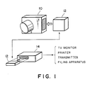
- Fig. 1 shows an arrangement of a solid-state camera system.
- a memory cartridge 12 as a solid-state memory apparatus for storing image information can be detached from a camera main body 10 of the solid-state camera.
- a reproducing apparatus 14 reproduces stored information in the memory cartridge 12.
- the memory cartridge 12 comprises, e.g., an IC memory device, a memory controller, and a backup power source therefor.
- an SRAM, a DRAM, an EPROM, an EEPROM, or the like is used.
- the memory cartridge 12 and the camera main body 10 are connected by using, e.g., a metal connector, a transmit coil, or a photocoupler.
- An image photographed by the camera main body 10 is stored in a predetermined format by the memory cartridge 12.
- the memory cartridge 12 By connecting the memory cartridge 12 to the reproducing apparatus 14 to reproduce the stored image, electronic image data can be transmitted from the reproducing apparatus to a TV monitor, a printer, a transmitter, a filing apparatus, and the like.
- the memory cartridge 12 since the memory cartridge 12 can be detached from the camera main body 10, communication between the memory cartridge 12 and the camera main body 10 must be perfect upon photographing. In addition, the memory cartridge 12 itself must eliminate a circuit defect, an insufficient capacity of the backup power source, or the like. If a user operates a release button without noticing these defects, he or she fails photographing because an image to be photographed is not recorded.
- the camera main body 10 must include a power source for driving various signal processors and exposure control means such as a lens driving means and an aperture driving means.
- a user therefore, must perform a maintenance operation for, e.g., checking the voltage of a power source battery of the camera main body 10 or replacing the battery before he or she uses the camera, resulting in a very cumbersome operation for a user.
- a maintenance operation for, e.g., checking the voltage of a power source battery of the camera main body 10 or replacing the battery before he or she uses the camera, resulting in a very cumbersome operation for a user.
- a write speed (or time) of the IC memory device in the memory cartridge 12 largely changes in accordance with the type of device. Therefore, as the memory capacity is increased, a difference between write times is increased.
- the size, connecting pins, and the like of the solid-state memory apparatus such as the memory cartridge 12 must be standardized.
- a solid-state camera comprises loading detecting means for detecting loading of detachable image storing means, checking means for checking a detection output from the loading detecting means and the loaded image storing means, and control means for performing control of each section which includes predetermined display control in accordance with a check result of the check means.
- the above solid-state camera can automatically detect whether the image storing means can be used. Therefore, in accordance with a detection result, necessary warning or any other display is performed, and control such as photographing prohibition is performed, thereby improving operability and a feel of use.
- a solid-state camera is an apparatus for recording information in a detachable solid-state memory apparatus, comprising detecting means for detecting specification information of a loaded solid-state memory apparatus, wherein an access timing of the solid-state memory apparatus is controlled in accordance with detection information of the detecting means.
- the solid-state camera Upon recording, the solid-state camera performs transfer to the solid-state memory apparatus at an access timing corresponding to a memory device of the solid-state memory apparatus. As a result, a solid-state memory apparatus using various memory devices can be utilized.
- a solid-state memory apparatus comprises characteristic code holding means for holding a characteristic code representing characteristics of an internal circuit, and reading means for reading the characteristic code held in the characteristic code holding means.
- the above solid-state memory apparatus can recognize the new device in accordance with the characteristic code and smoothly perform a corresponding operation.
- the internal circuit can be easily expanded or changed. Therefore, as long as the camera can recognize internal progress of a device even if the outer dimensions of the device are kept unchanged, the most advanced device can always be optimally used as a memory pack.
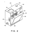
- Fig. 2 is a perspective view showing an outer appearance of an embodiment according to the present invention
- Fig. 3A is a sectional view showing a state in which an insertion portion for a memory cartridge as a solid-state memory apparatus is open
- Fig. 3B is a sectional view showing a state in which the memory cartridge is inserted in the insertion portion and the insertion portion is closed.
- a camera main body 20 comprises a cover 22, a cartridge holder 24 which can pivot about a pivot center 24a, a loading detection switch 26, electric contacts 28 for communicating with the memory cartridge, a release button 30, a liquid crystal display (LCD) device 32, a cover member 34, a cover biasing compression coil 36, a memory cartridge 38, memory contacts 38a of the memory cartridge 38, an eject button 40 for the memory cartridge 38, and a power switch 42 of the camera main body 20.
- LCD liquid crystal display
- the eject button 40 is operated to set the open state shown in Fig. 3A, and the memory cartridge 38 is inserted in the holder 24 in a direction indicated by an arrow shown in Fig. 3A. If a barrier shutter for protecting a contact is provided for the memory cartridge 38, the barrier shutter is opened by opening means (not shown) during insertion. When the memory cartridge 38 reaches a predetermined position deep in the holder 24, the cartridge 38 is locked by a locking mechanism (not shown). Thereafter, by closing the cover 22, the memory contacts 38a are brought into contact with and electrically connected to the electric contacts 28 of the camera body 20, as shown in Fig. 3B. After insertion is completed, the loading detection switch 26 is operated, and the state shown in Fig. 3B is held by a cover locking mechanism (not shown).
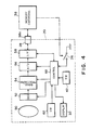
- Fig. 4 is a block diagram showing an arrangement of electric circuits of this embodiment.
- the same reference numerals as in Figs. 2, 3A, and 3B denote the same parts.
- the camera main body 20 includes a photographic lens 50, a CCD image pickup device 52, a signal processor 54, an A/D converter 56, an interface circuit 58 with respect to the memory cartridge 38, a controller 60 constituted by a microcomputer for controlling the overall system, and a switch 62 for inputting various commands.
- the image pickup device 52 converts an optical image of an object photographed by the photographic lens 50 into an electrical signal, and the signal processor 54 perform predetermined image signal processing.
- the A/D converter 56 digitizes an output from the signal processor 54. An output from the A/D converter 56 is supplied to and stored in the memory cartridge 38 via the interface circuit 58 and the contacts 28 and 38a.
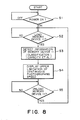
- Fig. 5 shows a control operation flow chart for performing checking in the above solid-state camera.
- the controller 60 checks an open/close state of the loading detection switch 26 (S2). If unloading is detected, the controller 60 performs warning by the display device 32 and/or a sound so as to cause the user to load the memory cartridge 38 (S4). If the memory cartridge 38 is already loaded, the controller 60 reads out various pieces of specification information stored beforehand in the loaded memory cartridge 38 (S5 and S6) and displays the readout information on the display device 32 (S7).
- Fig. 6 shows the format of communication data from the memory circuit 38 to the camera main body 20.
- the controller 60 displays a warning indicating that photographing cannot be performed on the display device 32 (S9), and prohibits photographing (S10). If a necessary memory capacity is remained, the controller 60 reads a remaining backup battery capacity of the memory cartridge 38 (S11). If the battery capacity is below a predetermined value, the controller 60 displays that photographing cannot be performed on the display device 32 and prohibits photographing (S9 and S10). If the battery capacity is over the predetermined value, the controller 60 displays that photographing can be performed (S13), waits for release (S14), and performs photographing/recording (i.e., writes an output from the image pickup device 52 in the memory cartridge 38) (S15). After recording (S15), the controller 60 updates information concerning the number of photographed frames, the memory remaining capacity, and the like (S16). The flow then returns to step S6, and the controller 60 checks the memory capacity and the backup battery capacity and waits for the next release.
- the flow may be modified such that a communication with the memory cartridge 38 is directly performed without checking the open/close state of the loading detection switch 26 immediately after the power source is switched on, and if the communication cannot be performed, unloading or defective loading of the memory cartridge is warned to prohibit photographing.
- the switch 26 is separately provided to detect loading completion of the memory cartridge 38.
- Some of the electric contacts 28 of the camera main body 20, however, may be used to detect loading. In this case, two contacts 28a of a plurality of electric contacts 28 are used for loading detection, and remaining contacts 28b are used for communication. One of the contacts 28 for loading detection is to be grounded.
- the memory contacts 38a are electrically connected to the contacts 28. In accordance with whether an electrical signal (voltage value or current value) from the contact 28a is lower or higher than a predetermined level, the controller 60 of the camera main body 20 checks whether loading is completed.
- all the electric contacts 28 can be used for both loading detection and communication in such a manner that loading detection and data communication are performed at different timings. In this manner, the number of contacts 28 and 38a can be reduced.
- a solid-state camera according to another embodiment of the present invention will be described below with reference to Figs. 7 to 9.
- Fig. 7 is a block diagram showing an arrangement of the embodiment in which the present invention is applied to a solid-state camera using a solid-state memory apparatus similar to the memory cartridge 38 of the above embodiment as a still image recording medium.
- a solid-state memory apparatus 65 comprising various IC memory devices and a CPU as a controller for controlling the IC memory devices can be detached from a camera main body 64.
- the solid-state memory apparatus 65 exchanges various information with the camera main body 64 via a predetermined bus line.
- the camera main body 64 comprises a photographic lens 66, a shutter 67, a solid-state image pickup device 68 such as a CCD, a signal processor 69, an A/D converter 70, a driver 71 for the image pickup device 68, a CPU 72 for controlling the overall system, a timing controller 73 for defining operation timings of the processor 69, the converter 70, and the driver 71 of the image pickup device 68, and a display/switch unit 74 including various switches and a display device.
- Fig. 7 An operation of Fig. 7 will be described below with reference to a flow chart shown in Fig. 8.
- S1 When a power switch of the camera main body 64 is turned on (S1), loading of the solid-state memory apparatus 65 is waited (S2).
- the CPU 72 communicates with the loaded solid-state memory apparatus 65 and detects specification information (e.g., memory device classification, a transfer speed upper limit, and a remaining capacity shown in Fig. 6) of the solid-state memory apparatus 65 (S3). On the basis of this information, the CPU 72 determines operation speeds of the device 68, the processor 69, the converter 70, and the driver 71 and controls the timing controller 73.
- specification information e.g., memory device classification, a transfer speed upper limit, and a remaining capacity shown in Fig. 6
- the CPU 72 Since a maximum continuous photographing speed is determined on the basis of the memory information obtained in step S3, the CPU 72 displays a possible maximum continuous photographing speed (S4), and monitors unloading of the solid-state memory apparatus 65 (S5).
- Fig. 9 is a block diagram showing an arrangement of still another embodiment of the present invention.
- the same reference numerals as in Fig. 7 denote the same parts.
- image data digitized by an A/D converter 70 is temporarily stored in a frame memory 75.
- the image data temporarily stored in the frame memory 75 is read out from the frame memory 75 at a speed corresponding to a transfer speed of a memory device of a solid-state memory 75 and written in the solid-state memory apparatus 65.
- the above embodiment employs an arrangement in which when the solid-state memory 65 is loaded, the CPU 72 of the camera main body 64 inquires classification of a memory device used as the solid-state memory apparatus 65.
- the arrangement may be made such that the above various types of information are mechanically set in the solid-state memory apparatus 65 and detecting means for detecting the mechanically set information may be provided for the camera main body 64. With this arrangement, the CPU need not communicate with the memory.
- the maximum continuous photographing speed of the solid-state camera is limited to a write enable speed of the solid-state memory apparatus 65 and displayed. Therefore, operability of the solid-state camera, especially its continuous photographing operability is improved.
- the solid-state camera has been exemplified.
- the present invention can be generally applied to an apparatus for recording a certain kind of information in a detachable solid-state memory apparatus.
- solid-state memory apparatus is obtained by applying the present invention to the memory cartridge and the solid-state memory apparatus of the above embodiments.
- Fig. 10 is a block diagram showing an arrangement of the embodiment of the present invention.
- a solid-state memory apparatus 65 includes a status output line 76, an address/control input line 77, a clock input line 78, and a data input/output line 79.
- the data input/output line 79 is constituted by one signal line.
- the data input/output line is constituted by signal lines in the number corresponding to the number of parallel signals.
- the solid-state memory apparatus 65 also includes a memory device 80, an address counter 81, an address preset circuit 82, a controller 83, a recognition code storing circuit 84, and a buffer 85.
- the input lines 77 and 78 and the input/output line 79 are connected to a solid-state camera via electric contacts as shown in Fig. 3.
- an operation mode of the solid-state memory apparatus 65 is set. That is, a clock signal is supplied to the clock input line 78 and a binary signal is supplied to the address/control input line 77 at timings shown in Fig. 11.
- Table 1 A relationship between binary values at portions A, B, C, and D in Fig. 11 and the operation modes is shown in Table 1 below. Note that a maximum of 16 commands can be used by using four bits in this embodiment. Table 1 A B C D Operation Mode 0 0 0 0 0 Counter Clear 0 0 0 1 Counter Up 0 0 1 0 Counter Down 0 0 1 1 Counter Down/Load (Followed by E to J) 0 1 0 0 0 Memory Clear 0 1 0 1 Memory Readout 0 1 1 0 Memory Write 0 1 1 1 Recognition Code Readout 1 X X X System Reservation
- the controller 83 decodes a command from the address/control input line 77 and operates the respective sections by the designated operation mode.
- image data can be randomly accessed by designating the number of a photograph. That is, when the number of photographs to be read is designated, the address preset circuit 82 loads its start address in the address counter 81, and the address counter 81 sequentially counts up. In this manner, write or read of a storage area corresponding to the designated number can be performed.
- a recognition code can be output from the recognition code storing circuit 84 to the camera main body. More specifically, when "0111" is supplied from the camera main body to the address/control input line 77, the controller 83 sends a command to the recognition code storing circuit 84 to output a stored recognition code. This recognition code is output to the camera main body via the output buffer 85 and the data input/output line 79. Note that the recognition code storing circuit 84 stores various types of specification information as shown in Fig. 6.
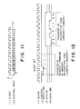
- Fig. 12 is a timing chart for explaining the above operation.
- a clock signal is normally supplied from the camera main body to the solid-state memory apparatus 65, and the internal circuit in the solid-state memory apparatus 65 operates in synchronism with this clock.
- a readout command "0111" of memory recognition code is supplied from the camera main body to the address/control input line 77 at the timing shown in Fig. 12. The first “0" is a start bit.
- the controller 83 interprets this command and sets a status bit at "H", thereby informing the camera main body that the data is effective.
- the controller 83 causes the recognition code storing circuit 84 to output storage data (in this embodiment, "00101100") to the data input/output line 79 via the buffer 85.
- a read-only memory or a combinational logic circuit, e.g., is used as the recognition code storing circuit 84.
- this recognition code may be determined to include information such as a memory capacity, a transfer rate, and an image size, its length is not limited to 8 bits.
- the recognition code is read out by a command response scheme.
- An exclusive readout terminal may be used to read out the code.
- data exchange is performed by four types of signal lines. Data exchange, however, may be performed by using a larger or smaller number of signal lines.
- a new electronic device can be used to achieve a large capacity and a high speed.
Abstract
Description
- The present invention relates to a solid-state camera using a solid-state memory apparatus as a recording medium for a photographed image and the solid-state memory apparatus.
- An electronic still camera using a memory not requiring a movable mechanism for recording/reproduction of information (to be referred to as a solid-state camera hereinafter) has attracted attention as a successor of a silver chloride still camera and a video floppy electronic still camera. In an electronic still camera, instantaneous reproduction of a photographed image, image transfer, computer image processing, electronic image filing and the like can be easily performed by electronically processing image information. In the case of using a compact magnetic sheet called a video floppy as a recording medium, however, movable portions such as a rotating mechanism for the magnetic sheet and a head moving mechanism for positioning a magnetic head with precision of several tens to hundreds of µm in terms of a track pitch are required, thereby increasing a manufacturing cost of a camera and limiting use environments and an operation speed. These problems are similarly posed when an optical disk or optical magnetic disk is used as a recording medium.
- The solid-state camera has been proposed as a camera capable of solving the above problems. Fig. 1 shows an arrangement of a solid-state camera system. Referring to Fig. 1, a
memory cartridge 12 as a solid-state memory apparatus for storing image information can be detached from a cameramain body 10 of the solid-state camera. A reproducingapparatus 14 reproduces stored information in thememory cartridge 12. Thememory cartridge 12 comprises, e.g., an IC memory device, a memory controller, and a backup power source therefor. As the IC memory device, an SRAM, a DRAM, an EPROM, an EEPROM, or the like is used. Thememory cartridge 12 and the cameramain body 10 are connected by using, e.g., a metal connector, a transmit coil, or a photocoupler. An image photographed by the cameramain body 10 is stored in a predetermined format by thememory cartridge 12. By connecting thememory cartridge 12 to the reproducingapparatus 14 to reproduce the stored image, electronic image data can be transmitted from the reproducing apparatus to a TV monitor, a printer, a transmitter, a filing apparatus, and the like. - In the conventional solid-state camera having the above arrangement, however, since the
memory cartridge 12 can be detached from the cameramain body 10, communication between thememory cartridge 12 and the cameramain body 10 must be perfect upon photographing. In addition, thememory cartridge 12 itself must eliminate a circuit defect, an insufficient capacity of the backup power source, or the like. If a user operates a release button without noticing these defects, he or she fails photographing because an image to be photographed is not recorded. - Furthermore, the camera
main body 10 must include a power source for driving various signal processors and exposure control means such as a lens driving means and an aperture driving means. A user, therefore, must perform a maintenance operation for, e.g., checking the voltage of a power source battery of the cameramain body 10 or replacing the battery before he or she uses the camera, resulting in a very cumbersome operation for a user. Even if the power source capacity of the cameramain body 10 is increased, not only this maintenance operation is not basically omitted, but also the size of the cameralmain body 10 is increased by the increase in capacity. - Moreover, a write speed (or time) of the IC memory device in the
memory cartridge 12 largely changes in accordance with the type of device. Therefore, as the memory capacity is increased, a difference between write times is increased. - If data transfer is not performed at a proper speed corresponding to the write speed, data write may be failed to lose data.
- In order to spread the solid-state camera and the solid-state memory apparatus as described above, the size, connecting pins, and the like of the solid-state memory apparatus such as the
memory cartridge 12 must be standardized. - If, however, techniques for realizing a large capacity, a high speed, and low power consumption of the IC memory device of the
memory cartridge 12 rapidly progress, standardization of the size may prevent use of advanced circuit devices. - It is an object of the present invention to solve the above problems.
- More specifically, it is an object of the present invention to provide a solid-state camera capable of automatically checking whether photographing can be performed and performing a necessary display or warning.
- It is another object of the present invention to provide a solid-state camera capable of automatically coping with different types of memory device of a solid-state memory apparatus.
- It is still another object of the present invention to provide a solid-state memory apparatus for use in the above solid-state camera, which does not prevent an increase in memory capacity even when its size is standardized.
- A solid-state camera according to an embodiment of the present invention comprises loading detecting means for detecting loading of detachable image storing means, checking means for checking a detection output from the loading detecting means and the loaded image storing means, and control means for performing control of each section which includes predetermined display control in accordance with a check result of the check means.
- The above solid-state camera can automatically detect whether the image storing means can be used. Therefore, in accordance with a detection result, necessary warning or any other display is performed, and control such as photographing prohibition is performed, thereby improving operability and a feel of use.
- A solid-state camera according to another embodiment of the present invention is an apparatus for recording information in a detachable solid-state memory apparatus, comprising detecting means for detecting specification information of a loaded solid-state memory apparatus, wherein an access timing of the solid-state memory apparatus is controlled in accordance with detection information of the detecting means.
- Upon recording, the solid-state camera performs transfer to the solid-state memory apparatus at an access timing corresponding to a memory device of the solid-state memory apparatus. As a result, a solid-state memory apparatus using various memory devices can be utilized.
- A solid-state memory apparatus according to still another embodiment of the present invention comprises characteristic code holding means for holding a characteristic code representing characteristics of an internal circuit, and reading means for reading the characteristic code held in the characteristic code holding means.
- Even when a new device is used as the internal circuit device to increase a memory capacity or a speed, the above solid-state memory apparatus can recognize the new device in accordance with the characteristic code and smoothly perform a corresponding operation. As a result, the internal circuit can be easily expanded or changed. Therefore, as long as the camera can recognize internal progress of a device even if the outer dimensions of the device are kept unchanged, the most advanced device can always be optimally used as a memory pack.
- The other objects and features of the present invention will become apparent from the following description and the accompanying drawings.
-
- Fig. 1 is a perspective view showing an arrangement of a conventional solid-state camera system;
- Fig. 2 is a perspective view showing an outer appearance of solid-state camera according to an embodiment of the present invention;
- Fig. 3A is a sectional view showing a state in which a cartridge insertion portion is open;
- Fig. 3B is a sectional view showing a state in which a cartridge is inserted;
- Fig. 4 is block diagram showing an electric circuit arrangement of the embodiment;
- Fig. 5 is a flow chart for explaining an operation of the embodiment;
- Fig. 6 is a schematic view showing a format of communication data;
- Fig. 7 is a block diagram showing an arrangement of another embodiment of the present invention;
- Fig. 8 is a flow chart for explaining the embodiment;
- Fig. 9 is a block diagram showing an arrangement of still another embodiment of the present invention;
- Fig. 10 is a block diagram showing an embodiment of a solid-state memory apparatus of the present invention;
- Fig. 11 is a timing chart of a command; and
- Fig. 12 is a timing chart upon a recognition code read operation.
- Embodiments of the present invention will be described below with reference to the accompanying drawings.
- Fig. 2 is a perspective view showing an outer appearance of an embodiment according to the present invention, Fig. 3A is a sectional view showing a state in which an insertion portion for a memory cartridge as a solid-state memory apparatus is open, and Fig. 3B is a sectional view showing a state in which the memory cartridge is inserted in the insertion portion and the insertion portion is closed. In these drawings, a camera
main body 20 comprises acover 22, acartridge holder 24 which can pivot about apivot center 24a, aloading detection switch 26,electric contacts 28 for communicating with the memory cartridge, arelease button 30, a liquid crystal display (LCD)device 32, acover member 34, a coverbiasing compression coil 36, amemory cartridge 38,memory contacts 38a of thememory cartridge 38, aneject button 40 for thememory cartridge 38, and apower switch 42 of the cameramain body 20. - An operation of each section will be described below. In order to perform photographing, the
eject button 40 is operated to set the open state shown in Fig. 3A, and thememory cartridge 38 is inserted in theholder 24 in a direction indicated by an arrow shown in Fig. 3A. If a barrier shutter for protecting a contact is provided for thememory cartridge 38, the barrier shutter is opened by opening means (not shown) during insertion. When thememory cartridge 38 reaches a predetermined position deep in theholder 24, thecartridge 38 is locked by a locking mechanism (not shown). Thereafter, by closing thecover 22, thememory contacts 38a are brought into contact with and electrically connected to theelectric contacts 28 of thecamera body 20, as shown in Fig. 3B. After insertion is completed, theloading detection switch 26 is operated, and the state shown in Fig. 3B is held by a cover locking mechanism (not shown). - Fig. 4 is a block diagram showing an arrangement of electric circuits of this embodiment. In Fig. 4, the same reference numerals as in Figs. 2, 3A, and 3B denote the same parts. Referring to Fig. 4, the camera
main body 20 includes aphotographic lens 50, a CCDimage pickup device 52, asignal processor 54, an A/D converter 56, aninterface circuit 58 with respect to thememory cartridge 38, acontroller 60 constituted by a microcomputer for controlling the overall system, and aswitch 62 for inputting various commands. - The
image pickup device 52 converts an optical image of an object photographed by thephotographic lens 50 into an electrical signal, and thesignal processor 54 perform predetermined image signal processing. The A/D converter 56 digitizes an output from thesignal processor 54. An output from the A/D converter 56 is supplied to and stored in thememory cartridge 38 via theinterface circuit 58 and thecontacts - Fig. 5 shows a control operation flow chart for performing checking in the above solid-state camera. Referring to Fig. 5, when a power source is switched on by the power switch 42 (S1), the
controller 60 checks an open/close state of the loading detection switch 26 (S2). If unloading is detected, thecontroller 60 performs warning by thedisplay device 32 and/or a sound so as to cause the user to load the memory cartridge 38 (S4). If thememory cartridge 38 is already loaded, thecontroller 60 reads out various pieces of specification information stored beforehand in the loaded memory cartridge 38 (S5 and S6) and displays the readout information on the display device 32 (S7). Fig. 6 shows the format of communication data from thememory circuit 38 to the cameramain body 20. - If the memory capacity is not remained, the
controller 60 displays a warning indicating that photographing cannot be performed on the display device 32 (S9), and prohibits photographing (S10). If a necessary memory capacity is remained, thecontroller 60 reads a remaining backup battery capacity of the memory cartridge 38 (S11). If the battery capacity is below a predetermined value, thecontroller 60 displays that photographing cannot be performed on thedisplay device 32 and prohibits photographing (S9 and S10). If the battery capacity is over the predetermined value, thecontroller 60 displays that photographing can be performed (S13), waits for release (S14), and performs photographing/recording (i.e., writes an output from theimage pickup device 52 in the memory cartridge 38) (S15). After recording (S15), thecontroller 60 updates information concerning the number of photographed frames, the memory remaining capacity, and the like (S16). The flow then returns to step S6, and thecontroller 60 checks the memory capacity and the backup battery capacity and waits for the next release. - The flow may be modified such that a communication with the
memory cartridge 38 is directly performed without checking the open/close state of theloading detection switch 26 immediately after the power source is switched on, and if the communication cannot be performed, unloading or defective loading of the memory cartridge is warned to prohibit photographing. - In the above embodiment, the
switch 26 is separately provided to detect loading completion of thememory cartridge 38. Some of theelectric contacts 28 of the cameramain body 20, however, may be used to detect loading. In this case, twocontacts 28a of a plurality ofelectric contacts 28 are used for loading detection, and remainingcontacts 28b are used for communication. One of thecontacts 28 for loading detection is to be grounded. When loading of thememory cartridge 38 is completed, thememory contacts 38a are electrically connected to thecontacts 28. In accordance with whether an electrical signal (voltage value or current value) from thecontact 28a is lower or higher than a predetermined level, thecontroller 60 of the cameramain body 20 checks whether loading is completed. - It is a matter of course that all the
electric contacts 28 can be used for both loading detection and communication in such a manner that loading detection and data communication are performed at different timings. In this manner, the number ofcontacts - As is apparent from the above description, according to this embodiment, whether an image to be photographed can be recorded in the memory cartridge is automatically checked. Therefore, photographing can be performed more reliably and more rapidly.
- A solid-state camera according to another embodiment of the present invention will be described below with reference to Figs. 7 to 9.
- Fig. 7 is a block diagram showing an arrangement of the embodiment in which the present invention is applied to a solid-state camera using a solid-state memory apparatus similar to the
memory cartridge 38 of the above embodiment as a still image recording medium. Referring to Fig. 7, a solid-state memory apparatus 65 comprising various IC memory devices and a CPU as a controller for controlling the IC memory devices can be detached from a cameramain body 64. The solid-state memory apparatus 65 exchanges various information with the cameramain body 64 via a predetermined bus line. The cameramain body 64 comprises aphotographic lens 66, ashutter 67, a solid-stateimage pickup device 68 such as a CCD, asignal processor 69, an A/D converter 70, adriver 71 for theimage pickup device 68, aCPU 72 for controlling the overall system, atiming controller 73 for defining operation timings of theprocessor 69, theconverter 70, and thedriver 71 of theimage pickup device 68, and a display/switch unit 74 including various switches and a display device. - An operation of Fig. 7 will be described below with reference to a flow chart shown in Fig. 8. When a power switch of the camera
main body 64 is turned on (S1), loading of the solid-state memory apparatus 65 is waited (S2). TheCPU 72 communicates with the loaded solid-state memory apparatus 65 and detects specification information (e.g., memory device classification, a transfer speed upper limit, and a remaining capacity shown in Fig. 6) of the solid-state memory apparatus 65 (S3). On the basis of this information, theCPU 72 determines operation speeds of thedevice 68, theprocessor 69, theconverter 70, and thedriver 71 and controls thetiming controller 73. - When a user depresses a shutter switch of the display/
switch unit 74, theshutter 67 is opened, and an output from theimage pickup device 68 is transferred to and written in the solid-state memory apparatus 65 at the above timings via thesignal processor 69 and the A/D converter 70. - Since a maximum continuous photographing speed is determined on the basis of the memory information obtained in step S3, the
CPU 72 displays a possible maximum continuous photographing speed (S4), and monitors unloading of the solid-state memory apparatus 65 (S5). - Fig. 9 is a block diagram showing an arrangement of still another embodiment of the present invention. In Fig. 9, the same reference numerals as in Fig. 7 denote the same parts.
- In this embodiment, image data digitized by an A/
D converter 70 is temporarily stored in aframe memory 75. The image data temporarily stored in theframe memory 75 is read out from theframe memory 75 at a speed corresponding to a transfer speed of a memory device of a solid-state memory 75 and written in the solid-state memory apparatus 65. - The above embodiment employs an arrangement in which when the solid-
state memory 65 is loaded, theCPU 72 of the cameramain body 64 inquires classification of a memory device used as the solid-state memory apparatus 65. The arrangement, however, may be made such that the above various types of information are mechanically set in the solid-state memory apparatus 65 and detecting means for detecting the mechanically set information may be provided for the cameramain body 64. With this arrangement, the CPU need not communicate with the memory. - In this embodiment, the maximum continuous photographing speed of the solid-state camera is limited to a write enable speed of the solid-
state memory apparatus 65 and displayed. Therefore, operability of the solid-state camera, especially its continuous photographing operability is improved. - In the above description, the solid-state camera has been exemplified. The present invention, however, can be generally applied to an apparatus for recording a certain kind of information in a detachable solid-state memory apparatus.
- As is apparent from the above description, according to this embodiment, information can be reliably recorded even when solid-state memory apparatuses using various types of memory devices are replaced and used.
- An embodiment of a solid-state memory apparatus according to the present invention will be described below with reference to Figs. 10 to 12.
- Note that the solid-state memory apparatus according to this embodiment is obtained by applying the present invention to the memory cartridge and the solid-state memory apparatus of the above embodiments.
- Fig. 10 is a block diagram showing an arrangement of the embodiment of the present invention. Referring to Fig. 10, a solid-
state memory apparatus 65 according to this embodiment includes astatus output line 76, an address/control input line 77, aclock input line 78, and a data input/output line 79. In the case of a serial signal, the data input/output line 79 is constituted by one signal line. In the case of a parallel signal, however, the data input/output line is constituted by signal lines in the number corresponding to the number of parallel signals. The solid-state memory apparatus 65 also includes amemory device 80, anaddress counter 81, an addresspreset circuit 82, acontroller 83, a recognitioncode storing circuit 84, and abuffer 85. - The input lines 77 and 78 and the input/
output line 79 are connected to a solid-state camera via electric contacts as shown in Fig. 3. - When the camera sends a predetermined command to the address/
control input line 77, an operation mode of the solid-state memory apparatus 65 is set. That is, a clock signal is supplied to theclock input line 78 and a binary signal is supplied to the address/control input line 77 at timings shown in Fig. 11. - A relationship between binary values at portions A, B, C, and D in Fig. 11 and the operation modes is shown in Table 1 below. Note that a maximum of 16 commands can be used by using four bits in this embodiment.
Table 1 A B C D Operation Mode 0 0 0 0 Counter Clear 0 0 0 1 Counter Up 0 0 1 0 Counter Down 0 0 1 1 Counter Down/Load (Followed by E to J) 0 1 0 0 Memory Clear 0 1 0 1 Memory Readout 0 1 1 0 Memory Write 0 1 1 1 Recognition Code Readout 1 X X X System Reservation - In synchronism with a clock supplied from the
clock input line 78, thecontroller 83 decodes a command from the address/control input line 77 and operates the respective sections by the designated operation mode. - For example, in this embodiment, by storing memory addresses corresponding to the number of photographs in the address preset
circuit 82, image data can be randomly accessed by designating the number of a photograph. That is, when the number of photographs to be read is designated, the address presetcircuit 82 loads its start address in theaddress counter 81, and the address counter 81 sequentially counts up. In this manner, write or read of a storage area corresponding to the designated number can be performed. - Similarly, a recognition code can be output from the recognition
code storing circuit 84 to the camera main body. More specifically, when "0111" is supplied from the camera main body to the address/control input line 77, thecontroller 83 sends a command to the recognitioncode storing circuit 84 to output a stored recognition code. This recognition code is output to the camera main body via theoutput buffer 85 and the data input/output line 79. Note that the recognitioncode storing circuit 84 stores various types of specification information as shown in Fig. 6. - Fig. 12 is a timing chart for explaining the above operation.
- A clock signal is normally supplied from the camera main body to the solid-
state memory apparatus 65, and the internal circuit in the solid-state memory apparatus 65 operates in synchronism with this clock. A readout command "0111" of memory recognition code is supplied from the camera main body to the address/control input line 77 at the timing shown in Fig. 12. The first "0" is a start bit. Thecontroller 83 interprets this command and sets a status bit at "H", thereby informing the camera main body that the data is effective. In synchronism with a clock, thecontroller 83 causes the recognitioncode storing circuit 84 to output storage data (in this embodiment, "00101100") to the data input/output line 79 via thebuffer 85. A read-only memory or a combinational logic circuit, e.g., is used as the recognitioncode storing circuit 84. - When this recognition code may be determined to include information such as a memory capacity, a transfer rate, and an image size, its length is not limited to 8 bits.
- In the above embodiment, the recognition code is read out by a command response scheme. An exclusive readout terminal, however, may be used to read out the code. In addition, in the above embodiment, data exchange is performed by four types of signal lines. Data exchange, however, may be performed by using a larger or smaller number of signal lines.
- As is easily understood from the above description, according to the embodiments of the present invention, regardless of an outer shape or standardization of an interface, a new electronic device can be used to achieve a large capacity and a high speed.
Claims (46)
loading detecting means for detecting loading of detachable image storing means;
checking means for checking a detection output from said loading detecting means and said loaded image storing means; and
control means for performing control of each section which includes predetermined display control in accordance with a check result of said detecting means.
wherein an access timing of said image storing means is controlled in accordance with detection information of said detecting means.
detecting means for detecting specification information of said loaded image storing means; and
storing means for temporarily storing information to be recorded in said image storing means,
wherein a readout timing of information from said image storing means is controlled in accordance with detection information from said detecting means.
wherein a maximum continuous photographing speed is set in accordance with detection information from said detecting means.
characteristic code holding means for holding a characteristic code representing characteristics of an internal circuit; and
readout means for reading out the characteristic code of said characteristic code holding means.
Applications Claiming Priority (6)
| Application Number | Priority Date | Filing Date | Title |
|---|---|---|---|
| JP269558/88 | 1988-10-27 | ||
| JP63269558A JPH02118990A (en) | 1988-10-27 | 1988-10-27 | Solid-state memory device |
| JP1039343A JP2712489B2 (en) | 1989-02-21 | 1989-02-21 | Solid camera |
| JP39343/89 | 1989-02-21 | ||
| JP1079587A JPH02257341A (en) | 1989-03-30 | 1989-03-30 | Information recording device |
| JP79587/89 | 1989-03-30 |
Publications (2)
| Publication Number | Publication Date |
|---|---|
| EP0366474A1 true EP0366474A1 (en) | 1990-05-02 |
| EP0366474B1 EP0366474B1 (en) | 1994-12-28 |
Family
ID=27290108
Family Applications (1)
| Application Number | Title | Priority Date | Filing Date |
|---|---|---|---|
| EP89311078A Expired - Lifetime EP0366474B1 (en) | 1988-10-27 | 1989-10-26 | Solid-state camera and solid-state memory apparatus |
Country Status (3)
| Country | Link |
|---|---|
| US (1) | US6118929A (en) |
| EP (1) | EP0366474B1 (en) |
| DE (1) | DE68920273T2 (en) |
Cited By (5)
| Publication number | Priority date | Publication date | Assignee | Title |
|---|---|---|---|---|
| EP0528280A1 (en) * | 1991-08-09 | 1993-02-24 | Kabushiki Kaisha Toshiba | Memory card apparatus |
| US5262868A (en) * | 1991-01-14 | 1993-11-16 | Fuji Photo Film Co., Ltd. | Digital electronic still camera with function alarming low voltage of built-in battery of memory card |
| EP0585825A1 (en) * | 1992-08-31 | 1994-03-09 | Canon Kabushiki Kaisha | Electronic apparatus |
| GB2312352A (en) * | 1996-04-15 | 1997-10-22 | Euroquest Solutions Ltd | Video imaging system |
| EP0945009A1 (en) * | 1996-12-13 | 1999-09-29 | Disposable Video Camcorders Limited | Video recording apparatus |
Families Citing this family (14)
| Publication number | Priority date | Publication date | Assignee | Title |
|---|---|---|---|---|
| US6738090B2 (en) * | 1997-10-23 | 2004-05-18 | Eastman Kodak Company | System and method for using a single intelligence circuit for a plurality of imaging rendering components |
| US6587140B2 (en) * | 1997-10-23 | 2003-07-01 | Eastman Kodak Company | System and method for using a single intelligence circuit in both a digital camera and printer |
| JPH11331764A (en) * | 1998-03-20 | 1999-11-30 | Sony Corp | Recording and reproducing device and its method |
| JP2002209132A (en) * | 2001-01-12 | 2002-07-26 | Minolta Co Ltd | Digital camera |
| US6930727B2 (en) * | 2001-03-30 | 2005-08-16 | Sony Corporation | Protection-cover opening/closing mechanism for recording/playback apparatus |
| US7765334B2 (en) * | 2004-05-12 | 2010-07-27 | Canon Kabushiki Kaisha | Electronic apparatus for use with removable storage medium, control method therefor, and program for implementing the method |
| US20070076325A1 (en) * | 2005-09-20 | 2007-04-05 | Nokia Corporation | Apparatus for indicating a state of a device |
| KR101467928B1 (en) * | 2007-07-23 | 2014-12-04 | 삼성전자주식회사 | A/v apparatus for displaying its information and method thereof |
| US8199251B2 (en) * | 2008-07-07 | 2012-06-12 | Woodman Labs, Inc. | Camera housing with integrated expansion module |
| DE202019107267U1 (en) | 2018-08-07 | 2020-02-27 | Gopro, Inc. | Camera and camera holder |
| USD905786S1 (en) | 2018-08-31 | 2020-12-22 | Gopro, Inc. | Camera mount |
| USD894256S1 (en) | 2018-08-31 | 2020-08-25 | Gopro, Inc. | Camera mount |
| USD920419S1 (en) | 2019-09-17 | 2021-05-25 | Gopro, Inc. | Camera |
| USD946074S1 (en) | 2020-08-14 | 2022-03-15 | Gopro, Inc. | Camera |
Citations (2)
| Publication number | Priority date | Publication date | Assignee | Title |
|---|---|---|---|---|
| DE3235735A1 (en) * | 1981-09-28 | 1983-04-07 | Staar S.A., 1080 Bruxelles | ELECTRONIC IMAGE CAMERA WITH DISCRETE, WRITABLE PRESENT STORAGE UNITS |
| US4837628A (en) * | 1986-07-14 | 1989-06-06 | Kabushiki Kaisha Toshiba | Electronic still camera for recording still picture on memory card with mode selecting shutter release |
Family Cites Families (21)
| Publication number | Priority date | Publication date | Assignee | Title |
|---|---|---|---|---|
| JPS564992A (en) * | 1979-06-26 | 1981-01-19 | Olympus Optical Co Ltd | Recording and reproducing device |
| US4420773A (en) * | 1980-06-30 | 1983-12-13 | Nippon Kogaku K.K. | Electronic photographic camera |
| JPS5714261A (en) * | 1980-06-30 | 1982-01-25 | Nippon Kogaku Kk <Nikon> | Charge storage time controller for solidstate image sensor |
| JPS5792981A (en) * | 1980-11-29 | 1982-06-09 | Nippon Kogaku Kk <Nikon> | Electronic camera system |
| JPS58155586A (en) * | 1982-03-10 | 1983-09-16 | Olympus Optical Co Ltd | Disc pack for electrostatic photographic device |
| US4651227A (en) * | 1982-08-20 | 1987-03-17 | Olympus Optical Co., Ltd. | Video signal recording apparatus with A/D conversion |
| JPS6230484A (en) * | 1985-08-01 | 1987-02-09 | Nippon Kogaku Kk <Nikon> | Electronic still camera |
| JPS62254249A (en) * | 1986-04-28 | 1987-11-06 | Toshiba Corp | Reading system for card memory capacity |
| JP2538564B2 (en) * | 1986-05-21 | 1996-09-25 | キヤノン株式会社 | Recording device |
| JPH0654596B2 (en) * | 1986-08-08 | 1994-07-20 | キヤノン株式会社 | Electronic camera |
| JPS63100696A (en) * | 1986-10-16 | 1988-05-02 | Fujitsu Ltd | Magnetic bubble memory cassette device |
| KR910006609B1 (en) * | 1986-12-18 | 1991-08-29 | 가시오 게이상기 가부시기가이샤 | Electronic still camera |
| JPS63161787A (en) * | 1986-12-24 | 1988-07-05 | Kyocera Corp | Electronic still camera |
| JPS63163588A (en) * | 1986-12-25 | 1988-07-07 | Toshiba Corp | Ic card |
| JPS63241761A (en) * | 1987-03-30 | 1988-10-07 | Hitachi Ltd | Still picture recording and reproducing device |
| US4907231A (en) * | 1987-05-06 | 1990-03-06 | Fuji Photo Film Co., Ltd. | Memory cartridge-connectable electronic device such as electronic still video camera |
| JPS63284988A (en) * | 1987-05-18 | 1988-11-22 | Toshiba Corp | Digital electronic camera |
| JPH0620283B2 (en) * | 1987-05-19 | 1994-03-16 | 富士写真フイルム株式会社 | Image data recording device |
| US4887161A (en) * | 1987-05-28 | 1989-12-12 | Fuji Photo Film Co., Ltd. | Memory cartridge and digital electronic still video camera in which said memory cartridge is freely loadable/unloadable |
| US4827347A (en) * | 1988-08-22 | 1989-05-02 | Eastman Kodak Company | Electronic camera with proofing feature |
| JP2712497B2 (en) * | 1989-03-02 | 1998-02-10 | キヤノン株式会社 | Solid camera |
-
1989
- 1989-10-26 EP EP89311078A patent/EP0366474B1/en not_active Expired - Lifetime
- 1989-10-26 DE DE68920273T patent/DE68920273T2/en not_active Expired - Fee Related
-
1995
- 1995-04-27 US US08/430,157 patent/US6118929A/en not_active Expired - Lifetime
Patent Citations (2)
| Publication number | Priority date | Publication date | Assignee | Title |
|---|---|---|---|---|
| DE3235735A1 (en) * | 1981-09-28 | 1983-04-07 | Staar S.A., 1080 Bruxelles | ELECTRONIC IMAGE CAMERA WITH DISCRETE, WRITABLE PRESENT STORAGE UNITS |
| US4837628A (en) * | 1986-07-14 | 1989-06-06 | Kabushiki Kaisha Toshiba | Electronic still camera for recording still picture on memory card with mode selecting shutter release |
Cited By (8)
| Publication number | Priority date | Publication date | Assignee | Title |
|---|---|---|---|---|
| US5262868A (en) * | 1991-01-14 | 1993-11-16 | Fuji Photo Film Co., Ltd. | Digital electronic still camera with function alarming low voltage of built-in battery of memory card |
| EP0528280A1 (en) * | 1991-08-09 | 1993-02-24 | Kabushiki Kaisha Toshiba | Memory card apparatus |
| US5579502A (en) * | 1991-08-09 | 1996-11-26 | Kabushiki Kaisha Toshiba | Memory card apparatus using EEPROMS for storing data and an interface buffer for buffering data transfer between the EEPROMS and an external device |
| EP0585825A1 (en) * | 1992-08-31 | 1994-03-09 | Canon Kabushiki Kaisha | Electronic apparatus |
| GB2312352A (en) * | 1996-04-15 | 1997-10-22 | Euroquest Solutions Ltd | Video imaging system |
| EP0945009A1 (en) * | 1996-12-13 | 1999-09-29 | Disposable Video Camcorders Limited | Video recording apparatus |
| EP0945009A4 (en) * | 1996-12-13 | 2002-05-02 | Disposable Video Camcorders Lt | Video recording apparatus |
| US6957011B2 (en) | 1996-12-13 | 2005-10-18 | Disposable Video Camcorders Limited | Video recording apparatus |
Also Published As
| Publication number | Publication date |
|---|---|
| EP0366474B1 (en) | 1994-12-28 |
| US6118929A (en) | 2000-09-12 |
| DE68920273D1 (en) | 1995-02-09 |
| DE68920273T2 (en) | 1995-05-11 |
Similar Documents
| Publication | Publication Date | Title |
|---|---|---|
| EP0366474A1 (en) | Solid-state camera and solid-state memory apparatus | |
| US5627587A (en) | Solid-state camera in which a removable solid state memory having a backup battery is used as an image recording device | |
| US5091787A (en) | Memory cartridge-connectable electronic device such as electronic still video camera | |
| EP0372514A2 (en) | Memory apparatus and handling apparatus therefor | |
| US5159458A (en) | Camera sensing when a memory cartridge is installed | |
| US5854875A (en) | Information recording appartus connectable to plural types of information recording media for recording information | |
| US5821996A (en) | Solid-sate camera with solid-state memory for holding characteristic code representing characteristic of an internal circuit | |
| JPH053073B2 (en) | ||
| JPH04207488A (en) | Electronic still camera with spare memory | |
| JP2712489B2 (en) | Solid camera | |
| JPH10145717A (en) | Electronic camera | |
| US6344873B1 (en) | Film reading apparatus and method | |
| JP3528058B2 (en) | Digital still camera | |
| JPH01258091A (en) | Memory card | |
| JP2767257B2 (en) | Solid camera | |
| JP3143517B2 (en) | Recording device | |
| JP2859267B2 (en) | Still image recording device | |
| JP2759660B2 (en) | Solid camera | |
| JPS6320590A (en) | Memory card | |
| JP3532614B2 (en) | Memory packs and electronics | |
| JPH02257341A (en) | Information recording device | |
| JPH04165771A (en) | Electronic camera | |
| JP3140607B2 (en) | Information reading device | |
| JP2005026807A (en) | Moving picture recording apparatus having loading slots for a plurality of recording media | |
| JPH04363978A (en) | Camera |
Legal Events
| Date | Code | Title | Description |
|---|---|---|---|
| PUAI | Public reference made under article 153(3) epc to a published international application that has entered the european phase |
Free format text: ORIGINAL CODE: 0009012 |
|
| AK | Designated contracting states |
Kind code of ref document: A1 Designated state(s): DE FR GB |
|
| 17P | Request for examination filed |
Effective date: 19900918 |
|
| 17Q | First examination report despatched |
Effective date: 19920811 |
|
| GRAA | (expected) grant |
Free format text: ORIGINAL CODE: 0009210 |
|
| AK | Designated contracting states |
Kind code of ref document: B1 Designated state(s): DE FR GB |
|
| REF | Corresponds to: |
Ref document number: 68920273 Country of ref document: DE Date of ref document: 19950209 |
|
| ET | Fr: translation filed | ||
| PLBE | No opposition filed within time limit |
Free format text: ORIGINAL CODE: 0009261 |
|
| STAA | Information on the status of an ep patent application or granted ep patent |
Free format text: STATUS: NO OPPOSITION FILED WITHIN TIME LIMIT |
|
| 26N | No opposition filed | ||
| REG | Reference to a national code |
Ref country code: GB Ref legal event code: IF02 |
|
| PGFP | Annual fee paid to national office [announced via postgrant information from national office to epo] |
Ref country code: DE Payment date: 20071031 Year of fee payment: 19 |
|
| PGFP | Annual fee paid to national office [announced via postgrant information from national office to epo] |
Ref country code: FR Payment date: 20071022 Year of fee payment: 19 Ref country code: GB Payment date: 20071005 Year of fee payment: 19 |
|
| GBPC | Gb: european patent ceased through non-payment of renewal fee |
Effective date: 20081026 |
|
| REG | Reference to a national code |
Ref country code: FR Ref legal event code: ST Effective date: 20090630 |
|
| PG25 | Lapsed in a contracting state [announced via postgrant information from national office to epo] |
Ref country code: DE Free format text: LAPSE BECAUSE OF NON-PAYMENT OF DUE FEES Effective date: 20090501 |
|
| PG25 | Lapsed in a contracting state [announced via postgrant information from national office to epo] |
Ref country code: FR Free format text: LAPSE BECAUSE OF NON-PAYMENT OF DUE FEES Effective date: 20081031 |
|
| PG25 | Lapsed in a contracting state [announced via postgrant information from national office to epo] |
Ref country code: GB Free format text: LAPSE BECAUSE OF NON-PAYMENT OF DUE FEES Effective date: 20081026 |