EP0372514A2 - Memory apparatus and handling apparatus therefor - Google Patents
Memory apparatus and handling apparatus therefor Download PDFInfo
- Publication number
- EP0372514A2 EP0372514A2 EP89122467A EP89122467A EP0372514A2 EP 0372514 A2 EP0372514 A2 EP 0372514A2 EP 89122467 A EP89122467 A EP 89122467A EP 89122467 A EP89122467 A EP 89122467A EP 0372514 A2 EP0372514 A2 EP 0372514A2
- Authority
- EP
- European Patent Office
- Prior art keywords
- memory
- block
- data
- address
- image processing
- Prior art date
- Legal status (The legal status is an assumption and is not a legal conclusion. Google has not performed a legal analysis and makes no representation as to the accuracy of the status listed.)
- Granted
Links
Images


Classifications
-
- H—ELECTRICITY
- H04—ELECTRIC COMMUNICATION TECHNIQUE
- H04N—PICTORIAL COMMUNICATION, e.g. TELEVISION
- H04N1/00—Scanning, transmission or reproduction of documents or the like, e.g. facsimile transmission; Details thereof
- H04N1/21—Intermediate information storage
- H04N1/2104—Intermediate information storage for one or a few pictures
- H04N1/2158—Intermediate information storage for one or a few pictures using a detachable storage unit
-
- G—PHYSICS
- G11—INFORMATION STORAGE
- G11C—STATIC STORES
- G11C7/00—Arrangements for writing information into, or reading information out from, a digital store
-
- G—PHYSICS
- G11—INFORMATION STORAGE
- G11C—STATIC STORES
- G11C8/00—Arrangements for selecting an address in a digital store
-
- H—ELECTRICITY
- H04—ELECTRIC COMMUNICATION TECHNIQUE
- H04N—PICTORIAL COMMUNICATION, e.g. TELEVISION
- H04N1/00—Scanning, transmission or reproduction of documents or the like, e.g. facsimile transmission; Details thereof
- H04N1/21—Intermediate information storage
- H04N1/2104—Intermediate information storage for one or a few pictures
- H04N1/2112—Intermediate information storage for one or a few pictures using still video cameras
-
- H—ELECTRICITY
- H04—ELECTRIC COMMUNICATION TECHNIQUE
- H04N—PICTORIAL COMMUNICATION, e.g. TELEVISION
- H04N5/00—Details of television systems
- H04N5/76—Television signal recording
- H04N5/907—Television signal recording using static stores, e.g. storage tubes or semiconductor memories
-
- H—ELECTRICITY
- H04—ELECTRIC COMMUNICATION TECHNIQUE
- H04N—PICTORIAL COMMUNICATION, e.g. TELEVISION
- H04N9/00—Details of colour television systems
- H04N9/79—Processing of colour television signals in connection with recording
- H04N9/7921—Processing of colour television signals in connection with recording for more than one processing mode
- H04N9/7925—Processing of colour television signals in connection with recording for more than one processing mode for more than one standard
-
- H—ELECTRICITY
- H04—ELECTRIC COMMUNICATION TECHNIQUE
- H04N—PICTORIAL COMMUNICATION, e.g. TELEVISION
- H04N2101/00—Still video cameras
-
- Y—GENERAL TAGGING OF NEW TECHNOLOGICAL DEVELOPMENTS; GENERAL TAGGING OF CROSS-SECTIONAL TECHNOLOGIES SPANNING OVER SEVERAL SECTIONS OF THE IPC; TECHNICAL SUBJECTS COVERED BY FORMER USPC CROSS-REFERENCE ART COLLECTIONS [XRACs] AND DIGESTS
- Y10—TECHNICAL SUBJECTS COVERED BY FORMER USPC
- Y10S—TECHNICAL SUBJECTS COVERED BY FORMER USPC CROSS-REFERENCE ART COLLECTIONS [XRACs] AND DIGESTS
- Y10S358/00—Facsimile and static presentation processing
- Y10S358/906—Hand-held camera with recorder in a single unit
Definitions
- the present invention relates to a memory apparatus and a handling apparatus therefor.
- Electronic still cameras employing magnetic floppy disks as the recording medium are already commercialized, but, owing to the decreasing cost and increasing level of integration of semiconductor memories, there are recently proposed electronic still camera systems employing solid-state memories such as semiconductor memories.
- the recording medium of a solid-state memory apparatus detachable from the camera body and composed of large-capacity IC memories, it is necessary to reduce the number of connecting lines with the camera body and to still enable rapid access. More specifically, the camera body and such solid-state memory apparatus are connected by a serial data line and several control lines for the purpose of achieving simpler connection, higher reliability and lower cost, since the usual parallel structure of data lines and address lines, employed in the incorporated image memory, increases the number of connecting lines, thus deteriorating the reliability and increasing the cost.
- serial data line is enough for ordinary operating modes which do not require random access to said solid-state memory apparatus, but high-speed random access capability in each image memory unit (block) is required, for example, in high-speed continuous photographing operation or in random reproduction of the photographed images.
- An object of the present invention is to provide an apparatus enabling storage or readout of data to or from a memory apparatus by a simple operation or a simple structure.
- Another object of the present invention is to provide an image processing system and an apparatus constituting said system, capable of confirming the size of image stored in the memory, from the outside.
- Still another object of the present invention is to provide an image processing system and an apparatus therefor, capable of detecting the kind of the memory and thereby effecting satisfactory control on the storage of image data according to the kind of the memory.
- Still another object of the present invention is to provide an apparatus enabling storage or readout of data to or from a memory apparatus with a simple structure and a simple operation regardless of the image processing method.
- an apparatus provided with a memory capable of random data storage and readout, plural address generators storing start addresses of blocks in said memory, specy detecting means for detecting the specy of image processing method of the data stored in or read from said memory, and switch means for switching the start address of said block, whereby the address need not be calculated in the access of a designated memory block in the memory. Consequently the host apparatus needs only to send the information designating a memory block for which access is desired, to the solid-state memory apparatus, so that high-speed data transfer is made possible with a limited number of signal lines. Besides a memory can be utilized effectively in common, even if different processing methods are involved.
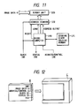
- Fig. 1 is a block diagram of an embodiment of the present invention, applied to a solid-state electronic still camera employing an IC memory.
- Light penetrating a photographing lens 10 enters an image sensor 12 which thus generates RGB signals corresponding to the object.
- a signal processing circuit 14 converts said RGB signals into image data, such as luminance data and color difference data, or converted RGB data. Said signal processing circuit 14 effects parallel-to-serial conversion on said image data, and serially sends said data to a solid-state memory apparatus 16 composed of an IC memory.
- a system control circuit 18 controls various circuit units, including a display device, in response to input signals for example from a shutter switch.
- a timing generator 20 sends a series of sequence timing signals to the signal processing ciucuit 14 and the solid-state memory apparatus 16, in response to the instructions from the system control circuit 18.
- the lens 10, image sensor 12, signal processing circuit 14, system control circuit 18 and timing control circuit 20 are incorporated in the camera body, while the solid-state memory apparatus 16 is detachable therefrom.
- Said solid-state memory apparatus 16 is connected to the camera body through a serial data line 14A, a clock line 14B, an address/control line 14C and a status line 14D.
- a serial data line 14A is connected to the camera body through a serial data line 14A, a clock line 14B, an address/control line 14C and a status line 14D.
- additional lines such as power supply lines and various auxiliary signal lines, but they are omitted in the drawing since they are not directly related to the present invention.
- Fig. 2 shows an example of the internal structure of the solid-state memory apparatus 16, wherein provided are a parallel-serial converter 22; a memory unit 24 composed of a semiconductor memory capable of random access; an address counter 26; a preset value setting ROM 28 for holding the preset value for the address counter 26; a storage state holding memory 30 for holding the storage state of the memory unit 24; a sheet number counter 32; and a timing signal generator 34 for generating various timing signals according the state of a clock lines 16B, an address/control line 16C and a status line 16D.
- power supply lines and various signals lines but those not directly related to the present invention are omitted for the purpose of clarity.
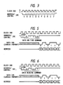
- Fig. 3 is a timing chart of mode setting of the solid-state memory apparatus 16. Correlation between the operating modes and the binary values of A, B, C and D in Fig. 3 is summarized in Table 1.
- the operating mode of the solid-state memory apparatus 16 can be set by sending a predetermined command through the address/control line 16C to the timing generator 34 of the solid-state memory apparatus 16.
- the sheet number counter 32 releases the address for the present value setting ROM 28 holding the start address of address counter 26 for each block.
- the output of the sheet number counter 32 is also used for addressing the storage state holding memory 30.
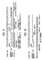
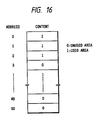
- the storage state holding memory 30 stores 1-bit signals indicating the used/unused state of each block (for example "1" for used and "0" for unused). If the amount of information is 100 Kbytes per image, the memory capacity of the memory unit 24 is Mbytes for 50 images.
- Fig. 16 shows an example of storage state.
- the addresses generated by the address counter 26 can be stepwise increased.
- the addresses to the memory unit 24 are generated from the address counter 26, and the data storage or readout is conducted pixel by pixel in synchronization with the clock signal. Since each pixel of the image has a density range of 6 to 8 bits, the access to the memory unit 24 is simultaneously made for plural bits corresponding to said density range.
- the obtained parallel data are sent to the parallel-serial converter 22 for conversion into serial data.
- the storage into the memory unit 24 is conducted in inverse manner.
- the status line 16B is used for releasing the content of the storage state holding memory 24, but can also be utilized for transmitting timing signals in other functions.
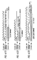
- Fig. 4 is a timing chart for a command signal for setting the sheet number counter 32.
- the signal on the address/control line 16C is sampled at the downshift edge of the clock signal on the clock line 16D.
- the signal on said line 16C is normally in the H-level, but a 4-bit command signal (cf. Tab. 1) following a start bit determines the operating mode. Thereafter the address/control line 16C returns to the H-level state.
- a clear command signal is sent from the camera body (Fig. 4(1)), and, in response, the counter 32 is cleared.
- the used/unused data of the 1st block of the memory unit 24 is read from the storage state holding memory 30 and is sent to the camera body through the status line 16B.
- a count-up command signal is sent from the camera body to the solid state memory apparatus 16, thereby increasing the count of the counter 32 by one.
- the used/unused data of the 2nd block is read from the holding memory 30 and sent to the camera body through the status line 16B.
- the number of empty areas of the memory unit 24 can be confirmed by repeating the above-explained steps.
- a counter down-load command signal is sent from the camera body to the solid-state memory apparatus 16 with the timing shown in Fig. 4(3), followed by a set number "3", thereby designating the 4th block.
- 6 bits are sent in succession from the least significant bit.
- the preset value setting ROM 28 releases the start address of the 4th block.
- Fig. 5 is a timing chart of data storage into memory unit 24.
- a data storage command signal is sent to the solid-state memory apparatus 16 through the address/control line 16C, and the data to be stored are sent through the data line 16A in synchronization with the clock signal on the clock line 16D.
- the address counter 26 is stepped up at the upshift of the clock signal, and the memory unit 24 fetches the data at the downshift of said clock signal.
- the solid-state memory apparatus enters a stand-by state for a next command.
- Fig. 6 is a timing chart for data readout from the memory unit 24.
- the address counter 26 is stepped up at the upshift of the clock signal, and the stored data are read from the memory unit 24 at the downshift of said clock signal.
- the data read from the memory unit 24 are converted into serial signals by the parallel-serial converter 22.
- the camera body and the solid-state memory apparatus 16 are connected by four signal lines, but it is also possible to unit the clock line 16D and the data line 16A, or to expand functions by adding another control line (for example storage disable line).
- the status line 16B is usually used for confirming the content of the storage state holding member 30, but it may naturally be used for other purposes.
- the storage of image data in the memory unit 24 may be made in various modes, such as by NTSC or PAL signals, by luminance and color difference signals, by RGB signals, or by compressed signals.
- the present embodiment enables high-speed access to an arbitrary data block with a limited number of signal lines. Also the host apparatus is relieved from the burden of memory administration and address calculation.
- the serial data line is enough for access because normal operating modes do not involve random access to the solid-state memory apparatus, but a high-speed random access capability is required for each image memory block for example in case of high-speed continuous photographing operation or random reproduction of photographed images.
- the memory apparatus can no longer be used if the image processing method of the camera (for example NTSC, PAL HD, SECAM, Hi-band etc.) is changed, thus varying the data length.
- the image processing method of the camera for example NTSC, PAL HD, SECAM, Hi-band etc.
- the following embodiment allows common use of a memory even if the image processing method of the camera is changed.
- the memory is equipped with means for identifying the image processing method employed in the camera, and with plural address generators.
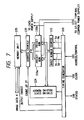
- Fig. 7 is a block diagram of an embodiment of the IC memory apparatus of the present invention
- Fig. 8 shows an example of connection between the memory and the camera.
- the present embodiment provides a solid-state memory apparatus (pack) for NTSC and PAL systems, wherein two preset ROM's 23a, 23b are provided for setting the address counter 22.
- a select signal 23c for said ROM's 23a/b is given by a contact of the electronic camera C.
- the camera C is equipped with a contact indicating the image processing system therein, so that the memory M can automatically iden tify NTSC or PAL system.
- an IC (main) memory 125 capable of random access; an address counter 122; a preset ROM 123a for NTSC system; a preset ROM 123b for PAL system; a strage state holding memory 124; a sheet number counter 121; and a timing signal generator 109.
- the selection of the preset ROM 123a or 123b is automatically made by mounting the memory apparatus M on the camera C as shown in Fig. 8.
- Fig. 8 which is a magnified view of connectors of the memory M and camera C
- the ROM 23a or 23b is automatically selected according to whether a terminal NTSC IN or PAL IN on the camera is powered.
- the camera C releases an access command signal to the storage state holding memory 24 from an address/control terminal 16C, for confirming the presence of an empty space in the memory 124.
- the camera C releases a write command signal from the address/control terminal 16C, and sends out image and audio data 4 in synchronization with the clock signal 16D for successive storage in the memory.
- Fig. 9 is a timing chart showing a representative example of readout of empty area of the storage state holding memory 124
- Fig. 10 is a timing chart showing a representative example of data storage.
- Fig. 11 is a block diagram of an IC memory apparatus constituting a third embodiment of the present invention
- Fig. 12 is an example of the connection between the memory and the camera.
- main memory 125 capable of random access
- address counter 122 an address counter 122
- microcomputer 140 an EEPROM (electrically erasable programmable ROM) 141 serving as the storage state holding memory or an auxiliary memory for the microcomputer 140.
- EEPROM electrically erasable programmable ROM
- the above-explained memory apparatus is used in the following manner.
- the communication to the microcomputer 140 is conducted through the status line 16B and the address/control line 16C, in synchronization with the clock signal 16D from the camera.
- the storage state holding memory 141 composed of the EEPROM stores presence or absence of data in each block of the memory unit 125, number of sizes of memory blocks, total capacity of main memory etc. At the shipment of the memory from the factory, there is only stored the total capacity of memory, and the number of sizes is stored as zero.
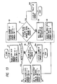
- Fig. 13 is a flow chart of the control sequence of the microcomputer 140 in the present embodiment.
- a step S1 reads the number of block sizes of the memory through the status line 16B. If a step S2 identifies that said number of sizes is zero, a step S3 identifies that the memory apparatus M is unused, and writes a block size suitable for the camera C into the EEPROM 41 through the microcomputer 140. Then a step S4 writes absence of data in the EEPROM 41 for all the blocks.
- step S2 if the step S2 identifies that the number of sizes is not zero, the sequence proceeds to a step S5 for discriminating whether the memory size coincides with the size in the system controller of the camera C, and, if not, a step S5a releases a warning on the camera C, and the writing operation into the memory M is not conducted.
- a step S6 reads the absence/presence of data in each block from the EEPROM 141.
- the camera C enters a stand-by state until the photographing operation in a step S8.
- the camera C sends a write command signal to the microcomputer 140, which, in response, calculates the address by (empty block number x block size), then loads the calculated address into the address counter 122, and releases a ready signal to the status line 16B, whereby the data are stored in succession into the main memory 125 in synchronization with the clock signal 16D.
- a step S10 displays the memory "full" state and the sequence is terminated.
- the present third embodiment does not require additional terminals in comparison with the foregoing second embodiment, and is still adaptable to any block size. It is also possible to prevent erroneous storage into a memory apparatus of different memory block size.
- Fig. 14 shows an example of the content of the storage state holding memory 141 shown in Fig. 11 wherein 150 indicates the number of block sizes, 151 indicate the number of main memory, and 152 and 153 respectively indicate first and second blocks, wherein presence and absence of data are indicated by "1" and "0".
- Fig. 15 shows a third embodiment of the connection of the camera and the IC memory unit of the present invention.
- a pair of mechanical projections 160 are provided on the camera for stabilizing the connection between the memory M and the camera C
- the memory unit M is provided with holes 161a, 161b respectively corresponding to the NTSC and PAL systems.
- said projection 16D engages with either of said holes 161a, 161b, whereby the memory M can detect the characteristic of the camera C, and utilizes the result of said detection for selecting the preset ROM 123a or 123b as in the memory apparatus as shown in Fig. 7.
- the memory M can dispense with additional mechanical structures in such embodiment.
- the present embodiment featured by the presence of plural address generators in the memory apparatus, provides a memory apparatus not fixed to the data size of NTSC or PAL system, so that a same memory apparatus can be utilized regardless of the image processing system of the electronic camera.
- a memory apparatus equipped with a memory capable of random data storage and readout, plural address generators storing start address of each of blocks defined in the memory, a detector for detecting the image processing method used in the input into or output from the memory, and a switching unit for switching the start address of each block according to the output of the detector.
Abstract
Description
- The present invention relates to a memory apparatus and a handling apparatus therefor.
- Electronic still cameras employing magnetic floppy disks as the recording medium are already commercialized, but, owing to the decreasing cost and increasing level of integration of semiconductor memories, there are recently proposed electronic still camera systems employing solid-state memories such as semiconductor memories.
- In the use, as the recording medium, of a solid-state memory apparatus detachable from the camera body and composed of large-capacity IC memories, it is necessary to reduce the number of connecting lines with the camera body and to still enable rapid access. More specifically, the camera body and such solid-state memory apparatus are connected by a serial data line and several control lines for the purpose of achieving simpler connection, higher reliability and lower cost, since the usual parallel structure of data lines and address lines, employed in the incorporated image memory, increases the number of connecting lines, thus deteriorating the reliability and increasing the cost.
- The serial data line is enough for ordinary operating modes which do not require random access to said solid-state memory apparatus, but high-speed random access capability in each image memory unit (block) is required, for example, in high-speed continuous photographing operation or in random reproduction of the photographed images.
- An object of the present invention is to provide an apparatus enabling storage or readout of data to or from a memory apparatus by a simple operation or a simple structure.
- Another object of the present invention is to provide an image processing system and an apparatus constituting said system, capable of confirming the size of image stored in the memory, from the outside.
- Still another object of the present invention is to provide an image processing system and an apparatus therefor, capable of detecting the kind of the memory and thereby effecting satisfactory control on the storage of image data according to the kind of the memory.
- Still another object of the present invention is to provide an apparatus enabling storage or readout of data to or from a memory apparatus with a simple structure and a simple operation regardless of the image processing method.
- The foregoing objects can be attained, according to a preferred embodiment of the present invention, by an apparatus provided with a memory capable of random data storage and readout, plural address generators storing start addresses of blocks in said memory, specy detecting means for detecting the specy of image processing method of the data stored in or read from said memory, and switch means for switching the start address of said block, whereby the address need not be calculated in the access of a designated memory block in the memory. Consequently the host apparatus needs only to send the information designating a memory block for which access is desired, to the solid-state memory apparatus, so that high-speed data transfer is made possible with a limited number of signal lines. Besides a memory can be utilized effectively in common, even if different processing methods are involved.
- The foregoing and still other objects of the present invention, and the advantages thereof, will become fully apparent from the following description of embodiments, which is to be taken in conjunction with the attached drawings.
-
- Fig. 1 is a block diagram of an embodiment of the present invention;
- Fig. 2 is a block diagram of a solid-
state memory apparatus 16 in Fig. 1; - Fig. 3 is a timing chart of command signals for the solid-
state memory apparatus 16; - Fig. 4 is a timing chart of a setting command signal for a sheet number counter 32 in Fig. 2;
- Fig. 5 is a timing chart of a write command signal for a
memory unit 24 in Fig. 2; - Fig. 6 is a timing chart of a read command signal for the
memory unit 24; - Fig. 7 is a block diagram of an IC memory apparatus in a second embodiment of the present invention;
- Fig. 8 is a view showing an example of connection between the IC memory shown in Fig. 7 and a camera;
- Fig. 9 is a timing chart of data reading from a storage state holding memory;
- Fig. 10 is a timing chart of data writing into said memory;
- Fig. 11 is a block diagram of a third embodiment of the present invention;
- Fig. 12 is a view showing an example of connection between the memory unit in Fig. 11 and a camera;
- Fig. 13 is a flow chart showing the control sequence of the third embodiment;
- Fig. 14 is a view showing an example of content of the storage state holding memory shown in Fig. 11;
- Fig. 15 is a view of a fourth embodiment of the connection of memory and camera; and
- Fig. 16 a view showing an example of content of the storage state holding memory.
- Now the present invention will be clarified by embodiments thereof shown in the attached drawings.
- Fig. 1 is a block diagram of an embodiment of the present invention, applied to a solid-state electronic still camera employing an IC memory. Light penetrating a photographing
lens 10 enters animage sensor 12 which thus generates RGB signals corresponding to the object. Asignal processing circuit 14 converts said RGB signals into image data, such as luminance data and color difference data, or converted RGB data. Saidsignal processing circuit 14 effects parallel-to-serial conversion on said image data, and serially sends said data to a solid-state memory apparatus 16 composed of an IC memory. Asystem control circuit 18 controls various circuit units, including a display device, in response to input signals for example from a shutter switch. Atiming generator 20 sends a series of sequence timing signals to thesignal processing ciucuit 14 and the solid-state memory apparatus 16, in response to the instructions from thesystem control circuit 18. - The
lens 10,image sensor 12,signal processing circuit 14,system control circuit 18 andtiming control circuit 20 are incorporated in the camera body, while the solid-state memory apparatus 16 is detachable therefrom. Said solid-state memory apparatus 16 is connected to the camera body through a serial data line 14A, a clock line 14B, an address/control line 14C and a status line 14D. Naturally there are additional lines such as power supply lines and various auxiliary signal lines, but they are omitted in the drawing since they are not directly related to the present invention. - Fig. 2 shows an example of the internal structure of the solid-
state memory apparatus 16, wherein provided are a parallel-serial converter 22; amemory unit 24 composed of a semiconductor memory capable of random access; anaddress counter 26; a presetvalue setting ROM 28 for holding the preset value for theaddress counter 26; a storagestate holding memory 30 for holding the storage state of thememory unit 24; a sheet number counter 32; and atiming signal generator 34 for generating various timing signals according the state of aclock lines 16B, an address/control line 16C and astatus line 16D. There are additionally provided power supply lines and various signals lines, but those not directly related to the present invention are omitted for the purpose of clarity. - Fig. 3 is a timing chart of mode setting of the solid-
state memory apparatus 16. Correlation between the operating modes and the binary values of A, B, C and D in Fig. 3 is summarized in Table 1. The operating mode of the solid-state memory apparatus 16 can be set by sending a predetermined command through the address/control line 16C to thetiming generator 34 of the solid-state memory apparatus 16. The sheet number counter 32 releases the address for the presentvalue setting ROM 28 holding the start address ofaddress counter 26 for each block. The output of the sheet number counter 32 is also used for addressing the storagestate holding memory 30. In case thememory unit 24 has, for example, memory areas for 50 images, or 50 memory blocks, the storagestate holding memory 30 stores 1-bit signals indicating the used/unused state of each block (for example "1" for used and "0" for unused). If the amount of information is 100 Kbytes per image, the memory capacity of thememory unit 24 is Mbytes for 50 images. Fig. 16 shows an example of storage state. - Since the image storage or readout of the
memory unit 24 is conducted in the unit of an image at a time, the addresses generated by theaddress counter 26 can be stepwise increased. Thus the addresses to thememory unit 24 are generated from theaddress counter 26, and the data storage or readout is conducted pixel by pixel in synchronization with the clock signal. Since each pixel of the image has a density range of 6 to 8 bits, the access to thememory unit 24 is simultaneously made for plural bits corresponding to said density range. In case of data readout from thememory unit 24, the obtained parallel data are sent to the parallel-serial converter 22 for conversion into serial data. The storage into thememory unit 24 is conducted in inverse manner. Thestatus line 16B is used for releasing the content of the storagestate holding memory 24, but can also be utilized for transmitting timing signals in other functions. - Fig. 4 is a timing chart for a command signal for setting the sheet number counter 32. The signal on the address/
control line 16C is sampled at the downshift edge of the clock signal on theclock line 16D. The signal on saidline 16C is normally in the H-level, but a 4-bit command signal (cf. Tab. 1) following a start bit determines the operating mode. Thereafter the address/control line 16C returns to the H-level state. For checking the empty areas of the solid-state memory apparatus 16, a clear command signal is sent from the camera body (Fig. 4(1)), and, in response, the counter 32 is cleared. Thus the used/unused data of the 1st block of thememory unit 24 is read from the storagestate holding memory 30 and is sent to the camera body through thestatus line 16B. - Then, as shown in Fig. 4(2), a count-up command signal is sent from the camera body to the solid
state memory apparatus 16, thereby increasing the count of the counter 32 by one. Thus the used/unused data of the 2nd block is read from the holdingmemory 30 and sent to the camera body through thestatus line 16B. The number of empty areas of thememory unit 24 can be confirmed by repeating the above-explained steps. - It is assumed that the first three blocks are already used. In case of image storage, a counter down-load command signal is sent from the camera body to the solid-
state memory apparatus 16 with the timing shown in Fig. 4(3), followed by a set number "3", thereby designating the 4th block. In the example shown in Fig. 4, 6 bits are sent in succession from the least significant bit. Thus the presetvalue setting ROM 28 releases the start address of the 4th block. - Fig. 5 is a timing chart of data storage into
memory unit 24. At first a data storage command signal is sent to the solid-state memory apparatus 16 through the address/control line 16C, and the data to be stored are sent through thedata line 16A in synchronization with the clock signal on theclock line 16D. Theaddress counter 26 is stepped up at the upshift of the clock signal, and thememory unit 24 fetches the data at the downshift of said clock signal. After the image data of an image are stored, the solid-state memory apparatus enters a stand-by state for a next command. - Fig. 6 is a timing chart for data readout from the
memory unit 24. In response to a memory readout command signal, as in the data storage procedure, theaddress counter 26 is stepped up at the upshift of the clock signal, and the stored data are read from thememory unit 24 at the downshift of said clock signal. The data read from thememory unit 24 are converted into serial signals by the parallel-serial converter 22. - In the foregoing embodiment, the camera body and the solid-
state memory apparatus 16 are connected by four signal lines, but it is also possible to unit theclock line 16D and thedata line 16A, or to expand functions by adding another control line (for example storage disable line). Thestatus line 16B is usually used for confirming the content of the storagestate holding member 30, but it may naturally be used for other purposes. The storage of image data in thememory unit 24 may be made in various modes, such as by NTSC or PAL signals, by luminance and color difference signals, by RGB signals, or by compressed signals.Table 1 ABCD OPERATING MODE 0000 clear counter 32 0001 count up counter 32 0010 count down counter 32 0011 down load counter 32 (followed by E - J) 0100 clear memory 0101 read from memory 0110 write into memory 0111 reserve system 1XXX reverse system - As will be easily understood from the foregoing, the present embodiment enables high-speed access to an arbitrary data block with a limited number of signal lines. Also the host apparatus is relieved from the burden of memory administration and address calculation.
- In the foregoing embodiment, the serial data line is enough for access because normal operating modes do not involve random access to the solid-state memory apparatus, but a high-speed random access capability is required for each image memory block for example in case of high-speed continuous photographing operation or random reproduction of photographed images.
- In the following there will be explained another embodiment of the solid-state memory apparatus requiring only a limited number of connecting lines, still having random access capability and enabling to use a common memory regardless of the image processing methods.
- Since the structure shown in Fig. 1 employs a fixed
ROM 28 in the address generator, the memory apparatus can no longer be used if the image processing method of the camera (for example NTSC, PAL HD, SECAM, Hi-band etc.) is changed, thus varying the data length. - On the other hand, the following embodiment allows common use of a memory even if the image processing method of the camera is changed.
- For this purpose, the memory is equipped with means for identifying the image processing method employed in the camera, and with plural address generators.
- Fig. 7 is a block diagram of an embodiment of the IC memory apparatus of the present invention, and Fig. 8 shows an example of connection between the memory and the camera.
- The present embodiment provides a solid-state memory apparatus (pack) for NTSC and PAL systems, wherein two preset ROM's 23a, 23b are provided for setting the
address counter 22. A select signal 23c for said ROM's 23a/b is given by a contact of the electronic camera C. The camera C is equipped with a contact indicating the image processing system therein, so that the memory M can automatically iden tify NTSC or PAL system. - In the structure shown in Fig. 7, there are provided an IC (main)
memory 125 capable of random access; anaddress counter 122; apreset ROM 123a for NTSC system; apreset ROM 123b for PAL system; a stragestate holding memory 124; asheet number counter 121; and atiming signal generator 109. - In the following there will be explained the function of the above-explained embodiment.
- At first, the selection of the
preset ROM state holding memory 24 from an address/control terminal 16C, for confirming the presence of an empty space in thememory 124. After a subsequent photographing operation, the camera C releases a write command signal from the address/control terminal 16C, and sends out image andaudio data 4 in synchronization with theclock signal 16D for successive storage in the memory. - Fig. 9 is a timing chart showing a representative example of readout of empty area of the storage
state holding memory 124, and Fig. 10 is a timing chart showing a representative example of data storage. - Fig. 11 is a block diagram of an IC memory apparatus constituting a third embodiment of the present invention, and Fig. 12 is an example of the connection between the memory and the camera.
- In these drawings, same or equivalent components as in the first embodiment in Figs. 7 and 8 are represented by same numbers.
- There are shown a
main memory 125 capable of random access, anaddress counter 122, amicrocomputer 140, and an EEPROM (electrically erasable programmable ROM) 141 serving as the storage state holding memory or an auxiliary memory for themicrocomputer 140. - The above-explained memory apparatus is used in the following manner. The communication to the
microcomputer 140 is conducted through thestatus line 16B and the address/control line 16C, in synchronization with theclock signal 16D from the camera. The storagestate holding memory 141 composed of the EEPROM stores presence or absence of data in each block of thememory unit 125, number of sizes of memory blocks, total capacity of main memory etc. At the shipment of the memory from the factory, there is only stored the total capacity of memory, and the number of sizes is stored as zero. - Fig. 13 is a flow chart of the control sequence of the
microcomputer 140 in the present embodiment. When the memory M is connected to the camera C, a step S1 reads the number of block sizes of the memory through thestatus line 16B. If a step S2 identifies that said number of sizes is zero, a step S3 identifies that the memory apparatus M is unused, and writes a block size suitable for the camera C into the EEPROM 41 through themicrocomputer 140. Then a step S4 writes absence of data in the EEPROM 41 for all the blocks. On the other hand, if the step S2 identifies that the number of sizes is not zero, the sequence proceeds to a step S5 for discriminating whether the memory size coincides with the size in the system controller of the camera C, and, if not, a step S5a releases a warning on the camera C, and the writing operation into the memory M is not conducted. - If the step S5 identifies that the read memory block size coincides with the size in the camera C, a step S6 reads the absence/presence of data in each block from the
EEPROM 141. As soon as an empty area is detected in a step S7, the camera C enters a stand-by state until the photographing operation in a step S8. Then in a step S9, the camera C sends a write command signal to themicrocomputer 140, which, in response, calculates the address by (empty block number x block size), then loads the calculated address into theaddress counter 122, and releases a ready signal to thestatus line 16B, whereby the data are stored in succession into themain memory 125 in synchronization with theclock signal 16D. If the step S7 identifies the absence of empty block, a step S10 displays the memory "full" state and the sequence is terminated. - As explained in the foregoing, the present third embodiment does not require additional terminals in comparison with the foregoing second embodiment, and is still adaptable to any block size. It is also possible to prevent erroneous storage into a memory apparatus of different memory block size.
- Fig. 14 shows an example of the content of the storage
state holding memory 141 shown in Fig. 11 wherein 150 indicates the number of block sizes, 151 indicate the number of main memory, and 152 and 153 respectively indicate first and second blocks, wherein presence and absence of data are indicated by "1" and "0". - Fig. 15 shows a third embodiment of the connection of the camera and the IC memory unit of the present invention. In the present embodiment a pair of
mechanical projections 160 are provided on the camera for stabilizing the connection between the memory M and the camera C, and the memory unit M is provided with holes 161a, 161b respectively corresponding to the NTSC and PAL systems. As shown in partial magnified view, saidprojection 16D engages with either of said holes 161a, 161b, whereby the memory M can detect the characteristic of the camera C, and utilizes the result of said detection for selecting thepreset ROM - As explained in the foregoing, the present embodiment, featured by the presence of plural address generators in the memory apparatus, provides a memory apparatus not fixed to the data size of NTSC or PAL system, so that a same memory apparatus can be utilized regardless of the image processing system of the electronic camera.
- There is disclosed a memory apparatus equipped with a memory capable of random data storage and readout, plural address generators storing start address of each of blocks defined in the memory, a detector for detecting the image processing method used in the input into or output from the memory, and a switching unit for switching the start address of each block according to the output of the detector.
Claims (24)
input/output means for data input/output of image data into or from said memory.
means for generating addresses ensuing the start address of a memory block released by said block address memory means.
means for controlling the data storage into said memory, according to the detection by said detection means.
Applications Claiming Priority (4)
| Application Number | Priority Date | Filing Date | Title |
|---|---|---|---|
| JP63308169A JPH02154387A (en) | 1988-12-06 | 1988-12-06 | Solid-state memory device |
| JP308169/88 | 1988-12-06 | ||
| JP63309933A JP3016083B2 (en) | 1988-12-09 | 1988-12-09 | Image storage device |
| JP309933/88 | 1988-12-09 |
Publications (3)
| Publication Number | Publication Date |
|---|---|
| EP0372514A2 true EP0372514A2 (en) | 1990-06-13 |
| EP0372514A3 EP0372514A3 (en) | 1992-02-26 |
| EP0372514B1 EP0372514B1 (en) | 1997-03-05 |
Family
ID=26565433
Family Applications (1)
| Application Number | Title | Priority Date | Filing Date |
|---|---|---|---|
| EP89122467A Expired - Lifetime EP0372514B1 (en) | 1988-12-06 | 1989-12-06 | Image pick-up system |
Country Status (3)
| Country | Link |
|---|---|
| US (2) | US5418926A (en) |
| EP (1) | EP0372514B1 (en) |
| DE (1) | DE68927820T2 (en) |
Cited By (4)
| Publication number | Priority date | Publication date | Assignee | Title |
|---|---|---|---|---|
| WO1991011881A1 (en) * | 1990-01-29 | 1991-08-08 | Eastman Kodak Company | Record on command recording in a solid state fast frame recorder |
| EP0523452A1 (en) * | 1991-07-19 | 1993-01-20 | Sharp Kabushiki Kaisha | Recording and reproducing apparatus |
| EP0528280A1 (en) * | 1991-08-09 | 1993-02-24 | Kabushiki Kaisha Toshiba | Memory card apparatus |
| US5450129A (en) * | 1990-07-19 | 1995-09-12 | Canon Kabushiki Kaisha | Image processing apparatus for converting different television standard signals |
Families Citing this family (20)
| Publication number | Priority date | Publication date | Assignee | Title |
|---|---|---|---|---|
| US6487366B1 (en) * | 1990-02-16 | 2002-11-26 | Minolta Co., Ltd. | Camera system capable of storing compressed data |
| US5642458A (en) * | 1992-11-18 | 1997-06-24 | Canon Kabushiki Kaisha | Video signal processing apparatus |
| US5956452A (en) * | 1992-10-19 | 1999-09-21 | Mitsubishi Denki Kabushiki Kaisha | Still picture recording and reproducing apparatus which properly performs recording and reproducing a plurality of different recording formats |
| JP3548191B2 (en) * | 1993-03-22 | 2004-07-28 | キヤノン株式会社 | camera |
| US5874999A (en) * | 1993-04-28 | 1999-02-23 | Fukuyama & Associates | Image processing apparatus with multiple data modes |
| JP3383963B2 (en) * | 1993-12-14 | 2003-03-10 | 富士写真フイルム株式会社 | Method of expanding storage capacity for photographic film and film player |
| JPH08289180A (en) * | 1995-02-14 | 1996-11-01 | Nikon Corp | Electronic still camera |
| US6786420B1 (en) | 1997-07-15 | 2004-09-07 | Silverbrook Research Pty. Ltd. | Data distribution mechanism in the form of ink dots on cards |
| US6618117B2 (en) | 1997-07-12 | 2003-09-09 | Silverbrook Research Pty Ltd | Image sensing apparatus including a microcontroller |
| US6624848B1 (en) | 1997-07-15 | 2003-09-23 | Silverbrook Research Pty Ltd | Cascading image modification using multiple digital cameras incorporating image processing |
| US7110024B1 (en) | 1997-07-15 | 2006-09-19 | Silverbrook Research Pty Ltd | Digital camera system having motion deblurring means |
| US6985207B2 (en) | 1997-07-15 | 2006-01-10 | Silverbrook Research Pty Ltd | Photographic prints having magnetically recordable media |
| US7551201B2 (en) | 1997-07-15 | 2009-06-23 | Silverbrook Research Pty Ltd | Image capture and processing device for a print on demand digital camera system |
| US6879341B1 (en) | 1997-07-15 | 2005-04-12 | Silverbrook Research Pty Ltd | Digital camera system containing a VLIW vector processor |
| US6690419B1 (en) | 1997-07-15 | 2004-02-10 | Silverbrook Research Pty Ltd | Utilising eye detection methods for image processing in a digital image camera |
| AUPO802797A0 (en) | 1997-07-15 | 1997-08-07 | Silverbrook Research Pty Ltd | Image processing method and apparatus (ART54) |
| AUPO850597A0 (en) | 1997-08-11 | 1997-09-04 | Silverbrook Research Pty Ltd | Image processing method and apparatus (art01a) |
| AUPP702098A0 (en) | 1998-11-09 | 1998-12-03 | Silverbrook Research Pty Ltd | Image creation method and apparatus (ART73) |
| AUPQ056099A0 (en) | 1999-05-25 | 1999-06-17 | Silverbrook Research Pty Ltd | A method and apparatus (pprint01) |
| US6661454B1 (en) | 1999-06-14 | 2003-12-09 | Eastman Kodak Company | Digital camera with memory card fullness icon |
Citations (5)
| Publication number | Priority date | Publication date | Assignee | Title |
|---|---|---|---|---|
| JPS6081987A (en) * | 1983-10-12 | 1985-05-10 | Mitsubishi Electric Corp | Picture memory device |
| EP0195608A2 (en) * | 1985-03-18 | 1986-09-24 | Sony Corporation | Terminal apparatus for videotex system |
| DD254095A1 (en) * | 1986-11-28 | 1988-02-10 | Post Rundfunk Fernsehtech | VIDEO STORE ADDRESS CIRCUIT |
| JPS63232689A (en) * | 1987-03-20 | 1988-09-28 | Toshiba Corp | Special reproducing device |
| EP0323194A2 (en) * | 1987-12-25 | 1989-07-05 | Kabushiki Kaisha Toshiba | Electronic still camera and image recording method thereof |
Family Cites Families (18)
| Publication number | Priority date | Publication date | Assignee | Title |
|---|---|---|---|---|
| DE254095C (en) * | ||||
| BE890517A (en) * | 1981-09-28 | 1982-01-18 | Staar Sa | ELECTRONIC IMAGE STORAGE DEVICE |
| JPS5969965A (en) * | 1982-10-15 | 1984-04-20 | Canon Inc | Frame transfer type image pick-up element |
| US4667228A (en) * | 1983-10-14 | 1987-05-19 | Canon Kabushiki Kaisha | Image signal processing apparatus |
| JPS60148289A (en) * | 1984-01-11 | 1985-08-05 | Canon Inc | Image forming device |
| DE3501138A1 (en) * | 1984-01-18 | 1985-07-18 | Canon K.K., Tokio/Tokyo | IMAGE RECORDING DEVICE |
| US4663669A (en) * | 1984-02-01 | 1987-05-05 | Canon Kabushiki Kaisha | Image sensing apparatus |
| US4779137A (en) * | 1986-04-23 | 1988-10-18 | Canon Kabushiki Kaisha | Image pickup apparatus |
| JPS62269581A (en) * | 1986-05-19 | 1987-11-24 | Matsushita Electric Ind Co Ltd | Electronic still camera |
| JPS63143689A (en) * | 1986-12-06 | 1988-06-15 | Tokyo Electric Co Ltd | Capacity detector for memory card |
| JP2529242B2 (en) * | 1987-03-13 | 1996-08-28 | 松下電器産業株式会社 | Electronic camera system |
| JPH07110065B2 (en) * | 1987-05-01 | 1995-11-22 | 富士写真フイルム株式会社 | Digital electronic still camera |
| US4907231A (en) * | 1987-05-06 | 1990-03-06 | Fuji Photo Film Co., Ltd. | Memory cartridge-connectable electronic device such as electronic still video camera |
| US5003506A (en) * | 1987-06-02 | 1991-03-26 | Anritsu Corporation | Memory capacity detection apparatus and electronic applied measuring device employing the same |
| JPS6444587A (en) * | 1987-08-12 | 1989-02-16 | Fuji Photo Film Co Ltd | Memory cartridge |
| US5018017A (en) * | 1987-12-25 | 1991-05-21 | Kabushiki Kaisha Toshiba | Electronic still camera and image recording method thereof |
| US5153729A (en) * | 1988-10-24 | 1992-10-06 | Fuji Photo Film Co., Ltd. | Digital electronic still camera automatically determining conditions of a memory cartridge |
| JP2764677B2 (en) * | 1993-05-17 | 1998-06-11 | 株式会社荏原製作所 | Multi-stage pump |
-
1989
- 1989-12-06 DE DE68927820T patent/DE68927820T2/en not_active Expired - Fee Related
- 1989-12-06 EP EP89122467A patent/EP0372514B1/en not_active Expired - Lifetime
-
1992
- 1992-12-07 US US07/987,240 patent/US5418926A/en not_active Expired - Fee Related
-
1995
- 1995-02-06 US US08/383,850 patent/US5570130A/en not_active Expired - Fee Related
Patent Citations (5)
| Publication number | Priority date | Publication date | Assignee | Title |
|---|---|---|---|---|
| JPS6081987A (en) * | 1983-10-12 | 1985-05-10 | Mitsubishi Electric Corp | Picture memory device |
| EP0195608A2 (en) * | 1985-03-18 | 1986-09-24 | Sony Corporation | Terminal apparatus for videotex system |
| DD254095A1 (en) * | 1986-11-28 | 1988-02-10 | Post Rundfunk Fernsehtech | VIDEO STORE ADDRESS CIRCUIT |
| JPS63232689A (en) * | 1987-03-20 | 1988-09-28 | Toshiba Corp | Special reproducing device |
| EP0323194A2 (en) * | 1987-12-25 | 1989-07-05 | Kabushiki Kaisha Toshiba | Electronic still camera and image recording method thereof |
Non-Patent Citations (2)
| Title |
|---|
| PATENT ABSTRACTS OF JAPAN vol. 13, no. 34 (E-708) 25 January 1989, & JP-A-63 232689 (TOSHIBA) 28 September 1988, * |
| PATENT ABSTRACTS OF JAPAN vol. 9, no. 225 (E-342) 11 September 1985, & JP-A-60 081987 (MITSUBISHI DENKI) 10 May 1985, * |
Cited By (8)
| Publication number | Priority date | Publication date | Assignee | Title |
|---|---|---|---|---|
| WO1991011881A1 (en) * | 1990-01-29 | 1991-08-08 | Eastman Kodak Company | Record on command recording in a solid state fast frame recorder |
| US5140434A (en) * | 1990-01-29 | 1992-08-18 | Eastman Kodak Company | Record on command recording in a solid state fast frame recorder |
| US5450129A (en) * | 1990-07-19 | 1995-09-12 | Canon Kabushiki Kaisha | Image processing apparatus for converting different television standard signals |
| EP0523452A1 (en) * | 1991-07-19 | 1993-01-20 | Sharp Kabushiki Kaisha | Recording and reproducing apparatus |
| US5499316A (en) * | 1991-07-19 | 1996-03-12 | Sharp Kabushiki Kaisha | Recording and reproducing system for selectively reproducing portions of recorded sound using an index |
| EP0528280A1 (en) * | 1991-08-09 | 1993-02-24 | Kabushiki Kaisha Toshiba | Memory card apparatus |
| US5579502A (en) * | 1991-08-09 | 1996-11-26 | Kabushiki Kaisha Toshiba | Memory card apparatus using EEPROMS for storing data and an interface buffer for buffering data transfer between the EEPROMS and an external device |
| EP0772358A1 (en) | 1991-08-09 | 1997-05-07 | Kabushiki Kaisha Toshiba | Memory card apparatus |
Also Published As
| Publication number | Publication date |
|---|---|
| DE68927820T2 (en) | 1997-07-10 |
| EP0372514A3 (en) | 1992-02-26 |
| US5418926A (en) | 1995-05-23 |
| US5570130A (en) | 1996-10-29 |
| DE68927820D1 (en) | 1997-04-10 |
| EP0372514B1 (en) | 1997-03-05 |
Similar Documents
| Publication | Publication Date | Title |
|---|---|---|
| EP0372514A2 (en) | Memory apparatus and handling apparatus therefor | |
| US4237488A (en) | Blemish compensating system for a solid state image pick-up device | |
| US5986700A (en) | Recording operation control device | |
| US8314858B2 (en) | Imaging and recording apparatus controlling erasure of data in flash type memory | |
| US5751350A (en) | Dual mode electronic camera having a large recording capacity | |
| US5633976A (en) | Image recording apparatus and electronic still camera | |
| JPH06350907A (en) | Electronic still camera | |
| US5231514A (en) | Image data processing device | |
| US6118929A (en) | Solid-state camera and solid-state memory apparatus | |
| US6433821B1 (en) | Digital electronic still-video camera, and method of controlling same | |
| JP2776934B2 (en) | Video signal processing device | |
| US20040135901A1 (en) | Imaging and recording apparatus | |
| JP3278182B2 (en) | Image recording apparatus and control method thereof | |
| US5821996A (en) | Solid-sate camera with solid-state memory for holding characteristic code representing characteristic of an internal circuit | |
| EP0464621B1 (en) | Signal processing system using external storage device | |
| JPS63284987A (en) | Electronic still camera | |
| JP4010057B2 (en) | Camera device | |
| JP3528058B2 (en) | Digital still camera | |
| JP3016083B2 (en) | Image storage device | |
| JP2859267B2 (en) | Still image recording device | |
| US7176964B1 (en) | Electronic still camera provided with a display | |
| JPH08195927A (en) | Image reproducing device | |
| JPS63260376A (en) | Camera integrating type video tape recorder | |
| JP2827258B2 (en) | Solid camera | |
| JPH02154387A (en) | Solid-state memory device |
Legal Events
| Date | Code | Title | Description |
|---|---|---|---|
| PUAI | Public reference made under article 153(3) epc to a published international application that has entered the european phase |
Free format text: ORIGINAL CODE: 0009012 |
|
| AK | Designated contracting states |
Kind code of ref document: A2 Designated state(s): DE FR GB |
|
| 17P | Request for examination filed |
Effective date: 19901221 |
|
| PUAL | Search report despatched |
Free format text: ORIGINAL CODE: 0009013 |
|
| AK | Designated contracting states |
Kind code of ref document: A3 Designated state(s): DE FR GB |
|
| 17Q | First examination report despatched |
Effective date: 19940506 |
|
| GRAG | Despatch of communication of intention to grant |
Free format text: ORIGINAL CODE: EPIDOS AGRA |
|
| GRAH | Despatch of communication of intention to grant a patent |
Free format text: ORIGINAL CODE: EPIDOS IGRA |
|
| GRAH | Despatch of communication of intention to grant a patent |
Free format text: ORIGINAL CODE: EPIDOS IGRA |
|
| GRAA | (expected) grant |
Free format text: ORIGINAL CODE: 0009210 |
|
| AK | Designated contracting states |
Kind code of ref document: B1 Designated state(s): DE FR GB |
|
| REF | Corresponds to: |
Ref document number: 68927820 Country of ref document: DE Date of ref document: 19970410 |
|
| ET | Fr: translation filed | ||
| PLBE | No opposition filed within time limit |
Free format text: ORIGINAL CODE: 0009261 |
|
| STAA | Information on the status of an ep patent application or granted ep patent |
Free format text: STATUS: NO OPPOSITION FILED WITHIN TIME LIMIT |
|
| 26N | No opposition filed | ||
| REG | Reference to a national code |
Ref country code: GB Ref legal event code: IF02 |
|
| PGFP | Annual fee paid to national office [announced via postgrant information from national office to epo] |
Ref country code: GB Payment date: 20031203 Year of fee payment: 15 |
|
| PGFP | Annual fee paid to national office [announced via postgrant information from national office to epo] |
Ref country code: FR Payment date: 20031210 Year of fee payment: 15 |
|
| PGFP | Annual fee paid to national office [announced via postgrant information from national office to epo] |
Ref country code: DE Payment date: 20031218 Year of fee payment: 15 |
|
| PG25 | Lapsed in a contracting state [announced via postgrant information from national office to epo] |
Ref country code: GB Free format text: LAPSE BECAUSE OF NON-PAYMENT OF DUE FEES Effective date: 20041206 |
|
| PG25 | Lapsed in a contracting state [announced via postgrant information from national office to epo] |
Ref country code: DE Free format text: LAPSE BECAUSE OF NON-PAYMENT OF DUE FEES Effective date: 20050701 |
|
| GBPC | Gb: european patent ceased through non-payment of renewal fee |
Effective date: 20041206 |
|
| PG25 | Lapsed in a contracting state [announced via postgrant information from national office to epo] |
Ref country code: FR Free format text: LAPSE BECAUSE OF NON-PAYMENT OF DUE FEES Effective date: 20050831 |
|
| REG | Reference to a national code |
Ref country code: FR Ref legal event code: ST |