EP0377988A2 - Wavelength converting optical device - Google Patents
Wavelength converting optical device Download PDFInfo
- Publication number
- EP0377988A2 EP0377988A2 EP89313380A EP89313380A EP0377988A2 EP 0377988 A2 EP0377988 A2 EP 0377988A2 EP 89313380 A EP89313380 A EP 89313380A EP 89313380 A EP89313380 A EP 89313380A EP 0377988 A2 EP0377988 A2 EP 0377988A2
- Authority
- EP
- European Patent Office
- Prior art keywords
- wave
- optical
- face
- waveguide
- respect
- Prior art date
- Legal status (The legal status is an assumption and is not a legal conclusion. Google has not performed a legal analysis and makes no representation as to the accuracy of the status listed.)
- Granted
Links
Images


Classifications
-
- G—PHYSICS
- G02—OPTICS
- G02F—OPTICAL DEVICES OR ARRANGEMENTS FOR THE CONTROL OF LIGHT BY MODIFICATION OF THE OPTICAL PROPERTIES OF THE MEDIA OF THE ELEMENTS INVOLVED THEREIN; NON-LINEAR OPTICS; FREQUENCY-CHANGING OF LIGHT; OPTICAL LOGIC ELEMENTS; OPTICAL ANALOGUE/DIGITAL CONVERTERS
- G02F1/00—Devices or arrangements for the control of the intensity, colour, phase, polarisation or direction of light arriving from an independent light source, e.g. switching, gating or modulating; Non-linear optics
- G02F1/35—Non-linear optics
- G02F1/37—Non-linear optics for second-harmonic generation
- G02F1/377—Non-linear optics for second-harmonic generation in an optical waveguide structure
-
- G—PHYSICS
- G02—OPTICS
- G02B—OPTICAL ELEMENTS, SYSTEMS OR APPARATUS
- G02B27/00—Optical systems or apparatus not provided for by any of the groups G02B1/00 - G02B26/00, G02B30/00
- G02B27/42—Diffraction optics, i.e. systems including a diffractive element being designed for providing a diffractive effect
- G02B27/4233—Diffraction optics, i.e. systems including a diffractive element being designed for providing a diffractive effect having a diffractive element [DOE] contributing to a non-imaging application
-
- G—PHYSICS
- G02—OPTICS
- G02B—OPTICAL ELEMENTS, SYSTEMS OR APPARATUS
- G02B6/00—Light guides; Structural details of arrangements comprising light guides and other optical elements, e.g. couplings
- G02B6/10—Light guides; Structural details of arrangements comprising light guides and other optical elements, e.g. couplings of the optical waveguide type
- G02B6/12—Light guides; Structural details of arrangements comprising light guides and other optical elements, e.g. couplings of the optical waveguide type of the integrated circuit kind
- G02B6/122—Basic optical elements, e.g. light-guiding paths
- G02B6/124—Geodesic lenses or integrated gratings
-
- G—PHYSICS
- G02—OPTICS
- G02B—OPTICAL ELEMENTS, SYSTEMS OR APPARATUS
- G02B6/00—Light guides; Structural details of arrangements comprising light guides and other optical elements, e.g. couplings
- G02B6/24—Coupling light guides
- G02B6/26—Optical coupling means
- G02B6/32—Optical coupling means having lens focusing means positioned between opposed fibre ends
-
- G—PHYSICS
- G02—OPTICS
- G02B—OPTICAL ELEMENTS, SYSTEMS OR APPARATUS
- G02B6/00—Light guides; Structural details of arrangements comprising light guides and other optical elements, e.g. couplings
- G02B6/24—Coupling light guides
- G02B6/26—Optical coupling means
- G02B6/34—Optical coupling means utilising prism or grating
-
- G—PHYSICS
- G02—OPTICS
- G02B—OPTICAL ELEMENTS, SYSTEMS OR APPARATUS
- G02B27/00—Optical systems or apparatus not provided for by any of the groups G02B1/00 - G02B26/00, G02B30/00
- G02B27/09—Beam shaping, e.g. changing the cross-sectional area, not otherwise provided for
- G02B27/0938—Using specific optical elements
- G02B27/0944—Diffractive optical elements, e.g. gratings, holograms
-
- G—PHYSICS
- G02—OPTICS
- G02F—OPTICAL DEVICES OR ARRANGEMENTS FOR THE CONTROL OF LIGHT BY MODIFICATION OF THE OPTICAL PROPERTIES OF THE MEDIA OF THE ELEMENTS INVOLVED THEREIN; NON-LINEAR OPTICS; FREQUENCY-CHANGING OF LIGHT; OPTICAL LOGIC ELEMENTS; OPTICAL ANALOGUE/DIGITAL CONVERTERS
- G02F1/00—Devices or arrangements for the control of the intensity, colour, phase, polarisation or direction of light arriving from an independent light source, e.g. switching, gating or modulating; Non-linear optics
- G02F1/35—Non-linear optics
- G02F1/37—Non-linear optics for second-harmonic generation
- G02F1/372—Means for homogenizing the output beam
-
- G—PHYSICS
- G02—OPTICS
- G02F—OPTICAL DEVICES OR ARRANGEMENTS FOR THE CONTROL OF LIGHT BY MODIFICATION OF THE OPTICAL PROPERTIES OF THE MEDIA OF THE ELEMENTS INVOLVED THEREIN; NON-LINEAR OPTICS; FREQUENCY-CHANGING OF LIGHT; OPTICAL LOGIC ELEMENTS; OPTICAL ANALOGUE/DIGITAL CONVERTERS
- G02F1/00—Devices or arrangements for the control of the intensity, colour, phase, polarisation or direction of light arriving from an independent light source, e.g. switching, gating or modulating; Non-linear optics
- G02F1/35—Non-linear optics
- G02F1/37—Non-linear optics for second-harmonic generation
- G02F1/374—Cherenkov radiation
-
- G—PHYSICS
- G02—OPTICS
- G02F—OPTICAL DEVICES OR ARRANGEMENTS FOR THE CONTROL OF LIGHT BY MODIFICATION OF THE OPTICAL PROPERTIES OF THE MEDIA OF THE ELEMENTS INVOLVED THEREIN; NON-LINEAR OPTICS; FREQUENCY-CHANGING OF LIGHT; OPTICAL LOGIC ELEMENTS; OPTICAL ANALOGUE/DIGITAL CONVERTERS
- G02F1/00—Devices or arrangements for the control of the intensity, colour, phase, polarisation or direction of light arriving from an independent light source, e.g. switching, gating or modulating; Non-linear optics
- G02F1/35—Non-linear optics
- G02F1/37—Non-linear optics for second-harmonic generation
- G02F1/377—Non-linear optics for second-harmonic generation in an optical waveguide structure
- G02F1/383—Non-linear optics for second-harmonic generation in an optical waveguide structure of the optical fibre type
Definitions
- the present invention relates to a wavelength converting optical device for obtaining a light source for short wavelengths used for optical information processing or optical measurement equipments and, more particularly, to a wavelength converting optical device using a Cerenkov radiation system.
- Coherent light sources for short wavelengths have recently been developed for the purpose of application to high-density optical disk systems, measurement/display systems, and the like.
- a short wavelength light source is indispensable to a high-density optical disk system.
- a semiconductor laser as a short wavelength light source is compact and lightweight and has low power consumption. Because of these advantages, semiconductor lasers for shorter wavelengths using new materials have been developed.
- An InGaAtP semiconductor laser having an oscillation wavelength in the 0.6-am band (red) has already reached the level of practical application.
- semiconductor lasers for oscillating light beams having shorter wavelengths, such as green or blue light beams have been studied, no laser capable of continuous-wave oscillation at room temperature has been obtained yet, and hence practical application of such a laser is not warranted.
- SHG second harmonic generation
- a nonlinear optical crystal into a waveguide by using a semiconductor laser as a fundamental wave light source.
- a blue light beam (x 2 ) of 1 mW as a second harmonic wave was obtained with respect to a semiconductor laser beam with a fundamental wave ( ⁇ 1 ) of 80 mW, by using a proton-exchange LiNb0 3 waveguide having a waveguide portion formed on an LiNb0 3 substrate (T.
- a light output of at least several mW must be obtained.
- a light output of 100 mW or more is required as a fundamental wave.
- the laser tends to be degraded due to the influences of heat, COD (catastrophic optical damage), and the like. Therefore, a long-term reliability is difficult to ensure. This poses a serious limitation in practical use of a short wavelength light source using the SHG system.
- an external cavity system is considered as a means for increasing the conversion efficiency from a fundamental wave to an optical second harmonic wave. It is reported that an optical second harmonic wave of 29.7 mW is obtained with respect to, e.g., a light output of 52.6 mW as a fundamental wave by using this system (W.J. Kozlovsky et al., IEEE J. Quantum Electron., Vol-24, No. 6, pp. 913 - 919 (1988)). In this system, however, a YAG laser excited by a semiconductor laser is used as a fundamental wave, and the excitation semiconductor laser must have a light output of 500 mW. On the other hand, resonator type SHG in an optical waveguide has been reported.
- a Cerenkov radiation beam has a complex wave front due to radiation from axially distributed light sources. More specifically, a Cerenkov radiation beam is constituted by divergent light having different beam waist positions depending on output positions and hence does not have axial symmetry for the case of LiNb0 3 waveguide. For this reason, in order to collimate or focus the radiation beam, a special optical system is required. In addition, it is difficult to decrease the spot size of the beam to a diffraction limit.
- a waveguide for this SHG has a coaxial structure in which a nonlinear crystal core is covered with a glass cladding.
- This output beam has axial symmetry, but cannot be directly collimated or focused.
- the present invention has been made in consideration of the above situation, and has its object to provide a wavelength converting optical device having a high conversion efficiency without phase matching adjustment.
- a reflecting film is formed on an end face of an optical waveguide so as to increase conversion efficiency from a fundamental wave to an optical second harmonic wave.
- a wave front converting element for converting a conical wave into a plane wave or spherical wave is formed on a light output end face of an optical waveguide so as to collimate or focus an optical second harmonic beam emitted from the light output end face of the optical waveguide.
- a device which comprises an optical waveguide having a waveguide portion and a cladding portion at least one of which is formed of a nonlinear optical material, for converting a fundamental wave, incident on the waveguide portion from one end face of the optical waveguide, into an optical second harmonic wave by Cerenkov radiation, radiating the second harmonic wave onto the cladding portion, and outputting the optical second harmonic wave radiated on the cladding portion from the other end face of the optical waveguide; and a reflecting film formed on at least an optical second harmonic emerging end face of the optical waveguide, the reflecting film having a high reflectivity with respect to a fundamental wave of a guided mode and having a low reflectivity with respect to the optical second harmonic wave.
- a wavelength converting optical device for collimating or focusing an optical second harmonic wave which comprises a wavelength converting portion, having an optical waveguide including a waveguide portion and a cladding portion, at least one of which is formed of a nonlinear optical material, for converting a fundamental wave, incident on the waveguide portion from one end face of the optical waveguide, into an optical second harmonic wave by Cerenkov radiation, radiating the optical harmonic wave onto the clad portion, and outputting the optical second harmonic wave radiated on the cladding portion from the other end face of the optical waveguide; and a wave front converting portion, provided at the other end face of the waveguide, for converting the second harmonic wave emitted from the other end face into a plane wave, a spherical wave, or a conical wave having different divergence angles.
- optical waveguide type SHG using a Cerenkov radiation system by forming the above-described reflecting film on the end face of the optical waveguide, optical power in the optical waveguide can be increased, and hence the conversion efficiency from a fundamental wave to an optical second harmonic wave can be increased.
- the wave front converting portion is provided at the end face of the optical waveguide, an optical second harmonic wave as a plane wave (collimated light) or a spherical wave (converging or diverging light) can be obtained, thus allowing effective use of an optical second harmonic beam.
- the optical waveguide is constituted as a fiber optical waveguide, a wavelength converting optical device comprising a wave front converting portion, which can be easily manufactured and allows easy positioning, can be realized by using a concentrical diffraction grating as the wave front converting portion provided at the light emerging end face of the waveguide.
- a wavelength converting optical device comprising a wave front converting portion having a high diffraction efficiency can be realized by using a diffraction grating with a sawtooth section.
- Figs. 1 and 2 show a wavelength converting optical device according to a first embodiment of the present invention.
- the converting device comprises an optical waveguide 10 designed as a fiber type optical waveguide having axial symmetry.
- the waveguide 10 has a core (optical waveguide portion) 11 formed of a nonlinear material and having a circular section, and a cylindrical glass cladding 12 coated on the core 11.
- the waveguide 10 has output and input end faces 10a and 10b perpendicular to the axis of the waveguide.
- First and second reflecting films 14 and 13 are respectively bonded to these end faces.
- a fundamental wave 15 enters from the input end face 10b into the core 11 through the reflecting film 13, and a Cerenkov radiation beam (optical second harmonic wave) 16 propagating in the cladding 12 emerges from the output end face 10a on which the reflecting film 14 is formed.
- the refractive indices of the core 11 and the cladding 12 are set so as to cause an incident fundamental wave and a second harmonic wave to become a guided mode and a Cerenkov radiation beam, respectively.
- a material for the cladding 12 is selected to satisfy where n EFF is the effective refractive index of the fiber type optical waveguide 10 having the core 11 and the cladding 12 with respect to the fundamental wave.
- the fundamental wave 15 having the wavelength X When the fundamental wave 15 having the wavelength X, is incident on the optical waveguide 10, the wave is converted into an optical second harmonic wave having a wavelength ⁇ 1 /2 by the core 11 formed of a nonlinear optical material, and propagates in the cladding 12 as the Cerenkov radiation beam 16 having an angle 8c with respect to the core 11.
- the values ⁇ c , n EFF , and n 2 satisfy the following relation:
- the first and second reflecting films 14 and 13 serve to reflect a guided mode which is not converted into a second harmonic wave and to cause it to resonate, as will be described later. That is, the converting device is designed as a resonator type converting device.
- the first reflecting film 14 is designed to have a high reflectivity with respect to a fundamental wave as a guided mode and have a low reflectivity with respect to an optical second harmonic wave as a Cerenkov radiation beam.
- the reflectivity of the reflecting film 14 is ideally set to be 100% with respect to a fundamental wave, but is preferably set to be 95% or more, or still more preferably, 99% or more.
- the reflectivity with respect to a second harmonic wave is ideally set to be 0%, but is preferably set at 5% or less, or more preferably 2% of less.
- the second reflecting film 13 is designed to have an optimal reflectivity as a resonator with respect to a fundamental wave as a guided mode, as will be described below.
- the reflectivities of the reflecting films 13 and 14 with respect to a fundamental wave (guided mode) are respectively r, and r 2 ; the power of an incident fundamental wave, P 1 ; the coupling efficiency with respect to the optical waveguide 10, ⁇ ; the power of the guided mode immediately after it is incident on the optical waveguide, P c ; the conversion efficiency to a Cerenkov radiation beam, ⁇ sH ⁇ P c ; a ratio of power (with respect to a waveguide length L) lost by guided mode loss other than the conversion, a; and a power to be externally output as an optical second harmonic wave, P 2 .
- a conventional system for second harmonic generation by means of Cerenkov radiation i.e., a system without the reflecting films 13 and 14, if reflection by the end faces of a waveguide is ignored, the following relations are established between the above parameters:
- P. and P 2 are given by the following equations under resonance conditions (IEEE. J. Quantum Electron, QE-24,6, pp. 913 -919 (1988)): where t 2 is the transmittance of the first reflecting film 14 with respect to an optical second harmonic wave, and t is a function of P c , which is given by the following equation:
- the impedance matching condition of the resonator with respect to an incident wave is given as:
- the second reflecting film 13 has a reflectivity set in the above-described manner, a guided mode which is reflected by the first reflecting film 14 without being converted into a second harmonic wave is reflected by the second reflecting film 13 and propagates toward the output end face 10a through the core 11 again. In this case, part of the guided mode is converted into a second harmonic wave and emerges from the output end face 10a.
- an output of 1 mW is obtained as an optical second harmonic output with the parameters according to equation (4).
- t 2 1, the light output of an optical second harmonic wave is 11.4 mW. Therefore, the optical second harmonic wave power obtained in this arrangement is ten times that of the arrangement without reflecting films.
- the reflectivity of each reflecting film can be set in the above-described manner by using a dielectric multilayer.
- a conversion efficiency of about 10% is obtained; 90% of the incident wave power is not converted into a second harmonic wave propagating toward the end face 10a.
- 90% of the incident wave power is not converted into a second harmonic wave propagating toward the end face 10a.
- 50% is not coupled to the optical waveguide, 30% is lost by waveguide loss, and 10% is converted into an optical second harmonic wave propagating in the opposite direction.
- the coupling efficiency with respect to the optical waveguide is increased and the waveguide loss is decreased, a wavelength converting optical device having a higher conversion efficiency can be realized.
- the loss per unit length may be decreased, or the waveguide length may be shortened.
- a decrease in waveguide loss to 0.5 dB/cm is equivalent to a decrease in waveguide length to 2.5 mm in terms of an increase in conversion efficiency.
- the power of an incident wave can be set to be a smaller value.
- a light output of 30 mW is a general value for a GaAtAs laser used as a light source for a write-once type disk, and hence such an SHG system can be realized.
- the reflecting films 13 and 14 are provided on both the end faces of the fiber type optical waveguide to form a resonator, a guided mode power in the optical waveguide 10 can be increased. For this reason, the fundamental wave can be effectively converted into a Cerenkov radiation beam in the optical waveguide 10, and a conversion efficiency can be greatly increased to about ten times that of a conventional system. Since it is possible to decrease the incidence power, the device of this embodiment can be effectively used as a short wavelength light source having a light output of several mW even by using a currently available semiconductor laser. In addition, the device can be realized with a very simple arrangement obtained by merely providing the reflecting films 13 and 14 on both end faces of the optical waveguide 10.
- a resonator is formed by providing the reflecting films on both end faces of the optical waveguide.
- the conversion efficiency can be increased by providing a reflecting film on only the output end face.
- a semiconductor laser 18 is used as a light source for generating a fundamental wave, and a resonance effect may be obtained between the first reflecting film 14 of the converting device and a reflecting film 20 of the semiconductor laser.
- Fig. 4 shows a wavelength converting optical device according to the second embodiment of the present invention.
- the second embodiment is equivalent to the first embodiment in terms of its structure, but is different therefrom in the function of the second reflecting film 13. More specifically, in the first embodiment, half of an optical second harmonic wave generated by Cerenkov radiation propagates to the input end face 10b of the waveguide 10 and is wasted. In contrast to this, in the second embodiment, the optical second harmonic wave propagating to the incidence end face side is reflected by the reflecting film 13 so as to cause the wave to propagate toward the end face 10a of the waveguide 10.
- an output twice that of the first embodiment e.g., an optical second harmonic wave output of 6 mW or more can be obtained with respect to a fundamental wave of 30 mW.
- the reflectivity of the second reflecting film 13 with respect to a fundamental wave as a guided mode may be set to be the same value as that of the first embodiment, and the reflectivity with respect to an optical second harmonic wave as a Cerenkov radiation beam may be set to be 100%.
- the respective ideal values can be summarized as follows: where ( ⁇ ) and (2 ⁇ ) are respectively the reflectivities with respect to a fundamental wave and an optical second harmonic wave.
- the reflectivity of the second reflecting film 13 with respect to a fundamental wave is preferably set within the range of 50 to 95%.
- Table shows the design of each reflecting film (dielectric multilayer) for the above specification.
- a center wavelength X o is a value normalized by the wavelength of a fundamental wave
- H and L respectively represent high- and low-refractive-index layers having an optical thickness of ⁇ 0 /4.
- Actual thicknesses t H and t L of these layers are given by the following equations: where n H and n L are the refractive indices of the respective layers, and the following relationship is established between B H and 0 L and a Cerenkov radiation angle ⁇ c .
- the dielectric multilayers shown in Table respectively have a bandpass filter and a short-wavelength- pass filter as their fundamental structures.
- Figs. 5A and 5B respectively correspond to the dielectric multilayers denoted by (a) and (b) in Table.
- the actual reflectivities of the dielectric multilayers for the specification represented by equation (9) are: As is apparent from a comparison between equations (9) and (12), the multilayers can be designed to substantially satisfy the reflectivity characteristics of the specification. In this case, calculations are performed assuming that the value 8c is small and a second harmonic wave is perpendicularly incident on the first and second reflecting films. However, reflectivity design can be performed in consideration of incidence angles and the difference in reflectivity between a radiation mode (optical second harmonic wave) and a guided mode (fundamental wave).
- a structure having axial symmetry (fiber type optical waveguide) is exemplified.
- an optical waveguide a diffusion type optical waveguide or a three-dimensional optical waveguide such as a ridge stripe type optical waveguide may be used.
- an optical second harmonic wave to be output from the end face of the optical waveguide is a conical wave, and hence cannot be directly collimated or focused.
- the second harmonic wave can be converted into a plane or spherical wave.
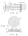
- Figs. 6 to 8 show a third embodiment of the present invention.
- the same reference numerals in the third embodiment denote the same parts as in the second embodiment, and a detailed description thereof will be omitted.
- a wavelength converting optical device comprises a fiber type optical waveguide (wavelength converting portion) 10 which has a core (waveguide portion) 11 formed of a nonlinear material and covered with a glass cladding 12.
- First and second reflecting films 14 and 13 are respectively attached to output and input end faces 10a and 10b of the waveguide 10.
- a lens plate (wave front converting portion) 31 having a diffraction grating of a concentrical pattern serving as a wave front converting element is arranged in contact with the first reflecting film 14.
- Refractive indices ni and n 2 of the cladding 12 and an effective refractive index n EFF of the optical waveguide 10 with respect to a fundamental wave are selected to satisfy equation (1) described above.
- a radiation angle 8c of a Cerenkov radiation beam 16 with respect to the core 11 is given by equation (2).
- the first and second reflecting films 14 and 13 are designed in the same manner as in the second embodiment.
- the optical second harmonic wave 16 emerging from the optical waveguide 10 is converted into a parallel light beam 17 by the lens plate 31.
- This parallel light beam 17 can be focused into a diffraction-limited spot by a conventional convex lens, unlike a light beam diverging in the form of a ring.
- the lens plate 31 includes a concentric diffraction grating 32 having grooves formed at equal intervals.
- a grating pitch A of the diffraction grating 32 is set to satisfy where m is a positive integer.
- an optical second harmonic wave 16 emerging from the end face of the fiber type optical waveguide 10 is converted into a collimated light beam 17 by m-th order diffraction of the diffraction grating 32 of the lens plate 31.
- Figs. 7 and 8 show a structure of the diffraction grating 32.
- the lens plate 31 includes a disk-like substrate 34.
- the diffraction grating 32 is formed on the incidence surface of the substrate.
- An anti-reflecting coating film 35 for preventing reflection of a harmonic wave in the substrate is bonded to the emerging surface of the diffraction grating 32.
- the lens plate 31 is arranged such that the center of diffraction grating 32 coincides with the central axis of the waveguide 10.
- the diffraction grating 32 has a sawtooth sectional shape, as shown in Fig. 8.
- An inclination angle 0 of each tooth at the sawtooth diffraction grating section is set to satisfy the following equation: where n s is the refractive index of the substrate 34, and ⁇ 0 is the propagation angle of a second harmonic wave emerging from the output end face 10a of the optical waveguide 10 in air.
- the following relationship is established between the propagation angle ⁇ 0 and the radiation angle ⁇ c by Cerenkov radiation:
- a depth t of each groove of the diffraction grating 32 can be given by the following equation according to equations (14) and (15):
- the grating 32 can be easily formed by using, e.g., a computer-controlled lathe (NC lathe).
- NC lathe computer-controlled lathe
- a metal die may be formed by means of NC lathe, and the grating 32 can be copied by using a plastic replica technique.
- the value ⁇ c can be decreased by properly selecting a cladding material.
- the conversion efficiency from a fundamental wave into a second harmonic wave can be increased in the same manner as in the second embodiment, and moreover the second harmonic wave can be collimated and output. Therefore, the converting device according to the third embodiment is very effective as a short wavelength light source using a semiconductor laser.
- Fig. 9 shows another method of manufacturing a concentric diffraction grating by using holographic interference exposure.
- reference numeral 40 denotes a truncated cone prism; 41, a diffraction grating substrate; and 42, a photosensitive emulsion layer.
- a central part of a plane wave incident on the bottom surface of the prism 40 propagates straight, whereas a peripheral part of the plane wave is refracted by a prism side surface to become a conical wave.
- Both the parts of light reach a surface of the emulsion layer 42, and a concentric diffraction grating is recorded on the surface by holographic interference.
- a bottom angle 8p of the prism 40 may be selected as follows:
- the lens plate 31 which is an optical element called an axicon
- a conical wave can be converted into a plane wave by using another typical axicon such as a conical prism.
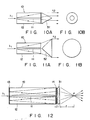
- a ring-like beam can be converted into a plane wave by a conical prism 51 as shown in Fig. 10A.
- the collimated light still has a ring-like shape, as shown in Fig. 10B.
- a method of arranging a conical prism 52 in the direction opposite to that in Fig. 10A as shown in Fig. 11 A may be considered.
- a collimated beam is not a beam having a hollow central portion.
- the prism 52 since only one point of the prism 52 is brought into contact with the output end face of the optical waveguide 10, positioning becomes difficult.
- the direction of light refracted by a side surface of the conical prism is determined by the bottom angle of the prism, considerably strict prism process precision is required.
- a wave front converting element constituted by a concentric diffraction grating can be attached in tight contact with the fiber type optical waveguide 10, output light does not become a ring-like beam having a hollow central portion as shown in Fig. 10B, and the difficulty in positioning shown in Fig. 11A can be eliminated.
- Figs. 12 to 14 show a schematic arrangement of a fourth embodiment of the present invention.
- a lens plate (wave front converting element) 31 is designed to focus an optical second harmonic wave emerging from the output end face of a fiber type optical waveguide 10 on one point.
- a phase n of a diffraction grating 32 of the element 31 is represented by the following equation as a function of a distance r from the center: where L(r) is the optical path length from a point on the diffraction grating surface to a focal point F.
- the optical path length L(r) is given by using a thickness t and a refractive index ns of a substrate 34 of the wave surface converting element 31 as follows (Appl.
- Equations (19) to (23) are substituted by -f, the resultant equations represent a wave front converting element for converting radiated light into light diverging from a point separated from the emerging surface of the substrate 34 by the distance f.
- Figs. 15 to 17 show an embodiment in which this wave front converting element is used.
- Figs. 13 and 14 and Figs. 16 and 17 respectively show patterns of diffraction gratings 32 of the wave front converting elements 31 according to the fourth and fifth embodiments.
- a diffraction grating can be formed by machining using an NC lathe in the same manner as in the third embodiment.
- the diffraction grating 32 is formed on the incidence surface side of the wave surface converting element 31.
- a diffraction grating may be formed on the emerging surface side of the substrate.
- Fig. 18 shows the sixth embodiment of the present invention, in which a diffraction grating 32 having a concentric pattern is formed on the light emerging side of a substrate 34 of a wave front converting element 31.
- the flat bottom surface of the substrate 34 can be bonded to the emerging end face of a fiber type optical waveguide 10.
- a wavelength converting optical device using a Cerenkov radiation system by using a wave front converting element on which a diffraction grating is formed, an optical second harmonic wave emitted from a fiber type optical waveguide can be collimated or focused.
- a wavelength converting optical device including a wave front converting element which can be easily formed and allows easy positioning, can be realized. If the grating pitch of this concentric diffraction grating is set to satisfy equation (13) or (22), an optical second harmonic wave can be converted into a plane wave (collimated light) or spherical wave (converging or diverging light).
- the sectional shape of the concentric diffraction grating is formed into a sawtooth blazed pattern, a wavelength converting optical element, including a wave front converting element having a high refractive index, can be realized.
- the grating pitch of the wave front converting element shown in Figs. 7 and 8 can be given by equation (13).
- the above grating constant can be realized.
- concentric diffraction gratings are formed by machining which enables mass production using a plastic replica, it is difficult to process a diffraction grating having a grating pitch of 1 um or less.
- a technique of performing wave front conversion not only once, but two or more times, may be employed so as to increase the grating pitch of each wave front converting surface, thus facilitating formation of a wave front converting element.
- Figs. 19 to 23 respectively show the seventh to eleventh embodiments based on this idea.
- a substrate 34 of a wave front converting element 31 has two wave front converting surfaces 31 a and 31 b.
- the surfaces 31 a and 31 are respectively constituted by concentric diffraction gratings 32a and 32b, each having grooves formed at equal intervals.
- a wave front converting element 31 includes two substrates 34a and 34b. Concentric diffraction gratings 32a and 32b, each having a grating pitch given by equation (25), are respectively formed on the substrates 34a and 34b. In this case, since the bottom surfaces of the substrates 34a and 34b, which have identical concentric diffraction gratings, need only be bonded to each other, formation of the wave front converting element is further facilitated.
- two diffraction gratings have the same grating pitch.
- a wave front converting element 31 may be constituted by a combination of a concentric diffraction grating 32 and a conical prism 36, as shown in a ninth embodiment of Fig. 21.
- the converting element 31 can be reduced in size as compared with the ones shown in Figs. 10A and 11 A, and moreover positioning is facilitated.
- Fig. 22 shows a tenth embodiment, in which a wave front converting element 31 is constituted by a combination of a concentric diffraction grating 32a having grooves formed at equal intervals and a Fresnel type concentric diffraction grating 32b.
- output light can be converted into a spherical wave converging on one point.
- the grating pitch can be increased as compared with the case wherein conversion is realized by only one wave front converting surface, thus formation of an element is facilitated.
- a concentric diffraction grating 32 having grooves formed at equal intervals and located at the incidence side of a wave converting element 31 may be combined with a spherical or aspherical lens 38 located at the emerging side.
- the wave front converting element is constituted by two or more wave front converting surfaces, a wavelength converting optical device, including a wave front converting element which can be easily processed by machining, can be realized.
- the optical waveguide having an axially symmetrical structure is exemplified as a fiber type optical waveguide.
- the present invention is not limited to this. That is, a three-dimensional optical waveguide such as a diffusion type optical waveguide, an embedded type optical waveguide, or a ridge stripe structure may be used.
- an optical waveguide 10 comprises a rectangular parallel-piped LiNb0 3 substrate 12 as a cladding portion, and a plate-like waveguide portion 11 bonded to a surface of the substrate 12.
- the optical waveguide 10 has input and output end faces 10b and 10a. These end faces extend perpendicular to the optical axis of incident light 15.
- a lens plate 31 as a wave front converting element is arranged to oppose the output end face 10a of the optical waveguide 10.
- the fundamental wave 15 is incident into the waveguide portion 11 through the input end face 10b, and a Cerenkov radiation beam (optical second harmonic wave) 16 propagating in the substrate 12 emerges from the end face 10a of the waveguide 10. Furthermore, the Cerenkov radiation beam 16 is converted into a collimated beam 17 by the wave front converting element 31.
- an optical second harmonic wave as a Cerenkov radiation beam is radiated from the waveguide portion 11 into only the substrate 12 side.
- n EFF the effective refractive index of the optical waveguide 10 with respect to the fundamental wave. Since LiNb0 3 has a large nonlinear optical constant d 33 , a substrate orientation and propagation and polarization directions of the fundamental wave are selected so as to use the constant d 33 .
- a guided mode of a fundamental wave is set to a TM mode propagating in y direction (or x direction). If an x-cut substrate (or y-cut substrate) is used, a guided mode of a fundamental wave is set to be a TE mode propagating in y direction (or x direction).
- the incident light is converted into an optical second harmonic wave having a wavelength of Xi/2 by a nonlinear optical effect of the LiNb0 3 , and propagates in the substrate 12 as the Cerenkov radiation beam 16 having an angle ⁇ c with respect to the waveguide portion 11.
- the following relationship is established between the angle ⁇ c and n 2 :
- This Cerenkov radiation beam is refracted by the output end face 10a and is radiated in the air at an angle eo.
- the following relationship is established between ⁇ 0 and ⁇ c :
- the second harmonic wave radiated in the air is converted into a collimated beam 17 by the wave front converting element 31.
- This collimated beam 17 can be focused into a diffraction-limited spot by a conventional lens.
- the second harmonic wave radiated from the waveguide 10 having the above-described arrangement does not become a perfectly conical wave. This is because the refractive index of a nonlinear crystal generally varies depending on propagation and polarization directions. That is, the emerging angle of the second harmonic wave radiated in the LiNb0 3 substrate 12 varies depending on directions, and the wave dose not have axial symmetry.
- the wave front converting element 31 comprises a rectangular substrate 34 having a diffraction grating 32 arranged to oppose the emerging end face of the waveguide 10.
- the diffraction grating 32 is constituted by part of an elliptic pattern such that equivalent radial grating pitches are changed in accordance with the divergence angle of the second harmonic wave.
- this elliptic pattern is formed such that its major axis coincides with the upper edge of the substrate 34.
- This diffraction grating 32 has grating pitches A 1 and A 2 in two orthogonal directions.
- a refractive index ellipsoid shown in Fig. 27 will be considered first to obtain the refractive index of the substrate 12 with respect to a second harmonic wave.
- the propagation direction of a fundamental wave of guided mode is x
- a vector n1 is given in the same direction as the polarization direction of the guided mode.
- a pointing vector s represents the propagation direction of the second harmonic wave.
- a vector, which has the same propagation direction as that of the second harmonic wave and whose absolute value represents the refractive index with respect to the second harmonic wave, is given as n2 .
- the vector s is represented by the following equation: If n1 and n2 are: then, the respective vectors must satisfy the following relations: where no and n e are respectively the refractive indices with respect to ordinary and extraordinary light waves at the wavelength of the second harmonic wave.
- the refractive index n 2 with respect to the second harmonic wave can be given by the following equation according to equations (30) to (35):
- the value ⁇ in the above equation corresponds to the Cerenkov radiation angle ⁇ c in the arrangement shown in Fig. 24. Since n 2 in equation (36) must satisfy equation (28), the value ⁇ c can be given by the following equation according to equations (28) and (36):
- the Cerenkov radiation angle ⁇ c generally varies depending on an angle ⁇ .
- the angle corresponds to the angle with respect to a waveguide surface when the x-cut substrate and TE mode are used, or corresponds to its complementary angle when the z-cut substrate and TM mode are used.
- the angle ⁇ 0 of the second harmonic wave radiated from the output end face 10a of the waveguide 10 varies depending on ⁇ .
- n e When LiNb0 3 is used, no and n e can be given by the following equations as functions of a wavelength ⁇ [ ⁇ m] and a temperature T [K], respectively (H. V. Hobden et al.: Phys. Lett., Vol. 23, No. 3, pp. 243 - 244 (1966)):
- Fig. 28 shows wavelength dependence of the refractive index of LiNb0 3 at room temperature (25 °C).
- Fig. 28 shows relationships between n 1 , n 2 , and n EFF in equations (27) to (29) when the wavelengths of a fundamental wave and the second harmonic wave are respectively set to be 0.84 ⁇ m and 0.42 ⁇ m.
- Fig. 29 shows relationships between AN and radiation angles of second harmonic waves in the substrate and in the air, which are calculated by using the above equations.
- AN represents the difference between the effective refractive index and the substrate refractive index with respect to the guided mode, and is given as:
- Fig. 29 shows two cases wherein in equation (37) is 0 and ⁇ /2.
- the grating pitch of a diffraction grating used as a wave front converting element for collimating the corresponding light can be given by the following equation:
- a large grating pitch A is preferable in terms of a diffraction grating process.
- AN in order to obtain large grating pitch A, AN must be increased.
- AN 0.135
- n EFF ( ⁇ ) n e ( ⁇ 2)
- A ⁇ .
- Such a diffraction grating can be formed by, e.g., electron beam lithography (G. Hatakoshi et al.: Appl. Opt., Vol. 24, No. 24, pp. 4307 - 4311 (1985)).
- the diffraction grating shown in Figs. 25 and 26 has a sawtooth section, i.e., a blazed pattern so as to increase the diffraction efficiency.
- a diffraction grating can be formed by dose control during electron beam drawing.
- the grating pitch of the diffraction grating varies in different radial directions.
- grating pitches can be set in accordance with the divergence angle of a second harmonic beam in different radial directions.
- an optical second harmonic wave having no axial symmetry can be collimated or focused.
- the wave front converting element serves to collimate output light.
- a wave front converting element for converting output light into a convergent or divergent spherical wave can be formed by changing the grating pattern.
- the grating pattern has an elliptic shape as in he twelfth embodiment.
- this grating has grooves formed at different intervals.
- first and second reflecting films 14 and 13 each having the same structure as that of the reflecting film in the second embodiment may be respectively bonded to emerging and incidence end faces 10a and 10b of an optical waveguide 10 having the same structure as that of the above-described twelfth embodiment. In this case, a conversion efficiency from a guided mode into a second harmonic wave can be increased.
- the diffraction grating of the twelfth embodiment can be formed by electron beam lithography.
- the grating has an elliptic pattern, it is difficult to form the grating by other methods such as machining.
- a diffraction grating having a concentric pattern can be relatively easily formed by using an NC lathe.
- such a diffraction grating having a concentric pattern is used as a wave front converting element in the converting device having the arrangement of the twelfth embodiment, it is difficult to collimate or focus a second harmonic output beam which does not have axial symmetry.
- Figs. 32 to 34 show a wavelength converting device according to a fourteenth embodiment of the present invention.
- This device employs a diffraction grating having a concentric pattern as a wave front converting element 31. More specifically, the device comprises an optical waveguide 10 having an LiNb0 3 substrate 12 and a waveguide 11, and the wave front converting element 31 arranged to oppose an output end face 10a of the waveguide 10.
- the converting element 31 has a rectangular substrate 34 and a diffraction grating 32 formed on its incidence surface.
- the diffraction grating 32 is constituted by part of a concentric pattern.
- the diffraction grating 32 is formed such that the center of the concentric pattern is located at an upper edge of the substrate 34.
- the output end face 10a of the waveguide 10 and the wave front converting element 31, i.e., the diffraction grating 32 are inclined at predetermined angles with respect to a plane perpendicular to the optical axis of incident light 15.
- the anisotropy of a Cerenkov radiation angle from the waveguide 10 can be corrected.
- the inclination angles of the concentric grating 32 and the end face 10a are respectively represented by ⁇ and ⁇ .
- the above equation is modified by using equations (28), (29), and the like as follows: where ⁇ 01 and 0 02 have the same meanings as those in equations (38) and (39).
- the pitch A, given by equation (45) is used as the grating pitch A, and ⁇ 01 and 0 02 are exchanged in the above equation.
- the fourteenth embodiment having the above-described arrangement since the output end face 10a of the optical waveguide 10 and the diffraction grating 32 of the wave front converting element 31 are inclined at the predetermined angles with respect to the plane perpendicular to the optical axis of the incidence light 15, the grating pitches of the diffraction grating can be set in accordance with the divergence angle of the second harmonic beam in different radial directions even by using the diffraction grating having a concentric pattern. Therefore, collimation or focusing of the second harmonic wave which does not have axial symmetry can be performed in the same manner as with the case wherein a diffraction grating having an elliptic pattern is used. In addition, since a diffraction grating having a concentric pattern can be used, a wave front converting element can be easily manufactured.
- both the wave front converting element and the output end face of the waveguide are inclined.
- the anisotropy of a Cerenkov radiation angle can be corrected in the same manner even by inclining only one of them.
- a fifteenth embodiment of the present invention shown in Fig. 35 an output end face 10a of an optical waveguide 10 is arranged to be perpendicular to the optical axis of incident light 15, and a wave front converting element 31 having a diffraction grating 32 with a concentric pattern is inclined with respect to the end face 10a, thereby correcting a Cerenkov radiation angle.
- B (1-cos ⁇ 02 ) 2 + sin 2 ⁇ 02 - sin 2 ⁇ 01 .
- the sign of ⁇ varies depending on whether the z-cut substrate or the x-cut substrate is used. More specifically, in equation (49), ⁇ ⁇ 0, wherein in equation (24), ⁇ > 0.
- Fig. 36 shows a relationship between AN and 0 defined by equation (42).
- a sixteenth embodiment shown in Fig. 37 only an output end face 10a of a waveguide 10 is inclined at a predetermined angle with respect to the plane perpendicular to the optical axis of incident light 15, and a wave front converting element 31 is arranged to be perpendicular to the optical axis.
- ⁇ 0 in equation (48)
- an inclination angle ⁇ of the end face 10a is obtained as follows (a z-cut substrate and a TM mode are used): Similarly, if an x-cut substrate and a TE mode are used,
- Fig. 38 shows a relationship between AN and W.
- an anisotropy correcting effect of a Cerenkov radiation angle is increased with & than with ⁇ . That is, a smaller inclination angle is required when the output end face of the optical waveguide is inclined than when the wave front converting element is inclined. As AN is increased, this tendency becomes more conspicuous.
- Fig. 39 shows a seventeenth embodiment of the present invention, in which both the output end face 10a of a waveguide 10 and a wave front converting element 31 are inclined in the same direction with respect to the plane perpendicular to the optical axis of incident light 15.
- a second harmonic wave emerging from each optical waveguide 10 can be collimated or focused by using a wave front converting element having a diffraction grating with a concentric pattern which can be relatively easily formed.
- Fig. 41 is a perspective view showing a schematic arrangement of an eighteenth embodiment of present invention.
- an embedded type three-dimensional waveguide is used as a fiber type optical waveguide, and a cover made of the same material as that of a substrate is fixed to the upper portion of the optical waveguide so as to further improve axial symmetry.
- the optical waveguide 10 comprises a rectangular parallel-piped LiNb0 3 substrate 12, a cylindrical waveguide portion 11 embedded in the substrate, and a rectangular parallel-piped LiNb0 3 cover 38 fixed to the upper surface of the substrate.
- a wave front converting element 31 is arranged on an output end face 10a of the waveguide 10.
- a diffraction grating having a concentric pattern or an elliptic pattern may be used as the element 31.
- the embedded type three-dimensional optical waveguide in this embodiment can be formed by, e.g., a combination of Ti diffusion and MgO additional diffusion (1986 Spring Applied Physics Meeting, 3p-L-11).
- an inorganic nonlinear material such as LiTaO 3 , KNb0 3 , Li10 3 , or KTP or an organic nonlinear material such as MNA or DAN may be used as a nonlinear material used for a cladding portion, a substrate, and the like of an optical waveguide in place of LiNbO 3 .
- the arrangement of an optical waveguide is not limited to those in the above-described embodiments.
- a waveguide portion may be formed by diffusing an impurity in a surface portion of a substrate formed of a nonlinear material.
- a waveguide portion and a clad portion (substrate) of an optical waveguide is formed of a nonlinear optical material. Therefore, a waveguide portion need not be always formed of a nonlinear optical material, and only cladding portion may be formed of a nonlinear optical material. Alternatively, both waveguide and cladding portions may be formed of a nonlinear optical material.
Landscapes
- Physics & Mathematics (AREA)
- General Physics & Mathematics (AREA)
- Optics & Photonics (AREA)
- Nonlinear Science (AREA)
- Engineering & Computer Science (AREA)
- Microelectronics & Electronic Packaging (AREA)
- Optical Modulation, Optical Deflection, Nonlinear Optics, Optical Demodulation, Optical Logic Elements (AREA)
- Optical Couplings Of Light Guides (AREA)
Abstract
Description
- The present invention relates to a wavelength converting optical device for obtaining a light source for short wavelengths used for optical information processing or optical measurement equipments and, more particularly, to a wavelength converting optical device using a Cerenkov radiation system.
- Coherent light sources for short wavelengths have recently been developed for the purpose of application to high-density optical disk systems, measurement/display systems, and the like. In an optical disk system, since the spot size of a light beam focused on a disk surface is proportional to the wavelength of the light source, a short wavelength light source is indispensable to a high-density optical disk system.
- A semiconductor laser as a short wavelength light source is compact and lightweight and has low power consumption. Because of these advantages, semiconductor lasers for shorter wavelengths using new materials have been developed. An InGaAtP semiconductor laser having an oscillation wavelength in the 0.6-am band (red) has already reached the level of practical application. Although semiconductor lasers for oscillating light beams having shorter wavelengths, such as green or blue light beams, have been studied, no laser capable of continuous-wave oscillation at room temperature has been obtained yet, and hence practical application of such a laser is not warranted.
- As another means for realizing a short wavelength light source, second harmonic generation (SHG) using a nonlinear optical crystal is available, and various studies on SHG have been made. Especially, in SHG, in order to realize a compact, low-power-consumption light source, an attempt has been made to form a nonlinear optical crystal into a waveguide by using a semiconductor laser as a fundamental wave light source. For example, a blue light beam (x2) of 1 mW as a second harmonic wave was obtained with respect to a semiconductor laser beam with a fundamental wave (λ1) of 80 mW, by using a proton-exchange LiNb03 waveguide having a waveguide portion formed on an LiNb03 substrate (T. Taniuchi et al., Extended Abstracts (The 48th Autumn Meeting, 1987); The Japan Society of Applied Physics, 19p-ZG-4). In this system, a second harmonic wave is radiated into a waveguide substrate by Cerenkov radiation. This system is advantageous over the conventional SHG system in that phase matching by angle control, temperature control, or the like is not required.
- For practical applications of such a wavelength converting optical element as a short wavelength light source, a light output of at least several mW must be obtained. For this purpose, a light output of 100 mW or more is required as a fundamental wave. As the output of a semiconductor laser is increased, the laser tends to be degraded due to the influences of heat, COD (catastrophic optical damage), and the like. Therefore, a long-term reliability is difficult to ensure. This poses a serious limitation in practical use of a short wavelength light source using the SHG system.
- In bulk SHG, an external cavity system is considered as a means for increasing the conversion efficiency from a fundamental wave to an optical second harmonic wave. It is reported that an optical second harmonic wave of 29.7 mW is obtained with respect to, e.g., a light output of 52.6 mW as a fundamental wave by using this system (W.J. Kozlovsky et al., IEEE J. Quantum Electron., Vol-24, No. 6, pp. 913 - 919 (1988)). In this system, however, a YAG laser excited by a semiconductor laser is used as a fundamental wave, and the excitation semiconductor laser must have a light output of 500 mW. On the other hand, resonator type SHG in an optical waveguide has been reported. In this case, a conversion efficiency of 0.1% to a second harmonic wave is obtained using Ar laser light as a fundamental wave (R. Reginer et al.: ECOC'86 (1986)). However, in order to realize resonator type SHG in an optical waveguide, both resonation conditions and phase matching conditions must be satisfied. Hence, strict temperature control precision is required. This poses a serious limitation to the practical use of this system.
- In an arrangement in which the above-described proton-exchange LiNb03 waveguide is used, a Cerenkov radiation beam has a complex wave front due to radiation from axially distributed light sources. More specifically, a Cerenkov radiation beam is constituted by divergent light having different beam waist positions depending on output positions and hence does not have axial symmetry for the case of LiNb03 waveguide. For this reason, in order to collimate or focus the radiation beam, a special optical system is required. In addition, it is difficult to decrease the spot size of the beam to a diffraction limit.
- In contrast to this, as a system using the same Cerenkov radiation system, SHG by a single-crystal fiber made of a nonlinear material is reported (T. Yamada et al., Extended Abstracts (The 47th Autumn Meeting, 1986); The Japan Society of Applied Physics, 29a-X-2). A waveguide for this SHG has a coaxial structure in which a nonlinear crystal core is covered with a glass cladding. An optical second harmonic wave becomes Cerenkov radiation light propagating in the cladding at a predetermined angle θc with respect to the optical axis, and a beam emerging from a fiber end face becomes a ring-like beam diverging at an angle 00 with respect to the optical axis (00 = sin-1(n2sinθc), where n2 is the refractive index of the cladding with respect to the optical second harmonic wave). This output beam has axial symmetry, but cannot be directly collimated or focused.
- As described above, in the conventional SHG system using an optical waveguide for a compact system, a satisfactory conversion efficiency has not yet been obtained, and a light output of 100 mW or more is required as a fundamental wave. In addition, in the system using a resonator type optical waveguide for high efficiency, since strict temperature control precision is required for phase matching, its practical use is difficult.
- In the SHG system using Cerenkov radiation requiring no phase matching, it is difficult to collimate or focus the output beam. Moreover, in the fiber system capable of obtaining a beam having axial symmetry, the output beam cannot be directly collimated. Even if collimation is performed by using a special optical system, strict process precision of optical elements is required.
- The present invention has been made in consideration of the above situation, and has its object to provide a wavelength converting optical device having a high conversion efficiency without phase matching adjustment.
- It is another object of the present invention to provide a wavelength converting optical device which can collimate or focus an optical second harmonic beam generated by Cerenkov radiation, without using a special optical system.
- According to the present invention, a reflecting film is formed on an end face of an optical waveguide so as to increase conversion efficiency from a fundamental wave to an optical second harmonic wave. In addition, a wave front converting element for converting a conical wave into a plane wave or spherical wave is formed on a light output end face of an optical waveguide so as to collimate or focus an optical second harmonic beam emitted from the light output end face of the optical waveguide.
- According to the present invention, there is provided a device which comprises an optical waveguide having a waveguide portion and a cladding portion at least one of which is formed of a nonlinear optical material, for converting a fundamental wave, incident on the waveguide portion from one end face of the optical waveguide, into an optical second harmonic wave by Cerenkov radiation, radiating the second harmonic wave onto the cladding portion, and outputting the optical second harmonic wave radiated on the cladding portion from the other end face of the optical waveguide; and a reflecting film formed on at least an optical second harmonic emerging end face of the optical waveguide, the reflecting film having a high reflectivity with respect to a fundamental wave of a guided mode and having a low reflectivity with respect to the optical second harmonic wave.
- In addition, according to the present invention, there is provided a wavelength converting optical device for collimating or focusing an optical second harmonic wave, which comprises a wavelength converting portion, having an optical waveguide including a waveguide portion and a cladding portion, at least one of which is formed of a nonlinear optical material, for converting a fundamental wave, incident on the waveguide portion from one end face of the optical waveguide, into an optical second harmonic wave by Cerenkov radiation, radiating the optical harmonic wave onto the clad portion, and outputting the optical second harmonic wave radiated on the cladding portion from the other end face of the optical waveguide; and a wave front converting portion, provided at the other end face of the waveguide, for converting the second harmonic wave emitted from the other end face into a plane wave, a spherical wave, or a conical wave having different divergence angles.
- According to the present invention, in optical waveguide type SHG using a Cerenkov radiation system, by forming the above-described reflecting film on the end face of the optical waveguide, optical power in the optical waveguide can be increased, and hence the conversion efficiency from a fundamental wave to an optical second harmonic wave can be increased.
- Further, according to the present invention, since the above-described wave front converting portion is provided at the end face of the optical waveguide, an optical second harmonic wave as a plane wave (collimated light) or a spherical wave (converging or diverging light) can be obtained, thus allowing effective use of an optical second harmonic beam. Furthermore, if the optical waveguide is constituted as a fiber optical waveguide, a wavelength converting optical device comprising a wave front converting portion, which can be easily manufactured and allows easy positioning, can be realized by using a concentrical diffraction grating as the wave front converting portion provided at the light emerging end face of the waveguide. Moreover, a wavelength converting optical device comprising a wave front converting portion having a high diffraction efficiency can be realized by using a diffraction grating with a sawtooth section.
- This invention can be more fully understood from the following detailed description when taken in conjunction with the accompanying drawings, in which:
- Figs. 1 and 2 show a wavelength converting optical device according to a first embodiment of the present invention, in which Fig. 1 is a perspective view of the device and Fig. 2 is a sectional view showing a schematic arrangement of the device;
- Fig. 3 is a sectional view showing a schematic arrangement of a modification of the first embodiment;
- Figs. 4 to 5B show a wavelength converting optical device according to a second embodiment of the present invention, in which Fig. 4 is a sectional view showing a schematic arrangement of the device, Fig. 5A is a graph showing a relationship between the normalized wavelength and reflectivity of a second reflecting film, and Fig. 5B is a graph showing a relationship between the normalized wavelength and reflectivity of a first reflecting film;
- Figs. 6 to 9 show a wavelength converting optical device according to a third embodiment of the present invention, in which Fig. 6 is a sectional view showing a schematic arrangement of the device, Fig. 7 is a top view of a wave front converting element, Fig. 8 is a sectional view of the wave front converting element, and Fig. 9 is a view for explaining a method of forming the wave front converting element;
- Figs. 10A and 10B are sectional and front views, respectively, showing a first comparative example wherein a prism is used as a wave front converting element;
- Figs. 11A and 11B are sectional and front views, respectively, showing a second comparative example wherein a prism is used as a wave surface converting element;
- Figs. 12 to 14 show a wavelength converting optical device according to a fourth embodiment of the present invention, in which Fig. 12 is a sectional view showing a schematic arrangement of the device, and
- Figs. 13 and 14 are top and sectional views, respectively, showing a wave front converting element;
- Figs. 15 to 17 show a wavelength converting optical device according to a fifth embodiment of the present invention, in which Fig. 15 is a sectional view showing a schematic arrangement of the device, and
- Figs. 16 and 17 are front and sectional views, respectively, showing a wave front converting element;
- Fig. 18 is a sectional view showing a schematic arrangement of a wavelength converting optical device according to a sixth embodiment of the present invention;
- Fig. 19 is a sectional view showing a schematic arrangement of a wavelength converting optical device according to a seventh embodiment of the present invention;
- Fig. 20 is a sectional view showing a schematic arrangement of a wavelength converting optical device according to an eighth embodiment of the present invention;
- Fig. 21 is a sectional view showing a schematic arrangement of a wavelength converting optical device according to a ninth embodiment of the present invention;
- Fig. 22 is a sectional view showing a schematic arrangement of a wavelength converting optical device according to a tenth embodiment of the present invention;
- Fig. 23 is a sectional view showing a schematic arrangement of a wavelength converting optical device according to an eleventh embodiment of the present invention;
- Figs. 24 to 26 show a wavelength converting optical device according to a twelfth embodiment of the present invention, in which Fig. 24 is a perspective view showing a schematic arrangement of the device, and Figs. 25 and 26 are plan and front views, respectively, showing a wave front converting element;
- Fig. 27 is a view for explaining the refractive index of LiNb03;
- Fig. 28 is a graph showing a relationship between the refractive index and wavelength of LiNb03;
- Fig. 29 is a graph showing a relationship between the Cerenkov radiation angle and ΔN;
- Fig. 30 is a graph showing a relationship between the grating pitch of a wave front converting element and ΔN;
- Fig. 31 is a perspective view showing a schematic arrangement of a wavelength converting optical device according to a thirteenth embodiment of the present invention;
- Figs. 32 to 34 show a wavelength converting optical device according to a fourteenth embodiment of the present invention, in which Fig. 32 is a sectional view showing a schematic arrangement of the device, and Figs. 33 and 34 are plan and front views, respectively, showing a wave front converting element;
- Fig. 35 and 36 show a wavelength converting optical device according to a fifteenth embodiment of the present invention, in which Fig. 35 is a sectional view showing a schematic arrangement of the device, and Fig. 36 is a graph showing a relationship between the inclination angle ϕ and ΔN;
- Figs. 37 and 38 show a wavelength converting optical device according to a sixteenth embodiment of the present invention, in which Fig. 37 is a sectional view showing a schematic arrangement of the device, and Fig. 38 is a graph showing a relationship between the inclination angle ϕ and ΔN;
- Figs. 39 and 40 show a wavelength converting optical device according to a seventeenth embodiment of the present invention, in which Fig. 39 is a sectional view showing a schematic arrangement of the device, and Fig. 40 is a graph showing a relationship between the inclination angle cp and ΔN; and
- Fig. 41 is a perspective view showing a schematic arrangement of a wavelength converting optical device according to an eighteenth embodiment of the present invention.
- Embodiments of the present invention will be described in detail with reference to the accompanying drawings.
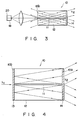
- Figs. 1 and 2 show a wavelength converting optical device according to a first embodiment of the present invention. The converting device comprises an
optical waveguide 10 designed as a fiber type optical waveguide having axial symmetry. Thewaveguide 10 has a core (optical waveguide portion) 11 formed of a nonlinear material and having a circular section, and acylindrical glass cladding 12 coated on thecore 11. Thewaveguide 10 has output and input end faces 10a and 10b perpendicular to the axis of the waveguide. First and second reflectingfilms fundamental wave 15 enters from theinput end face 10b into the core 11 through the reflectingfilm 13, and a Cerenkov radiation beam (optical second harmonic wave) 16 propagating in thecladding 12 emerges from the output end face 10a on which the reflectingfilm 14 is formed. - The refractive indices of the
core 11 and thecladding 12 are set so as to cause an incident fundamental wave and a second harmonic wave to become a guided mode and a Cerenkov radiation beam, respectively. In this case, if the refractive indices of thecladding 12 with respect to wavelengths λ1 and \2 -(= λ1/2) of thefundamental wave 15 and the optical secondharmonic wave 16 are respectively set to be ni and n2, a material for thecladding 12 is selected to satisfy
optical waveguide 10 having the core 11 and thecladding 12 with respect to the fundamental wave. - When the
fundamental wave 15 having the wavelength X, is incident on theoptical waveguide 10, the wave is converted into an optical second harmonic wave having a wavelength λ1/2 by the core 11 formed of a nonlinear optical material, and propagates in thecladding 12 as theCerenkov radiation beam 16 having an angle 8c with respect to thecore 11. The values θc, nEFF, and n2 satisfy the following relation:
- The first and second reflecting
films - The first reflecting
film 14 is designed to have a high reflectivity with respect to a fundamental wave as a guided mode and have a low reflectivity with respect to an optical second harmonic wave as a Cerenkov radiation beam. The reflectivity of the reflectingfilm 14 is ideally set to be 100% with respect to a fundamental wave, but is preferably set to be 95% or more, or still more preferably, 99% or more. The reflectivity with respect to a second harmonic wave is ideally set to be 0%, but is preferably set at 5% or less, or more preferably 2% of less. On the other hand, the second reflectingfilm 13 is designed to have an optimal reflectivity as a resonator with respect to a fundamental wave as a guided mode, as will be described below. - Assume that the reflectivities of the reflecting
films optical waveguide 10, η; the power of the guided mode immediately after it is incident on the optical waveguide, Pc; the conversion efficiency to a Cerenkov radiation beam, γsH·Pc; a ratio of power (with respect to a waveguide length L) lost by guided mode loss other than the conversion, a; and a power to be externally output as an optical second harmonic wave, P2. In a conventional system for second harmonic generation by means of Cerenkov radiation, i.e., a system without the reflectingfilms 

- In contrast to this, in the system with the reflecting
films 

film 14 with respect to an optical second harmonic wave, and t is a function of Pc, which is given by the following equation:

- If the second reflecting
film 13 has a reflectivity set in the above-described manner, a guided mode which is reflected by the first reflectingfilm 14 without being converted into a second harmonic wave is reflected by the second reflectingfilm 13 and propagates toward the output end face 10a through the core 11 again. In this case, part of the guided mode is converted into a second harmonic wave and emerges from the output end face 10a. - Example 1 will be considered, in which = 0.5, ysH = 0.4/W, P, = 100 mW, L = 5 mm, and a waveguide loss a = 1 dB/cm (a to 0.1). When no reflecting film is present, an output of 1 mW is obtained as an optical second harmonic output with the parameters according to equation (4). In contrast to this, if the reflecting films are present, and r2 = 1, the reflectivity of the second reflecting
film 13, which satisfies the impedance matching condition, is given as r, = 0.7 according to equations (5), (7), and (8). If t2 = 1, the light output of an optical second harmonic wave is 11.4 mW. Therefore, the optical second harmonic wave power obtained in this arrangement is ten times that of the arrangement without reflecting films. Note that the reflectivity of each reflecting film can be set in the above-described manner by using a dielectric multilayer. - In example 1, a conversion efficiency of about 10% is obtained; 90% of the incident wave power is not converted into a second harmonic wave propagating toward the end face 10a. Of the incident wave power of 100 mW, 50% is not coupled to the optical waveguide, 30% is lost by waveguide loss, and 10% is converted into an optical second harmonic wave propagating in the opposite direction. As the coupling efficiency with respect to the optical waveguide is increased and the waveguide loss is decreased, a wavelength converting optical device having a higher conversion efficiency can be realized. In order to decrease the waveguide loss, the loss per unit length may be decreased, or the waveguide length may be shortened. In the above-described example, for example, a decrease in waveguide loss to 0.5 dB/cm is equivalent to a decrease in waveguide length to 2.5 mm in terms of an increase in conversion efficiency. In this case, the impedance matching condition is given as ri = 0.75, and, at this time, an optical second harmonic wave power of 16.4 mW is obtained.
- Since a high conversion efficiency can be obtained in the resonator type SHG system, the power of an incident wave can be set to be a smaller value. When a. L = 0.25 dB and an incident wave power is set to be 30 mW, an impedance matching condition is given as r, = 0.83, and an optical second harmonic wave power is 3.1 mW. That is, even if the fundamental wave power is set to be 30 mW and the coupling efficiency with respect to the optical waveguide is 50%, a conversion efficiency of 10% can be obtained. A light output of 30 mW is a general value for a GaAtAs laser used as a light source for a write-once type disk, and hence such an SHG system can be realized.
- As described above, in the first embodiment, since the reflecting
films optical waveguide 10 can be increased. For this reason, the fundamental wave can be effectively converted into a Cerenkov radiation beam in theoptical waveguide 10, and a conversion efficiency can be greatly increased to about ten times that of a conventional system. Since it is possible to decrease the incidence power, the device of this embodiment can be effectively used as a short wavelength light source having a light output of several mW even by using a currently available semiconductor laser. In addition, the device can be realized with a very simple arrangement obtained by merely providing the reflectingfilms optical waveguide 10. - In this embodiment, a resonator is formed by providing the reflecting films on both end faces of the optical waveguide. However, the conversion efficiency can be increased by providing a reflecting film on only the output end face. For example, as shown in Fig. 3, a
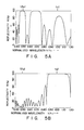
semiconductor laser 18 is used as a light source for generating a fundamental wave, and a resonance effect may be obtained between the first reflectingfilm 14 of the converting device and a reflectingfilm 20 of the semiconductor laser. - Fig. 4 shows a wavelength converting optical device according to the second embodiment of the present invention. In this embodiment, the same parts as in the first embodiment are represented by the same reference numerals, and a detailed description thereof will be omitted. The second embodiment is equivalent to the first embodiment in terms of its structure, but is different therefrom in the function of the second reflecting
film 13. More specifically, in the first embodiment, half of an optical second harmonic wave generated by Cerenkov radiation propagates to theinput end face 10b of thewaveguide 10 and is wasted. In contrast to this, in the second embodiment, the optical second harmonic wave propagating to the incidence end face side is reflected by the reflectingfilm 13 so as to cause the wave to propagate toward the end face 10a of thewaveguide 10. - According to such an arrangement, an output twice that of the first embodiment, e.g., an optical second harmonic wave output of 6 mW or more can be obtained with respect to a fundamental wave of 30 mW. In this case, the reflectivity of the second reflecting
film 13 with respect to a fundamental wave as a guided mode may be set to be the same value as that of the first embodiment, and the reflectivity with respect to an optical second harmonic wave as a Cerenkov radiation beam may be set to be 100%. In this case, the respective ideal values can be summarized as follows:
film 13 with respect to a fundamental wave is preferably set within the range of 50 to 95%. The following Table shows the design of each reflecting film (dielectric multilayer) for the above specification.
- In this Table, a center wavelength Xo is a value normalized by the wavelength of a fundamental wave, and H and L respectively represent high- and low-refractive-index layers having an optical thickness of λ0/4. Actual thicknesses tH and tL of these layers are given by the following equations:


- The dielectric multilayers shown in Table respectively have a bandpass filter and a short-wavelength- pass filter as their fundamental structures. Figs. 5A and 5B respectively show wavelength characteristics of these dielectric multilayers when nH = 2.3(Ti02) and nL = 1.46(Si02). Figs. 5A and 5B respectively correspond to the dielectric multilayers denoted by (a) and (b) in Table. In Figs. 5A and 5B, values normalized by a wavelength X, of a fundamental wave are plotted along each abscissa axis. Wavelengths X/Xi = 1 and λ/λ1 = 0.5 respectively correspond to a fundamental wave (ω) and an optical second harmonic wave (2ω). The actual reflectivities of the dielectric multilayers for the specification represented by equation (9) are:

- In the embodiments described with reference to Figs. 1 and 4, a structure having axial symmetry (fiber type optical waveguide) is exemplified. However, as an optical waveguide, a diffusion type optical waveguide or a three-dimensional optical waveguide such as a ridge stripe type optical waveguide may be used.
- In addition, in the first and second embodiments, an optical second harmonic wave to be output from the end face of the optical waveguide is a conical wave, and hence cannot be directly collimated or focused. However, if an optical element (wave front converting element) to be described later is used, the second harmonic wave can be converted into a plane or spherical wave.
- Figs. 6 to 8 show a third embodiment of the present invention. The same reference numerals in the third embodiment denote the same parts as in the second embodiment, and a detailed description thereof will be omitted.
- A wavelength converting optical device comprises a fiber type optical waveguide (wavelength converting portion) 10 which has a core (waveguide portion) 11 formed of a nonlinear material and covered with a
glass cladding 12. First and second reflectingfilms waveguide 10. In addition, according to the third embodiment, a lens plate (wave front converting portion) 31 having a diffraction grating of a concentrical pattern serving as a wave front converting element is arranged in contact with the first reflectingfilm 14. Refractive indices ni and n2 of thecladding 12 and an effective refractive index nEFF of theoptical waveguide 10 with respect to a fundamental wave are selected to satisfy equation (1) described above. A radiation angle 8c of aCerenkov radiation beam 16 with respect to thecore 11 is given by equation (2). The first and second reflectingfilms - In this embodiment, the optical second
harmonic wave 16 emerging from theoptical waveguide 10 is converted into aparallel light beam 17 by thelens plate 31. This parallellight beam 17 can be focused into a diffraction-limited spot by a conventional convex lens, unlike a light beam diverging in the form of a ring. - The
lens plate 31 includes aconcentric diffraction grating 32 having grooves formed at equal intervals. A grating pitch A of thediffraction grating 32 is set to satisfy
harmonic wave 16 emerging from the end face of the fiber typeoptical waveguide 10 is converted into acollimated light beam 17 by m-th order diffraction of thediffraction grating 32 of thelens plate 31. Figs. 7 and 8 show a structure of thediffraction grating 32. In this case, thelens plate 31 includes a disk-like substrate 34. Thediffraction grating 32 is formed on the incidence surface of the substrate. Ananti-reflecting coating film 35 for preventing reflection of a harmonic wave in the substrate is bonded to the emerging surface of thediffraction grating 32. Thelens plate 31 is arranged such that the center ofdiffraction grating 32 coincides with the central axis of thewaveguide 10. In order to obtain a high diffraction efficiency, thediffraction grating 32 has a sawtooth sectional shape, as shown in Fig. 8. An inclination angle 0 of each tooth at the sawtooth diffraction grating section is set to satisfy the following equation:
substrate 34, and θ0 is the propagation angle of a second harmonic wave emerging from the output end face 10a of theoptical waveguide 10 in air. The following relationship is established between the propagation angle θ0 and the radiation angle θc by Cerenkov radiation:
diffraction grating 32 can be given by the following equation according to equations (14) and (15):
- Since the
diffraction grating 32 shown in Fig. 7 has a concentric pattern, the grating 32 can be easily formed by using, e.g., a computer-controlled lathe (NC lathe). Alternatively, a metal die may be formed by means of NC lathe, and the grating 32 can be copied by using a plastic replica technique. As is apparent from equation (2), the value θc can be decreased by properly selecting a cladding material. For this reason, even if primary order diffraction (a grating pitch becomes the minimum value) for obtaining a high diffraction efficiency is used, since the grating pitch A can be set to be relatively large, a wave front converting element can be realized with satisfactorily high precision even by machining using, e.g., an NC lathe. - According to the third embodiment having the above-described arrangement, the conversion efficiency from a fundamental wave into a second harmonic wave can be increased in the same manner as in the second embodiment, and moreover the second harmonic wave can be collimated and output. Therefore, the converting device according to the third embodiment is very effective as a short wavelength light source using a semiconductor laser.
- Fig. 9 shows another method of manufacturing a concentric diffraction grating by using holographic interference exposure. Referring to Fig. 9,
reference numeral 40 denotes a truncated cone prism; 41, a diffraction grating substrate; and 42, a photosensitive emulsion layer. In this method, a central part of a plane wave incident on the bottom surface of theprism 40 propagates straight, whereas a peripheral part of the plane wave is refracted by a prism side surface to become a conical wave. Both the parts of light reach a surface of theemulsion layer 42, and a concentric diffraction grating is recorded on the surface by holographic interference. If the wavelength of an incident wave at the time of recording is X3, and the refractive index of theprism 40 is np, in order to obtain the wavefront converting element 31 having the structure shown in Figs. 7 and 8, a bottom angle 8p of theprism 40 may be selected as follows:
- If a "thick hologram" is recorded by using a relatively thick emulsion layer, a wave front converting element having a high diffraction efficiency can be obtained. In addition, if the wavelength X3 of an incident wave at the time of recording is set to be equal to the wavelength X2, and primary order diffraction (m = 1) is used, a diffraction efficiency of nearly 100% can be obtained. In this case, the bottom angle 6p can be given by the following equation according to equation (13):

- In this embodiment, the
lens plate 31, which is an optical element called an axicon, is used. Alternatively, a conical wave can be converted into a plane wave by using another typical axicon such as a conical prism. For example, a ring-like beam can be converted into a plane wave by aconical prism 51 as shown in Fig. 10A. In this method, however, even if the bottom surface of theprism 51 is brought into tight contact with the emerging end face of the fiber typeoptical waveguide 10, light diverging in the form of a ring is collimated. For this reason, the collimated light still has a ring-like shape, as shown in Fig. 10B. As a countermeasure against this phenomenon, a method of arranging aconical prism 52 in the direction opposite to that in Fig. 10A as shown in Fig. 11 A may be considered. In this case, as shown in Fig. 11 B, a collimated beam is not a beam having a hollow central portion. However, since only one point of theprism 52 is brought into contact with the output end face of theoptical waveguide 10, positioning becomes difficult. Furthermore, in either of the cases described with reference to Figs. 10A and 11A, since the direction of light refracted by a side surface of the conical prism is determined by the bottom angle of the prism, considerably strict prism process precision is required. - In contrast to this, according to the third embodiment, since a wave front converting element constituted by a concentric diffraction grating can be attached in tight contact with the fiber type
optical waveguide 10, output light does not become a ring-like beam having a hollow central portion as shown in Fig. 10B, and the difficulty in positioning shown in Fig. 11A can be eliminated. - Figs. 12 to 14 show a schematic arrangement of a fourth embodiment of the present invention. According to this embodiment, a lens plate (wave front converting element) 31 is designed to focus an optical second harmonic wave emerging from the output end face of a fiber type
optical waveguide 10 on one point. A phase n of adiffraction grating 32 of theelement 31 is represented by the following equation as a function of a distance r from the center:
substrate 34 of the wavesurface converting element 31 as follows (Appl. Opt., 24,4307 (1985)):


front converting element 31 shown in Fig. 7. - In addition, if f in equations (19) to (23) is substituted by -f, the resultant equations represent a wave front converting element for converting radiated light into light diverging from a point separated from the emerging surface of the
substrate 34 by the distance f. Figs. 15 to 17 show an embodiment in which this wave front converting element is used. - Figs. 13 and 14 and Figs. 16 and 17 respectively show patterns of
diffraction gratings 32 of the wavefront converting elements 31 according to the fourth and fifth embodiments. As is apparent from these drawings, in either of the embodiments, since a concentric pattern is employed, a diffraction grating can be formed by machining using an NC lathe in the same manner as in the third embodiment. - In the third to fifth embodiments, the
diffraction grating 32 is formed on the incidence surface side of the wavesurface converting element 31. However, if the thickness of asubstrate 34 which forms a wave front converting element is sufficiently small, a diffraction grating may be formed on the emerging surface side of the substrate. Fig. 18 shows the sixth embodiment of the present invention, in which adiffraction grating 32 having a concentric pattern is formed on the light emerging side of asubstrate 34 of a wavefront converting element 31. In this case, the flat bottom surface of thesubstrate 34 can be bonded to the emerging end face of a fiber typeoptical waveguide 10. - As described above, in a wavelength converting optical device using a Cerenkov radiation system, by using a wave front converting element on which a diffraction grating is formed, an optical second harmonic wave emitted from a fiber type optical waveguide can be collimated or focused. In addition, by using a concentric diffraction grating, a wavelength converting optical device, including a wave front converting element which can be easily formed and allows easy positioning, can be realized. If the grating pitch of this concentric diffraction grating is set to satisfy equation (13) or (22), an optical second harmonic wave can be converted into a plane wave (collimated light) or spherical wave (converging or diverging light). Moreover, if the sectional shape of the concentric diffraction grating is formed into a sawtooth blazed pattern, a wavelength converting optical element, including a wave front converting element having a high refractive index, can be realized.
- Note that the grating pitch of the wave front converting element shown in Figs. 7 and 8 can be given by equation (13). However, if primary order diffracted light is used so as not to cause higher order diffracted light to appear, i.e., m = 1 in equation (13), the grating pitch A may become very small in value. For example, if X2 = 0.42 am, n2 = 2.3, and 6c = 15°, A = 0.7 u.m. If a concentric diffraction grating is to be formed by holographic interference exposure, the above grating constant can be realized. However, if concentric diffraction gratings are formed by machining which enables mass production using a plastic replica, it is difficult to process a diffraction grating having a grating pitch of 1 um or less.
- As a means for solving the above problem, a technique of performing wave front conversion not only once, but two or more times, may be employed so as to increase the grating pitch of each wave front converting surface, thus facilitating formation of a wave front converting element. Figs. 19 to 23 respectively show the seventh to eleventh embodiments based on this idea.
- In the seventh embodiment shown in Fig. 19, a
substrate 34 of a wavefront converting element 31 has two wavefront converting surfaces surfaces concentric diffraction gratings 32a and 32b, each having grooves formed at equal intervals. Each grating pitch A is set to satisfy the following equation:
diffraction gratings 32a and 32b is twice that of the grating of the wave front converting element shown in Figs. 7 and 8 when m = 1 in equation (13). Hence, such a diffraction grating can be easily obtained by machining. - In the seventh embodiment, two converting surfaces are formed on the same substrate. However, converting surfaces can be respectively formed on different substrates, as in the eighth embodiment shown in Fig. 20. More specifically, according to the eighth embodiment, a wave
front converting element 31 includes twosubstrates Concentric diffraction gratings 32a and 32b, each having a grating pitch given by equation (25), are respectively formed on thesubstrates substrates - In the seventh and eighth embodiments, two diffraction gratings have the same grating pitch. However, the grating pitches of the two diffraction gratings need not be equal to each other. If the grating pitches of the two diffraction gratings are respectively represented by A, and A2, and

- In the embodiments shown in Figs. 19 and 20, two wave front converting surfaces are constituted by concentric diffraction gratings. However, a wave
front converting element 31 may be constituted by a combination of aconcentric diffraction grating 32 and aconical prism 36, as shown in a ninth embodiment of Fig. 21. In this case, the convertingelement 31 can be reduced in size as compared with the ones shown in Figs. 10A and 11 A, and moreover positioning is facilitated. - Fig. 22 shows a tenth embodiment, in which a wave
front converting element 31 is constituted by a combination of a concentric diffraction grating 32a having grooves formed at equal intervals and a Fresnel typeconcentric diffraction grating 32b. In this embodiment, output light can be converted into a spherical wave converging on one point. Similarly, in this case, the grating pitch can be increased as compared with the case wherein conversion is realized by only one wave front converting surface, thus formation of an element is facilitated. In addition, as shown in an eleventh embodiment of Fig. 23, aconcentric diffraction grating 32 having grooves formed at equal intervals and located at the incidence side of awave converting element 31 may be combined with a spherical oraspherical lens 38 located at the emerging side. - As described above, according to the seventh to eleventh embodiments, since the wave front converting element is constituted by two or more wave front converting surfaces, a wavelength converting optical device, including a wave front converting element which can be easily processed by machining, can be realized.
- In the above-described embodiments, the optical waveguide having an axially symmetrical structure is exemplified as a fiber type optical waveguide. However, the present invention is not limited to this. That is, a three-dimensional optical waveguide such as a diffusion type optical waveguide, an embedded type optical waveguide, or a ridge stripe structure may be used.
- Figs. 24 to 26 show a twelfth embodiment of the present invention. In this embodiment, an
optical waveguide 10 comprises a rectangular parallel-piped LiNb03 substrate 12 as a cladding portion, and a plate-like waveguide portion 11 bonded to a surface of thesubstrate 12. Theoptical waveguide 10 has input and output end faces 10b and 10a. These end faces extend perpendicular to the optical axis ofincident light 15. Alens plate 31 as a wave front converting element is arranged to oppose the output end face 10a of theoptical waveguide 10. Thefundamental wave 15 is incident into thewaveguide portion 11 through theinput end face 10b, and a Cerenkov radiation beam (optical second harmonic wave) 16 propagating in thesubstrate 12 emerges from the end face 10a of thewaveguide 10. Furthermore, theCerenkov radiation beam 16 is converted into a collimatedbeam 17 by the wavefront converting element 31. In this embodiment, an optical second harmonic wave as a Cerenkov radiation beam is radiated from thewaveguide portion 11 into only thesubstrate 12 side. - In this case, if the refractive indices of the
substrate 12 with respect to a wavelength λ1 of thefundamental wave 15 and a wavelength X2 (= xi/2) of the optical secondharmonic wave 16 are respectively represented by ni and n2, a material for thesubstrate 12 is selected to satisfy
optical waveguide 10 with respect to the fundamental wave. Since LiNb03 has a large nonlinear optical constant d33, a substrate orientation and propagation and polarization directions of the fundamental wave are selected so as to use the constant d33. More specifically, if a z-cut substrate is used as thesubstrate 12, a guided mode of a fundamental wave is set to a TM mode propagating in y direction (or x direction). If an x-cut substrate (or y-cut substrate) is used, a guided mode of a fundamental wave is set to be a TE mode propagating in y direction (or x direction). - If the
fundamental wave 15 having the wavelength λ1 is incident on the input end face of theoptical waveguide 10, the incident light is converted into an optical second harmonic wave having a wavelength of Xi/2 by a nonlinear optical effect of the LiNb03, and propagates in thesubstrate 12 as theCerenkov radiation beam 16 having an angle θc with respect to thewaveguide portion 11. The following relationship is established between the angle θc and n2:

- The second harmonic wave radiated in the air is converted into a collimated
beam 17 by the wavefront converting element 31. Thiscollimated beam 17 can be focused into a diffraction-limited spot by a conventional lens. In this case, the second harmonic wave radiated from thewaveguide 10 having the above-described arrangement does not become a perfectly conical wave. This is because the refractive index of a nonlinear crystal generally varies depending on propagation and polarization directions. That is, the emerging angle of the second harmonic wave radiated in the LiNb03 substrate 12 varies depending on directions, and the wave dose not have axial symmetry. As described above, an output beam does not become an axially symmetrical beam because of the anisotropy of thesubstrate 12, and hence collimation and focusing of the output beam become difficult. For this reason, in the embodiment, as shown in Figs. 25 and 26, the wavefront converting element 31 comprises arectangular substrate 34 having adiffraction grating 32 arranged to oppose the emerging end face of thewaveguide 10. Thediffraction grating 32 is constituted by part of an elliptic pattern such that equivalent radial grating pitches are changed in accordance with the divergence angle of the second harmonic wave. Especially, this elliptic pattern is formed such that its major axis coincides with the upper edge of thesubstrate 34. Thisdiffraction grating 32 has grating pitches A1 and A2 in two orthogonal directions. - An operation principle of the above-described wave
front converting element 31 will be described below. A refractive index ellipsoid shown in Fig. 27 will be considered first to obtain the refractive index of thesubstrate 12 with respect to a second harmonic wave. In this case, assume that the propagation direction of a fundamental wave of guided mode is x, and a vectorn1 is given in the same direction as the polarization direction of the guided mode. A pointing vectors represents the propagation direction of the second harmonic wave. A vector, which has the same propagation direction as that of the second harmonic wave and whose absolute value represents the refractive index with respect to the second harmonic wave, is given asn2 . If the angle defined by the vectors and the x axis is represented by e; and the angle defined by the projection of the vectors on a yz plane and the z axis is represented by 0, the vectors is represented by the following equation:
n1 andn2 are:


- That is, in the arrangement shown in Fig. 24, the Cerenkov radiation angle θc generally varies depending on an angle ψ. The angle corresponds to the angle with respect to a waveguide surface when the x-cut substrate and TE mode are used, or corresponds to its complementary angle when the z-cut substrate and TM mode are used. In accordance with dependency on ψ in equation (37), the angle θ0 of the second harmonic wave radiated from the output end face 10a of the
waveguide 10 varies depending on ψ. If Cerenkov radiation angles in the air within a plane including the z axis (ψ = 0) and a plane perpendicular to the z axis (ψ = π/2) are respectively represented by θ01 and θ02, the following equations can be established according to equations (29) and (37):

- When LiNb03 is used, no and ne can be given by the following equations as functions of a wavelength λ [µm] and a temperature T [K], respectively (H. V. Hobden et al.: Phys. Lett., Vol. 23, No. 3, pp. 243 - 244 (1966)):

- Fig. 28 shows wavelength dependence of the refractive index of LiNb03 at room temperature (25 °C). Fig. 28 shows relationships between n1, n2, and nEFF in equations (27) to (29) when the wavelengths of a fundamental wave and the second harmonic wave are respectively set to be 0.84 µm and 0.42 µm. Fig. 29 shows relationships between AN and radiation angles of second harmonic waves in the substrate and in the air, which are calculated by using the above equations. In this case, AN represents the difference between the effective refractive index and the substrate refractive index with respect to the guided mode, and is given as:


- If θc is given by equation (37), the grating pitch of a diffraction grating used as a wave front converting element for collimating the corresponding light can be given by the following equation:


- Fig. 30 shows a relationship between the grating pitches A, and Λ2 and AN when primary order diffraction is used (m = 1). A large grating pitch A is preferable in terms of a diffraction grating process. As seen from Fig. 30, in order to obtain large grating pitch A, AN must be increased. According to Fig. 30, when AN = 0.135, nEFF(ω) = ne(ω2), and θc = θ0 = 0. In this case, A = ∞.
- In formation of a waveguide by means of proton exchange, it is known that a refractive index difference with respect to extraordinary light can be set to be large, e.g., An = 0.13 is reported (Taniuchi et al.: Applied Physics, Vol. 56, No. 12, pp. 1637 - 1614 (1987)). Therefore, AN can be set at about 0.1. In this case, the grating pitch A becomes about 1 µm, as shown in Fig. 30. Such a diffraction grating can be formed by, e.g., electron beam lithography (G. Hatakoshi et al.: Appl. Opt., Vol. 24, No. 24, pp. 4307 - 4311 (1985)).
- The diffraction grating shown in Figs. 25 and 26 has a sawtooth section, i.e., a blazed pattern so as to increase the diffraction efficiency. Such a diffraction grating can be formed by dose control during electron beam drawing.
- According to the twelfth embodiment having the above-described arrangement, since the diffraction grating constituting the wave
front converting element 31 has an elliptic pattern, the grating pitch of the diffraction grating varies in different radial directions. Hence, grating pitches can be set in accordance with the divergence angle of a second harmonic beam in different radial directions. In the optical waveguide type SGH system by means of the Cerenkov radiation system, by using the above-described converting element, an optical second harmonic wave having no axial symmetry can be collimated or focused. As a result, by using a semiconductor laser as an incident light source, a short wavelength light source for green or blue light, which cannot be obtained by a conventional semiconductor laser, can be realized. - In the twelfth embodiment, the wave front converting element serves to collimate output light. However, a wave front converting element for converting output light into a convergent or divergent spherical wave can be formed by changing the grating pattern. In this case, the grating pattern has an elliptic shape as in he twelfth embodiment. However, unlike the grating having grooves formed at equal intervals in each direction as shown in Figs. 25 and 26, this grating has grooves formed at different intervals.
- In addition, as shown in Fig. 31, first and second reflecting
films optical waveguide 10 having the same structure as that of the above-described twelfth embodiment. In this case, a conversion efficiency from a guided mode into a second harmonic wave can be increased. - As described above, the diffraction grating of the twelfth embodiment can be formed by electron beam lithography. However, since the grating has an elliptic pattern, it is difficult to form the grating by other methods such as machining. In contrast to this, a diffraction grating having a concentric pattern can be relatively easily formed by using an NC lathe. However, if such a diffraction grating having a concentric pattern is used as a wave front converting element in the converting device having the arrangement of the twelfth embodiment, it is difficult to collimate or focus a second harmonic output beam which does not have axial symmetry.
- An arrangement for using a wave front converting element having a diffraction grating with a concentric pattern will be described below.
- Figs. 32 to 34 show a wavelength converting device according to a fourteenth embodiment of the present invention. This device employs a diffraction grating having a concentric pattern as a wave
front converting element 31. More specifically, the device comprises anoptical waveguide 10 having an LiNb03 substrate 12 and awaveguide 11, and the wavefront converting element 31 arranged to oppose an output end face 10a of thewaveguide 10. As shown in Figs. 33 and 34, the convertingelement 31 has arectangular substrate 34 and adiffraction grating 32 formed on its incidence surface. Thediffraction grating 32 is constituted by part of a concentric pattern. More specifically, thediffraction grating 32 is formed such that the center of the concentric pattern is located at an upper edge of thesubstrate 34. In addition, as shown in Fig. 32, the output end face 10a of thewaveguide 10 and the wavefront converting element 31, i.e., thediffraction grating 32, are inclined at predetermined angles with respect to a plane perpendicular to the optical axis ofincident light 15. By inclining the end face 10a and theelement 31 in this manner, the anisotropy of a Cerenkov radiation angle from thewaveguide 10 can be corrected. In this case, assume that the inclination angles of theconcentric grating 32 and the end face 10a are respectively represented by φ and Φ. If thesubstrate 12 of thewaveguide 10 is a z-cut substrate, and a guided mode is a TM mode propagating in y direction, in order to collimate output light in this arrangement, the constant A2 given by equation (46) is used as a grating pitch A of the grating 32, and the inclination angles ϕ and & are set to satisfy the following equation:

- According to the fourteenth embodiment having the above-described arrangement, since the output end face 10a of the
optical waveguide 10 and thediffraction grating 32 of the wavefront converting element 31 are inclined at the predetermined angles with respect to the plane perpendicular to the optical axis of theincidence light 15, the grating pitches of the diffraction grating can be set in accordance with the divergence angle of the second harmonic beam in different radial directions even by using the diffraction grating having a concentric pattern. Therefore, collimation or focusing of the second harmonic wave which does not have axial symmetry can be performed in the same manner as with the case wherein a diffraction grating having an elliptic pattern is used. In addition, since a diffraction grating having a concentric pattern can be used, a wave front converting element can be easily manufactured. - In the fourteenth embodiment, both the wave front converting element and the output end face of the waveguide are inclined. However, the anisotropy of a Cerenkov radiation angle can be corrected in the same manner even by inclining only one of them. According to a fifteenth embodiment of the present invention shown in Fig. 35, an output end face 10a of an
optical waveguide 10 is arranged to be perpendicular to the optical axis of incident light 15, and a wavefront converting element 31 having adiffraction grating 32 with a concentric pattern is inclined with respect to the end face 10a, thereby correcting a Cerenkov radiation angle. In this case, in order to determine the inclination angle of the convertingelement 31, Φ = 0 may be set in equation (47). That is, an inclination angle o of the wavefront converting element 31 is given by the following equation (a z-cut substrate, and a TM mode propagating in y direction are used):

- According to a sixteenth embodiment shown in Fig. 37, only an output end face 10a of a
waveguide 10 is inclined at a predetermined angle with respect to the plane perpendicular to the optical axis of incident light 15, and a wavefront converting element 31 is arranged to be perpendicular to the optical axis. By substituting φ = 0 in equation (48), an inclination angle φ of the end face 10a is obtained as follows (a z-cut substrate and a TM mode are used):

- Similar to the case wherein the wave front converting element is inclined, the sign of $ varies depending on whether the z or x-cut substrate is used. Fig. 38 shows a relationship between AN and W. As is apparent from a comparison between Figs. 36 and 38, an anisotropy correcting effect of a Cerenkov radiation angle is increased with & than with φ. That is, a smaller inclination angle is required when the output end face of the optical waveguide is inclined than when the wave front converting element is inclined. As AN is increased, this tendency becomes more conspicuous. When AN = 0.135, i.e., nEFF(ω) = ne(2ω), correction by the value Φ is required in spite of the fact that correction by the value Φ is zero. This may seem contradictory. However, this is because θ01 = 002 = 0 at this time, so that the grating constant becomes infinity, and the value φ becomes indefinite.
- Fig. 39 shows a seventeenth embodiment of the present invention, in which both the output end face 10a of a
waveguide 10 and a wavefront converting element 31 are inclined in the same direction with respect to the plane perpendicular to the optical axis ofincident light 15. According to this arrangement, since theelement 31 can be bonded to the end face 10a, positioning of these components can be easily performed. The inclination angle at this time may be set as Φ = φ in equation (48). That is, when a z-cut substrate and a TM mode are used, an inclination angle Φ is given by the following equation:

- In the fifteenth to seventeenth embodiments having the above-described arrangements, a second harmonic wave emerging from each
optical waveguide 10 can be collimated or focused by using a wave front converting element having a diffraction grating with a concentric pattern which can be relatively easily formed. - Fig. 41 is a perspective view showing a schematic arrangement of an eighteenth embodiment of present invention. In this embodiment, an embedded type three-dimensional waveguide is used as a fiber type optical waveguide, and a cover made of the same material as that of a substrate is fixed to the upper portion of the optical waveguide so as to further improve axial symmetry. More specifically, the
optical waveguide 10 comprises a rectangular parallel-piped LiNb03 substrate 12, acylindrical waveguide portion 11 embedded in the substrate, and a rectangular parallel-piped LiNb03 cover 38 fixed to the upper surface of the substrate. A wavefront converting element 31 is arranged on an output end face 10a of thewaveguide 10. In this case, a diffraction grating having a concentric pattern or an elliptic pattern may be used as theelement 31. - Note that the embedded type three-dimensional optical waveguide in this embodiment can be formed by, e.g., a combination of Ti diffusion and MgO additional diffusion (1986 Spring Applied Physics Meeting, 3p-L-11).
- The present invention is not limited to the above-described embodiments. Various changes and modifications can be made within the spirit and scope of the invention.
- For example, an inorganic nonlinear material such as LiTaO3, KNb03, Li103, or KTP or an organic nonlinear material such as MNA or DAN may be used as a nonlinear material used for a cladding portion, a substrate, and the like of an optical waveguide in place of LiNbO3. In addition, the arrangement of an optical waveguide is not limited to those in the above-described embodiments. For example, a waveguide portion may be formed by diffusing an impurity in a surface portion of a substrate formed of a nonlinear material. Moreover, it is only required that at least one of a waveguide portion and a clad portion (substrate) of an optical waveguide is formed of a nonlinear optical material. Therefore, a waveguide portion need not be always formed of a nonlinear optical material, and only cladding portion may be formed of a nonlinear optical material. Alternatively, both waveguide and cladding portions may be formed of a nonlinear optical material.
Claims (34)
Applications Claiming Priority (4)
| Application Number | Priority Date | Filing Date | Title |
|---|---|---|---|
| JP6224/89 | 1989-01-13 | ||
| JP1006224A JP2878701B2 (en) | 1989-01-13 | 1989-01-13 | Wavelength conversion optical element |
| JP1196831A JP2835087B2 (en) | 1989-07-31 | 1989-07-31 | Wavelength conversion optical element |
| JP196831/89 | 1989-07-31 |
Publications (3)
| Publication Number | Publication Date |
|---|---|
| EP0377988A2 true EP0377988A2 (en) | 1990-07-18 |
| EP0377988A3 EP0377988A3 (en) | 1991-09-11 |
| EP0377988B1 EP0377988B1 (en) | 1996-02-28 |
Family
ID=26340309
Family Applications (1)
| Application Number | Title | Priority Date | Filing Date |
|---|---|---|---|
| EP89313380A Expired - Lifetime EP0377988B1 (en) | 1989-01-13 | 1989-12-20 | Wavelength converting optical device |
Country Status (3)
| Country | Link |
|---|---|
| US (1) | US5377291A (en) |
| EP (1) | EP0377988B1 (en) |
| DE (1) | DE68925809T2 (en) |
Cited By (6)
| Publication number | Priority date | Publication date | Assignee | Title |
|---|---|---|---|---|
| EP0490291A1 (en) * | 1990-12-14 | 1992-06-17 | Sumitomo Electric Industries, Ltd. | Light source device |
| EP0490369A1 (en) * | 1990-12-14 | 1992-06-17 | Sumitomo Electric Industries, Ltd. | Wavelength converter |
| US5912997A (en) * | 1994-09-09 | 1999-06-15 | Gemfire Corporation | Frequency converter optical source for switched waveguide |
| WO2003034118A1 (en) * | 2001-10-17 | 2003-04-24 | Risø National Laboratory | A system for electromagnetic field conversion |
| EP1308767A2 (en) * | 2001-11-06 | 2003-05-07 | Samsung Electronics Co., Ltd. | Illumination system and projection system adopting the same |
| CN113345619A (en) * | 2021-06-16 | 2021-09-03 | 中国工程物理研究院激光聚变研究中心 | One-dimensional X-ray refraction blazed zone plate |
Families Citing this family (10)
| Publication number | Priority date | Publication date | Assignee | Title |
|---|---|---|---|---|
| JP3767927B2 (en) * | 1995-01-31 | 2006-04-19 | 沖電気工業株式会社 | Wavelength conversion method and wavelength conversion apparatus using the same |
| JP3567540B2 (en) * | 1995-08-11 | 2004-09-22 | ブラザー工業株式会社 | Scanning optical device |
| US5668901A (en) * | 1996-02-14 | 1997-09-16 | Corning Incorporated | Low reflectivity fiber bragg grating with rectangular reflection function |
| US6810063B1 (en) * | 1999-06-09 | 2004-10-26 | The Furukawa Electric Co., Ltd. | Semiconductor laser device |
| DE10102592A1 (en) * | 2001-01-20 | 2002-07-25 | Deutsche Telekom Ag | Lens for coupling light from a source of light into a medium has a light-guiding surface to guide light through reflection or refraction into the medium. |
| EP1684110A4 (en) * | 2003-11-14 | 2009-04-29 | Optical Comb Inst Inc | Optical frequency comb generator and optical modulator |
| JP4781648B2 (en) * | 2004-04-14 | 2011-09-28 | 株式会社 光コム | Optical resonator |
| JP5450101B2 (en) * | 2008-01-21 | 2014-03-26 | パナソニック株式会社 | Wavelength conversion laser, image display device, and laser processing device |
| TWI420733B (en) * | 2009-06-16 | 2013-12-21 | Chung Shan Inst Of Science | Microwave mode trasfomer and method for transfoming microwave mode |
| US20190032866A1 (en) * | 2016-01-26 | 2019-01-31 | Sharp Kabushiki Kaisha | Light emitting device and illuminating apparatus |
Citations (7)
| Publication number | Priority date | Publication date | Assignee | Title |
|---|---|---|---|---|
| JPS60112023A (en) * | 1983-11-22 | 1985-06-18 | Matsushita Electric Ind Co Ltd | Light wavelength conversion element |
| JPS6315235A (en) * | 1986-07-08 | 1988-01-22 | Fuji Photo Film Co Ltd | Optical wavelength converting element |
| JPS63121829A (en) * | 1986-11-11 | 1988-05-25 | Matsushita Electric Ind Co Ltd | Harmonic generating device |
| JPS63254424A (en) * | 1987-04-13 | 1988-10-21 | Fuji Photo Film Co Ltd | Light wavelength converting element with light quantity monitor |
| JPS63269130A (en) * | 1987-04-28 | 1988-11-07 | Matsushita Electric Ind Co Ltd | Parallel light forming device |
| EP0352751A2 (en) * | 1988-07-26 | 1990-01-31 | Fuji Photo Film Co., Ltd. | Optical wavelength converter device and optical wavelength converter module |
| EP0372345A2 (en) * | 1988-12-05 | 1990-06-13 | Sumitomo Electric Industries, Ltd. | Light source device |
Family Cites Families (10)
| Publication number | Priority date | Publication date | Assignee | Title |
|---|---|---|---|---|
| JPS6118934A (en) * | 1984-07-05 | 1986-01-27 | Matsushita Electric Ind Co Ltd | Device for changing wavelength of light |
| JPS6118933A (en) * | 1984-07-05 | 1986-01-27 | Matsushita Electric Ind Co Ltd | Device for changing wavelength of light |
| JPS61189524A (en) * | 1985-02-19 | 1986-08-23 | Matsushita Electric Ind Co Ltd | Optical wavelength converting element |
| JPH079502B2 (en) * | 1986-12-19 | 1995-02-01 | 富士通株式会社 | Grating lens optical system |
| US4830447A (en) * | 1987-02-13 | 1989-05-16 | Fuji Photo Film Co., Ltd. | Optical wavelength conversion device |
| JPS63199328A (en) * | 1987-02-16 | 1988-08-17 | Fuji Photo Film Co Ltd | Optical wavelength converting element |
| JPS63269131A (en) * | 1987-04-28 | 1988-11-07 | Matsushita Electric Ind Co Ltd | Parallel light forming device |
| JPH01293326A (en) * | 1988-05-20 | 1989-11-27 | Pioneer Electron Corp | Optical fiber type light wavelength converter |
| JP2686536B2 (en) * | 1988-05-20 | 1997-12-08 | パイオニア株式会社 | Fiber type optical wavelength converter |
| JP2525879B2 (en) * | 1988-10-14 | 1996-08-21 | パイオニア株式会社 | Fiber-type optical wavelength conversion element |
-
1989
- 1989-12-15 US US07/451,234 patent/US5377291A/en not_active Expired - Lifetime
- 1989-12-20 EP EP89313380A patent/EP0377988B1/en not_active Expired - Lifetime
- 1989-12-20 DE DE68925809T patent/DE68925809T2/en not_active Expired - Fee Related
Patent Citations (7)
| Publication number | Priority date | Publication date | Assignee | Title |
|---|---|---|---|---|
| JPS60112023A (en) * | 1983-11-22 | 1985-06-18 | Matsushita Electric Ind Co Ltd | Light wavelength conversion element |
| JPS6315235A (en) * | 1986-07-08 | 1988-01-22 | Fuji Photo Film Co Ltd | Optical wavelength converting element |
| JPS63121829A (en) * | 1986-11-11 | 1988-05-25 | Matsushita Electric Ind Co Ltd | Harmonic generating device |
| JPS63254424A (en) * | 1987-04-13 | 1988-10-21 | Fuji Photo Film Co Ltd | Light wavelength converting element with light quantity monitor |
| JPS63269130A (en) * | 1987-04-28 | 1988-11-07 | Matsushita Electric Ind Co Ltd | Parallel light forming device |
| EP0352751A2 (en) * | 1988-07-26 | 1990-01-31 | Fuji Photo Film Co., Ltd. | Optical wavelength converter device and optical wavelength converter module |
| EP0372345A2 (en) * | 1988-12-05 | 1990-06-13 | Sumitomo Electric Industries, Ltd. | Light source device |
Non-Patent Citations (4)
| Title |
|---|
| PATENT ABSTRACTS OF JAPAN, vol. 12, no. 220 (P-720)[3067], 23rd 1988; & JP-A-63 015 235 (FUJI) * |
| PATENT ABSTRACTS OF JAPAN, vol. 12, no. 370 (P-767)[3217], 5th October 1988; & JP-A-63 121 829 (MATSUSHITA ELECTRIC IND. CO., LTD) * |
| PATENT ABSTRACTS OF JAPAN, vol. 13, no. 87 (P-835)[3435], 28th February 1989; & JP-A-63 269 130 (MATSUSHITA ELECTRIC IND. CO., LTD) (Cat. A) * |
| PATENT ABSTRACTS OF JAPAN, vol. 9, no. 262 (P-398)[1985], 19th October 1985; & JP-A-60 112 023 (MATSUSHITA DENKI SANGYO K.K.) * |
Cited By (12)
| Publication number | Priority date | Publication date | Assignee | Title |
|---|---|---|---|---|
| EP0490291A1 (en) * | 1990-12-14 | 1992-06-17 | Sumitomo Electric Industries, Ltd. | Light source device |
| EP0490369A1 (en) * | 1990-12-14 | 1992-06-17 | Sumitomo Electric Industries, Ltd. | Wavelength converter |
| US5195159A (en) * | 1990-12-14 | 1993-03-16 | Sumitomo Electric Industries, Ltd. | Optical wavelength converter device |
| US5293444A (en) * | 1990-12-14 | 1994-03-08 | Sumitomo Electric Industries, Ltd. | Wavelength converter |
| US5912997A (en) * | 1994-09-09 | 1999-06-15 | Gemfire Corporation | Frequency converter optical source for switched waveguide |
| US6078704A (en) * | 1994-09-09 | 2000-06-20 | Gemfire Corporation | Method for operating a display panel with electrically-controlled waveguide-routing |
| WO2003034118A1 (en) * | 2001-10-17 | 2003-04-24 | Risø National Laboratory | A system for electromagnetic field conversion |
| US7292749B2 (en) | 2001-10-17 | 2007-11-06 | Danmarks Tekniske Universitet | System for electromagnetic field conversion |
| EP1308767A2 (en) * | 2001-11-06 | 2003-05-07 | Samsung Electronics Co., Ltd. | Illumination system and projection system adopting the same |
| EP1308767A3 (en) * | 2001-11-06 | 2003-11-05 | Samsung Electronics Co., Ltd. | Illumination system and projection system adopting the same |
| US7001022B2 (en) | 2001-11-06 | 2006-02-21 | Samsung Electronics Co., Ltd. | Illumination system and projection system adopting the same |
| CN113345619A (en) * | 2021-06-16 | 2021-09-03 | 中国工程物理研究院激光聚变研究中心 | One-dimensional X-ray refraction blazed zone plate |
Also Published As
| Publication number | Publication date |
|---|---|
| DE68925809T2 (en) | 1996-11-14 |
| DE68925809D1 (en) | 1996-04-04 |
| EP0377988A3 (en) | 1991-09-11 |
| US5377291A (en) | 1994-12-27 |
| EP0377988B1 (en) | 1996-02-28 |
Similar Documents
| Publication | Publication Date | Title |
|---|---|---|
| US5377291A (en) | Wavelength converting optical device | |
| US5963359A (en) | Wavelength conversion device employing non-diffracting beam | |
| US7027209B2 (en) | Optical resonant frequency converter | |
| JP2892938B2 (en) | Wavelength converter | |
| JPH02153328A (en) | Light source device | |
| EP0387354B1 (en) | Light deflecting element | |
| US5117433A (en) | Second harmonic generator for obtaining an aberration free plane wave and information processing system using the same | |
| JPH02179626A (en) | Light wavelength converter | |
| US6785457B2 (en) | Optical waveguide device and coherent light source and optical apparatus using the same | |
| US5416877A (en) | Optical wavelength converter device and optical wavelength converter module | |
| US6501868B1 (en) | Optical waveguide device, coherent light source, integrated unit, and optical pickup | |
| US5444571A (en) | Non-linear optical devices | |
| US5375138A (en) | Optical cavities for lasers | |
| US5502590A (en) | Harmonic wave generating element for coherent light having short wavelength | |
| JPH01257922A (en) | Waveguide type wavelength converting element | |
| JP4024260B2 (en) | Wavelength converter | |
| JP2878701B2 (en) | Wavelength conversion optical element | |
| JPH09179155A (en) | Optical wavelength converting device | |
| JP2835087B2 (en) | Wavelength conversion optical element | |
| JP3555888B2 (en) | Self-guided optical circuit | |
| JP2658381B2 (en) | Waveguide type wavelength conversion element | |
| JP2688102B2 (en) | Optical wavelength converter | |
| JP2005331992A (en) | Wavelength conversion device | |
| JPH05323404A (en) | Optical wavelength conversion element | |
| JPH03156431A (en) | Optical wavelength converter |
Legal Events
| Date | Code | Title | Description |
|---|---|---|---|
| PUAI | Public reference made under article 153(3) epc to a published international application that has entered the european phase |
Free format text: ORIGINAL CODE: 0009012 |
|
| 17P | Request for examination filed |
Effective date: 19900110 |
|
| AK | Designated contracting states |
Kind code of ref document: A2 Designated state(s): DE FR GB |
|
| PUAL | Search report despatched |
Free format text: ORIGINAL CODE: 0009013 |
|
| AK | Designated contracting states |
Kind code of ref document: A3 Designated state(s): DE FR GB |
|
| 17Q | First examination report despatched |
Effective date: 19931011 |
|
| GRAA | (expected) grant |
Free format text: ORIGINAL CODE: 0009210 |
|
| AK | Designated contracting states |
Kind code of ref document: B1 Designated state(s): DE FR GB |
|
| REF | Corresponds to: |
Ref document number: 68925809 Country of ref document: DE Date of ref document: 19960404 |
|
| ET | Fr: translation filed | ||
| PLBE | No opposition filed within time limit |
Free format text: ORIGINAL CODE: 0009261 |
|
| STAA | Information on the status of an ep patent application or granted ep patent |
Free format text: STATUS: NO OPPOSITION FILED WITHIN TIME LIMIT |
|
| 26N | No opposition filed | ||
| PGFP | Annual fee paid to national office [announced via postgrant information from national office to epo] |
Ref country code: FR Payment date: 19971209 Year of fee payment: 9 |
|
| PGFP | Annual fee paid to national office [announced via postgrant information from national office to epo] |
Ref country code: GB Payment date: 19971211 Year of fee payment: 9 |
|
| PG25 | Lapsed in a contracting state [announced via postgrant information from national office to epo] |
Ref country code: GB Free format text: LAPSE BECAUSE OF NON-PAYMENT OF DUE FEES Effective date: 19981220 |
|
| GBPC | Gb: european patent ceased through non-payment of renewal fee |
Effective date: 19981220 |
|
| PG25 | Lapsed in a contracting state [announced via postgrant information from national office to epo] |
Ref country code: FR Free format text: LAPSE BECAUSE OF NON-PAYMENT OF DUE FEES Effective date: 19990831 |
|
| REG | Reference to a national code |
Ref country code: FR Ref legal event code: ST |
|
| PGFP | Annual fee paid to national office [announced via postgrant information from national office to epo] |
Ref country code: DE Payment date: 20051215 Year of fee payment: 17 |
|
| PG25 | Lapsed in a contracting state [announced via postgrant information from national office to epo] |
Ref country code: DE Free format text: LAPSE BECAUSE OF NON-PAYMENT OF DUE FEES Effective date: 20070703 |