EP0379404A2 - A multilayer hybrid circuit - Google Patents
A multilayer hybrid circuit Download PDFInfo
- Publication number
- EP0379404A2 EP0379404A2 EP90400092A EP90400092A EP0379404A2 EP 0379404 A2 EP0379404 A2 EP 0379404A2 EP 90400092 A EP90400092 A EP 90400092A EP 90400092 A EP90400092 A EP 90400092A EP 0379404 A2 EP0379404 A2 EP 0379404A2
- Authority
- EP
- European Patent Office
- Prior art keywords
- laminated body
- conductive
- hybrid circuit
- layer
- resistor
- Prior art date
- Legal status (The legal status is an assumption and is not a legal conclusion. Google has not performed a legal analysis and makes no representation as to the accuracy of the status listed.)
- Withdrawn
Links
Images


Classifications
-
- H—ELECTRICITY
- H05—ELECTRIC TECHNIQUES NOT OTHERWISE PROVIDED FOR
- H05K—PRINTED CIRCUITS; CASINGS OR CONSTRUCTIONAL DETAILS OF ELECTRIC APPARATUS; MANUFACTURE OF ASSEMBLAGES OF ELECTRICAL COMPONENTS
- H05K1/00—Printed circuits
- H05K1/16—Printed circuits incorporating printed electric components, e.g. printed resistor, capacitor, inductor
- H05K1/165—Printed circuits incorporating printed electric components, e.g. printed resistor, capacitor, inductor incorporating printed inductors
-
- H—ELECTRICITY
- H01—ELECTRIC ELEMENTS
- H01L—SEMICONDUCTOR DEVICES NOT COVERED BY CLASS H10
- H01L21/00—Processes or apparatus adapted for the manufacture or treatment of semiconductor or solid state devices or of parts thereof
- H01L21/02—Manufacture or treatment of semiconductor devices or of parts thereof
- H01L21/04—Manufacture or treatment of semiconductor devices or of parts thereof the devices having at least one potential-jump barrier or surface barrier, e.g. PN junction, depletion layer or carrier concentration layer
- H01L21/48—Manufacture or treatment of parts, e.g. containers, prior to assembly of the devices, using processes not provided for in a single one of the subgroups H01L21/06 - H01L21/326
- H01L21/4814—Conductive parts
- H01L21/4846—Leads on or in insulating or insulated substrates, e.g. metallisation
- H01L21/4857—Multilayer substrates
-
- H—ELECTRICITY
- H01—ELECTRIC ELEMENTS
- H01L—SEMICONDUCTOR DEVICES NOT COVERED BY CLASS H10
- H01L23/00—Details of semiconductor or other solid state devices
- H01L23/28—Encapsulations, e.g. encapsulating layers, coatings, e.g. for protection
- H01L23/31—Encapsulations, e.g. encapsulating layers, coatings, e.g. for protection characterised by the arrangement or shape
- H01L23/3107—Encapsulations, e.g. encapsulating layers, coatings, e.g. for protection characterised by the arrangement or shape the device being completely enclosed
-
- H—ELECTRICITY
- H01—ELECTRIC ELEMENTS
- H01L—SEMICONDUCTOR DEVICES NOT COVERED BY CLASS H10
- H01L23/00—Details of semiconductor or other solid state devices
- H01L23/48—Arrangements for conducting electric current to or from the solid state body in operation, e.g. leads, terminal arrangements ; Selection of materials therefor
- H01L23/488—Arrangements for conducting electric current to or from the solid state body in operation, e.g. leads, terminal arrangements ; Selection of materials therefor consisting of soldered or bonded constructions
- H01L23/495—Lead-frames or other flat leads
- H01L23/49517—Additional leads
- H01L23/4952—Additional leads the additional leads being a bump or a wire
-
- H—ELECTRICITY
- H01—ELECTRIC ELEMENTS
- H01L—SEMICONDUCTOR DEVICES NOT COVERED BY CLASS H10
- H01L23/00—Details of semiconductor or other solid state devices
- H01L23/48—Arrangements for conducting electric current to or from the solid state body in operation, e.g. leads, terminal arrangements ; Selection of materials therefor
- H01L23/488—Arrangements for conducting electric current to or from the solid state body in operation, e.g. leads, terminal arrangements ; Selection of materials therefor consisting of soldered or bonded constructions
- H01L23/495—Lead-frames or other flat leads
- H01L23/49589—Capacitor integral with or on the leadframe
-
- H—ELECTRICITY
- H01—ELECTRIC ELEMENTS
- H01L—SEMICONDUCTOR DEVICES NOT COVERED BY CLASS H10
- H01L23/00—Details of semiconductor or other solid state devices
- H01L23/48—Arrangements for conducting electric current to or from the solid state body in operation, e.g. leads, terminal arrangements ; Selection of materials therefor
- H01L23/488—Arrangements for conducting electric current to or from the solid state body in operation, e.g. leads, terminal arrangements ; Selection of materials therefor consisting of soldered or bonded constructions
- H01L23/498—Leads, i.e. metallisations or lead-frames on insulating substrates, e.g. chip carriers
- H01L23/49822—Multilayer substrates
-
- H—ELECTRICITY
- H01—ELECTRIC ELEMENTS
- H01L—SEMICONDUCTOR DEVICES NOT COVERED BY CLASS H10
- H01L25/00—Assemblies consisting of a plurality of individual semiconductor or other solid state devices ; Multistep manufacturing processes thereof
- H01L25/16—Assemblies consisting of a plurality of individual semiconductor or other solid state devices ; Multistep manufacturing processes thereof the devices being of types provided for in two or more different main groups of groups H01L27/00 - H01L33/00, or in a single subclass of H10K, H10N, e.g. forming hybrid circuits
-
- H—ELECTRICITY
- H01—ELECTRIC ELEMENTS
- H01L—SEMICONDUCTOR DEVICES NOT COVERED BY CLASS H10
- H01L25/00—Assemblies consisting of a plurality of individual semiconductor or other solid state devices ; Multistep manufacturing processes thereof
- H01L25/50—Multistep manufacturing processes of assemblies consisting of devices, each device being of a type provided for in group H01L27/00 or H01L29/00
-
- H—ELECTRICITY
- H03—ELECTRONIC CIRCUITRY
- H03H—IMPEDANCE NETWORKS, e.g. RESONANT CIRCUITS; RESONATORS
- H03H3/00—Apparatus or processes specially adapted for the manufacture of impedance networks, resonating circuits, resonators
-
- H—ELECTRICITY
- H03—ELECTRONIC CIRCUITRY
- H03H—IMPEDANCE NETWORKS, e.g. RESONANT CIRCUITS; RESONATORS
- H03H7/00—Multiple-port networks comprising only passive electrical elements as network components
- H03H7/01—Frequency selective two-port networks
- H03H7/06—Frequency selective two-port networks including resistors
-
- H—ELECTRICITY
- H05—ELECTRIC TECHNIQUES NOT OTHERWISE PROVIDED FOR
- H05K—PRINTED CIRCUITS; CASINGS OR CONSTRUCTIONAL DETAILS OF ELECTRIC APPARATUS; MANUFACTURE OF ASSEMBLAGES OF ELECTRICAL COMPONENTS
- H05K1/00—Printed circuits
- H05K1/02—Details
- H05K1/14—Structural association of two or more printed circuits
- H05K1/142—Arrangements of planar printed circuit boards in the same plane, e.g. auxiliary printed circuit insert mounted in a main printed circuit
-
- H—ELECTRICITY
- H05—ELECTRIC TECHNIQUES NOT OTHERWISE PROVIDED FOR
- H05K—PRINTED CIRCUITS; CASINGS OR CONSTRUCTIONAL DETAILS OF ELECTRIC APPARATUS; MANUFACTURE OF ASSEMBLAGES OF ELECTRICAL COMPONENTS
- H05K1/00—Printed circuits
- H05K1/16—Printed circuits incorporating printed electric components, e.g. printed resistor, capacitor, inductor
- H05K1/162—Printed circuits incorporating printed electric components, e.g. printed resistor, capacitor, inductor incorporating printed capacitors
-
- H—ELECTRICITY
- H01—ELECTRIC ELEMENTS
- H01L—SEMICONDUCTOR DEVICES NOT COVERED BY CLASS H10
- H01L2224/00—Indexing scheme for arrangements for connecting or disconnecting semiconductor or solid-state bodies and methods related thereto as covered by H01L24/00
- H01L2224/01—Means for bonding being attached to, or being formed on, the surface to be connected, e.g. chip-to-package, die-attach, "first-level" interconnects; Manufacturing methods related thereto
- H01L2224/42—Wire connectors; Manufacturing methods related thereto
- H01L2224/44—Structure, shape, material or disposition of the wire connectors prior to the connecting process
- H01L2224/45—Structure, shape, material or disposition of the wire connectors prior to the connecting process of an individual wire connector
- H01L2224/45001—Core members of the connector
- H01L2224/45099—Material
- H01L2224/451—Material with a principal constituent of the material being a metal or a metalloid, e.g. boron (B), silicon (Si), germanium (Ge), arsenic (As), antimony (Sb), tellurium (Te) and polonium (Po), and alloys thereof
- H01L2224/45138—Material with a principal constituent of the material being a metal or a metalloid, e.g. boron (B), silicon (Si), germanium (Ge), arsenic (As), antimony (Sb), tellurium (Te) and polonium (Po), and alloys thereof the principal constituent melting at a temperature of greater than or equal to 950°C and less than 1550°C
- H01L2224/45144—Gold (Au) as principal constituent
-
- H—ELECTRICITY
- H01—ELECTRIC ELEMENTS
- H01L—SEMICONDUCTOR DEVICES NOT COVERED BY CLASS H10
- H01L2224/00—Indexing scheme for arrangements for connecting or disconnecting semiconductor or solid-state bodies and methods related thereto as covered by H01L24/00
- H01L2224/01—Means for bonding being attached to, or being formed on, the surface to be connected, e.g. chip-to-package, die-attach, "first-level" interconnects; Manufacturing methods related thereto
- H01L2224/42—Wire connectors; Manufacturing methods related thereto
- H01L2224/47—Structure, shape, material or disposition of the wire connectors after the connecting process
- H01L2224/48—Structure, shape, material or disposition of the wire connectors after the connecting process of an individual wire connector
- H01L2224/4805—Shape
- H01L2224/4809—Loop shape
- H01L2224/48091—Arched
-
- H—ELECTRICITY
- H01—ELECTRIC ELEMENTS
- H01L—SEMICONDUCTOR DEVICES NOT COVERED BY CLASS H10
- H01L2224/00—Indexing scheme for arrangements for connecting or disconnecting semiconductor or solid-state bodies and methods related thereto as covered by H01L24/00
- H01L2224/01—Means for bonding being attached to, or being formed on, the surface to be connected, e.g. chip-to-package, die-attach, "first-level" interconnects; Manufacturing methods related thereto
- H01L2224/42—Wire connectors; Manufacturing methods related thereto
- H01L2224/47—Structure, shape, material or disposition of the wire connectors after the connecting process
- H01L2224/48—Structure, shape, material or disposition of the wire connectors after the connecting process of an individual wire connector
- H01L2224/481—Disposition
- H01L2224/48151—Connecting between a semiconductor or solid-state body and an item not being a semiconductor or solid-state body, e.g. chip-to-substrate, chip-to-passive
- H01L2224/48221—Connecting between a semiconductor or solid-state body and an item not being a semiconductor or solid-state body, e.g. chip-to-substrate, chip-to-passive the body and the item being stacked
- H01L2224/48225—Connecting between a semiconductor or solid-state body and an item not being a semiconductor or solid-state body, e.g. chip-to-substrate, chip-to-passive the body and the item being stacked the item being non-metallic, e.g. insulating substrate with or without metallisation
- H01L2224/48227—Connecting between a semiconductor or solid-state body and an item not being a semiconductor or solid-state body, e.g. chip-to-substrate, chip-to-passive the body and the item being stacked the item being non-metallic, e.g. insulating substrate with or without metallisation connecting the wire to a bond pad of the item
-
- H—ELECTRICITY
- H01—ELECTRIC ELEMENTS
- H01L—SEMICONDUCTOR DEVICES NOT COVERED BY CLASS H10
- H01L2224/00—Indexing scheme for arrangements for connecting or disconnecting semiconductor or solid-state bodies and methods related thereto as covered by H01L24/00
- H01L2224/01—Means for bonding being attached to, or being formed on, the surface to be connected, e.g. chip-to-package, die-attach, "first-level" interconnects; Manufacturing methods related thereto
- H01L2224/42—Wire connectors; Manufacturing methods related thereto
- H01L2224/47—Structure, shape, material or disposition of the wire connectors after the connecting process
- H01L2224/49—Structure, shape, material or disposition of the wire connectors after the connecting process of a plurality of wire connectors
- H01L2224/491—Disposition
- H01L2224/4912—Layout
- H01L2224/49171—Fan-out arrangements
-
- H—ELECTRICITY
- H01—ELECTRIC ELEMENTS
- H01L—SEMICONDUCTOR DEVICES NOT COVERED BY CLASS H10
- H01L2224/00—Indexing scheme for arrangements for connecting or disconnecting semiconductor or solid-state bodies and methods related thereto as covered by H01L24/00
- H01L2224/73—Means for bonding being of different types provided for in two or more of groups H01L2224/10, H01L2224/18, H01L2224/26, H01L2224/34, H01L2224/42, H01L2224/50, H01L2224/63, H01L2224/71
- H01L2224/732—Location after the connecting process
- H01L2224/73251—Location after the connecting process on different surfaces
- H01L2224/73265—Layer and wire connectors
-
- H—ELECTRICITY
- H01—ELECTRIC ELEMENTS
- H01L—SEMICONDUCTOR DEVICES NOT COVERED BY CLASS H10
- H01L24/00—Arrangements for connecting or disconnecting semiconductor or solid-state bodies; Methods or apparatus related thereto
- H01L24/01—Means for bonding being attached to, or being formed on, the surface to be connected, e.g. chip-to-package, die-attach, "first-level" interconnects; Manufacturing methods related thereto
- H01L24/42—Wire connectors; Manufacturing methods related thereto
- H01L24/44—Structure, shape, material or disposition of the wire connectors prior to the connecting process
- H01L24/45—Structure, shape, material or disposition of the wire connectors prior to the connecting process of an individual wire connector
-
- H—ELECTRICITY
- H01—ELECTRIC ELEMENTS
- H01L—SEMICONDUCTOR DEVICES NOT COVERED BY CLASS H10
- H01L24/00—Arrangements for connecting or disconnecting semiconductor or solid-state bodies; Methods or apparatus related thereto
- H01L24/01—Means for bonding being attached to, or being formed on, the surface to be connected, e.g. chip-to-package, die-attach, "first-level" interconnects; Manufacturing methods related thereto
- H01L24/42—Wire connectors; Manufacturing methods related thereto
- H01L24/47—Structure, shape, material or disposition of the wire connectors after the connecting process
- H01L24/48—Structure, shape, material or disposition of the wire connectors after the connecting process of an individual wire connector
-
- H—ELECTRICITY
- H01—ELECTRIC ELEMENTS
- H01L—SEMICONDUCTOR DEVICES NOT COVERED BY CLASS H10
- H01L24/00—Arrangements for connecting or disconnecting semiconductor or solid-state bodies; Methods or apparatus related thereto
- H01L24/01—Means for bonding being attached to, or being formed on, the surface to be connected, e.g. chip-to-package, die-attach, "first-level" interconnects; Manufacturing methods related thereto
- H01L24/42—Wire connectors; Manufacturing methods related thereto
- H01L24/47—Structure, shape, material or disposition of the wire connectors after the connecting process
- H01L24/49—Structure, shape, material or disposition of the wire connectors after the connecting process of a plurality of wire connectors
-
- H—ELECTRICITY
- H01—ELECTRIC ELEMENTS
- H01L—SEMICONDUCTOR DEVICES NOT COVERED BY CLASS H10
- H01L2924/00—Indexing scheme for arrangements or methods for connecting or disconnecting semiconductor or solid-state bodies as covered by H01L24/00
- H01L2924/0001—Technical content checked by a classifier
- H01L2924/00014—Technical content checked by a classifier the subject-matter covered by the group, the symbol of which is combined with the symbol of this group, being disclosed without further technical details
-
- H—ELECTRICITY
- H01—ELECTRIC ELEMENTS
- H01L—SEMICONDUCTOR DEVICES NOT COVERED BY CLASS H10
- H01L2924/00—Indexing scheme for arrangements or methods for connecting or disconnecting semiconductor or solid-state bodies as covered by H01L24/00
- H01L2924/01—Chemical elements
- H01L2924/01046—Palladium [Pd]
-
- H—ELECTRICITY
- H01—ELECTRIC ELEMENTS
- H01L—SEMICONDUCTOR DEVICES NOT COVERED BY CLASS H10
- H01L2924/00—Indexing scheme for arrangements or methods for connecting or disconnecting semiconductor or solid-state bodies as covered by H01L24/00
- H01L2924/01—Chemical elements
- H01L2924/01079—Gold [Au]
-
- H—ELECTRICITY
- H01—ELECTRIC ELEMENTS
- H01L—SEMICONDUCTOR DEVICES NOT COVERED BY CLASS H10
- H01L2924/00—Indexing scheme for arrangements or methods for connecting or disconnecting semiconductor or solid-state bodies as covered by H01L24/00
- H01L2924/095—Indexing scheme for arrangements or methods for connecting or disconnecting semiconductor or solid-state bodies as covered by H01L24/00 with a principal constituent of the material being a combination of two or more materials provided in the groups H01L2924/013 - H01L2924/0715
- H01L2924/097—Glass-ceramics, e.g. devitrified glass
- H01L2924/09701—Low temperature co-fired ceramic [LTCC]
-
- H—ELECTRICITY
- H01—ELECTRIC ELEMENTS
- H01L—SEMICONDUCTOR DEVICES NOT COVERED BY CLASS H10
- H01L2924/00—Indexing scheme for arrangements or methods for connecting or disconnecting semiconductor or solid-state bodies as covered by H01L24/00
- H01L2924/10—Details of semiconductor or other solid state devices to be connected
- H01L2924/11—Device type
- H01L2924/14—Integrated circuits
-
- H—ELECTRICITY
- H01—ELECTRIC ELEMENTS
- H01L—SEMICONDUCTOR DEVICES NOT COVERED BY CLASS H10
- H01L2924/00—Indexing scheme for arrangements or methods for connecting or disconnecting semiconductor or solid-state bodies as covered by H01L24/00
- H01L2924/15—Details of package parts other than the semiconductor or other solid state devices to be connected
- H01L2924/181—Encapsulation
-
- H—ELECTRICITY
- H01—ELECTRIC ELEMENTS
- H01L—SEMICONDUCTOR DEVICES NOT COVERED BY CLASS H10
- H01L2924/00—Indexing scheme for arrangements or methods for connecting or disconnecting semiconductor or solid-state bodies as covered by H01L24/00
- H01L2924/19—Details of hybrid assemblies other than the semiconductor or other solid state devices to be connected
- H01L2924/1901—Structure
- H01L2924/1904—Component type
- H01L2924/19041—Component type being a capacitor
-
- H—ELECTRICITY
- H01—ELECTRIC ELEMENTS
- H01L—SEMICONDUCTOR DEVICES NOT COVERED BY CLASS H10
- H01L2924/00—Indexing scheme for arrangements or methods for connecting or disconnecting semiconductor or solid-state bodies as covered by H01L24/00
- H01L2924/19—Details of hybrid assemblies other than the semiconductor or other solid state devices to be connected
- H01L2924/1901—Structure
- H01L2924/1904—Component type
- H01L2924/19042—Component type being an inductor
-
- H—ELECTRICITY
- H01—ELECTRIC ELEMENTS
- H01L—SEMICONDUCTOR DEVICES NOT COVERED BY CLASS H10
- H01L2924/00—Indexing scheme for arrangements or methods for connecting or disconnecting semiconductor or solid-state bodies as covered by H01L24/00
- H01L2924/19—Details of hybrid assemblies other than the semiconductor or other solid state devices to be connected
- H01L2924/1901—Structure
- H01L2924/1904—Component type
- H01L2924/19043—Component type being a resistor
-
- H—ELECTRICITY
- H01—ELECTRIC ELEMENTS
- H01L—SEMICONDUCTOR DEVICES NOT COVERED BY CLASS H10
- H01L2924/00—Indexing scheme for arrangements or methods for connecting or disconnecting semiconductor or solid-state bodies as covered by H01L24/00
- H01L2924/19—Details of hybrid assemblies other than the semiconductor or other solid state devices to be connected
- H01L2924/191—Disposition
- H01L2924/19101—Disposition of discrete passive components
- H01L2924/19102—Disposition of discrete passive components in a stacked assembly with the semiconductor or solid state device
- H01L2924/19103—Disposition of discrete passive components in a stacked assembly with the semiconductor or solid state device interposed between the semiconductor or solid-state device and the die mounting substrate, i.e. chip-on-passive
-
- H—ELECTRICITY
- H01—ELECTRIC ELEMENTS
- H01L—SEMICONDUCTOR DEVICES NOT COVERED BY CLASS H10
- H01L2924/00—Indexing scheme for arrangements or methods for connecting or disconnecting semiconductor or solid-state bodies as covered by H01L24/00
- H01L2924/30—Technical effects
- H01L2924/301—Electrical effects
- H01L2924/30105—Capacitance
-
- H—ELECTRICITY
- H05—ELECTRIC TECHNIQUES NOT OTHERWISE PROVIDED FOR
- H05K—PRINTED CIRCUITS; CASINGS OR CONSTRUCTIONAL DETAILS OF ELECTRIC APPARATUS; MANUFACTURE OF ASSEMBLAGES OF ELECTRICAL COMPONENTS
- H05K1/00—Printed circuits
- H05K1/02—Details
- H05K1/03—Use of materials for the substrate
- H05K1/0306—Inorganic insulating substrates, e.g. ceramic, glass
-
- H—ELECTRICITY
- H05—ELECTRIC TECHNIQUES NOT OTHERWISE PROVIDED FOR
- H05K—PRINTED CIRCUITS; CASINGS OR CONSTRUCTIONAL DETAILS OF ELECTRIC APPARATUS; MANUFACTURE OF ASSEMBLAGES OF ELECTRICAL COMPONENTS
- H05K1/00—Printed circuits
- H05K1/02—Details
- H05K1/09—Use of materials for the conductive, e.g. metallic pattern
- H05K1/092—Dispersed materials, e.g. conductive pastes or inks
-
- H—ELECTRICITY
- H05—ELECTRIC TECHNIQUES NOT OTHERWISE PROVIDED FOR
- H05K—PRINTED CIRCUITS; CASINGS OR CONSTRUCTIONAL DETAILS OF ELECTRIC APPARATUS; MANUFACTURE OF ASSEMBLAGES OF ELECTRICAL COMPONENTS
- H05K1/00—Printed circuits
- H05K1/02—Details
- H05K1/14—Structural association of two or more printed circuits
- H05K1/141—One or more single auxiliary printed circuits mounted on a main printed circuit, e.g. modules, adapters
-
- H—ELECTRICITY
- H05—ELECTRIC TECHNIQUES NOT OTHERWISE PROVIDED FOR
- H05K—PRINTED CIRCUITS; CASINGS OR CONSTRUCTIONAL DETAILS OF ELECTRIC APPARATUS; MANUFACTURE OF ASSEMBLAGES OF ELECTRICAL COMPONENTS
- H05K1/00—Printed circuits
- H05K1/16—Printed circuits incorporating printed electric components, e.g. printed resistor, capacitor, inductor
- H05K1/167—Printed circuits incorporating printed electric components, e.g. printed resistor, capacitor, inductor incorporating printed resistors
-
- H—ELECTRICITY
- H05—ELECTRIC TECHNIQUES NOT OTHERWISE PROVIDED FOR
- H05K—PRINTED CIRCUITS; CASINGS OR CONSTRUCTIONAL DETAILS OF ELECTRIC APPARATUS; MANUFACTURE OF ASSEMBLAGES OF ELECTRICAL COMPONENTS
- H05K2201/00—Indexing scheme relating to printed circuits covered by H05K1/00
- H05K2201/08—Magnetic details
- H05K2201/083—Magnetic materials
- H05K2201/086—Magnetic materials for inductive purposes, e.g. printed inductor with ferrite core
-
- H—ELECTRICITY
- H05—ELECTRIC TECHNIQUES NOT OTHERWISE PROVIDED FOR
- H05K—PRINTED CIRCUITS; CASINGS OR CONSTRUCTIONAL DETAILS OF ELECTRIC APPARATUS; MANUFACTURE OF ASSEMBLAGES OF ELECTRICAL COMPONENTS
- H05K2201/00—Indexing scheme relating to printed circuits covered by H05K1/00
- H05K2201/09—Shape and layout
- H05K2201/09209—Shape and layout details of conductors
- H05K2201/0929—Conductive planes
- H05K2201/09309—Core having two or more power planes; Capacitive laminate of two power planes
-
- H—ELECTRICITY
- H05—ELECTRIC TECHNIQUES NOT OTHERWISE PROVIDED FOR
- H05K—PRINTED CIRCUITS; CASINGS OR CONSTRUCTIONAL DETAILS OF ELECTRIC APPARATUS; MANUFACTURE OF ASSEMBLAGES OF ELECTRICAL COMPONENTS
- H05K3/00—Apparatus or processes for manufacturing printed circuits
- H05K3/40—Forming printed elements for providing electric connections to or between printed circuits
- H05K3/403—Edge contacts; Windows or holes in the substrate having plural connections on the walls thereof
-
- H—ELECTRICITY
- H05—ELECTRIC TECHNIQUES NOT OTHERWISE PROVIDED FOR
- H05K—PRINTED CIRCUITS; CASINGS OR CONSTRUCTIONAL DETAILS OF ELECTRIC APPARATUS; MANUFACTURE OF ASSEMBLAGES OF ELECTRICAL COMPONENTS
- H05K3/00—Apparatus or processes for manufacturing printed circuits
- H05K3/46—Manufacturing multilayer circuits
- H05K3/4611—Manufacturing multilayer circuits by laminating two or more circuit boards
- H05K3/4626—Manufacturing multilayer circuits by laminating two or more circuit boards characterised by the insulating layers or materials
- H05K3/4629—Manufacturing multilayer circuits by laminating two or more circuit boards characterised by the insulating layers or materials laminating inorganic sheets comprising printed circuits, e.g. green ceramic sheets
-
- H—ELECTRICITY
- H05—ELECTRIC TECHNIQUES NOT OTHERWISE PROVIDED FOR
- H05K—PRINTED CIRCUITS; CASINGS OR CONSTRUCTIONAL DETAILS OF ELECTRIC APPARATUS; MANUFACTURE OF ASSEMBLAGES OF ELECTRICAL COMPONENTS
- H05K3/00—Apparatus or processes for manufacturing printed circuits
- H05K3/46—Manufacturing multilayer circuits
- H05K3/4688—Composite multilayer circuits, i.e. comprising insulating layers having different properties
Definitions
- the present invention relates to an improvement of a multilayer hybrid circuit which has a laminated printed circuit board including, at least, an inductor and/or a capacitor and/or a resistor in the printed circuit board itself.
- the USP 4,322,698 provides one solution for high density mounting, and discloses a multilayer hybrid circuit which has a laminated printed circuit board which includes an inductor, a capacitor and/or a resistor. Since those components are produced in a board (not on the surface of the board), the size of the system can be miniturized, and the high density mounting has become possible.
- Fig.8A and 8B show such prior multilayer hybrid circuits.
- a laminated body 1A has a plurality of dielectric laminated layers 3 and a plurality of conductive films 4 so that those conductive films 4 and those dielectric layers 3 compose a plurality of capacitors 5.
- a glass layer 6 is attached on at least one surface of the laminated body 1A, and a resistor network 9 which has a resistor layer 8 and a conductive layer 7 is attached on said glass layer 6.
- a printed wiring pattern 10 is deposited on at least one surface of the laminated body 1A, and a plurality of terminals 11 for external connection are deposited on the sides of the laminated body 1A.
- the conductive pattern 10 is used for mounting an electronic component 2 (for instance an integrated circuit, or a transistor) on the laminated body 1A.
- the lamainated body 1A is produced through thick film printing process, and sintering process.
- An external electronic component 2 is soldered on the conductive pattern 10 by soldering a terminal wire 12 of the component 10 to the conductive pattern 10 by the solder 13.
- the laminated body 1B has not only capacitors and resistors, but also inductors 16 having an internal conductor 14 and a ferrite layer 15.
- an U-shaped conductive pattern 14a is printed, next a ferrite pattern which is dielectric is deposited so that a window is kept at the one end of said U-shaped pattern 14a.
- another U-shaped conductive pattern 14b is deposited on the ferrite pattern so that end of the pattern 14a at the window of the ferrite pattern is connected to the end of the second pattern 14b.
- a one turn coil is produced by a pair of U-shaped conductive patterns 14a and 14b.
- a multilayer hybrid circuit comprising an essentially flat-shaped laminated body which includes at least one selected from capacitor, inductor, resistor, and inner wiring portion; and a plurality of side terminals provided on side walls of said laminated body for external connection of said capacitor, said inductor, and said resistor; said capacitor being composed of a dielectric layer and conductive layers coupled with said side terminal; said inductor being composed of a magnetic layer and a plurality of U-shaped conductive layers composing a coil by sandwiching said magnetic layer between each U-shaped conductive layers; said resistor being composed of a dielectric layer and a resistor layer deposited on said dielectric layer together with a conductive layer for coupling said resistor layer with one of said side terminals; said inner wiring portion having at least one dielectric layer, a conductive pattern deposited on said dielectric layer, and a conductive through hole penetrating a dielectric layer for connecting conductive patterns on different dielectric layers, and said conductive pattern being coupled with said side terminals
- Said electronic component is preferably a bare chip, and is molded by plastics with the multilayer hybrid circuit itself.
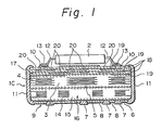
- Fig.1 shows a cross section of the embodiment of the present multilayer hybrid circuit, in which the same reference numerals as those in Figs.8A and 8B show the same members.
- the numeral 17 is an inner wiring portion mounted on a capacitor portion 5.
- the inner wiring portion 17 has at least one insulation layer 18 (three insulation layers 18 are shown in Fig.1), a flat conductive layer 19 deposited on said insulation layer 17, and a through hole 20 which penetrates through insulation layers 17 for electrically coupling said flat conductive patterns 19 on different layers.
- the conductive layers 19 and the through holes 20 are provided depending upon the desired wiring pattern of an electrical circuit.
- the inner wiring portion 17 couples also a surface pattern 10 which a pin 12 of an external component 2 is connected, with a side terminal 11 which inner passive components (an inductor, a capacitor, and/or a resistor) is connected.
- the conductive material for a through hole conductor 20, and a flat conductive layer 19 is Ag, Ag-Pd, or Pd.
- the insulation layer 18 is for instance made of ceramics, ferrite or glass.
- the inner wiring portion 17 is produced through thick film printing process, and the sintering process, as is the case of a laminated body 1C.
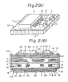
- Figs.2 and 3 show another embodiment of the present multilayer hybrid circuit, in which a laminated body 1D has a first inner wiring portion 17A on one surface of the laminated body 1D, and a second inner wiring portion 17B on the other surface of the laminated body 1D.
- a plurality of external components 2 are mounted on the first surface of the laminated body 1D.
- the first inner wiring portion 17A effects the connection not only between external components 2 and side terminals 11, but also between the external components 2 themselves.
- the second inner wiring portion 17B effects the connection between the resistor network 9 and side terminals 11.
- the inner wiring portion 17, 17A, or 17B is useful to connect not only between external components 2 and side terminals 11, but also between inductors, capacitors and/or resistors mounted in the laminated body. Further, the connection between an external component 2 and an inner component (an inductor, a capacitor, and/or a resistor) is effected by the inner wiring portion 17, without using side terminals 11.
- the layers are classified to an inner wiring portion, a capacitor portion, an inductor portion, and a resistor portion in the thickness direction of the layers.
- the latter three portions include a plurality of electronic components in each portion.
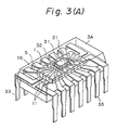
- Figs.3A and 3B show another embodiment of the multilayer hybrid circuit according to the present invention, and Fig.3A is a perspective view and Fig.3B is a cross section of Fig.3A.
- the numeral 1 shows a laminated body which is similar to that of 1C in Fig.1, and 1D in Fig.2.
- the laminated body 1 has a capacitor 5 and/or an inductor 16.
- the laminated body 1 may also include a resistor and/or an inner wiring portion.
- the capacitor 5 is produced by laminating a dielectric layer 3 and a conductive film 4, and an terminal of each capacitor is coupled with a side terminal 11 for external connection.
- An inductor 16 is produced by a ferrite layer 15 and a conductive layer 19 through thick film printing process so that conductive film 19 forms a coil. It should be appreciated that a transformer is also possible by arranging conductive layer and ferrite layer in a laminated body.
- a resistor network 9 is provided on the rear portion of the body 1.
- the resistor network 9 comprises a resistor layer 8 and a conductive layer 8B deposited on a glass layer 6 which is provided on the rear portion of the body 1.
- the resistor network 9 is covered with the glass layer 6B for protection purposes.
- the resistor network may be provided on both the surfaces of the laminated body 1, although Fig.3B shows the case that the resistor network is provided on only the rear surface of the laminated body 1.
- the numeral 50 is a pad provided on a surface of the body 1 for bonding of an IC.
- the laminated body 1, the resistor network 9, the pad 50 and the side terminal 11 are sintered at about 800 °C.
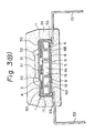
- the numeral 51 shows a conductive film which is deposited on the sintered laminated body 1, and the numeral 31 is a bare chip adhered on said conductive film 51.
- the bare chip 31 is for instance a semiconductor or an integrated circuit bare chip.
- the conductive film 51 is produced through a thick film printing process, an evaporation process, or sputtering process of metal (silver, copper, aluminium, molybudenum, gold, or palladium).
- the bare chip 31 is fixed on the laminated body through the steps of printing conductive paste on the laminated body 1 through thick film printing process, placing a bare chip 31 on said paste, and heating the body at 150-160 °C. That process provides the conductive film and the adhesion of a bare chip simultaneously.
- the numeral 32 is a conductive wire made of gold for bonding a bare chip 31 to a pad 50. It should be noted that bare chips may be mounted on both the surfaces of the laminated body 1, although Fig.3 shows the case that a bare chip is mounted on only one surface of the body 1.
- the laminated body 1 After the bare chip 31 is mounted on the laminated body 1, the laminated body 1 is placed on a lead frame so that a side terminal 11 is placed on a proper lead terminal 33 of a lead frame.
- the side terminal 11 of the laminated body 1 is conductively fixed to the lead terminal 33 of the lead frame by using conductive paste or solder 53.
- the laminated body 1 is molded by plastics 4 which covers the laminated body 1, the bare chip 31, the boding wire 32, and a part of the lead terminal 33. Finally, an outer portion (not shown) of a lead frame is removed.
- connection of the bare chip is not restricted to bonding of gold wire, but Tape Automated Bonding (TAB system) and conventional soldering are possible. Further, in some cases, the molding process by plastics may be omitted.
- TAB system Tape Automated Bonding
- Fig.4 shows another embodiment of the present invention, in which a plurality of bare chips 2 are mounted on a laminated body 1D of Fig.2B, and the whole body including the laminated body 1D and the bare chips are molded with plastics 34, and the side terminals 11 are coupled with lead terminals 33.
- a bare chip, and inner components including a capacitor, an inductor and a resistor are connected to each other through the side terminal 11, and/or an inner wiring portion.
- Figs.5A and 5B show some examples of circuit diagrams of the hybrid circuit according to the present invention, in which a bare chip 31 which is an active device, and passive devices including a capacitor 55, an inductor 56, and/or a resistor 57 enclosed by dotted line 1E are included in a single chip.
- the numeral 33 shows a lead terminal for external connection of a hybrid integrated circuit.
- a bare chip 31 is fixed on a laminated body 1 directly, or through a conductive film 51.
- the conductive film 51 functions as a heat sink.
- the coefficient of heat transfer of titanium-oxide porcelain and Barium-titanate porecelain is 0.0067w/cm ⁇ °C, and 0.0028 w/cm ⁇ °C, respectively.
- those values of silver and copper are 4.10w/cm ⁇ °C, and 3.80w/cm ⁇ °C, respectively. Therefore, the use of the conductive film 51 of silver or copper effects the dissipation of heat generated in a bare chip 31, and prevents the overheat or high temperature of a bare chip.
- the embodiments of Figs.3 and 4 have the feature that an active element by a semiconductor bare chip and a passive element by a laminated body are mounted in a single hybrid circuit chip, which is molded together. Therefore, it is not necessary to mount passive elements on a printed circuit board which mounts a semiconductor chip, and the number of components is considerably reduced. Further, no printed pattern on a printed circuit board for coupling an active element and a passive element is necessary, and therefore, the structure of a printed pattern is simplified.
- Figs.6A and 6B show another embodiment of the present invention.
- Fig.6A shows a plane view
- Fig.6B shows a cross section of the same
- Fig.6C shows the cross section of Fig.6A and shows the connection to a mother board
- Fig.6D shows a partially enlarged view of Fig.6C.
- the feature of that embodiment in Figs.6A through 6D is the use of a relay board 70 between a mother board 60 and a laminated body 1.
- the relay board 70 is made of resilient plastics board 70 and conductive patterns 73 printed on that relay board 70.
- the relay board 70 has a hole or a window which relates to a laminated body 1. Therefore, the shape of the relay board 70 is in ring-shaped.
- the conductive pattern 73 on the relay board 70 is soldered to the related conductive pattern 74 or the side terminal 11 of the laminated body 1 through the solder 13.
- the window of the relay board 70 is preferably a little smaller than the area of the laminated body 1, so that the laminated body 1 is placed on the ring-shaped relay board 70.
- the mother board 60 has a window 76 which is a little larger than the area of the relay board 70 so that the relay board 70 is positioned in that window with a small spacing (for instance that spacing is 0.2 mm).
- the conductive pattern 73 on the relay board 70 is connected to the conductive pattern 77 on the mother board 60 through the solder 13.
- the laminated body 1 is preferably fixed to the relay board 70 by using adhesive 80 so that the laminated body 1 is positioned correctly during the soldering operation.
- the height h2 between the top of a component and the surface of the mother board may be lower than that when no window is provided.
- a mother board with no window is possible if that height of a component is not problem.
- Figs.7A and 7B show the modification of the embodiment of Figs.6A through 6D.
- the feature of Figs.7A and 7B is that a laminated body 1 is fixed to a mother board 60 upside down.
- a laminated body in the embodiments of Figs.6 and 7 may be that which has an inner wiring portion, that which has no inner wiring portion, or that of Fig.3 which is molded with a semiconductor bare chip. Further, a laminated body in Figs.6 or 7 may mount semicondutor chips on both the surfaces of the same, although the drawings of Figs.6 and 7 show a laminated body which has a semiconductor chip 2 on only one surface.
Abstract
Description
- The present invention relates to an improvement of a multilayer hybrid circuit which has a laminated printed circuit board including, at least, an inductor and/or a capacitor and/or a resistor in the printed circuit board itself.
- Conventionally, electronic components are mounted on the surface of a printed circuit board, and the wiring among the components are effected through a printed wiring on the board. However, the high density mounting of electronic components requires the improvements for mounting components.
- The USP 4,322,698 provides one solution for high density mounting, and discloses a multilayer hybrid circuit which has a laminated printed circuit board which includes an inductor, a capacitor and/or a resistor. Since those components are produced in a board (not on the surface of the board), the size of the system can be miniturized, and the high density mounting has become possible.
- Fig.8A and 8B show such prior multilayer hybrid circuits. In Fig.8A, a laminated body 1A has a plurality of dielectric laminated
layers 3 and a plurality ofconductive films 4 so that thoseconductive films 4 and thosedielectric layers 3 compose a plurality ofcapacitors 5. Aglass layer 6 is attached on at least one surface of the laminated body 1A, and aresistor network 9 which has aresistor layer 8 and aconductive layer 7 is attached on saidglass layer 6. A printedwiring pattern 10 is deposited on at least one surface of the laminated body 1A, and a plurality ofterminals 11 for external connection are deposited on the sides of the laminated body 1A. Theconductive pattern 10 is used for mounting an electronic component 2 (for instance an integrated circuit, or a transistor) on the laminated body 1A. The lamainated body 1A is produced through thick film printing process, and sintering process. An externalelectronic component 2 is soldered on theconductive pattern 10 by soldering aterminal wire 12 of thecomponent 10 to theconductive pattern 10 by thesolder 13. - In the prior structure of Fig.8B, the laminated
body 1B has not only capacitors and resistors, but also inductors 16 having aninternal conductor 14 and aferrite layer 15. In producing an inductor, an U-shapedconductive pattern 14a is printed, next a ferrite pattern which is dielectric is deposited so that a window is kept at the one end of said U-shapedpattern 14a. Next, another U-shapedconductive pattern 14b is deposited on the ferrite pattern so that end of thepattern 14a at the window of the ferrite pattern is connected to the end of thesecond pattern 14b. Thus, a one turn coil is produced by a pair of U-shapedconductive patterns turns patterns - However, a prior multilayer hybrid circuit has the following disadvantages.
- (a) First, conventionally, a wiring between a surface component, and a
capacitor 5, aninductor 16, or, aresistor 9, is effected by using a surface printedconductive pattern 10 and aside terminal 11 deposited on the surface of the laminated body. However, when a complicatedexternal component 2 which has many external wiring pins is mounted on the board, thewiring pattern 10 must also be complicated. Thus, the area or the size of the board for the wiring pattern must be large, and sometimes that area required for wiring is larger than the area for mounting internal passive components. Further, a large number ofside terminals 11 must be provided, and the insulation between theside terminals 11 is difficult when theside terminals 11 are so densed. - (b) Secondly, an
external component 2 is attached on the board through conventional wiring process, and theboard 1A or 1B is mounted on a mother board bysoldering side terminals 11 to a printed pattern on the mother board. In that structure, thecomponent 2 is supported by thewire 12 of thecomponent 2 itself. However, that structure has the disadvantage that the complicatedfine surface pattern 10 on the surface of the board is difficult. - (c) Further, since the structure of a multilayer hybrid circuit is so sophiscated, it is mechanically weak, and is easily damaged. In particular, when a multilayer hybrid circuit is mounted on a conventional printed mother board, a small deformation of a printed mother board would then apply a significant amount of stress to a multilayer hybrid circuit board, and damage the same.
- (d) Because of the above disadvantages, the density of electronic components on a laminated hybrid circuit is not enough.
- It is an object, therefore, of the present invention to provide a new and improved multilayer hybrid circuit by overcoming the disadvantages and limitations of a prior multilayer hybrid circuit.
- It is also an object of the present invention to proide a multilayer hybrid circuit which mounts densed components with densed wiring.
- The above and other objects are attained by a multilayer hybrid circuit comprising an essentially flat-shaped laminated body which includes at least one selected from capacitor, inductor, resistor, and inner wiring portion; and a plurality of side terminals provided on side walls of said laminated body for external connection of said capacitor, said inductor, and said resistor; said capacitor being composed of a dielectric layer and conductive layers coupled with said side terminal; said inductor being composed of a magnetic layer and a plurality of U-shaped conductive layers composing a coil by sandwiching said magnetic layer between each U-shaped conductive layers; said resistor being composed of a dielectric layer and a resistor layer deposited on said dielectric layer together with a conductive layer for coupling said resistor layer with one of said side terminals; said inner wiring portion having at least one dielectric layer, a conductive pattern deposited on said dielectric layer, and a conductive through hole penetrating a dielectric layer for connecting conductive patterns on different dielectric layers, and said conductive pattern being coupled with said side terminals; and an electronic component mounted on said laminated body so that a wiring for said electronic component is effected through said inner wiring portion.
- Said electronic component is preferably a bare chip, and is molded by plastics with the multilayer hybrid circuit itself.
- The foregoing and other objects, features, and attendant advantages of the present invention will be appreciated as the same become better understood by means of the following description and accompanying drawings wherein;
- Fig.1 shows a cross section of a multilayer hybrid circuit according to the present invention,
- Fig.2A is a perspective view of another embodiment of a multilayer hybrid circuit according to the present invention,
- Fig.2B is a cross section of the multilayer hybrid circuit of Fig.2A,
- Fig.3A is a perspective view of still another embodiment of a multilayer hybrid circuit according to the present invention,
- Fig.3B is a cross section of Fig.3A,
- Fig.4 shows a cross section of another embodiment of the multilayer hybrid circuit according to the present invention,
- Fig.5A is an example of a circuit diagram produced in a structure of Figs.3A and 3B,
- Fig.5B is another example of a circuit diagram produced in a structure of Figs.3A and 3B,
- Fig.6A is a plane view of still another embodiment of the present invention,
- Fig.6B is a side cross section of Fig.6A,
- Fig.6C is a side cross section of Fig.6A, and shows the mounting of the multilayer hybrid circuit to a mother board,
- Fig.6D is a partially enlarged view of Fig.6C,
- Fig.7A is a cross section of still another embodiment of the present invention,
- Fig.7B is a partially enlarged view of Fig.7A,
- Fig.8A is a cross section of a prior multilayer hybrid circuit, and
- Fig.8B is a cross section of another prior multilayer hybrid circuit.
- Fig.1 shows a cross section of the embodiment of the present multilayer hybrid circuit, in which the same reference numerals as those in Figs.8A and 8B show the same members. The
numeral 17 is an inner wiring portion mounted on acapacitor portion 5. Theinner wiring portion 17 has at least one insulation layer 18 (threeinsulation layers 18 are shown in Fig.1), a flatconductive layer 19 deposited on saidinsulation layer 17, and a throughhole 20 which penetrates throughinsulation layers 17 for electrically coupling said flatconductive patterns 19 on different layers. Of course, theconductive layers 19 and the throughholes 20 are provided depending upon the desired wiring pattern of an electrical circuit. - The
inner wiring portion 17 couples also asurface pattern 10 which apin 12 of anexternal component 2 is connected, with aside terminal 11 which inner passive components (an inductor, a capacitor, and/or a resistor) is connected. The conductive material for athrough hole conductor 20, and a flatconductive layer 19 is Ag, Ag-Pd, or Pd. Theinsulation layer 18 is for instance made of ceramics, ferrite or glass. Theinner wiring portion 17 is produced through thick film printing process, and the sintering process, as is the case of a laminatedbody 1C. - Figs.2 and 3 show another embodiment of the present multilayer hybrid circuit, in which a laminated body 1D has a first
inner wiring portion 17A on one surface of the laminated body 1D, and a secondinner wiring portion 17B on the other surface of the laminated body 1D. A plurality ofexternal components 2 are mounted on the first surface of the laminated body 1D. The firstinner wiring portion 17A effects the connection not only betweenexternal components 2 andside terminals 11, but also between theexternal components 2 themselves. The secondinner wiring portion 17B effects the connection between theresistor network 9 andside terminals 11. - Further, it should be noted that further external components may be mounted on the second
inner wiring portion 17. In that case, the connection between said further comopnents and side terminals is effected by the secondinner wiring portion 17B. - It should be appreciated that the
inner wiring portion external components 2 andside terminals 11, but also between inductors, capacitors and/or resistors mounted in the laminated body. Further, the connection between anexternal component 2 and an inner component (an inductor, a capacitor, and/or a resistor) is effected by theinner wiring portion 17, without usingside terminals 11. - It should be noted that the layers are classified to an inner wiring portion, a capacitor portion, an inductor portion, and a resistor portion in the thickness direction of the layers. The latter three portions include a plurality of electronic components in each portion.
- Figs.3A and 3B show another embodiment of the multilayer hybrid circuit according to the present invention, and Fig.3A is a perspective view and Fig.3B is a cross section of Fig.3A.
- In those figures, the
numeral 1 shows a laminated body which is similar to that of 1C in Fig.1, and 1D in Fig.2. Thelaminated body 1 has acapacitor 5 and/or aninductor 16. Thelaminated body 1 may also include a resistor and/or an inner wiring portion. Thecapacitor 5 is produced by laminating adielectric layer 3 and aconductive film 4, and an terminal of each capacitor is coupled with aside terminal 11 for external connection. Aninductor 16 is produced by aferrite layer 15 and aconductive layer 19 through thick film printing process so thatconductive film 19 forms a coil. It should be appreciated that a transformer is also possible by arranging conductive layer and ferrite layer in a laminated body. - A
resistor network 9 is provided on the rear portion of thebody 1. Theresistor network 9 comprises aresistor layer 8 and aconductive layer 8B deposited on aglass layer 6 which is provided on the rear portion of thebody 1. Theresistor network 9 is covered with theglass layer 6B for protection purposes. The resistor network may be provided on both the surfaces of thelaminated body 1, although Fig.3B shows the case that the resistor network is provided on only the rear surface of thelaminated body 1. The numeral 50 is a pad provided on a surface of thebody 1 for bonding of an IC. - The
laminated body 1, theresistor network 9, thepad 50 and theside terminal 11 are sintered at about 800 °C. - The numeral 51 shows a conductive film which is deposited on the sintered
laminated body 1, and the numeral 31 is a bare chip adhered on saidconductive film 51. Thebare chip 31 is for instance a semiconductor or an integrated circuit bare chip. Theconductive film 51 is produced through a thick film printing process, an evaporation process, or sputtering process of metal (silver, copper, aluminium, molybudenum, gold, or palladium). - The
bare chip 31 is fixed on the laminated body through the steps of printing conductive paste on thelaminated body 1 through thick film printing process, placing abare chip 31 on said paste, and heating the body at 150-160 °C. That process provides the conductive film and the adhesion of a bare chip simultaneously. The numeral 32 is a conductive wire made of gold for bonding abare chip 31 to apad 50. It should be noted that bare chips may be mounted on both the surfaces of thelaminated body 1, although Fig.3 shows the case that a bare chip is mounted on only one surface of thebody 1. - After the
bare chip 31 is mounted on thelaminated body 1, thelaminated body 1 is placed on a lead frame so that aside terminal 11 is placed on aproper lead terminal 33 of a lead frame. Theside terminal 11 of thelaminated body 1 is conductively fixed to thelead terminal 33 of the lead frame by using conductive paste orsolder 53. Then, thelaminated body 1 is molded byplastics 4 which covers thelaminated body 1, thebare chip 31, the bodingwire 32, and a part of thelead terminal 33. Finally, an outer portion (not shown) of a lead frame is removed. - The connection of the bare chip is not restricted to bonding of gold wire, but Tape Automated Bonding (TAB system) and conventional soldering are possible. Further, in some cases, the molding process by plastics may be omitted.
- Fig.4 shows another embodiment of the present invention, in which a plurality of
bare chips 2 are mounted on a laminated body 1D of Fig.2B, and the whole body including the laminated body 1D and the bare chips are molded withplastics 34, and theside terminals 11 are coupled withlead terminals 33. - In the above embodiments of Figs.3 and 4, a bare chip, and inner components including a capacitor, an inductor and a resistor are connected to each other through the
side terminal 11, and/or an inner wiring portion. - Figs.5A and 5B show some examples of circuit diagrams of the hybrid circuit according to the present invention, in which a
bare chip 31 which is an active device, and passive devices including acapacitor 55, aninductor 56, and/or aresistor 57 enclosed bydotted line 1E are included in a single chip. The numeral 33 shows a lead terminal for external connection of a hybrid integrated circuit. - A
bare chip 31 is fixed on alaminated body 1 directly, or through aconductive film 51. Theconductive film 51 functions as a heat sink. The coefficient of heat transfer of titanium-oxide porcelain and Barium-titanate porecelain is 0.0067w/cm·°C, and 0.0028 w/cm·°C, respectively. On the other hand, those values of silver and copper are 4.10w/cm·°C, and 3.80w/cm·°C, respectively. Therefore, the use of theconductive film 51 of silver or copper effects the dissipation of heat generated in abare chip 31, and prevents the overheat or high temperature of a bare chip. - As described, the embodiments of Figs.3 and 4 have the feature that an active element by a semiconductor bare chip and a passive element by a laminated body are mounted in a single hybrid circuit chip, which is molded together. Therefore, it is not necessary to mount passive elements on a printed circuit board which mounts a semiconductor chip, and the number of components is considerably reduced. Further, no printed pattern on a printed circuit board for coupling an active element and a passive element is necessary, and therefore, the structure of a printed pattern is simplified.
- Figs.6A and 6B show another embodiment of the present invention. Fig.6A shows a plane view, Fig.6B shows a cross section of the same, Fig.6C shows the cross section of Fig.6A and shows the connection to a mother board, and Fig.6D shows a partially enlarged view of Fig.6C. The feature of that embodiment in Figs.6A through 6D is the use of a
relay board 70 between amother board 60 and alaminated body 1. Therelay board 70 is made ofresilient plastics board 70 andconductive patterns 73 printed on thatrelay board 70. - The
relay board 70 has a hole or a window which relates to alaminated body 1. Therefore, the shape of therelay board 70 is in ring-shaped. Theconductive pattern 73 on therelay board 70 is soldered to the relatedconductive pattern 74 or theside terminal 11 of thelaminated body 1 through thesolder 13. The window of therelay board 70 is preferably a little smaller than the area of thelaminated body 1, so that thelaminated body 1 is placed on the ring-shapedrelay board 70. - The
mother board 60 has awindow 76 which is a little larger than the area of therelay board 70 so that therelay board 70 is positioned in that window with a small spacing (for instance that spacing is 0.2 mm). Theconductive pattern 73 on therelay board 70 is connected to theconductive pattern 77 on themother board 60 through thesolder 13. Thelaminated body 1 is preferably fixed to therelay board 70 by using adhesive 80 so that thelaminated body 1 is positioned correctly during the soldering operation. - When a
laminated body 1 is mounted on a mother board through a relay board which is resilient, even if a stress is applied to a mother board, said stress is absorbed by the resilient relay board, and no stress is applied to thelaminated body 1, and further, no excessive stress is applied to the solder and therefore the connection by solder is not damaged. - Because of the presence of a
window 76 of a mother board, the height h2 between the top of a component and the surface of the mother board may be lower than that when no window is provided. Of course, a mother board with no window is possible if that height of a component is not problem. - Figs.7A and 7B show the modification of the embodiment of Figs.6A through 6D. The feature of Figs.7A and 7B is that a
laminated body 1 is fixed to amother board 60 upside down. - A laminated body in the embodiments of Figs.6 and 7 may be that which has an inner wiring portion, that which has no inner wiring portion, or that of Fig.3 which is molded with a semiconductor bare chip. Further, a laminated body in Figs.6 or 7 may mount semicondutor chips on both the surfaces of the same, although the drawings of Figs.6 and 7 show a laminated body which has a
semiconductor chip 2 on only one surface. - From the foregoing it will now be apparent that a new and improved multilayer hybrid circuit has been found. It should be understood of course that the embodiments disclosed are merely illustrative and are not intended to limit the scope of the invention. Reference should be made to the appended claims, therefore, rather than the specification as indicating the scope of the invention.
Claims (10)
- (1) A multilayer hybrid circuit comprising an essentially flat-shaped laminated body which includes at least one selected from capacitor, inductor, resistor, and inner wiring portion; and a plurality of side terminals provided on side walls of said laminated body for external connection of said capacitor, said inductor, and said resistor,
said capacitor being composed of a dielectric layer and conductive layers coupled with said side terminal,
said inductor being composed of a magnetic layer and a plurality of U-shaped conductive layers composing a coil by sandwiching said magnetic layer between each U-shaped conductive layers,
said resistor being composed of a dielectric layer and a resistor layer deposited on said dielectric layer together with a conductive layer for coupling said resistor layer with one of said side terminals,
said inner wiring portion having at least one dielectric layer, a conductive pattern deposited on said dielectric layer, and a conductive through hole penetrating a dielectric layer for connecting conductive patterns on different dielectric layers, and said conductive pattern being coupled with said side terminals, and
an electronic component being mounted on said laminated body. - (2) A multilayer hybrid circuit according to claim 1, wherein said electronic component is a bare semiconductor chip mounted on said laminated body, and molded by plastics with said laminated body, and a bulk molded body has a plurality of conductive pins for external connection.
- (3) A multilayer hybrid circuit according to claim 2, wherein a conductive layer is provided between said bare semiconductor chip and said laminated body so that said conductive layer functions as a heat sink.
- (4) A multilayer hybrid circuit according to claim 2, wherein said terminal pin is offset to L-shaped.
- (5) A laminated hybrid circuit according to claim 1, further comprising a resilient relay board which has a conductive pattern and carries said laminated body so that said laminated body is mounted on a mother board through said relay board, and is electrically coupled with the mother board through said conductive pattern on the relay board.
- (6) A multilayer hybrid circuit comprising an essentially flat-shaped laminated body which includes at least one selected from a capacitor portion, an inductor portion, a resistor portion and an inner wiring portion laminated to each other, and a plurality of side terminals provided on side walls of said laminated body for external connection of a capacitor, an inductor, and a resistor,
said capacitor portion being composed of a dielectric layer and conductive layers coupled with said side terminals for providing capacitance between conductive layers,
said inductor portion being composed of a magnetic layer and a plurality of U-shaped conductive layers composing a coil by sandwiching said magnetic layer between each U-shaped conductive layers,
said resistor portion being composed of a dielectric layer and a resistor layer deposited on said dielectric layer together with a conductive layer for coupling said resistor layer with one of said side terminals,
said inner wiring poriton being composed of at least one dielectric layer, a conductive pattern deposited on said dielectric layer, and a conductive through hole for connecting electrically conductive patterns on different dielectric layers, and said conductive pattern is coupled with said side terminals,
an electronic component in bare chip form being mounted on said laminated body so that a wiring for said electronic component is effected through said inner wiring portion,
a plurality of L-shaped terminal pins for external connection coupled with each side terminal, and
said electronic component and said laminated body being molded together by plastics. - (7) A multilayer hybrid circuit according to claim (6), wherein a conductive layer is provided between said bare electronic component chip and said laminated body so that said conductive layer functions as a heat sink.
- (8) A multilayer hybrid circuit according to claim 6, further comprising a resilient relay board which has a conductive pattern and carries said multilayer hybrid circuit so that said multilayer hybrid circuit is mounted on a mother board through said relay board.
- (9) A multilayer hybrid circuit according to claim 8, wherein said relay board is ring-shaped having a center hole.
- (10) A multilayer hybrid circuit according to claim 5, wherein said relay board is ring-shaped having a center hole.
Priority Applications (1)
| Application Number | Priority Date | Filing Date | Title |
|---|---|---|---|
| EP97200966A EP0789390B1 (en) | 1989-01-14 | 1990-01-12 | A method for producing a multilayer hybrid circuit |
Applications Claiming Priority (2)
| Application Number | Priority Date | Filing Date | Title |
|---|---|---|---|
| JP7378/89 | 1989-01-14 | ||
| JP1007378A JP2790640B2 (en) | 1989-01-14 | 1989-01-14 | Structure of hybrid integrated circuit components |
Related Child Applications (1)
| Application Number | Title | Priority Date | Filing Date |
|---|---|---|---|
| EP97200966A Division EP0789390B1 (en) | 1989-01-14 | 1990-01-12 | A method for producing a multilayer hybrid circuit |
Publications (2)
| Publication Number | Publication Date |
|---|---|
| EP0379404A2 true EP0379404A2 (en) | 1990-07-25 |
| EP0379404A3 EP0379404A3 (en) | 1993-03-31 |
Family
ID=11664289
Family Applications (2)
| Application Number | Title | Priority Date | Filing Date |
|---|---|---|---|
| EP97200966A Expired - Lifetime EP0789390B1 (en) | 1989-01-14 | 1990-01-12 | A method for producing a multilayer hybrid circuit |
| EP19900400092 Withdrawn EP0379404A3 (en) | 1989-01-14 | 1990-01-12 | A multilayer hybrid circuit |
Family Applications Before (1)
| Application Number | Title | Priority Date | Filing Date |
|---|---|---|---|
| EP97200966A Expired - Lifetime EP0789390B1 (en) | 1989-01-14 | 1990-01-12 | A method for producing a multilayer hybrid circuit |
Country Status (3)
| Country | Link |
|---|---|
| EP (2) | EP0789390B1 (en) |
| JP (1) | JP2790640B2 (en) |
| DE (1) | DE69034095T2 (en) |
Cited By (11)
| Publication number | Priority date | Publication date | Assignee | Title |
|---|---|---|---|---|
| EP0433176A2 (en) * | 1989-12-15 | 1991-06-19 | TDK Corporation | A multilayer hybrid circuit |
| EP0562629A2 (en) * | 1992-03-26 | 1993-09-29 | Sumitomo Electric Industries, Limited | Semiconductor device comprising a package |
| US5475262A (en) * | 1992-08-07 | 1995-12-12 | Fujitsu Limited | Functional substrates for packaging semiconductor chips |
| EP0720232A1 (en) * | 1993-09-14 | 1996-07-03 | Kabushiki Kaisha Toshiba | Multi-chip module |
| EP0851439A1 (en) * | 1996-12-26 | 1998-07-01 | Citizen Electronics Co., Ltd. | Modular surface mount circuit device and a manufacturing method thereof |
| US5777383A (en) * | 1996-05-09 | 1998-07-07 | Lsi Logic Corporation | Semiconductor chip package with interconnect layers and routing and testing methods |
| US5889445A (en) * | 1997-07-22 | 1999-03-30 | Avx Corporation | Multilayer ceramic RC device |
| US5959846A (en) * | 1996-12-26 | 1999-09-28 | Citizen Electronics, Co., Ltd. | Modular surface mount circuit device and a manufacturing method thereof |
| US6525628B1 (en) | 1999-06-18 | 2003-02-25 | Avx Corporation | Surface mount RC array with narrow tab portions on each of the electrode plates |
| EP1365451A1 (en) * | 2001-10-15 | 2003-11-26 | Matsushita Electric Industrial Co., Ltd. | Module component |
| CN109427728A (en) * | 2017-08-30 | 2019-03-05 | 日月光半导体制造股份有限公司 | Integrated-type passive block and its manufacturing method |
Families Citing this family (11)
| Publication number | Priority date | Publication date | Assignee | Title |
|---|---|---|---|---|
| DE19903456A1 (en) * | 1999-01-28 | 2000-08-10 | Philips Corp Intellectual Pty | Multi-component component |
| US6212078B1 (en) * | 1999-10-27 | 2001-04-03 | Microcoating Technologies | Nanolaminated thin film circuitry materials |
| JP4529262B2 (en) * | 2000-09-14 | 2010-08-25 | ソニー株式会社 | High frequency module device and manufacturing method thereof |
| EP1610384A3 (en) | 2004-06-14 | 2008-11-19 | Denso Corporation | Electronic unit with a substrate where an electronic circuit is fabricated |
| WO2007052528A1 (en) * | 2005-11-01 | 2007-05-10 | Kabushiki Kaisha Toshiba | Flat magnetic element and power ic package using the same |
| JP5614286B2 (en) | 2009-01-28 | 2014-10-29 | 日立金属株式会社 | Semiconductor device and power supply circuit |
| US8428286B2 (en) | 2009-11-30 | 2013-04-23 | Infineon Technologies Ag | MEMS microphone packaging and MEMS microphone module |
| US9070642B2 (en) | 2011-09-14 | 2015-06-30 | Infineon Technologies Ag | Electronic module |
| FR2983294B1 (en) | 2011-11-28 | 2014-07-11 | Schneider Electric Ind Sas | METHOD FOR EVALUATING THE MECHANICAL PERFORMANCE OF A CUTTING DEVICE AND CUTTING DEVICE FOR CARRYING OUT SAID METHOD |
| FR2983293B1 (en) | 2011-11-28 | 2014-08-01 | Schneider Electric Ind Sas | METHOD FOR EVALUATING THE MECHANICAL PERFORMANCE OF A CUTTING APPARATUS AND CUTTING APPARATUS FOR CARRYING OUT SAID METHOD |
| JPWO2015182114A1 (en) * | 2014-05-30 | 2017-04-20 | パナソニックIpマネジメント株式会社 | Semiconductor device, built-in capacitor unit, semiconductor mounting body, and method for manufacturing built-in capacitor unit |
Citations (3)
| Publication number | Priority date | Publication date | Assignee | Title |
|---|---|---|---|---|
| FR2514562A1 (en) * | 1981-10-09 | 1983-04-15 | Thomson Csf | Multilayer hybrid capacitor circuit and internal connections - has dielectric block with interconnections via pierced metallised holes to provide internal connection between layers |
| US4413308A (en) * | 1981-08-31 | 1983-11-01 | Bell Telephone Laboratories, Incorporated | Printed wiring board construction |
| FR2563656A1 (en) * | 1984-04-27 | 1985-10-31 | Nec Corp | LARGE-SCALE INTEGRATION CIRCUIT BLOCK |
Family Cites Families (9)
| Publication number | Priority date | Publication date | Assignee | Title |
|---|---|---|---|---|
| GB2045540B (en) * | 1978-12-28 | 1983-08-03 | Tdk Electronics Co Ltd | Electrical inductive device |
| JPS5818952A (en) * | 1981-07-27 | 1983-02-03 | Tdk Corp | Manufacture of hybrid integrated circuit |
| JPS5968959A (en) * | 1982-10-13 | 1984-04-19 | Tdk Corp | Formation of electronic circuit |
| DE3382208D1 (en) * | 1982-12-15 | 1991-04-18 | Nec Corp | MONOLITHIC MULTILAYER CERAMIC SUBSTRATE WITH AT LEAST ONE DIELECTRIC LAYER MADE OF A MATERIAL WITH PEROVSKIT STRUCTURE. |
| JPS59178768A (en) * | 1983-03-30 | 1984-10-11 | Tdk Corp | Composite component parts |
| JPS6127655A (en) * | 1984-07-18 | 1986-02-07 | Kazuyoshi Sone | Manufacture of integrated circuit |
| JPS6132785U (en) * | 1984-07-27 | 1986-02-27 | ティーディーケイ株式会社 | Stacked hybrid integrated DC/DC converter |
| JPS61125156A (en) * | 1984-11-22 | 1986-06-12 | Nec Corp | Semiconductor device |
| DE3888582T2 (en) * | 1987-07-01 | 1994-10-13 | Tdk Corp | Sintered ferrite body, chip inductance and composite LC part. |
-
1989
- 1989-01-14 JP JP1007378A patent/JP2790640B2/en not_active Expired - Fee Related
-
1990
- 1990-01-12 EP EP97200966A patent/EP0789390B1/en not_active Expired - Lifetime
- 1990-01-12 EP EP19900400092 patent/EP0379404A3/en not_active Withdrawn
- 1990-01-12 DE DE69034095T patent/DE69034095T2/en not_active Expired - Fee Related
Patent Citations (3)
| Publication number | Priority date | Publication date | Assignee | Title |
|---|---|---|---|---|
| US4413308A (en) * | 1981-08-31 | 1983-11-01 | Bell Telephone Laboratories, Incorporated | Printed wiring board construction |
| FR2514562A1 (en) * | 1981-10-09 | 1983-04-15 | Thomson Csf | Multilayer hybrid capacitor circuit and internal connections - has dielectric block with interconnections via pierced metallised holes to provide internal connection between layers |
| FR2563656A1 (en) * | 1984-04-27 | 1985-10-31 | Nec Corp | LARGE-SCALE INTEGRATION CIRCUIT BLOCK |
Non-Patent Citations (8)
| Title |
|---|
| PATENT ABSTRACTS OF JAPAN, vol. 011, no. 148 (E-506) 14 May 1987; & JP-A-61 285 739 (SUMITOMO ELECTRIC IND LTD) 16-12-1986 * |
| PATENT ABSTRACTS OF JAPAN, vol. 011, no. 257 (E-534) 20 August 1987; & JP-A-62 067 829 (SHARP CORP.) 27-03-1987 * |
| PATENT ABSTRACTS OF JAPAN, vol. 011, no. 309 (E-547) 08 October 1987; & JP-A-62 101 064 (SUMITOMO ELECTRIC IND LTD) 11-05-1987 * |
| PATENT ABSTRACTS OF JAPAN, vol. 012, no. 362 (E-663) 28 September 1988; & JP-A-63 117 438 (TOSHIBA CORP.) 21-05-1988 * |
| PATENT ABSTRACTS OF JAPAN, vol. 013, no. 343 (E-796) 02 August 1989; & JP-A-01 101 656 (TDK CORP.) 19-04-1989 * |
| PATENT ABSTRACTS OF JAPAN, vol. 013, no. 437 (E-826) 29 September 1989; & JP-A-01 165 216 (TDK CORP.) 29-06-1989 * |
| PATENT ABSTRACTS OF JAPAN, vol. 014, no. 139 (E-0903) 15 March 1990; & JP-A-02 003 263 (NEC CORP.) 08-01-1990 * |
| PROCEEDINGS OF THE ELECTRONIC COMPONENTS CONFERENCE, 4TH - 11TH MAY 1988 LOS ANGELES, US; pages 436 - 444; A. WEINBERG ET AL.: "VERTICALLY-INTEGRATED PACKAGE". * |
Cited By (17)
| Publication number | Priority date | Publication date | Assignee | Title |
|---|---|---|---|---|
| EP0433176A2 (en) * | 1989-12-15 | 1991-06-19 | TDK Corporation | A multilayer hybrid circuit |
| EP0433176B1 (en) * | 1989-12-15 | 2002-08-14 | TDK Corporation | A multilayer hybrid circuit |
| EP0562629A2 (en) * | 1992-03-26 | 1993-09-29 | Sumitomo Electric Industries, Limited | Semiconductor device comprising a package |
| EP0562629A3 (en) * | 1992-03-26 | 1994-03-09 | Sumitomo Electric Industries | |
| US5475262A (en) * | 1992-08-07 | 1995-12-12 | Fujitsu Limited | Functional substrates for packaging semiconductor chips |
| EP0582315B1 (en) * | 1992-08-07 | 1998-05-27 | Fujitsu Limited | Multi-chip module and process of forming it |
| EP0720232A1 (en) * | 1993-09-14 | 1996-07-03 | Kabushiki Kaisha Toshiba | Multi-chip module |
| EP0720232A4 (en) * | 1993-09-14 | 1996-11-13 | Toshiba Kk | Multi-chip module |
| US5777383A (en) * | 1996-05-09 | 1998-07-07 | Lsi Logic Corporation | Semiconductor chip package with interconnect layers and routing and testing methods |
| US5959846A (en) * | 1996-12-26 | 1999-09-28 | Citizen Electronics, Co., Ltd. | Modular surface mount circuit device and a manufacturing method thereof |
| EP0851439A1 (en) * | 1996-12-26 | 1998-07-01 | Citizen Electronics Co., Ltd. | Modular surface mount circuit device and a manufacturing method thereof |
| US5889445A (en) * | 1997-07-22 | 1999-03-30 | Avx Corporation | Multilayer ceramic RC device |
| US6525628B1 (en) | 1999-06-18 | 2003-02-25 | Avx Corporation | Surface mount RC array with narrow tab portions on each of the electrode plates |
| EP1365451A1 (en) * | 2001-10-15 | 2003-11-26 | Matsushita Electric Industrial Co., Ltd. | Module component |
| EP1365451A4 (en) * | 2001-10-15 | 2010-06-23 | Panasonic Corp | Module component |
| CN109427728A (en) * | 2017-08-30 | 2019-03-05 | 日月光半导体制造股份有限公司 | Integrated-type passive block and its manufacturing method |
| CN109427728B (en) * | 2017-08-30 | 2022-06-21 | 日月光半导体制造股份有限公司 | Integrated passive module and method for manufacturing the same |
Also Published As
| Publication number | Publication date |
|---|---|
| JPH02187054A (en) | 1990-07-23 |
| EP0789390A3 (en) | 1998-01-14 |
| DE69034095D1 (en) | 2003-09-18 |
| EP0379404A3 (en) | 1993-03-31 |
| DE69034095T2 (en) | 2004-03-25 |
| EP0789390B1 (en) | 2003-08-13 |
| EP0789390A2 (en) | 1997-08-13 |
| JP2790640B2 (en) | 1998-08-27 |
Similar Documents
| Publication | Publication Date | Title |
|---|---|---|
| US5428885A (en) | Method of making a multilayer hybrid circuit | |
| EP0789390B1 (en) | A method for producing a multilayer hybrid circuit | |
| US5519176A (en) | Substrate and ceramic package | |
| EP0720232B1 (en) | Multi-chip module | |
| US7557307B2 (en) | Electronic component and its manufacturing method | |
| US4982311A (en) | Package for very large scale integrated circuit | |
| JP2779620B2 (en) | Method for housing cage of semiconductor device and integrated circuit inside plastic package | |
| JP3201681B2 (en) | Surface mounted hybrid integrated circuit device | |
| JPH03156905A (en) | Electronic component using stacked capacitor | |
| JP2001345559A (en) | Wiring board and its manufacturing method | |
| JP2780424B2 (en) | Hybrid integrated circuit | |
| JPS60171754A (en) | Semiconductor chip carrier provided with circuit element | |
| JP2722451B2 (en) | Semiconductor device | |
| JP2002359340A (en) | Multilayer circuit board | |
| JP2571389B2 (en) | Stacked hybrid integrated circuit components | |
| JP2003078103A (en) | Circuit board | |
| JPH10173083A (en) | Wiring board for mounting electronic component and its manufacturing method | |
| JPH0722730A (en) | Composite electronic component | |
| JP4292860B2 (en) | Multilayer electronic circuit device and manufacturing method thereof | |
| TWI261902B (en) | Chip with embedded passive components and method of manufacturing the same proposed | |
| JPH042478Y2 (en) | ||
| JPH03136396A (en) | Electronic circuit component, manufacture thereof and electronic circuit apparatus | |
| JPH05326814A (en) | Lead frame for mounting electronic circuit device | |
| JPH05226518A (en) | Hybrid integrated circuit device | |
| JPS61111516A (en) | Thick film hybrid electronic component |
Legal Events
| Date | Code | Title | Description |
|---|---|---|---|
| PUAI | Public reference made under article 153(3) epc to a published international application that has entered the european phase |
Free format text: ORIGINAL CODE: 0009012 |
|
| AK | Designated contracting states |
Kind code of ref document: A2 Designated state(s): DE FR GB NL |
|
| PUAL | Search report despatched |
Free format text: ORIGINAL CODE: 0009013 |
|
| AK | Designated contracting states |
Kind code of ref document: A3 Designated state(s): DE FR GB NL |
|
| 17P | Request for examination filed |
Effective date: 19930910 |
|
| 17Q | First examination report despatched |
Effective date: 19940803 |
|
| STAA | Information on the status of an ep patent application or granted ep patent |
Free format text: STATUS: THE APPLICATION IS DEEMED TO BE WITHDRAWN |
|
| 18D | Application deemed to be withdrawn |
Effective date: 19980602 |