EP0380854A2 - Instruction buffer system for a digital computer - Google Patents
Instruction buffer system for a digital computer Download PDFInfo
- Publication number
- EP0380854A2 EP0380854A2 EP89309274A EP89309274A EP0380854A2 EP 0380854 A2 EP0380854 A2 EP 0380854A2 EP 89309274 A EP89309274 A EP 89309274A EP 89309274 A EP89309274 A EP 89309274A EP 0380854 A2 EP0380854 A2 EP 0380854A2
- Authority
- EP
- European Patent Office
- Prior art keywords
- instruction
- bytes
- buffer
- prefetch
- instruction stream
- Prior art date
- Legal status (The legal status is an assumption and is not a legal conclusion. Google has not performed a legal analysis and makes no representation as to the accuracy of the status listed.)
- Granted
Links
Images


Classifications
-
- G—PHYSICS
- G06—COMPUTING; CALCULATING OR COUNTING
- G06F—ELECTRIC DIGITAL DATA PROCESSING
- G06F9/00—Arrangements for program control, e.g. control units
- G06F9/06—Arrangements for program control, e.g. control units using stored programs, i.e. using an internal store of processing equipment to receive or retain programs
- G06F9/30—Arrangements for executing machine instructions, e.g. instruction decode
- G06F9/30145—Instruction analysis, e.g. decoding, instruction word fields
- G06F9/30149—Instruction analysis, e.g. decoding, instruction word fields of variable length instructions
-
- G—PHYSICS
- G06—COMPUTING; CALCULATING OR COUNTING
- G06F—ELECTRIC DIGITAL DATA PROCESSING
- G06F9/00—Arrangements for program control, e.g. control units
- G06F9/06—Arrangements for program control, e.g. control units using stored programs, i.e. using an internal store of processing equipment to receive or retain programs
- G06F9/30—Arrangements for executing machine instructions, e.g. instruction decode
- G06F9/38—Concurrent instruction execution, e.g. pipeline, look ahead
- G06F9/3802—Instruction prefetching
- G06F9/3816—Instruction alignment, e.g. cache line crossing
Definitions
- This invention relates generally to an instruction buffer system and to a virtual instruction cache (VIC) of a high-speed digital computer.
- VIP virtual instruction cache
- VAX 8600 computer manufactured and sold by Digital Equipment Corporation, 111 Powdermill Road, Maynard MA 97154-1418.
- the instruction pipeline for the VAX 8600 is described in T. Fossum et al. "An overview of the VAX 8600 System", Digital Technical Journal , No. 1, August 1985, pp. 8-23. Separate pipeline stages are provided for instruction fetch, instruction decode, operand address generation, operand fetch, instruction execute, and result store.
- the instruction set employed in some computers is of the variable length type, thereby forcing the instruction buffer to have added complexity.
- the instruction buffer does not "know" how many of the subsequent bytes of the instruction stream belong with the current instruction. Therefore, the instruction buffer can only respond by loading a preselected number of bytes of the instruction stream, which may or may not include an entire instruction.
- the instruction decoder will only consume those bytes associated with the immediate instruction. Thereafter, the instruction buffer must determine how many of the present bytes were used by the decoder, shift the unused bytes into the lowest order locations, and then fill the empty buffer locations with subsequent bytes of the instruction stream.
- references to the main memory to retrieve these subsequent bytes of instruction stream necessarily involves multiple clock cycles.
- many digital computers include a high speed cache between the processing unit and the main memory. Access to this cache takes only a small number of cycles of the processor's clock but often involves translating virtual addresses to physical addresses.
- some systems dedicate a cache solely to store the instructions. The access to this "instruction cache” often does not entail translating from virtual to physical addresses as the instructions are stored under their virtual addresses. This access to the instruction stream in a high speed virtual instruction cache may only involve one cycle of the processor's clock.
- each reference to the virtual instruction cache involves comparing the requested address with the desired address to first determine if the desired instruction stream is present and then retrieving the requested instruction stream. Therefore, owing to the variable length nature of the instruction set, the instruction buffer cannot predict whether a reference to the VIC will be required by the instruction currently being decoded.
- a prefetch buffer is provided to maintain a preselected number of the subsequent bytes of instruction stream which are expected to be used by the instruction decoder. This process forestalls the inevitable reference to the virtual instruction cache.
- an instruction buffer includes first and second prefetch buffers for storing a preselected number of subsequent bytes of instruction stream.
- the first prefetch buffer is independently addressable to retrieve a selected number of sequential bytes contained therein.
- Means are provided for refilling the decoder with the number of sequential bytes of instruction stream corresponding to the number of bytes currently being decoded.
- the refill means retrieves the instruction stream bytes from the first prefetch buffer sequentially and sets a "valid bit" corresponding to each byte of instruction stream retrieved.
- the second instruction buffer need only contain all valid or all invalid bytes, and therefore only one valid bit need be held for the second instruction buffer.
- the first prefetch buffer is refilled with the preselected number of subsequent instruction stream bytes in response to all of the valid bits corresponding to each byte of the instruction stream contained therein being clear.
- the second prefetch buffer is refilled with the preselected number of subsequent instruction stream bytes when it becomes empty.
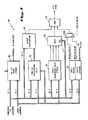
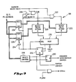
- FIGURE 1 is a top level block diagram of a portion of a pipelined computer system 10.
- the system 10 includes at least one central processing unit (CPU) 12 having access to main memory 14. It should be understood that additional CPUs could be used in such a system by sharing the main memory 14.
- CPU central processing unit
- the data path through the pipeline includes a respective set of registers for transferring the results of each pipeline stage to the next pipeline stage. These transfer registers are clocked in response to a common system clock. For example, during a first clock cycle, the first instruction is fetched by hardware dedicated to instruction fetch. During the second clock cycle, the fetched instruction is transferred and decoded by instruction decode hardware, but, at the same time, the next instruction is fetched by the instruction fetch hardware. During the third clock cycle, each instruction is shifted to the next stage of the pipeline and a new instruction is fetched. Thus, after the pipeline is filled, an instruction will be completely executed at the end of each clock cycle.
- This process is analogous to an assembly line in a manufacturing environment.
- Each worker is dedicated to performing a single task on every product that passes through his or her work stage. As each task is performed the product comes closer to completion. At the final stage, each time the worker performs his or her assigned task a completed product rolls off the assembly line.
- each CPU 12 is partitioned into at least three functional units: the memory access unit 16, the instruction unit 18, and the execution unit 20.
- the memory access unit 16 includes a main cache 22 which, on an average basis, enables the instruction and execution units 18, 20 to process data at a faster rate than the access time of the main memory 14.
- This cache 22 includes means for storing selected predefined blocks of data elements, means for receiving requests from the instruction unit 18 via a translation buffer 24 to access a specified data element, means for checking whether the data element is in a block stored in the cache 22, and means operative when data for the block including the specified data element is not so stored for reading the specified block of data in the cache 22.
- the cache provides a "window" into the main memory, and contains data likely to be needed by the instruction and execution units 18, 20.
- the organization and operation of a similar cache and translation buffer are further described in Chapter 11 of Levy and Eckhouse, Jr., Computer Programming and Architecture, The VAX-11 , Digital Equipment Corporation, pp. 351-368 (1980).
- the main memory 14 can have a proportionally slower access time than the cache 22 without substantially degrading the average performance of the computer system 10. Therefore, the main memory 14 is constructed of slower and less expensive memory elements.
- the translation buffer 24 is a high speed associative memory which stores the most recently used virtual-to-physical address translations. In a virtual memory system, a reference to a single virtual address can cause several memory references before the desired information is made available. However, where the translation buffer 24 is used, translation is reduced to simply finding a "hit" in the translation buffer 24.
- the instruction unit 18 includes a program counter 26 and a virtual instruction cache (VIC) 28 for fetching instructions from the main cache 22.
- the program counter 26 preferably addresses virtual memory locations rather than the physical memory locations of the main memory 14 and the cache 22. Thus, the virtual address of the program counter 26 must be translated into the physical address of the main memory 14 before instructions can be retrieved. Accordingly, the contents of the program counter 26 are transferred to the memory access unit 16 where the translation buffer 24 performs the address conversion.
- the instruction is retrieved from its physical memory location in the cache 22 using the converted address.
- the cache 22 delivers the instruction over data return lines to the VIC 28.
- the VIC 28 contains prestored instructions at the addresses specified by the program counter 26, and the addressed instructions are available immediately for the transfer into an instruction buffer (IBUFFER) 30. From the buffer 30, the addressed instructions are fed to an instruction decoder 32 which decodes both the opcodes and the specifiers. An operand processing unit (OPU) 34 fetches the specified operands and supplies them to the execution unit 20.
- IBUFFER instruction buffer
- OPU operand processing unit
- the OPU 34 also produces virtual addresses.
- the OPU 34 produces virtual addresses for memory source (read and destination (write) operands.
- the OPU 34 delivers these virtual addresses to the memory access unit 16 where they are translated to physical addresses.
- the physical memory locations of the cache 22 are then accessed to fetch the operands for the memory source operands.
- the first byte contains the opcode, and the following bytes are the operand specifiers to be decoded.
- the first byte of each specifier indicates the addressing mode for that specifier. This byte is usually broken in halves, with one-half specifying the addressing mode and the other half specifying a register to be used for addressing.
- the instructions preferably have a variable length, and various types of specifiers can be used with the same opcode, as disclosed in Strecker et al., U.S. Patent 4,241,397 issued December 23, 1980.
- the first step in processing the instructions is to decode the opcode portion of the instruction.
- the first portion of each instruction consists of its opcode which specifies the operation to be performed in the instruction, and the number and type of specifiers to be used. Decoding is accomplished using a table-look-up technique in the instruction decoder 32. Later, the execution unit 20 performs the specified operation by executing prestored microcode, beginning at a predetermined starting address for the specified operation. Also, the decoder 32 determines where source-operand and destination-operand specifiers occur in the instruction and passes these specifiers to the OPU 34 for preprocessing prior to execution of the instruction.
- a preferred instruction decoder for use with the refill method and apparatus of the present invention is described in the above referenced D. Fite et al. U.S. patent application Serial No. , filed , and entitled "Decoding Multiple Specifiers in a Variable Length Instruction Architecture," incorporated herein by reference.
- the OPU 34 parses the operand specifiers and computes their effective addresses; this process involves reading GPRS and possibly modifying the GPR contents by autoincrementing or autodecrementing.
- the operands are then fetched from those effective addresses and passed on to the execution unit 20, which executes the instruction and writes the result into the destination identified by the destination pointer for that instruction.
- a set of queues 36 includes a fork queue for storing the microcode dispatch address, a source pointer queue for storing the source-operand locations, and a destination pointer queue for storing the destination location. Each of these queues is a FIFO buffer capable of holding the data for multiple instructions.
- the execution unit 20 also includes a source list 38, which is a multi-ported register file containing a copy of the GPRS and a list of source operands. Thus, entries in the source pointer queue will either point to GPR locations for register operands, or point to the source list for memory and literal operands. Both the memory access unit 16 and the instruction unit 18 write entries in the source list 38, and the execution unit 20 reads operands out of the source list 38 as needed to execute the instructions.
- the execution unit 20 includes an instruction issue unit 40, a microcode execution unit 42, an arithmetic and logic unit (ALU) 44, and a retire unit 46.
- ALU arithmetic and logic unit
- the processor's instruction fetch hardware may be fetching one instruction while other hardware is decoding the operation code of a second instruction, fetching the operands of a third instruction, executing a fourth instruction, and storing the processed data of a fifth instruction.
- FIG. 2 illustrates a pipeline for a typical instruction such as: ADDL3 R0,B ⁇ 12(R1),R2 This is a long-word addition using the displacement mode of addressing.
- the program count (PC) of the instruction is created; this is usually accomplished either by incrementing the program counter 26 from the previous instruction, or by using the target address of a branch instruction.
- the PC is then used to access VIC 28 in the second stage of the pipeline.
- the instruction data is available from the cache 22 for use by the instruction decoder 32, or to be loaded into the IBUFFER 30.
- the instruction decoder 32 decodes the opcode and the three specifiers in a single cycle, as will be described in more detail below.
- the R0 and R2 numbers are passed to the ALU 44, and the R1 number along with the byte displacement is sent to the OPU 34 at the end of the decode cycle.
- stage four the OPU 34 reads the contents of its GPR register file at location R1, adds that value to the specified displacement (12), and sends the resulting address to the translation buffer 24 in the memory access unit 16, along with an OP READ request, at the end of the address generation stage.
- stage five the memory access unit 16 selects the address generated in stage four for execution. Using the translation buffer 24, the memory access unit 16 translates the virtual address to a physical address during the address translation stage. The physical address is then used to address the cache 22, which is read in stage six of the pipeline.
- stage seven of the pipeline the instruction is issued to the ALU 44 which adds the two operands and sends the result to the retire unit 46.
- the register numbers for R1 and R2, and a pointer to the source list location for the memory data are sent to the execution unit and stored in the pointer queues.
- the execution unit looks for the two source operands in the source list. In this particular example, it finds only the register data R0, but at the end of this stage the memory data arrives and is substituted for the invalidated read-out of the register file. Thus, both operands are available in the instruction execution stage.
- the result data is paired with the next entry in the retire queue. Although several functional execution units can be busy at the same time, only one instruction is retired in a single cycle.
- the data is written into the GPR portion of the register files in both the execution unit 20 and the instruction unit 18.
- the VIC 28 is constructed of four groups of self-timed rams (STRAMS), and acts as a window into the main memory 14.
- STRAMS self-timed rams
- the first group of VIC STRAMS is the data stram 50 which provides storage space for the actual instruction stream (ISTREAM) retrieved from the main cache 22.
- the data stram 50 contains 1024 storage locations, with each storage location being 64-bits in width. From the size of the data stram 50, it should be apparent that the ISTREAM is retrieved in quadword (8-byte) packets. Accordingly, the data path between the main cache 22 and the VIC 28 is also 64-bits in width and a quadword of ISTREAM can be transferred during each system clock cycle.
- a set of tag strams 52 is provided.
- the tag strams 52 store the upper nineteen bits 31:13 of the quadword address.
- ISTREAM is retrieved from the main cache 22 in four quadword blocks.
- a request to the main cache 22 for the first quadword in a block causes the main cache 22 to also return the three following quadwords.
- Retrieving ISTREAM in blocks satisfies the principle of locality in time and memory space and aids the overall performance of the VIC 28.
- the 1024 data stram locations are identified by only 256 tag stram locations (1 for each four quadword block).
- Operation of the VIC 28 is enhanced by the method used for retrieving ISTREAM from the main cache 22.
- the request for ISTREAM is always quadword aligned and can be for any quadword within a block.
- the main cache 22 only responds with the requested quadword and all subsequent quadwords to fill the block. Quadwords prior to the request in the block are not returned from the main cache 22.
- the VIC 28 requests the third quadword in a block, only the third and fourth quadwords are returned from the main cache 22 and are written into the data stram 50.
- This method of retrieving ISTREAM is employed for two reasons. First, by returning the requested quadword first, rather than the first quadword in that block, the requested ISTREAM address is available immediately and the critical response time is enhanced. Second, performance models indicate that the remainder of the block is hardly used.
- a quadword valid stram 54 is provided. A valid bit is maintained for each quadword in the data stram 50.
- the quadword valid stram 54 is organized similar to the tag stram 52, in that it contains 256 4-bit storage locations. Each storage location corresponds to a four quadword block of data stored in the data stram 50, with each of the four valid bits corresponding to a quadword within the block. Thus, like the tag stram 52, the quadword valid stram is addressed by the eight bits 12:5 of the virtual address.
- a multiplexer 56 is connected to the 4-bit output of the quadword valid stram 54.
- the select input of the multiplexer 56 is connected to quadword identifying bits 4:3 of the virtual address. For example, a request from the IBUFFER 30 for the quadword stored at location 00000000000000000001111111101000 results in the four quadword valid bits stored at location 11111111 of the quadword valid stram being delivered to the multiplexer 56. Bits 4:3 of the virtual address indicate that the first quadword (location 01) is the desired quadword.
- the select lines of the multiplexer 56 cause the quadword valid bit corresponding to the selected quadword to be delivered at the multiplexer output.
- the fourth group of VIC strams 58 contains valid bits for each block stored in the data stram 50.
- the block valid stram 58 contains 256 1-bit storage locations and is addressed by bits 12:5 of the virtual address. Not only is it necessary for the VIC 28 to "know" which quadwords within a block are valid, but also, the VIC 28 needs to verify that the block itself is valid. At this time it is sufficient to understand that the block valid bit must be set before the VIC 28 will allow the selected quadword to be transferred to the IBUFFER 30. However, it should be noted that the block valid stram actually consists of two sets of strams to speed operation of the VIC 28 during a flush.
- a selected one of the two sets of strams stores the block valid bits which reflect the current status of the data in the VIC 28.
- the addressed block valid bit representing the validity of the addressed block of data in the VIC 28, is selected by a multiplexer 236 as either the "BLOCK_A_VALID” bit from the first set of strams (set A), or the "BLOCK_B_VALID” bit from the second set of strams (set B).
- the virtual address contained in the PC 26 is delivered to the VIC 28.
- the VIC 28 responds to the request by determining if the requested quadword is present in the data stram 50 and, if so, whether it is valid.
- Bits 31:13 of the PC virtual address are delivered to one input of a 19-bit comparator 60.
- the second input to the comparator 60 is connected to the output of the tag stram 52.
- bits 31:13 of the address of the quadword stored in the data stram 50 were stored in the tag stram 52. Therefore, those previously stored bits 31:13 are presented as the second input to the comparator 60.
- the asserted output of the comparator 60 is delivered as one input to the 3-input AND gate 62.
- the block and quadword valid bits are also delivered as inputs to the AND gate 62. Accordingly, if any of the three signals is not asserted, the AND gate 62 produces a MISS signal. Conversely, if all three signals are asserted, the AND gate 62 produces a HIT signal.
- a MISS signal initiates a request to the main cache 22, while a HIT signal causes the data STRAM 50 to deliver the selected quadword of data.
- the PC 26 is actually constructed of several separate program counters. During each system clock cycle, one of two PCs (PREFETCH PC or MTAG) is selected and its virtual address is delivered to the VIC 28. Generally, the virtual address contained in the PREFETCH PC is selected and delivered to the VIC 28. The PREFETCH PC always points to the next quadword that the IBUFFER is likely to accept. In sequential code the PREFETCH PC is incremented by one quadword each time the IBUFFER accepts ISTREAM from the VIC 28. When the ISTREAM branches, the PREFETCH PC is loaded with the correct destination address.
- PREFETCH PC or MTAG the virtual address contained in the PREFETCH PC is selected and delivered to the VIC 28.
- the PREFETCH PC always points to the next quadword that the IBUFFER is likely to accept. In sequential code the PREFETCH PC is incremented by one quadword each time the IBUFFER accepts ISTREAM from the VIC 28. When the ISTREAM branches,
- the virtual address contained in the MTAG is selected and delivered to the VIC 28.
- the VIC 28 receives multiple quadwords of ISTREAM from the main cache 22, the address of the VIC 28 must be incremented by a quadword in each cycle of the main cache response.
- the PREFETCH PC would serve this purpose if the instruction decoder 32 could always consume all of the ISTREAM as it arrives from the main cache 22. In practice this is not always possible. Therefore, a second PC, independent from the PREFETCH PC, is used to store the ISTREAM in the VIC 28. Once the response from the main cache 22 is complete, the PREFETCH PC is again used to address the VIC 28.
- the MTAG is loaded with the previous value of the VIC address when there is no request to the main cache 22.
- the IBUFFER 30 aligns the data for decoding and performs the function of increasing the processing speed of the instruction unit 18 by prefetching subsequent sequential instructions.
- the IBUFFER 30 retrieves a selected quadword of the ISTREAM and positions that quadword, such that the instruction decoder 32 receives the instruction with the opcode positioned in the zero byte location.
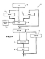
- the IBUFFER 30 is separated into five major functional sections: IBEX 64 & IBEX2 66, ROTATOR 68, SHIFTER 70, MERGE MULTIPLEXER 72, and IBUF 74.
- a pair of prefetching buffers IBEX 64 and IBEX2 66 are disposed intermediate the decoder 32 and the VIC 28.
- IBEX 64 and IBEX2 66 are quadword buffers functionally positioned between the VIC 28 and the IBUF 74 and operational to retrieve the next sequential quadword of ISTREAM while the decoder 32 is operating on the present instruction.
- This prefetching normally hides the time required for a VIC access by performing the instruction fetch during the time in which the decoder 32 is busy. Any one of the quadwords stored in the VIC 28 is controllably storable in the IBEX 64 and IBEX2 66.
- the PREFETCH PC controls operation of the VIC 28 to select and deliver a quadword of ISTREAM.
- the quadword currently selected by the PREFETCH PC is stored in the IBEX 64 while the next subsequent quadword of ISTREAM is retrieved from the VIC 28 and stored in the IBEX2 66.
- the purpose of the IBEX 64 and IBEX2 66 is to prefetch the subsequent two quadwords of ISTREAM and sequentially provide these bytes of ISTREAM to fill the IBUF 74 as each instruction is consumed by the instruction decoder 32.
- the present computer system preferably employs an instruction set which is of the variable length type. Accordingly, until the instruction decoder 32 actually decodes the opcode of the instruction, the number of bytes dedicated to the instant instruction is not "known" by the IBUFFER 30. Therefore, the IBUFFER 30 does not "know" how many bytes will be consumed by the instruction decoder 32 and will need to be refilled by the IBUFFER 30.
- the logic which controls the operation of the IBEX 64, IBEX2 66, and VIC 28 must be capable of determining the number of bytes needed to fill the decoder 32, which location or multiple locations contain the desired bytes, and whether those bytes are valid.
- the control logic for operating the IBEX 64, IBEX2 66, and VIC 28 includes a multiplexer 76 with control logic 78 operating the select inputs of the multiplexer 76.
- the IBEX 64, IBEX2 66, and VIC 28 each includes an 8-byte wide data path connected to the inputs of the multiplexer 76 such that any input may be selected by the control logic 78 and delivered over an 8-byte wide data path to the rotator 68 and to the IBEX 64.
- the IBEX2 66 is connected directly to the VIC 28 and receives the next sequential quadword of ISTREAM over the 8-byte data path therebetween. Operation of the multiplexer 76 and control logic 78 is discussed in greater detail in conjunction with the description accompanying FIGS. 9 and 10.
- the merge multiplexer 72, rotator 68 and shifter 70 interact to maintain the 9-byte instruction decoder 32 filled with the next nine sequential bytes of ISTREAM.
- the rotator 68 acts to provide the next sequential bytes of ISTREAM to replace those bytes which were discarded.
- the instruction buffer 30 attempts to provide at least the next 9-bytes of ISTREAM to the instruction decoder 32. Therefore, independent of the length of the present instruction, the decoder 32 is assured that for the majority of instructions (relatively few instructions require more than 9 bytes) the entire instruction is present and available for decoding.
- the IBUF 74 is a 9-byte register for storing the results of the merge multiplexer 72 until the decoder 32 is available to accept the ISTREAM. Further, the output of the IBUF 74 is also connected to the input of the shifter 70.
- the IBUF 74 is linked to the instruction decoder 32 by a data path 80 for conveying the values of up to nine bytes of an instruction currently being decoded. Associated with the eight bits of each byte is a parity bit for detecting any single bit errors in the byte, and also a valid data flag for indicating whether the IBUF 74 has, in fact, been filled with data from the VIC 28 as requested by the program counter 26.
- the instruction decoder 32 decodes a variable number of specifiers depending upon the particular opcode being decoded, the amount of valid data in the IBUF 74, and whether the downstream stages in the pipeline are available to accept more specifiers. Specifically, the instruction decoder 32 inspects the opcode to determine the number of subsequent bytes which are associated with that particular instruction. Then the decoder 32 checks the valid data flags to determine how many of the associated specifiers that can be decoded and then decodes these specifiers in a single cycle. The instruction decoder 32 delivers a signal indicating the number of bytes that were decoded in order to remove these bytes from the IBUF 74.
- the decoder inspects the valid bytes to ensure that these four bytes are valid and then decodes these specifiers. Thereafter, the decoder instructs the shifter 70 to remove the opcode and the consumed four bytes and move the upper four bytes into the low order four byte locations. This shifting process is effective to move the next opcode into the zero byte location of the IBUF 74.
- the IBUF 74 need not be large enough to hold an entire instruction, so long as it may hold at least three specifiers of the kind which are typically found in an instruction.
- the instruction decoder 32 is somewhat simplified if the byte 0 position of the IBUF 74 holds the opcode while the other bytes of the instruction are shifted into and out of the IBUF 74. In effect, the IBUF 74 holds the opcode in byte 0 and functions as a first-in, first-out buffer for byte positions 1 through 8.
- the instruction decoder 32 is also simplified by the operating criteria that only the specifiers for a single instruction are decoded during each cycle of the system clock.
- the instruction decoder 32 transmits a "shift opcode" signal to the shifter 70 in order to shift the opcode out of the byte 0 position of the IBUF 74 so that the next opcode may be received in the byte 0 position.
- the VIC 28 is preferably arranged to receive and transmit instruction data in blocks of multiple bytes of data.
- the block size is preferably a power of two so that the blocks have memory addresses specified by a certain number of most significant bits in the address provided by the program counter 26.
- each block consists of 32-bytes or four quadwords and is addressed by a 32-bit address.
- bits 31-5 are unique for each block.
- the address of the opcodes within the ISTREAM occur at various positions within the block.
- the rotator 68 is disposed in the data path from the VIC 28 to the IBUF 74.
- the rotator 68, as well as the shifter 70, are comprised of cross-bar switches.
- the data path from the VIC 28 includes eight parallel busses, one bus being provided for each byte of the ISTREAM.
- IBUF VALID COUNT 81 The number of valid bytes at any particular instance is kept in a register called IBUF VALID COUNT 81. The value of this register is the previous IBUF VALID COUNT minus the number of bytes shifted plus the number of new bytes merged through MERGE MUX 72. Similarly it is necessary to know how many bytes remain in IBEX 64. Any bytes that have been moved into the IBUF 74 are considered invalid. As IBUF 64 becomes full the remaining bytes from the quadword of data or a complete new quadword are stored in IBEX.
- IBEX VALID COUNT The number of valid bytes in IBEX is stored in a 'virtual' register called IBEX VALID COUNT. This is not a hardware register but the output from combinational logic that produces either, the previous IBEX VALID COUNT minus the number of bytes merged into the IBUF 74 if IBEX is being selected into MUX 76, or eight bytes minus the number of bytes merged into the IBUF 74 if IBEX 2 or VIC is selected into MUX 76.
- combinational logic 82 controlling the merge multiplexer 72 receives a IBUF VALID COUNT of zero so that all of the select lines S0-S8 are not asserted and the merge multiplexer 72 selects data from only the B0 to B8 inputs. Since none of the instructions in the IBUF 74 are valid they are discarded, and only the new instructions contained in ROTATOR 68 are presented to the IBUF 74.
- the MERGE MUX 72 is used to select the number of bytes from the ROTATOR 68 to be merged with a select number of bytes from the shifter 70. If the signal SHIFT OP is asserted the output of the SHIFTER 70 will be the IBUF 74 bytes 0 through 8 shifted down by the number to shift, otherwise if SHIFT OP is not asserted the output of the shifter will be IBUF 74 byte 0 in position A0 with IBUF 74 bytes 1 through 9 shifted down by the number of bytes to shift.
- the IBUF 74 when the IBUF 74 is initially loaded, there will be an offset between the address corresponding to the opcode in the data from VIC 28. In particular, this offset is given by the least significant bits of the program counter 26. As shown in FIG. 5 a quadword of ISTREAM (eight bytes) is delivered to the ROTATOR 68, thus using the three least significant bits from the program counter 26 as the rotate value the opcode byte is delivered to the B0 input of merge mux 72. For example, if the program branches to BOD 16 i.e., the fifth byte of the second quadword in a block. The quadword address is B08 16, the least significant three bits are 5, so when the VIC provides the quadword the ROTATOR 67 rotates by 5 bytes and delivers byte 5 to the B0 input of MERGE MUX 72.
- rotate value 8 - IBEX_VALID_COUNT- (IBUF_VALID_COUNT - NO._BYTES TO SHIFT)
- the rotate value is minus two, therefore the rotator shifts up by two (as the result was negative).
- the rotator 68 delivers byte 5 of the quadword in IBEX 64 to the B7 input on merge mux 72, and byte 6 to B8 (byte 7 is of no interest as it will not be merged, it is however, delivered to the B0 input). Positive rotate values will cause the ROTATOR 68 to shift down.
- combinational logic 90 controlling the rotator 68 calculates the relevant rotate value.
- the merge value is five so S1, S2, S3, S4 select the output from the SHIFTER 70 but S5, S6, S7, S8 select the output from the ROTATOR 68.
- the ROTATOR 68 receives eight bytes of data but transmits nine bytes to the MERGE MUX 72, the nine bytes delivered to B0 - B8 inputs are never all valid.
- the ninth byte gets the same data as the first byte but it is only valid when the rotate value is negative.
- the instruction decoder 32 examines it and the other bytes in the IBUF 74 to determine whether it is possible to simultaneously decode up to three operand specifiers.
- the instruction decoder 32 further separates the source operands from the destination operands, In particular, in a single cycle of the system clock, the instruction decoder 32 may decode up to two source operands and one destination operand. Flags indicating whether source operands or a destination operand are decoded for each cycle are transmitted from the instruction decoder 32 to the OPU 34.
- the instruction decoder 32 simultaneously decodes up to three register specifiers per cycle. When a register specifier is decoded, its register address is placed on the transfer bus TR and sent to the source list queue 38 via a transfer unit 92 in the OPU 34.
- the instruction decoder 32 may decode one short literal specifier per cycle. According to the VAX instruction architecture, the short literal specifier must be a source operand specifier. When the instruction decoder 32 decodes a short literal specifier, the short literal data is transmitted over a bus (EX) to an expansion unit 94 in the OPU 34.
- EX bus
- the instruction decoder 32 is capable of decoding one complex specifier per cycle.
- the complex specifier data is transmitted by the instruction decoder 32 over a general purpose bus (GP) to a general purpose unit 96 in the OPU 34.
- GP general purpose bus
- the instruction decoder 32 transmits the "shift op" signal to the shifter 70.
- the instruction decoder and also transmits a microprogram "fork” address to a fork queue in the queues 36, as soon as a valid opcode is received by the IBUF 74.
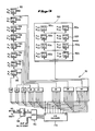
- FIG. 6 a schematic diagram of the shifter 70 is shown.
- the A0-A8 byte inputs of the merge multiplexer 72 are illustrated connected to the 8-bit outputs of a bank of multiplexers which comprise the shifter 70. It should be remembered that the purpose of the shifter 70 is to move the unused portion of the instruction stream contained in the IBUF 74 into those bytes of the IBUF 74 which were previously consumed by the instruction decoder 32.
- the instruction decoder 32 used the three lowest bytes (0, 1, 2) of the IBUF 74, then in order to properly present the next instruction to the decoder 32, it is preferable to shift the remaining valid six bytes (3-8) into the low order six bytes of the IBUF 74.
- the consumed low order bytes are no longer of any immediate use to the decoder 32 and are discarded.
- the shifter 70 need only move high order bytes into low order byte positions and does not rotate the low order bytes into the high order byte positions. This requirement simplifies the shifter configuration for the higher order bytes since each byte position only receives shifted bytes from those positions which are relatively higher. For example, byte position six only receives shifted bytes from its two higher order positions (7 and 8), while byte position one receives shifted bytes from its seven higher order positions (2-8).
- the multiplexer bank 102 receives bytes 6, 7, and 8 from the IBUF 74 and delivers an output to the A6 input of the merge multiplexer 72.
- Within the multiplexer bank 102 is a group of eight 3-input multiplexers 102a-102h.
- the multiplexer 102a receives the zero bit of each of the input bytes 6, 7, and 8 at input locations 0, 1, and 2 respectively.
- the multiplexers 102b-102h receive bits 1-7 respectively of the three input bytes.
- the select lines for each of the multiplexers 102a-102h is connected to the instruction decoder 32 and carries the 3-bit signal "number to shift".
- the "number to shift" signal is, of course, the number of bytes that were consumed by the instruction decoder 32.
- the select lines of the multiplexers 102a-102h act to deliver all eight bits of the selected byte. For example, if the decoder 32 consumes two bytes of the ISTREAM, then the contents of the IBUF 74 are shifted by two bytes, such that byte eight is moved into sixth byte location. Accordingly, the "number to shift" signal is set to the value two, thereby selecting the third input to the multiplexers 102a-102h. Thus, the byte eight position is selected and delivered to the merge multiplexer input A6.
- the internal structure of the remaining multiplexer banks 104-114 are substantially similar, varying only in the number of input bytes.
- the multiplexer bank 114 has an output connected to the A7 input of the merge multiplexer 72.
- the inputs to the multiplexer 114 include only bytes 7 and 8 of the IBUF 74.
- the multiplexer bank 112 has an output connected to the A5 input of the merge multiplexer 72.
- the inputs to the multiplexer 112 include bytes 5, 6, 7, and 8 of the IBUF 74.
- the multiplexer bank 110 has an output connected to the A4 input of the merge multiplexer 72.
- the inputs to the multiplexer 110 include bytes 4, 5, 6, 7, and 8 of the IBUF 74.
- the multiplexer bank 108 has an output connected to the A3 input of the merge multiplexer 72.
- the inputs to the multiplexer 108 include bytes 3, 4, 5, 6, 7, and 8 of the IBUF 74.
- the multiplexer bank 106 has an output connected to the A2 input of the merge multiplexer 72.
- the inputs to the multiplexer 106 include bytes 2, 3, 4, 5, 6, 7, and 8 of the IBUF 74.
- the multiplexer bank 104 differs slightly from the other multiplexer banks, in that its output is directly connected to the merge multiplexer 72 and also the zero byte position of the IBUF 74.
- the byte zero case is additionally complicated by a requirement that in addition to the shifter 70 being capable of moving any of the higher order bytes into the zero byte position, the shifter 70 must also be capable of retaining the current zero byte while the remaining bytes are shifted. This feature is desired because byte zero contains the opcode. Thus, if the specifiers extend beyond the length of the IBUF 74, then the consumed bytes must be shifted out and new specifiers rotated in, but the opcode must remain until the entire instruction is decoded.
- the inputs to the multiplexer 104 include bytes 1, 2, 3, 4, 5, 6, 7, and 8 of the IBUF 74.
- the output of the multiplexer 104 is delivered to one input of a bank of multiplexers 116.
- the second input to the multiplexer bank 116 is connected to the zero byte position of the IBUF 74.
- a single bit select line is connected to the instruction decoder 32 through an OR gate 118, so that when the instruction decoder 32 issues either a "shift opcode" or an "FD shift opcode" signal, the select line is asserted and the output of the multiplexer 104 is delivered to the A0 input of the merge multiplexer 72. Otherwise, if neither of these signals is asserted, then byte 0 is selected and delivered to the A0 input of the merge multiplexer 72.
- FIG. 7 there is shown a schematic diagram of the rotator 68.
- the B0-B8 byte inputs of the merge multiplexer 72 are illustrated as connected to the 8-bit outputs of a bank of multiplexers which comprise the rotator 68.
- the purpose of the rotator 68 is to rotate the next quadword of ISTREAM so that the merge multiplexer 72 can fill the IBUF 74 with the valid low order bytes of the shifter 70 and the rotated high order bytes of the rotator 68.
- each of the multiplexer banks in the rotator 68 is capable of delivering any of the input bytes at its output.
- the shifter 70 moves the remaining valid six bytes (3-8) into the low order six bytes (0-5) of merge multiplexer inputs A0-A5.
- the rotator 68 rotates its low order three bytes into positions 6, 7, and 8 so that the merge multiplexer 72 can combine A0-A5 and B6-B8 to fill the IBUF 74.
- the low order three bytes available from the multiplexer 76 could be the low order three bytes of IBEX2 66 or the VIC 28 or any three consecutive bytes of IBEX 64.
- the multiplexer bank 132 receives bytes 0-7 from either the VIC 28, IBEX 64, or IBEX2 66, as described in conjunction with FIGS. 4, 9, and 10.
- the output of the multiplexer bank 132 is delivered to the B4 input of the merge multiplexer 72.
- Within the multiplexer bank 132 is a group of eight 8-input multiplexers 132a-132h.
- the multiplexer 132a receives the zero bit of each of the input bytes 0-7 at multiplexer 132a input locations 4-3 respectively.
- the multiplexers 132b-132h receive bits 1-7 respectively of all of the eight input bytes.
- the select lines for each of the multiplexers 132a-132h receives the 3-bit rotate value as described in conjunction with FIG. 5.
- the signal is, of course, the number of bytes positions that the ISTREAM should be rotated to properly fill the IBUF 74.
- the multiplexers 132a-132h will each select the input located at position three. Accordingly, bits 0-7 of input byte seven are selected and delivered to the B4 input of the merge multiplexer 72. Therefore, in response to a request for a three byte rotate, the input byte seven is delivered to byte position four.
- the remaining multiplexer banks 134-148 are substantially similar to the multiplexer bank 132, differing only in the order in which the input bytes are connected to the multiplexer banks 132-148. For example, the same request for a three byte rotate causes multiplexer bank 140 to deliver the sixth input byte to byte position three (B3).
- the rotator 68 rotates its contents so that positions B0-B8 of the merge multiplexer 72 respectively receive positions 3, 4, 5, 6, 7, 8, 0, 1, 2. Therefore, the merge multiplexer successfully combines the two inputs to deliver the next nine bytes of ISTREAM to the IBUF 74 by selecting inputs A0-A5 and B6-B8.
- FIG. 8 there is shown a schematic diagram of the merge multiplexer 72 and merge multiplexer control logic 82. It should be remembered that the merge multiplexer 72 operates under control of the logic 82 to select the next nine bytes of ISTREAM from the two sets of 9 byte inputs from the rotator 68 and shifter 70. Generally, the low order bytes are selected from the shifter 70 while the rotator 68 fills the remaining high order byte positions.
- the control logic 82 receives the "number to shift" signal (m) and the IBUF VALID COUNT and uses the values of these signals to select the proper input bytes.
- the merge multiplexer 72 includes nine banks of multiplexers 150, 152, 154, 156, 158, 160, 162, 164, 166 with each bank receiving two byte position inputs, one byte each from the rotator 68 and shifter 70.
- the select line connected to each bank of multiplexers is asserted to select the rotator input and unasserted to select the shifter input.
- the multiplexer bank 150 receives bits 0-7 from the zero byte position of both the shifter 70 (A00-A07) and rotator 68 (B00-B07). The output of the multiplexer bank 150 is delivered to the zero byte position of the IBUF 74. Contained within the multiplexer bank 150 is a group of eight 2-input multiplexers 150a-150h.
- the multiplexer 150a receives the zero bit of both of the zero position input bytes such that an asserted value on the select line delivers B00 and an unasserted value delivers A00.
- the multiplexers 150b-150h receive bits 1-7 respectively of both of the input bytes.
- the select lines for each of the multiplexers 150a-150h receives a 1-bit select signal from the priority decoder 82 in order to commonly deliver all eight bits of the selected byte to the zero input position of the IBUF 74.
- the "number to shift" signal (m) is subtracted from the IBUF VALID COUNT to determine the lowest order byte position into which the rotator inputs should be delivered.
- the signal m is delivered to a 1s complement generator 168 to convert the signal m into a negative value.
- the signal -m is delivered to an adder 170 which performs the arithmetic operation and delivers the result to a 4:16 decoder 172. Accordingly, the lower order nine output bits of the decoder produce a single asserted signal at the numeric position corresponding to the lowest order byte position into which the rotator inputs should be delivered. Therefore, this asserted byte position and all higher order byte positions should be asserted to properly select rotator inputs at the corresponding multiplexers.
- the rotator inputs should be selected for byte positions 6 through 8.
- the output of the decoder 172 asserts only the line corresponding to byte position 6.
- a bank of OR gates 174 are connected to the outputs of the decoder 172 to provide asserted signals to the multiplexers corresponding to the asserted line and all higher order byte positions.
- the "number to shift" signal controls the operation of the merge multiplexer 72.
- the "number to shift” signal is zero and the IBUF VALID COUNT is zero and the entire contents of the rotator 68 are loaded into the IBUF 74. Therefore, the output of the adder 170 is zero, enabling all of the outputs of the bank of OR gates 82.
- the select lines to the multiplexers 150-166 all act to select the B inputs and pass the entire contents of the rotator to the IBUF 74.
- the control logic 78 for operating the multiplexer 76 of FIG. 4 selects either IBEX 64, IBEX2 66 or VIC 28 according to the following priority scheme.
- the control logic 78 selects IBEX 64, IBEX2 66 or VIC 28 with a simple priority algorithm. If IBEX is not empty then IBEX 64 is delivered to the ROTATOR 68 otherwise if IBEX2 is valid it is delivered to the rotation 68 and if both IBEX is empty and IBEX2 is not valid VIC data is delivered to the ROTATOR 68.
- IBEX is loaded each cycle with the data delivered by MUX 76 but it is marked empty either on a FLUSH or when all valid data on the ROTATOR 68 is consumed by the IBUF 74.
- IBEX VALID COUNT becomes non-zero when MUX 76 provides data to ROTATOR 68 that cannot find a place in IBUF 74.
- IBEX 64 and IBEX 2 are cleared (FLUSHED) and the VIC is accessed for the new ISTREAM. Assume it branches to the first byte of a block that is in the VIC 28.
- the first quadword from the VIC 28 is presented to MUX 76 this passes the data through the ROTATOR 68 and MERGE MUX to IBUF 74. IBEX is loaded with the data but is not marked valid as all eight bytes went into the IBUF 74. In the following cycle the VIC 28 presents the second quadword to MUX 76 which passes it to the ROTATOR 68.
- IBEX2 can be considered stall buffer for the VIC 28. Because of the pipelined nature of creating a new prefetch address, accessing the VIC strams then checking for a VIC HIT it is impractical to stop this process as soon as IBEX contains some valid bytes. Thus data from the VIC 28 is loaded into IBEX2 66 the cycle after IBEX 64 is loaded with some valid data and IBEX2 66 is marked valid if it is a VIC HIT. Taking the above example, where a branch to the first byte of a valid block in the VIC 28 is executed. The address of the first quadword is moved to PREFETCH PC in the first cycle.
- the first quadword is delivered to IBUF 74 and PREFETCH PC moves on to the second quadword.
- the second quadword is delivered to IBUF 74 and IBEX 64 and the PREFETCH PC moves to the third quadword.
- the fourth cycle assuming DECODER 32 consumes no more bytes, the third quadword is delivered to IBEX2 and PREFETCH PC moves to the fourth quadword and 15 we decide to stall.
- the VIC 28 delivers the fourth quadword to MUX 76 but IBEX 64 data is passed to the ROTATOR 68.
- prefetching of ISTREAM can move significantly ahead of the instruction in the IBUF.
- One benefit of the VIC 28 is that accesses to the main cache 22 are significantly reduced. However, this benefit will be severely reduced if prefetching continues too far ahead of the decoded instruction stream.
- a branch instruction occurs once in every sixteen bytes of ISTREAM so it is essential that prefetching does not access the main cache 22 unless there is a reasonable chance the data will be used.
- a request to the main cache for data is only made if there is a VIC MISS, IBEX2 is not valid and IBEX is empty. This usually means seven or eight bytes are still available to the DECODER 32 when the request for a VIC block is made.
- FIG. 9 there is shown a block diagram of the two-unit valid block store stram 58 of the virtual instruction cache 28. Since the VIC 28 is a virtual cache, it must be flushed on a context switch or REI instruction. In other words, all 256 of the 1-bit storage locations must be marked as invalid. Unfortunately, only one storage location can be marked as invalid during each clock cycle. Accordingly, it is possible that if all 256 bits are set to their valid condition, then it takes 256 clock cycles to clear the block valid stram 58.
- each stram 220, 222 is configured to perform either hit/miss determination or valid bit clearing. In fact, each context switch causes BVSA and BVSB to switch to the opposite function.
- BVSA and BVSB each receive a single 8-bit address from respective multiplexers 224, 226. Both of the multiplexers 224, 226 receive a pair of addresses from the PC 26 and a reset control 228. In order to present the PC address to one of the strams 220, 222 and the reset address to the other stram 220, 222, the select lines to the multiplexers 224, 226 are operated in a complementary fashion.
- the reset control 228 receives a CONTEXT SWITCH signal from the execution unit 20 and begins to sequentially present address 0-255 to the multiplexers 224, 226.
- One of the multiplexers 224, 226 passes these sequential addresses to the selected strams 220, 222, such that the 256 valid bits contained therein are reset over a period of 256 clock cycles.
- the reset control delivers a handshaking signal to indicate that the reset process is complete.
- An S-R flip flop 230 receives the handshaking signal at its set input, causing the flip flop 230 to latch a PROCEED WITH CONTEXT SWITCH SIGNAL to the execution unit 20.
- the SWITCH CONTEXT signal from the execution unit 20 is also connected to the reset input of the flip flop 230 so that the PROCEED WITH CONTEXT SWITCH signal is reset at the beginning of each context switch.
- Control of the select lines to the multiplexers 224, 226 is provided by a J-K flip flop 232 which toggles between asserted and unasserted in response to each CONTEXT SWITCH signal. Both inputs of the flip flop 232 are connected to a logical "1" and the clock input is connected to the CONTEXT SWITCH signal. Thus, the Q output (USE BLOCK B) of the flip-flop 232 switches between "0" and "1" in response to a transition in the SWITCH CONTEXT signal.
- the select input of the multiplexer 224 is connected directly to the Q output of the flip-flop 232, while the select input of the multiplexer 226 is connected to the Q output of the flip-flop 232 through an inverter 234.
- the block valid data (MARKER BLOCK VALID) from the PC unit (26 in FIG. 1) is multiplexed between the data inputs of the strams 220, 222 in response to the USE BLOCK B SIGNAL.
- the data input of the "B" stram 222 is connected to the MARKER BLOCK VALID line through an AND gate 237 which is enabled by the USE BLOCK B signal
- the data input of the "A" stram 220 is connected to the MARKER BLOCK VALID line through an AND gate enabled by the complement of the USE BLOCK B signal as provided by an inverter 239.
- the MARKER BLOCK VALID data is fed into the "B" stram 222 while the "A" stram receives zero data and is therefore cleared. Conversely, when the USE BLOCK B signal is not asserted, the MARKER BLOCK VALID data is fed into the "A" stram 222 while the "B” stram receives zero data and is therefore cleared.
- the valid bit outputs of the strams 220, 222 are connected to a pair of inputs to a multiplexer 236.
- the select line of the multiplexer 236 is also connected to the Q output of the flip flop 232 to operate in conjunction with the multiplexers 224, 226. Accordingly, the stram 220, 222 which is selected to receive the PC address is also selected to deliver its output as the BLOCK VALID BIT.
Abstract
Description
- This invention relates generally to an instruction buffer system and to a virtual instruction cache (VIC) of a high-speed digital computer.
- In the field of high speed computers, most advanced computers pipeline the entire sequence of instruction activities. A prime example is the VAX 8600 computer manufactured and sold by Digital Equipment Corporation, 111 Powdermill Road, Maynard MA 97154-1418. The instruction pipeline for the VAX 8600 is described in T. Fossum et al. "An overview of the VAX 8600 System", Digital Technical Journal, No. 1, August 1985, pp. 8-23. Separate pipeline stages are provided for instruction fetch, instruction decode, operand address generation, operand fetch, instruction execute, and result store.
- To make effective use of this pipelining capability, it is desirable to keep each stage of the pipeline occupied, performing its intended function on the next instruction to be executed. In order to do this, the instruction fetch stage must retrieve an instruction and pass it to the next stage between each transition of the system clock. Otherwise, such a disruption in the instruction stream causes the pipeline to drain, necessitating a time-consuming restart of the entire pipeline. Of course, the purpose of the pipeline is to increase the overall speed of the computer. Thus, it is highly advantageous to avoid these situations where the pipeline is interrupted.
- However, the instruction set employed in some computers is of the variable length type, thereby forcing the instruction buffer to have added complexity. In other words, until the instruction (opcode) is decoded, the instruction buffer does not "know" how many of the subsequent bytes of the instruction stream belong with the current instruction. Therefore, the instruction buffer can only respond by loading a preselected number of bytes of the instruction stream, which may or may not include an entire instruction. The instruction decoder will only consume those bytes associated with the immediate instruction. Thereafter, the instruction buffer must determine how many of the present bytes were used by the decoder, shift the unused bytes into the lowest order locations, and then fill the empty buffer locations with subsequent bytes of the instruction stream.
- Reference to the main memory to retrieve these subsequent bytes of instruction stream necessarily involves multiple clock cycles. To avoid accessing main memory, many digital computers include a high speed cache between the processing unit and the main memory. Access to this cache takes only a small number of cycles of the processor's clock but often involves translating virtual addresses to physical addresses. To further accelerate the access to the instruction stream, some systems dedicate a cache solely to store the instructions. The access to this "instruction cache" often does not entail translating from virtual to physical addresses as the instructions are stored under their virtual addresses. This access to the instruction stream in a high speed virtual instruction cache may only involve one cycle of the processor's clock. The virtual instruction cache, however, contains only a portion of the main memory, each reference to the virtual instruction cache involves comparing the requested address with the desired address to first determine if the desired instruction stream is present and then retrieving the requested instruction stream. Therefore, owing to the variable length nature of the instruction set, the instruction buffer cannot predict whether a reference to the VIC will be required by the instruction currently being decoded.
- To prevent numerous references to the virtual instruction cache, a prefetch buffer is provided to maintain a preselected number of the subsequent bytes of instruction stream which are expected to be used by the instruction decoder. This process forestalls the inevitable reference to the virtual instruction cache.
- Since the virtual instruction cache contains only a portion of the instruction stream, refills to the instruction buffer can result in "misses" in the virtual instruction cache, which require fetches from the main memory. These main memory fetches generally require many clock cycles, thereby interrupting the pipeline.
- To ensure that the instruction pipeline of a digital computer remains full to provide for fast and efficient execution of the instructions, an instruction buffer includes first and second prefetch buffers for storing a preselected number of subsequent bytes of instruction stream. The first prefetch buffer is independently addressable to retrieve a selected number of sequential bytes contained therein. Means are provided for refilling the decoder with the number of sequential bytes of instruction stream corresponding to the number of bytes currently being decoded. The refill means retrieves the instruction stream bytes from the first prefetch buffer sequentially and sets a "valid bit" corresponding to each byte of instruction stream retrieved. The second instruction buffer need only contain all valid or all invalid bytes, and therefore only one valid bit need be held for the second instruction buffer. The first prefetch buffer is refilled with the preselected number of subsequent instruction stream bytes in response to all of the valid bits corresponding to each byte of the instruction stream contained therein being clear. Similarly, the second prefetch buffer is refilled with the preselected number of subsequent instruction stream bytes when it becomes empty.
- Other objects and advantages of the invention will become apparent upon reading the following detailed description and upon reference to the drawings in which:
- FIG. 1 is a top level block diagram of a portion of a central processing unit and associated memory;
- Fig. 2 is a functional diagram of the pipeline processing of a longword ADD operand;
- FIG. 3 is a block diagram of the virtual instruction cache;
- FIG. 4 is a general block diagram of the instruction buffer interfaced with the virtual instruction cache;
- FIG. 5 is a detailed block diagram of the instruction buffer and the interface to the instruction decoder;
- FIG. 6 is a schematic diagram of the shifter of the instruction buffer;
- FIG. 7 is a schematic diagram of the rotator of the instruction buffer;
- FIG. 8 is a schematic diagram of the merge multiplexer of the instruction buffer; and
- FIG. 9 is a block diagram of the two-unit valid block store strams of the virtual instruction cache.
- While the invention is susceptible to various modifications and alternative forms, specific embodiments thereof have been shown by way of example in the drawings and will herein be described in detail. It should be understood, however, that it is not intended to limit the invention to the particular forms disclosed, but on the contrary, the intention is to cover all modifications, equivalents, and alternatives falling within the spirit and scope of the invention as defined by the appended claims.
- Turning now to the drawings, FIGURE 1 is a top level block diagram of a portion of a pipelined
computer system 10. Thesystem 10 includes at least one central processing unit (CPU) 12 having access tomain memory 14. It should be understood that additional CPUs could be used in such a system by sharing themain memory 14. - Inside the
CPU 12, the execution of an individual instruction is broken down into multiple smaller tasks. These tasks are performed by dedicated, separate, independent functional units that are optimized for that purpose. - Although each instruction ultimately performs a different operation, many of the smaller tasks into which each instruction is broken are common to all instructions. Generally, the following steps are performed during the execution of an instruction: instruction fetch, instruction decode, operand fetch, execution, and result store. Thus, by the use of dedicated hardware stages, the steps can be overlapped, thereby increasing the total instruction throughput.
- The data path through the pipeline includes a respective set of registers for transferring the results of each pipeline stage to the next pipeline stage. These transfer registers are clocked in response to a common system clock. For example, during a first clock cycle, the first instruction is fetched by hardware dedicated to instruction fetch. During the second clock cycle, the fetched instruction is transferred and decoded by instruction decode hardware, but, at the same time, the next instruction is fetched by the instruction fetch hardware. During the third clock cycle, each instruction is shifted to the next stage of the pipeline and a new instruction is fetched. Thus, after the pipeline is filled, an instruction will be completely executed at the end of each clock cycle.
- This process is analogous to an assembly line in a manufacturing environment. Each worker is dedicated to performing a single task on every product that passes through his or her work stage. As each task is performed the product comes closer to completion. At the final stage, each time the worker performs his or her assigned task a completed product rolls off the assembly line.
- As shown in FIG. 1, each
CPU 12 is partitioned into at least three functional units: thememory access unit 16, theinstruction unit 18, and theexecution unit 20. - The
memory access unit 16 includes amain cache 22 which, on an average basis, enables the instruction andexecution units main memory 14. Thiscache 22 includes means for storing selected predefined blocks of data elements, means for receiving requests from theinstruction unit 18 via atranslation buffer 24 to access a specified data element, means for checking whether the data element is in a block stored in thecache 22, and means operative when data for the block including the specified data element is not so stored for reading the specified block of data in thecache 22. In other words, the cache provides a "window" into the main memory, and contains data likely to be needed by the instruction andexecution units - If a data element needed by the instruction and
execution units cache 22, then the data element is obtained from themain memory 14, but in the process, an entire block, including additional data, is obtained from themain memory 14 and written into thecache 22. Due to the principle of locality in time and memory space, the next time the instruction and execution units desire a data element, there is a high degree of likelihood that this data element will be found in the block which includes the previously addressed data element. Consequently, it is probable that thecache 22 will already include the data element required by the instruction andexecution units cache 22 is accessed at a much higher rate than themain memory 14, themain memory 14 can have a proportionally slower access time than thecache 22 without substantially degrading the average performance of thecomputer system 10. Therefore, themain memory 14 is constructed of slower and less expensive memory elements. - The
translation buffer 24 is a high speed associative memory which stores the most recently used virtual-to-physical address translations. In a virtual memory system, a reference to a single virtual address can cause several memory references before the desired information is made available. However, where thetranslation buffer 24 is used, translation is reduced to simply finding a "hit" in thetranslation buffer 24. - The
instruction unit 18 includes aprogram counter 26 and a virtual instruction cache (VIC) 28 for fetching instructions from themain cache 22. Theprogram counter 26 preferably addresses virtual memory locations rather than the physical memory locations of themain memory 14 and thecache 22. Thus, the virtual address of theprogram counter 26 must be translated into the physical address of themain memory 14 before instructions can be retrieved. Accordingly, the contents of theprogram counter 26 are transferred to thememory access unit 16 where thetranslation buffer 24 performs the address conversion. The instruction is retrieved from its physical memory location in thecache 22 using the converted address. Thecache 22 delivers the instruction over data return lines to theVIC 28. - Generally, the
VIC 28 contains prestored instructions at the addresses specified by theprogram counter 26, and the addressed instructions are available immediately for the transfer into an instruction buffer (IBUFFER) 30. From thebuffer 30, the addressed instructions are fed to aninstruction decoder 32 which decodes both the opcodes and the specifiers. An operand processing unit (OPU) 34 fetches the specified operands and supplies them to theexecution unit 20. - The
OPU 34 also produces virtual addresses. In particular, theOPU 34 produces virtual addresses for memory source (read and destination (write) operands. For the memory read operands, theOPU 34 delivers these virtual addresses to thememory access unit 16 where they are translated to physical addresses. The physical memory locations of thecache 22 are then accessed to fetch the operands for the memory source operands. - In each instruction, the first byte contains the opcode, and the following bytes are the operand specifiers to be decoded. The first byte of each specifier indicates the addressing mode for that specifier. This byte is usually broken in halves, with one-half specifying the addressing mode and the other half specifying a register to be used for addressing. The instructions preferably have a variable length, and various types of specifiers can be used with the same opcode, as disclosed in Strecker et al., U.S. Patent 4,241,397 issued December 23, 1980.
- The first step in processing the instructions is to decode the opcode portion of the instruction. The first portion of each instruction consists of its opcode which specifies the operation to be performed in the instruction, and the number and type of specifiers to be used. Decoding is accomplished using a table-look-up technique in the
instruction decoder 32. Later, theexecution unit 20 performs the specified operation by executing prestored microcode, beginning at a predetermined starting address for the specified operation. Also, thedecoder 32 determines where source-operand and destination-operand specifiers occur in the instruction and passes these specifiers to theOPU 34 for preprocessing prior to execution of the instruction. A preferred instruction decoder for use with the refill method and apparatus of the present invention is described in the above referenced D. Fite et al. U.S. patent application Serial No. , filed , and entitled "Decoding Multiple Specifiers in a Variable Length Instruction Architecture," incorporated herein by reference. - After an instruction has been decoded, the
OPU 34 parses the operand specifiers and computes their effective addresses; this process involves reading GPRS and possibly modifying the GPR contents by autoincrementing or autodecrementing. The operands are then fetched from those effective addresses and passed on to theexecution unit 20, which executes the instruction and writes the result into the destination identified by the destination pointer for that instruction. - Each time an instruction is passed to the
execution unit 20, theinstruction unit 18 sends a microcode dispatch address and a set of pointers for (1) the location in the execution unit register file where the source operands can be found, and (2) the location where the results are to be stored. Within theexecution unit 20, a set ofqueues 36 includes a fork queue for storing the microcode dispatch address, a source pointer queue for storing the source-operand locations, and a destination pointer queue for storing the destination location. Each of these queues is a FIFO buffer capable of holding the data for multiple instructions. - The
execution unit 20 also includes asource list 38, which is a multi-ported register file containing a copy of the GPRS and a list of source operands. Thus, entries in the source pointer queue will either point to GPR locations for register operands, or point to the source list for memory and literal operands. Both thememory access unit 16 and theinstruction unit 18 write entries in thesource list 38, and theexecution unit 20 reads operands out of thesource list 38 as needed to execute the instructions. For executing instructions, theexecution unit 20 includes aninstruction issue unit 40, amicrocode execution unit 42, an arithmetic and logic unit (ALU) 44, and a retireunit 46. - The present invention is particularly useful with pipelined processors. As discussed above, in a pipelined processor, the processor's instruction fetch hardware may be fetching one instruction while other hardware is decoding the operation code of a second instruction, fetching the operands of a third instruction, executing a fourth instruction, and storing the processed data of a fifth instruction. FIG. 2 illustrates a pipeline for a typical instruction such as:
ADDL3 R0,B⌃12(R1),R2
This is a long-word addition using the displacement mode of addressing. - In the first stage of the pipelined execution of this instruction, the program count (PC) of the instruction is created; this is usually accomplished either by incrementing the
program counter 26 from the previous instruction, or by using the target address of a branch instruction. The PC is then used to accessVIC 28 in the second stage of the pipeline. - In the third stage of the pipeline, the instruction data is available from the
cache 22 for use by theinstruction decoder 32, or to be loaded into theIBUFFER 30. Theinstruction decoder 32 decodes the opcode and the three specifiers in a single cycle, as will be described in more detail below. The R0 and R2 numbers are passed to theALU 44, and the R1 number along with the byte displacement is sent to theOPU 34 at the end of the decode cycle. - In stage four, the
OPU 34 reads the contents of its GPR register file at location R1, adds that value to the specified displacement (12), and sends the resulting address to thetranslation buffer 24 in thememory access unit 16, along with an OP READ request, at the end of the address generation stage. - In stage five, the
memory access unit 16 selects the address generated in stage four for execution. Using thetranslation buffer 24, thememory access unit 16 translates the virtual address to a physical address during the address translation stage. The physical address is then used to address thecache 22, which is read in stage six of the pipeline. - In stage seven of the pipeline, the instruction is issued to the
ALU 44 which adds the two operands and sends the result to the retireunit 46. Duringstage 4, the register numbers for R1 and R2, and a pointer to the source list location for the memory data, are sent to the execution unit and stored in the pointer queues. Then during the cache read stage, the execution unit looks for the two source operands in the source list. In this particular example, it finds only the register data R0, but at the end of this stage the memory data arrives and is substituted for the invalidated read-out of the register file. Thus, both operands are available in the instruction execution stage. - In the retire stage eight of the pipeline, the result data is paired with the next entry in the retire queue. Although several functional execution units can be busy at the same time, only one instruction is retired in a single cycle.
- In the last stage nine of the illustrative pipeline, the data is written into the GPR portion of the register files in both the
execution unit 20 and theinstruction unit 18. - Referring now to FIG. 3, a block diagram of the virtual instruction cache (VIC) 28 is illustrated. The
VIC 28 is constructed of four groups of self-timed rams (STRAMS), and acts as a window into themain memory 14. In this regard theVIC 28 functions in a similar fashion as themain cache 22. The first group of VIC STRAMS is the data stram 50 which provides storage space for the actual instruction stream (ISTREAM) retrieved from themain cache 22. Specifically, the data stram 50 contains 1024 storage locations, with each storage location being 64-bits in width. From the size of the data stram 50, it should be apparent that the ISTREAM is retrieved in quadword (8-byte) packets. Accordingly, the data path between themain cache 22 and theVIC 28 is also 64-bits in width and a quadword of ISTREAM can be transferred during each system clock cycle. - The
PC 26 delivers bits 12:3 of the 32-bit virtual address to the data stram 50 in order to address each quadword of ISTREAM. Bits 2:0 are unnecessary, as they are only needed to address individual bytes within each quadword. Individual byte addressiblity is not necessary for the proper operation of theVIC 28. Rather, the smallest increment of ISTREAM which can be addressed in theVIC 2 8 is a quadword. Further, the upper bits 31:13 are not used to address the data stram 50 because only 1024 quadword locations are available for storing the ISTREAM. Accordingly, the 10-bits 12:3 are sufficient to provide a unique address for each of the 1024 data storage locations (i.e. 2¹⁰=1024). - However, it should be clear that since the upper bits 31:13 are not used to address the data stram 50, there are multiple quadwords which must be stored at identical data stram locations. For example, the quadword located at address 11111111111111111110000000000 will be stored at the same data stram location as the quadword located at address 01111111111111111110000000000. Both addresses share the same lower 10-bits and must, therefore, share the same data stram storage location. In fact, each data stram location can host any one of 1,048,576 (21¹⁹=1,048,576) quadwords.
- Accordingly, in order to determine which of theses quadwords is stored in each of the data stram locations, a set of
tag strams 52 is provided. The tag strams 52 store the upper nineteen bits 31:13 of the quadword address. However, ISTREAM is retrieved from themain cache 22 in four quadword blocks. In other words, a request to themain cache 22 for the first quadword in a block causes themain cache 22 to also return the three following quadwords. Retrieving ISTREAM in blocks satisfies the principle of locality in time and memory space and aids the overall performance of theVIC 28. Accordingly, the 1024 data stram locations are identified by only 256 tag stram locations (1 for each four quadword block). Thus, thetag stram 52 contains 256 19-bit storage locations and 8-bits (12:5) of the virtual address are sufficient to identify each of the 256 storage locations (2⁸=256). - Operation of the
VIC 28 is enhanced by the method used for retrieving ISTREAM from themain cache 22. The request for ISTREAM is always quadword aligned and can be for any quadword within a block. However, themain cache 22 only responds with the requested quadword and all subsequent quadwords to fill the block. Quadwords prior to the request in the block are not returned from themain cache 22. For example, if theVIC 28 requests the third quadword in a block, only the third and fourth quadwords are returned from themain cache 22 and are written into the data stram 50. This method of retrieving ISTREAM is employed for two reasons. First, by returning the requested quadword first, rather than the first quadword in that block, the requested ISTREAM address is available immediately and the critical response time is enhanced. Second, performance models indicate that the remainder of the block is hardly used. - Since it is possible for only a portion of a block to be present in the data stram 50, it is necessary to keep track of which quadwords are valid. Therefore, a quadword
valid stram 54 is provided. A valid bit is maintained for each quadword in thedata stram 50. The quadwordvalid stram 54 is organized similar to thetag stram 52, in that it contains 256 4-bit storage locations. Each storage location corresponds to a four quadword block of data stored in the data stram 50, with each of the four valid bits corresponding to a quadword within the block. Thus, like thetag stram 52, the quadword valid stram is addressed by the eight bits 12:5 of the virtual address. - Further, however, the individual quadword valid bits must also be independently addressable in order to determine if a particular ISTREAM quadword requested by the
IBUFFER 30 is valid. Amultiplexer 56 is connected to the 4-bit output of the quadwordvalid stram 54. The select input of themultiplexer 56 is connected to quadword identifying bits 4:3 of the virtual address. For example, a request from the IBUFFER 30 for the quadword stored at location 00000000000000000001111111101000 results in the four quadword valid bits stored at location 11111111 of the quadword valid stram being delivered to themultiplexer 56. Bits 4:3 of the virtual address indicate that the first quadword (location 01) is the desired quadword. Thus, the select lines of themultiplexer 56 cause the quadword valid bit corresponding to the selected quadword to be delivered at the multiplexer output. - Finally, the fourth group of VIC strams 58 contains valid bits for each block stored in the
data stram 50. Thus, the blockvalid stram 58 contains 256 1-bit storage locations and is addressed by bits 12:5 of the virtual address. Not only is it necessary for theVIC 28 to "know" which quadwords within a block are valid, but also, theVIC 28 needs to verify that the block itself is valid. At this time it is sufficient to understand that the block valid bit must be set before theVIC 28 will allow the selected quadword to be transferred to theIBUFFER 30. However, it should be noted that the block valid stram actually consists of two sets of strams to speed operation of theVIC 28 during a flush. At any given time, a selected one of the two sets of strams stores the block valid bits which reflect the current status of the data in theVIC 28. The addressed block valid bit, representing the validity of the addressed block of data in theVIC 28, is selected by amultiplexer 236 as either the "BLOCK_A_VALID" bit from the first set of strams (set A), or the "BLOCK_B_VALID" bit from the second set of strams (set B). This aspect of theVIC 28 is discussed in greater detail in conjunction with the description of the operation of the circuit shown in FIG. 9. - During an IBUFFER request for a selected quadword of ISTREAM, the virtual address contained in the
PC 26 is delivered to theVIC 28. TheVIC 28 responds to the request by determining if the requested quadword is present in the data stram 50 and, if so, whether it is valid. Bits 31:13 of the PC virtual address are delivered to one input of a 19-bit comparator 60. The second input to thecomparator 60 is connected to the output of thetag stram 52. Previously, bits 31:13 of the address of the quadword stored in the data stram 50 were stored in thetag stram 52. Therefore, those previously stored bits 31:13 are presented as the second input to thecomparator 60. If the two addresses match, the asserted output of thecomparator 60 is delivered as one input to the 3-input ANDgate 62. At the same time, the block and quadword valid bits are also delivered as inputs to the ANDgate 62. Accordingly, if any of the three signals is not asserted, the ANDgate 62 produces a MISS signal. Conversely, if all three signals are asserted, the ANDgate 62 produces a HIT signal. A MISS signal initiates a request to themain cache 22, while a HIT signal causes thedata STRAM 50 to deliver the selected quadword of data. - The
PC 26 is actually constructed of several separate program counters. During each system clock cycle, one of two PCs (PREFETCH PC or MTAG) is selected and its virtual address is delivered to theVIC 28. Generally, the virtual address contained in the PREFETCH PC is selected and delivered to theVIC 28. The PREFETCH PC always points to the next quadword that the IBUFFER is likely to accept. In sequential code the PREFETCH PC is incremented by one quadword each time the IBUFFER accepts ISTREAM from theVIC 28. When the ISTREAM branches, the PREFETCH PC is loaded with the correct destination address. - However, when ISTREAM is requested from and delivered by the
main cache 22, the virtual address contained in the MTAG is selected and delivered to theVIC 28. When theVIC 28 receives multiple quadwords of ISTREAM from themain cache 22, the address of theVIC 28 must be incremented by a quadword in each cycle of the main cache response. The PREFETCH PC would serve this purpose if theinstruction decoder 32 could always consume all of the ISTREAM as it arrives from themain cache 22. In practice this is not always possible. Therefore, a second PC, independent from the PREFETCH PC, is used to store the ISTREAM in theVIC 28. Once the response from themain cache 22 is complete, the PREFETCH PC is again used to address theVIC 28. The MTAG is loaded with the previous value of the VIC address when there is no request to themain cache 22. - Referring now to FIG. 4, the
IBUFFER 30 is illustrated. TheIBUFFER 30 aligns the data for decoding and performs the function of increasing the processing speed of theinstruction unit 18 by prefetching subsequent sequential instructions. TheIBUFFER 30 retrieves a selected quadword of the ISTREAM and positions that quadword, such that theinstruction decoder 32 receives the instruction with the opcode positioned in the zero byte location. In order to accomplish this complex task of repositioning the ISTREAM, theIBUFFER 30 is separated into five major functional sections:IBEX 64 &IBEX2 66,ROTATOR 68,SHIFTER 70,MERGE MULTIPLEXER 72, andIBUF 74. - Rather than simply increase the size of the
instruction decoder 32 to contain more bytes of the ISTREAM, a pair ofprefetching buffers IBEX 64 andIBEX2 66 are disposed intermediate thedecoder 32 and theVIC 28.IBEX 64 andIBEX2 66 are quadword buffers functionally positioned between theVIC 28 and the IBUF 74 and operational to retrieve the next sequential quadword of ISTREAM while thedecoder 32 is operating on the present instruction. This prefetching normally hides the time required for a VIC access by performing the instruction fetch during the time in which thedecoder 32 is busy. Any one of the quadwords stored in theVIC 28 is controllably storable in theIBEX 64 andIBEX2 66. As discussed previously, the PREFETCH PC controls operation of theVIC 28 to select and deliver a quadword of ISTREAM. The quadword currently selected by the PREFETCH PC is stored in theIBEX 64 while the next subsequent quadword of ISTREAM is retrieved from theVIC 28 and stored in theIBEX2 66. - The purpose of the
IBEX 64 andIBEX2 66 is to prefetch the subsequent two quadwords of ISTREAM and sequentially provide these bytes of ISTREAM to fill the IBUF 74 as each instruction is consumed by theinstruction decoder 32. It should be noted that the present computer system preferably employs an instruction set which is of the variable length type. Accordingly, until theinstruction decoder 32 actually decodes the opcode of the instruction, the number of bytes dedicated to the instant instruction is not "known" by theIBUFFER 30. Therefore, theIBUFFER 30 does not "know" how many bytes will be consumed by theinstruction decoder 32 and will need to be refilled by theIBUFFER 30. Thus, the logic which controls the operation of theIBEX 64,IBEX2 66, andVIC 28 must be capable of determining the number of bytes needed to fill thedecoder 32, which location or multiple locations contain the desired bytes, and whether those bytes are valid. - The control logic for operating the
IBEX 64,IBEX2 66, andVIC 28 includes amultiplexer 76 withcontrol logic 78 operating the select inputs of themultiplexer 76. TheIBEX 64,IBEX2 66, andVIC 28 each includes an 8-byte wide data path connected to the inputs of themultiplexer 76 such that any input may be selected by thecontrol logic 78 and delivered over an 8-byte wide data path to therotator 68 and to theIBEX 64. TheIBEX2 66 is connected directly to theVIC 28 and receives the next sequential quadword of ISTREAM over the 8-byte data path therebetween. Operation of themultiplexer 76 andcontrol logic 78 is discussed in greater detail in conjunction with the description accompanying FIGS. 9 and 10. - The
merge multiplexer 72,rotator 68 andshifter 70 interact to maintain the 9-byte instruction decoder 32 filled with the next nine sequential bytes of ISTREAM. As thedecoder 32 completes the decoding stage of each instruction, those consumed bytes are shifted out and discarded by theshifter 70. Therotator 68 acts to provide the next sequential bytes of ISTREAM to replace those bytes which were discarded. In this manner, theinstruction buffer 30 attempts to provide at least the next 9-bytes of ISTREAM to theinstruction decoder 32. Therefore, independent of the length of the present instruction, thedecoder 32 is assured that for the majority of instructions (relatively few instructions require more than 9 bytes) the entire instruction is present and available for decoding. - The
IBUF 74 is a 9-byte register for storing the results of themerge multiplexer 72 until thedecoder 32 is available to accept the ISTREAM. Further, the output of theIBUF 74 is also connected to the input of theshifter 70. - Turning now to FIG. 5, the data paths to and from the
instruction decoder 32 are shown in greater detail. In order to simultaneously decode a number of operand specifiers, theIBUF 74 is linked to theinstruction decoder 32 by adata path 80 for conveying the values of up to nine bytes of an instruction currently being decoded. Associated with the eight bits of each byte is a parity bit for detecting any single bit errors in the byte, and also a valid data flag for indicating whether theIBUF 74 has, in fact, been filled with data from theVIC 28 as requested by theprogram counter 26. - The
instruction decoder 32 decodes a variable number of specifiers depending upon the particular opcode being decoded, the amount of valid data in theIBUF 74, and whether the downstream stages in the pipeline are available to accept more specifiers. Specifically, theinstruction decoder 32 inspects the opcode to determine the number of subsequent bytes which are associated with that particular instruction. Then thedecoder 32 checks the valid data flags to determine how many of the associated specifiers that can be decoded and then decodes these specifiers in a single cycle. Theinstruction decoder 32 delivers a signal indicating the number of bytes that were decoded in order to remove these bytes from theIBUF 74. For example, if the opcode includes four bytes of associated specifiers, the decoder inspects the valid bytes to ensure that these four bytes are valid and then decodes these specifiers. Thereafter, the decoder instructs theshifter 70 to remove the opcode and the consumed four bytes and move the upper four bytes into the low order four byte locations. This shifting process is effective to move the next opcode into the zero byte location of theIBUF 74. - The
IBUF 74 need not be large enough to hold an entire instruction, so long as it may hold at least three specifiers of the kind which are typically found in an instruction. Theinstruction decoder 32 is somewhat simplified if thebyte 0 position of theIBUF 74 holds the opcode while the other bytes of the instruction are shifted into and out of theIBUF 74. In effect, theIBUF 74 holds the opcode inbyte 0 and functions as a first-in, first-out buffer forbyte positions 1 through 8. Theinstruction decoder 32 is also simplified by the operating criteria that only the specifiers for a single instruction are decoded during each cycle of the system clock. Therefore, at the end of a cycle in which all of the specifiers for an instruction will have been decoded, theinstruction decoder 32 transmits a "shift opcode" signal to theshifter 70 in order to shift the opcode out of thebyte 0 position of theIBUF 74 so that the next opcode may be received in thebyte 0 position. - The
VIC 28 is preferably arranged to receive and transmit instruction data in blocks of multiple bytes of data. The block size is preferably a power of two so that the blocks have memory addresses specified by a certain number of most significant bits in the address provided by theprogram counter 26. For example, in the preferred embodiment, each block consists of 32-bytes or four quadwords and is addressed by a 32-bit address. Thus, bits 31-5 are unique for each block. Further, owing to the instructions being of variable length, the address of the opcodes within the ISTREAM occur at various positions within the block. To loadbyte 0 of theIBUF 74 with the next opcode to be executed, which may occur at any byte position within a block of instruction data from the cache, therotator 68 is disposed in the data path from theVIC 28 to theIBUF 74. Therotator 68, as well as theshifter 70, are comprised of cross-bar switches. The data path from theVIC 28 includes eight parallel busses, one bus being provided for each byte of the ISTREAM. - In the general case, it is necessary to keep track of the number of valid bytes in the
IBUF 74. The number of valid bytes at any particular instance is kept in a register calledIBUF VALID COUNT 81. The value of this register is the previous IBUF VALID COUNT minus the number of bytes shifted plus the number of new bytes merged throughMERGE MUX 72. Similarly it is necessary to know how many bytes remain inIBEX 64. Any bytes that have been moved into theIBUF 74 are considered invalid. AsIBUF 64 becomes full the remaining bytes from the quadword of data or a complete new quadword are stored in IBEX. The number of valid bytes in IBEX is stored in a 'virtual' register called IBEX VALID COUNT. This is not a hardware register but the output from combinational logic that produces either, the previous IBEX VALID COUNT minus the number of bytes merged into theIBUF 74 if IBEX is being selected intoMUX 76, or eight bytes minus the number of bytes merged into theIBUF 74 ifIBEX 2 or VIC is selected intoMUX 76. - At the beginning of a program or after a branch or jump instruction is executed, it is desirable to load the
IBUF 74 with entirely new data from theVIC 28. For this purpose,combinational logic 82 controlling themerge multiplexer 72 receives a IBUF VALID COUNT of zero so that all of the select lines S0-S8 are not asserted and themerge multiplexer 72 selects data from only the B0 to B8 inputs. Since none of the instructions in theIBUF 74 are valid they are discarded, and only the new instructions contained inROTATOR 68 are presented to theIBUF 74. - In order to load new ISTREAM into the
IBUF 74 from theVIC 28, theMERGE MUX 72 is used to select the number of bytes from theROTATOR 68 to be merged with a select number of bytes from theshifter 70. If the signal SHIFT OP is asserted the output of theSHIFTER 70 will be theIBUF 74bytes 0 through 8 shifted down by the number to shift, otherwise if SHIFT OP is not asserted the output of the shifter will be IBUF 74byte 0 in position A0 withIBUF 74bytes 1 through 9 shifted down by the number of bytes to shift. - Also when the
IBUF 74 is initially loaded, there will be an offset between the address corresponding to the opcode in the data fromVIC 28. In particular, this offset is given by the least significant bits of theprogram counter 26. As shown in FIG. 5 a quadword of ISTREAM (eight bytes) is delivered to theROTATOR 68, thus using the three least significant bits from theprogram counter 26 as the rotate value the opcode byte is delivered to the B0 input ofmerge mux 72. For example, if the program branches toBOD 16 i.e., the fifth byte of the second quadword in a block. The quadword address isB08 16, the least significant three bits are 5, so when the VIC provides the quadword theROTATOR 67 rotates by 5 bytes and deliversbyte 5 to the B0 input ofMERGE MUX 72. - In the general case, though, the rotate value is calculated using the formula:
rotate value = 8 - IBEX_VALID_COUNT-
(IBUF_VALID_COUNT
- NO._BYTES TO SHIFT) - For example, if there are nine valid bytes in the
IBUF 74 and three in IBEX (bytes rotator 68 deliversbyte 5 of the quadword inIBEX 64 to the B7 input onmerge mux 72, andbyte 6 to B8 (byte 7 is of no interest as it will not be merged, it is however, delivered to the B0 input). Positive rotate values will cause theROTATOR 68 to shift down. Thus,combinational logic 90 controlling therotator 68 calculates the relevant rotate value. - The control for the MERGE MUX in
combinational logic 82 produces individual select lines S0 - S8 for themerge mux 72 such that the relevant bytes from the SHIFTER and ROTATOR are delivered to theIBUF 74. If SHIFT OP is not asserted then S0 always selects the A0 input such that the opcode byte remains inbyte 0 of theIBUF 74. The remaining selects are calculated as follows:
MERGE_VALUE = IBUF_VALID_COUNT - NO._BYTES_TO_SHIFT; any select (S1-S8) less than MERGE_VALUE selects theSHIFTER 70, and the rest select theROTATOR 68. - For example, if there are eight valid bytes in the
IBUF 74 and the number to shift is three, the merge value is five so S1, S2, S3, S4 select the output from theSHIFTER 70 but S5, S6, S7, S8 select the output from theROTATOR 68. - Since the
ROTATOR 68 receives eight bytes of data but transmits nine bytes to theMERGE MUX 72, the nine bytes delivered to B0 - B8 inputs are never all valid. The ninth byte gets the same data as the first byte but it is only valid when the rotate value is negative. - Once an opcode has been loaded into the
byte 0 position of theIBUF 74, theinstruction decoder 32 examines it and the other bytes in theIBUF 74 to determine whether it is possible to simultaneously decode up to three operand specifiers. Theinstruction decoder 32 further separates the source operands from the destination operands, In particular, in a single cycle of the system clock, theinstruction decoder 32 may decode up to two source operands and one destination operand. Flags indicating whether source operands or a destination operand are decoded for each cycle are transmitted from theinstruction decoder 32 to theOPU 34. - The
instruction decoder 32 simultaneously decodes up to three register specifiers per cycle. When a register specifier is decoded, its register address is placed on the transfer bus TR and sent to thesource list queue 38 via atransfer unit 92 in theOPU 34. - The
instruction decoder 32 may decode one short literal specifier per cycle. According to the VAX instruction architecture, the short literal specifier must be a source operand specifier. When theinstruction decoder 32 decodes a short literal specifier, the short literal data is transmitted over a bus (EX) to anexpansion unit 94 in theOPU 34. - Preferably the
instruction decoder 32 is capable of decoding one complex specifier per cycle. The complex specifier data is transmitted by theinstruction decoder 32 over a general purpose bus (GP) to ageneral purpose unit 96 in theOPU 34. - Once all of the specifiers for the instruction have been decoded, the
instruction decoder 32 transmits the "shift op" signal to theshifter 70. The instruction decoder and also transmits a microprogram "fork" address to a fork queue in thequeues 36, as soon as a valid opcode is received by theIBUF 74. - Referring now to FIG. 6, a schematic diagram of the
shifter 70 is shown. The A₀-A₈ byte inputs of themerge multiplexer 72 are illustrated connected to the 8-bit outputs of a bank of multiplexers which comprise theshifter 70. It should be remembered that the purpose of theshifter 70 is to move the unused portion of the instruction stream contained in theIBUF 74 into those bytes of theIBUF 74 which were previously consumed by theinstruction decoder 32. For example, if, during the previous cycle, theinstruction decoder 32 used the three lowest bytes (0, 1, 2) of theIBUF 74, then in order to properly present the next instruction to thedecoder 32, it is preferable to shift the remaining valid six bytes (3-8) into the low order six bytes of theIBUF 74. - Accordingly, the consumed low order bytes are no longer of any immediate use to the
decoder 32 and are discarded. Thus, theshifter 70 need only move high order bytes into low order byte positions and does not rotate the low order bytes into the high order byte positions. This requirement simplifies the shifter configuration for the higher order bytes since each byte position only receives shifted bytes from those positions which are relatively higher. For example, byte position six only receives shifted bytes from its two higher order positions (7 and 8), while byte position one receives shifted bytes from its seven higher order positions (2-8). - To better describe this process, the internal configuration of one of the multiplexer banks is illustrated and generally shown at 102. The multiplexer bank 102 receives
bytes merge multiplexer 72. Within the multiplexer bank 102 is a group of eight 3-input multiplexers 102a-102h. Themultiplexer 102a receives the zero bit of each of theinput bytes input locations multiplexers 102b-102h receive bits 1-7 respectively of the three input bytes. The select lines for each of themultiplexers 102a-102h is connected to theinstruction decoder 32 and carries the 3-bit signal "number to shift". The "number to shift" signal is, of course, the number of bytes that were consumed by theinstruction decoder 32. - Therefore, it can be seen that the select lines of the
multiplexers 102a-102h act to deliver all eight bits of the selected byte. For example, if thedecoder 32 consumes two bytes of the ISTREAM, then the contents of theIBUF 74 are shifted by two bytes, such that byte eight is moved into sixth byte location. Accordingly, the "number to shift" signal is set to the value two, thereby selecting the third input to themultiplexers 102a-102h. Thus, the byte eight position is selected and delivered to the merge multiplexer input A₆. - The internal structure of the remaining multiplexer banks 104-114 are substantially similar, varying only in the number of input bytes. The
multiplexer bank 114 has an output connected to the A₇ input of themerge multiplexer 72. The inputs to themultiplexer 114 include only bytes 7 and 8 of theIBUF 74. Themultiplexer bank 112 has an output connected to the A₅ input of themerge multiplexer 72. The inputs to themultiplexer 112 includebytes IBUF 74. Themultiplexer bank 110 has an output connected to the A₄ input of themerge multiplexer 72. The inputs to themultiplexer 110 includebytes IBUF 74. Themultiplexer bank 108 has an output connected to the A₃ input of themerge multiplexer 72. The inputs to themultiplexer 108 includebytes IBUF 74. Themultiplexer bank 106 has an output connected to the A₂ input of themerge multiplexer 72. The inputs to themultiplexer 106 includebytes IBUF 74. - The
multiplexer bank 104 differs slightly from the other multiplexer banks, in that its output is directly connected to themerge multiplexer 72 and also the zero byte position of theIBUF 74. The byte zero case is additionally complicated by a requirement that in addition to theshifter 70 being capable of moving any of the higher order bytes into the zero byte position, theshifter 70 must also be capable of retaining the current zero byte while the remaining bytes are shifted. This feature is desired because byte zero contains the opcode. Thus, if the specifiers extend beyond the length of theIBUF 74, then the consumed bytes must be shifted out and new specifiers rotated in, but the opcode must remain until the entire instruction is decoded. Accordingly, the inputs to themultiplexer 104 includebytes IBUF 74. However, the output of themultiplexer 104 is delivered to one input of a bank ofmultiplexers 116. The second input to themultiplexer bank 116 is connected to the zero byte position of theIBUF 74. A single bit select line is connected to theinstruction decoder 32 through an ORgate 118, so that when theinstruction decoder 32 issues either a "shift opcode" or an "FD shift opcode" signal, the select line is asserted and the output of themultiplexer 104 is delivered to the A₀ input of themerge multiplexer 72. Otherwise, if neither of these signals is asserted, thenbyte 0 is selected and delivered to the A₀ input of themerge multiplexer 72. - Referring now to FIG. 7, there is shown a schematic diagram of the
rotator 68. The B₀-B₈ byte inputs of themerge multiplexer 72 are illustrated as connected to the 8-bit outputs of a bank of multiplexers which comprise therotator 68. It should be remembered that the purpose of therotator 68 is to rotate the next quadword of ISTREAM so that themerge multiplexer 72 can fill the IBUF 74 with the valid low order bytes of theshifter 70 and the rotated high order bytes of therotator 68. Further, unlike the shifter (70 in FIG. 5), each of the multiplexer banks in therotator 68 is capable of delivering any of the input bytes at its output. - For example, if, during the previous cycle, the
instruction decoder 32 uses the three lowest bytes (0, 1, 2) of theIBUF 74, then theshifter 70 moves the remaining valid six bytes (3-8) into the low order six bytes (0-5) of merge multiplexer inputs A₀-A₅. Thus, therotator 68 rotates its low order three bytes intopositions merge multiplexer 72 can combine A₀-A₅ and B₆-B₈ to fill theIBUF 74. The low order three bytes available from themultiplexer 76 could be the low order three bytes ofIBEX2 66 or theVIC 28 or any three consecutive bytes ofIBEX 64. - To better describe this process, the internal configuration of one of the multiplexer banks is illustrated and generally shown at 132. The
multiplexer bank 132 receives bytes 0-7 from either theVIC 28,IBEX 64, orIBEX2 66, as described in conjunction with FIGS. 4, 9, and 10. The output of themultiplexer bank 132 is delivered to the B₄ input of themerge multiplexer 72. Within themultiplexer bank 132 is a group of eight 8-input multiplexers 132a-132h. The multiplexer 132a receives the zero bit of each of the input bytes 0-7 at multiplexer 132a input locations 4-3 respectively. Similarly, themultiplexers 132b-132h receive bits 1-7 respectively of all of the eight input bytes. The select lines for each of the multiplexers 132a-132h receives the 3-bit rotate value as described in conjunction with FIG. 5. The signal is, of course, the number of bytes positions that the ISTREAM should be rotated to properly fill theIBUF 74. - It can be seen that if the rotate value is selected to be a value of three by the
rotator control logic 90, the multiplexers 132a-132h will each select the input located at position three. Accordingly, bits 0-7 of input byte seven are selected and delivered to the B₄ input of themerge multiplexer 72. Therefore, in response to a request for a three byte rotate, the input byte seven is delivered to byte position four. - The remaining multiplexer banks 134-148 are substantially similar to the
multiplexer bank 132, differing only in the order in which the input bytes are connected to the multiplexer banks 132-148. For example, the same request for a three byte rotatecauses multiplexer bank 140 to deliver the sixth input byte to byte position three (B₃). - Consider now the combined affect of the operation of the
rotator 68 andshifter 70. Assume both IBUF 74 andIBEX 64 are full. Also assume that thedecoder 32 has consumed the low order three bytes of theIBUF 74. Thedecoder 32 produces a value of three as the "number to shift" signal. Theshifter 70 responds to this signal by relocating the ISTREAM so that positions A₀-A₈ of themerge multiplexer 72 respectively receivepositions rotator control logic 90 delivers the rotate value to therotator 68. The rotate value is set to the value minus six. Accordingly, therotator 68 rotates its contents so that positions B₀-B₈ of themerge multiplexer 72 respectively receivepositions IBUF 74 by selecting inputs A₀-A₅ and B₆-B₈. - Referring now to FIG. 8, there is shown a schematic diagram of the
merge multiplexer 72 and mergemultiplexer control logic 82. It should be remembered that themerge multiplexer 72 operates under control of thelogic 82 to select the next nine bytes of ISTREAM from the two sets of 9 byte inputs from therotator 68 andshifter 70. Generally, the low order bytes are selected from theshifter 70 while therotator 68 fills the remaining high order byte positions. - The
control logic 82 receives the "number to shift" signal (m) and the IBUF VALID COUNT and uses the values of these signals to select the proper input bytes. - The
merge multiplexer 72 includes nine banks ofmultiplexers rotator 68 andshifter 70. Thus, the select line connected to each bank of multiplexers is asserted to select the rotator input and unasserted to select the shifter input. - To better describe this process, the internal configuration of one of the multiplexer banks is illustrated and generally shown at 150. The
multiplexer bank 150 receives bits 0-7 from the zero byte position of both the shifter 70 (A₀₀-A₀₇) and rotator 68 (B₀₀-B₀₇). The output of themultiplexer bank 150 is delivered to the zero byte position of theIBUF 74. Contained within themultiplexer bank 150 is a group of eight 2-input multiplexers 150a-150h. Themultiplexer 150a receives the zero bit of both of the zero position input bytes such that an asserted value on the select line delivers B₀₀ and an unasserted value delivers A₀₀. Similarly, themultiplexers 150b-150h receive bits 1-7 respectively of both of the input bytes. The select lines for each of themultiplexers 150a-150h receives a 1-bit select signal from thepriority decoder 82 in order to commonly deliver all eight bits of the selected byte to the zero input position of theIBUF 74. - Within the
control logic 82, the "number to shift" signal (m) is subtracted from the IBUF VALID COUNT to determine the lowest order byte position into which the rotator inputs should be delivered. The signal m is delivered to a1s complement generator 168 to convert the signal m into a negative value. The signal -m is delivered to anadder 170 which performs the arithmetic operation and delivers the result to a 4:16decoder 172. Accordingly, the lower order nine output bits of the decoder produce a single asserted signal at the numeric position corresponding to the lowest order byte position into which the rotator inputs should be delivered. Therefore, this asserted byte position and all higher order byte positions should be asserted to properly select rotator inputs at the corresponding multiplexers. - For example, as discussed previously, if the "number to shift" signal is set to a value of three, then the rotator inputs should be selected for
byte positions 6 through 8. The output of thedecoder 172 asserts only the line corresponding to byteposition 6. Thus, a bank of OR gates 174 are connected to the outputs of thedecoder 172 to provide asserted signals to the multiplexers corresponding to the asserted line and all higher order byte positions. - During normal operation the "number to shift" signal controls the operation of the
merge multiplexer 72. However, at the beginning of a program or at a context switch, the "number to shift" signal is zero and the IBUF VALID COUNT is zero and the entire contents of therotator 68 are loaded into theIBUF 74. Therefore, the output of theadder 170 is zero, enabling all of the outputs of the bank ofOR gates 82. Thus, the select lines to the multiplexers 150-166 all act to select the B inputs and pass the entire contents of the rotator to theIBUF 74. - The
control logic 78 for operating themultiplexer 76 of FIG. 4 selects eitherIBEX 64,IBEX2 66 orVIC 28 according to the following priority scheme. - The
control logic 78 selectsIBEX 64,IBEX2 66 orVIC 28 with a simple priority algorithm. If IBEX is not empty thenIBEX 64 is delivered to theROTATOR 68 otherwise if IBEX2 is valid it is delivered to therotation 68 and if both IBEX is empty and IBEX2 is not valid VIC data is delivered to theROTATOR 68. - IBEX is loaded each cycle with the data delivered by
MUX 76 but it is marked empty either on a FLUSH or when all valid data on theROTATOR 68 is consumed by theIBUF 74. In other words, IBEX VALID COUNT becomes non-zero whenMUX 76 provides data to ROTATOR 68 that cannot find a place inIBUF 74. For example, after a branch or jump instruction has been executedIBUF 74,IBEX 64 andIBEX 2 are cleared (FLUSHED) and the VIC is accessed for the new ISTREAM. Assume it branches to the first byte of a block that is in theVIC 28. The first quadword from theVIC 28 is presented to MUX 76 this passes the data through theROTATOR 68 and MERGE MUX to IBUF 74. IBEX is loaded with the data but is not marked valid as all eight bytes went into theIBUF 74. In the following cycle theVIC 28 presents the second quadword to MUX 76 which passes it to theROTATOR 68. Now assuming theDECODER 32 decodes less than eight bytes, say four bytes, theSHIFTER 70 shifts out 4 bytes, theROTATOR 68 rotates by four and theMERGE MUX 82 passes four bytes from theshifter 70 and five bytes from theROTATOR 68 then IBEX contains three unused bytes of ISTREAM, so IBEX VALID COUNT is set to three. - IBEX2 can be considered stall buffer for the
VIC 28. Because of the pipelined nature of creating a new prefetch address, accessing the VIC strams then checking for a VIC HIT it is impractical to stop this process as soon as IBEX contains some valid bytes. Thus data from theVIC 28 is loaded intoIBEX2 66 the cycle afterIBEX 64 is loaded with some valid data andIBEX2 66 is marked valid if it is a VIC HIT. Taking the above example, where a branch to the first byte of a valid block in theVIC 28 is executed. The address of the first quadword is moved to PREFETCH PC in the first cycle. In the second cycle the first quadword is delivered to IBUF 74 and PREFETCH PC moves on to the second quadword. In the third cycle, the second quadword is delivered to IBUF 74 andIBEX 64 and the PREFETCH PC moves to the third quadword. In the fourth cycle, assumingDECODER 32 consumes no more bytes, the third quadword is delivered to IBEX2 and PREFETCH PC moves to the fourth quadword and 15 we decide to stall. In the fifth cycle theVIC 28 delivers the fourth quadword to MUX 76 butIBEX 64 data is passed to theROTATOR 68. - As can be seen in the above example, prefetching of ISTREAM can move significantly ahead of the instruction in the IBUF. One benefit of the
VIC 28 is that accesses to themain cache 22 are significantly reduced. However, this benefit will be severely reduced if prefetching continues too far ahead of the decoded instruction stream. On average, a branch instruction occurs once in every sixteen bytes of ISTREAM so it is essential that prefetching does not access themain cache 22 unless there is a reasonable chance the data will be used. Thus, a request to the main cache for data is only made if there is a VIC MISS, IBEX2 is not valid and IBEX is empty. This usually means seven or eight bytes are still available to theDECODER 32 when the request for a VIC block is made. - Referring now to FIG. 9, there is shown a block diagram of the two-unit valid
block store stram 58 of thevirtual instruction cache 28. Since theVIC 28 is a virtual cache, it must be flushed on a context switch or REI instruction. In other words, all 256 of the 1-bit storage locations must be marked as invalid. Unfortunately, only one storage location can be marked as invalid during each clock cycle. Accordingly, it is possible that if all 256 bits are set to their valid condition, then it takes 256 clock cycles to clear the blockvalid stram 58. - As shown in FIG. 9, there are two block
valid strams 220, 222 (BVSA, BVSB). One of the strams is used to determine if the presently requested address "hits" or "misses" in theVIC 28. While the first stram is determining hit/miss the second stram is being cleared at the rate of one storage location during each clock cycle. Therefore, assuming that 256 cycles have elapsed since the last context switch, then the second stram is clear and a context switch is accomplished in only a single cycle by switching the functions of the two strams. It should be appreciated that eachstram - BVSA and BVSB each receive a single 8-bit address from
respective multiplexers multiplexers PC 26 and areset control 228. In order to present the PC address to one of thestrams other stram multiplexers - The
reset control 228 receives a CONTEXT SWITCH signal from theexecution unit 20 and begins to sequentially present address 0-255 to themultiplexers multiplexers strams - In order to prevent the execution unit from initiating a context switch before one of the
strams S-R flip flop 230 receives the handshaking signal at its set input, causing theflip flop 230 to latch a PROCEED WITH CONTEXT SWITCH SIGNAL to theexecution unit 20. The SWITCH CONTEXT signal from theexecution unit 20 is also connected to the reset input of theflip flop 230 so that the PROCEED WITH CONTEXT SWITCH signal is reset at the beginning of each context switch. - Control of the select lines to the
multiplexers J-K flip flop 232 which toggles between asserted and unasserted in response to each CONTEXT SWITCH signal. Both inputs of theflip flop 232 are connected to a logical "1" and the clock input is connected to the CONTEXT SWITCH signal. Thus, the Q output (USE BLOCK B) of the flip-flop 232 switches between "0" and "1" in response to a transition in the SWITCH CONTEXT signal. The select input of themultiplexer 224 is connected directly to the Q output of the flip-flop 232, while the select input of themultiplexer 226 is connected to the Q output of the flip-flop 232 through aninverter 234. - In a similar fashion the block valid data (MARKER BLOCK VALID) from the PC unit (26 in FIG. 1) is multiplexed between the data inputs of the
strams stram 222 is connected to the MARKER BLOCK VALID line through an ANDgate 237 which is enabled by the USE BLOCK B signal, and the data input of the "A"stram 220 is connected to the MARKER BLOCK VALID line through an AND gate enabled by the complement of the USE BLOCK B signal as provided by aninverter 239. Therefore, when the USE BLOCK B signal is asserted, the MARKER BLOCK VALID data is fed into the "B"stram 222 while the "A" stram receives zero data and is therefore cleared. Conversely, when the USE BLOCK B signal is not asserted, the MARKER BLOCK VALID data is fed into the "A"stram 222 while the "B" stram receives zero data and is therefore cleared. - Finally, the valid bit outputs of the
strams multiplexer 236. The select line of themultiplexer 236 is also connected to the Q output of theflip flop 232 to operate in conjunction with themultiplexers stram
Claims (14)
Applications Claiming Priority (2)
| Application Number | Priority Date | Filing Date | Title |
|---|---|---|---|
| US07/306,831 US5113515A (en) | 1989-02-03 | 1989-02-03 | Virtual instruction cache system using length responsive decoded instruction shifting and merging with prefetch buffer outputs to fill instruction buffer |
| US306831 | 1989-02-03 |
Publications (3)
| Publication Number | Publication Date |
|---|---|
| EP0380854A2 true EP0380854A2 (en) | 1990-08-08 |
| EP0380854A3 EP0380854A3 (en) | 1993-01-07 |
| EP0380854B1 EP0380854B1 (en) | 1997-08-06 |
Family
ID=23187060
Family Applications (1)
| Application Number | Title | Priority Date | Filing Date |
|---|---|---|---|
| EP89309274A Expired - Lifetime EP0380854B1 (en) | 1989-02-03 | 1989-09-13 | Instruction buffer system for a digital computer |
Country Status (7)
| Country | Link |
|---|---|
| US (1) | US5113515A (en) |
| EP (1) | EP0380854B1 (en) |
| JP (1) | JPH02208728A (en) |
| AT (1) | ATE156607T1 (en) |
| AU (1) | AU628527B2 (en) |
| CA (1) | CA1323937C (en) |
| DE (1) | DE68928236T2 (en) |
Cited By (32)
| Publication number | Priority date | Publication date | Assignee | Title |
|---|---|---|---|---|
| EP0417013A2 (en) * | 1989-09-08 | 1991-03-13 | Fujitsu Limited | Data processor decoding and executing a train of instructions of variable length |
| EP0477598A2 (en) * | 1990-09-26 | 1992-04-01 | Siemens Aktiengesellschaft | Instruction unit for a processor featuring 'n' processing elements |
| WO1993020507A3 (en) * | 1992-03-31 | 1994-01-06 | Seiko Epson Corp | Cisc to risc instruction translation alignment and decoding |
| EP0651324A1 (en) * | 1993-10-29 | 1995-05-03 | Advanced Micro Devices, Inc. | Speculative instruction queue for variable byte length instructions |
| EP0690373A1 (en) * | 1993-12-15 | 1996-01-03 | Silicon Graphics, Inc. | Apparatus for processing instruction in computer system |
| US5559975A (en) * | 1994-06-01 | 1996-09-24 | Advanced Micro Devices, Inc. | Program counter update mechanism |
| WO1996037831A1 (en) * | 1995-05-26 | 1996-11-28 | National Semiconductor Corporation | Two tier prefetch buffer structure and method with bypass |
| US5630082A (en) * | 1993-10-29 | 1997-05-13 | Advanced Micro Devices, Inc. | Apparatus and method for instruction queue scanning |
| US5689672A (en) * | 1993-10-29 | 1997-11-18 | Advanced Micro Devices, Inc. | Pre-decoded instruction cache and method therefor particularly suitable for variable byte-length instructions |
| US5737550A (en) * | 1995-03-28 | 1998-04-07 | Advanced Micro Devices, Inc. | Cache memory to processor bus interface and method thereof |
| US5794063A (en) * | 1996-01-26 | 1998-08-11 | Advanced Micro Devices, Inc. | Instruction decoder including emulation using indirect specifiers |
| US5796973A (en) * | 1993-10-29 | 1998-08-18 | Advanced Micro Devices, Inc. | Method and apparatus for decoding one or more complex instructions into concurrently dispatched simple instructions |
| US5796974A (en) * | 1995-11-07 | 1998-08-18 | Advanced Micro Devices, Inc. | Microcode patching apparatus and method |
| US5809273A (en) * | 1996-01-26 | 1998-09-15 | Advanced Micro Devices, Inc. | Instruction predecode and multiple instruction decode |
| US5819056A (en) * | 1995-10-06 | 1998-10-06 | Advanced Micro Devices, Inc. | Instruction buffer organization method and system |
| WO1998057253A1 (en) * | 1997-06-11 | 1998-12-17 | Advanced Micro Devices, Inc. | Instruction alignment unit employing dual instruction queues for high frequency instruction dispatch |
| US5920713A (en) * | 1995-10-06 | 1999-07-06 | Advanced Micro Devices, Inc. | Instruction decoder including two-way emulation code branching |
| US5926642A (en) * | 1995-10-06 | 1999-07-20 | Advanced Micro Devices, Inc. | RISC86 instruction set |
| WO2000033181A2 (en) * | 1998-12-03 | 2000-06-08 | Sun Microsystems, Inc. | Dual line buffers for an instruction fetch unit |
| US6093213A (en) * | 1995-10-06 | 2000-07-25 | Advanced Micro Devices, Inc. | Flexible implementation of a system management mode (SMM) in a processor |
| EP1150213A1 (en) * | 2000-04-28 | 2001-10-31 | Telefonaktiebolaget L M Ericsson (Publ) | Data processing system and method |
| WO2002027473A2 (en) * | 2000-09-28 | 2002-04-04 | Intel Corporation | Method and apparatus supporting variable length instruction execution |
| US7000097B2 (en) | 1992-09-29 | 2006-02-14 | Seiko Epson Corporation | System and method for handling load and/or store operations in a superscalar microprocessor |
| US7032136B1 (en) | 2001-09-07 | 2006-04-18 | Network Appliance, Inc. | Auto regression test for network-based storage virtualization system |
| US7065616B2 (en) | 2001-02-13 | 2006-06-20 | Network Appliance, Inc. | System and method for policy based storage provisioning and management |
| US7114056B2 (en) | 1998-12-03 | 2006-09-26 | Sun Microsystems, Inc. | Local and global register partitioning in a VLIW processor |
| US7117342B2 (en) | 1998-12-03 | 2006-10-03 | Sun Microsystems, Inc. | Implicitly derived register specifiers in a processor |
| US7203730B1 (en) | 2001-02-13 | 2007-04-10 | Network Appliance, Inc. | Method and apparatus for identifying storage devices |
| US7472231B1 (en) * | 2001-09-07 | 2008-12-30 | Netapp, Inc. | Storage area network data cache |
| US7844797B2 (en) | 1992-09-29 | 2010-11-30 | Seiko Epson Corporation | System and method for handling load and/or store operations in a superscalar microprocessor |
| US10001993B2 (en) | 2013-08-08 | 2018-06-19 | Linear Algebra Technologies Limited | Variable-length instruction buffer management |
| US11768689B2 (en) | 2013-08-08 | 2023-09-26 | Movidius Limited | Apparatus, systems, and methods for low power computational imaging |
Families Citing this family (44)
| Publication number | Priority date | Publication date | Assignee | Title |
|---|---|---|---|---|
| JP2505887B2 (en) * | 1989-07-14 | 1996-06-12 | 富士通株式会社 | Instruction processing system |
| EP0471888B1 (en) * | 1989-08-28 | 1999-01-13 | Nec Corporation | Microprocessor for enhancing initiation of instruction execution after the execution of conditional branch instruction |
| DE69030648T2 (en) * | 1990-01-02 | 1997-11-13 | Motorola Inc | Method for sequential prefetching of 1-word, 2-word or 3-word instructions |
| CA2045791A1 (en) * | 1990-06-29 | 1991-12-30 | Richard Lee Sites | Branch performance in high speed processor |
| US5530941A (en) * | 1990-08-06 | 1996-06-25 | Ncr Corporation | System and method for prefetching data from a main computer memory into a cache memory |
| US5493662A (en) * | 1990-08-20 | 1996-02-20 | Nec Corporation | Apparatus for enabling exchange of data of different lengths between memories of at least two computer systems |
| JPH04340145A (en) * | 1991-05-17 | 1992-11-26 | Nec Corp | Cache memory device |
| GB2263565B (en) * | 1992-01-23 | 1995-08-30 | Intel Corp | Microprocessor with apparatus for parallel execution of instructions |
| GB2263985B (en) * | 1992-02-06 | 1995-06-14 | Intel Corp | Two stage window multiplexors for deriving variable length instructions from a stream of instructions |
| GB2263987B (en) * | 1992-02-06 | 1996-03-06 | Intel Corp | End bit markers for instruction decode |
| EP0650612B1 (en) * | 1992-03-25 | 1999-08-18 | Zilog Incorporated | Fast instruction decoding in a pipeline processor |
| US5572682A (en) * | 1992-04-03 | 1996-11-05 | Cyrix Corporation | Control logic for a sequential data buffer using byte read-enable lines to define and shift the access window |
| US5471628A (en) * | 1992-06-30 | 1995-11-28 | International Business Machines Corporation | Multi-function permutation switch for rotating and manipulating an order of bits of an input data byte in either cyclic or non-cyclic mode |
| US5367657A (en) * | 1992-10-01 | 1994-11-22 | Intel Corporation | Method and apparatus for efficient read prefetching of instruction code data in computer memory subsystems |
| JPH06222990A (en) * | 1992-10-16 | 1994-08-12 | Fujitsu Ltd | Data processor |
| CA2123442A1 (en) * | 1993-09-20 | 1995-03-21 | David S. Ray | Multiple execution unit dispatch with instruction dependency |
| JP3442118B2 (en) * | 1993-11-19 | 2003-09-02 | 富士通株式会社 | Buffer circuit |
| US5600806A (en) * | 1994-03-01 | 1997-02-04 | Intel Corporation | Method and apparatus for aligning an instruction boundary in variable length macroinstructions with an instruction buffer |
| US5608885A (en) * | 1994-03-01 | 1997-03-04 | Intel Corporation | Method for handling instructions from a branch prior to instruction decoding in a computer which executes variable-length instructions |
| US5644752A (en) * | 1994-06-29 | 1997-07-01 | Exponential Technology, Inc. | Combined store queue for a master-slave cache system |
| US5758116A (en) * | 1994-09-30 | 1998-05-26 | Intel Corporation | Instruction length decoder for generating output length indicia to identity boundaries between variable length instructions |
| US5860096A (en) * | 1994-10-17 | 1999-01-12 | Hewlett-Packard Company | Multi-level instruction cache for a computer |
| US5640526A (en) * | 1994-12-21 | 1997-06-17 | International Business Machines Corporation | Superscaler instruction pipeline having boundary indentification logic for variable length instructions |
| US5526320A (en) | 1994-12-23 | 1996-06-11 | Micron Technology Inc. | Burst EDO memory device |
| US6525971B2 (en) * | 1995-06-30 | 2003-02-25 | Micron Technology, Inc. | Distributed write data drivers for burst access memories |
| US6006324A (en) | 1995-01-25 | 1999-12-21 | Advanced Micro Devices, Inc. | High performance superscalar alignment unit |
| US5832249A (en) * | 1995-01-25 | 1998-11-03 | Advanced Micro Devices, Inc. | High performance superscalar alignment unit |
| US5758114A (en) * | 1995-04-12 | 1998-05-26 | Advanced Micro Devices, Inc. | High speed instruction alignment unit for aligning variable byte-length instructions according to predecode information in a superscalar microprocessor |
| US5822558A (en) * | 1995-04-12 | 1998-10-13 | Advanced Micro Devices, Inc. | Method and apparatus for predecoding variable byte-length instructions within a superscalar microprocessor |
| US5991869A (en) * | 1995-04-12 | 1999-11-23 | Advanced Micro Devices, Inc. | Superscalar microprocessor including a high speed instruction alignment unit |
| US5809529A (en) * | 1995-08-23 | 1998-09-15 | International Business Machines Corporation | Prefetching of committed instructions from a memory to an instruction cache |
| US5781789A (en) * | 1995-08-31 | 1998-07-14 | Advanced Micro Devices, Inc. | Superscaler microprocessor employing a parallel mask decoder |
| US5740392A (en) * | 1995-12-27 | 1998-04-14 | Intel Corporation | Method and apparatus for fast decoding of 00H and OFH mapped instructions |
| US5829010A (en) * | 1996-05-31 | 1998-10-27 | Sun Microsystems, Inc. | Apparatus and method to efficiently abort and restart a primary memory access |
| US6981126B1 (en) * | 1996-07-03 | 2005-12-27 | Micron Technology, Inc. | Continuous interleave burst access |
| US5907702A (en) * | 1997-03-28 | 1999-05-25 | International Business Machines Corporation | Method and apparatus for decreasing thread switch latency in a multithread processor |
| US6170050B1 (en) | 1998-04-22 | 2001-01-02 | Sun Microsystems, Inc. | Length decoder for variable length data |
| US6694423B1 (en) * | 1999-05-26 | 2004-02-17 | Infineon Technologies North America Corp. | Prefetch streaming buffer |
| US6738792B1 (en) | 2001-03-09 | 2004-05-18 | Advanced Micro Devices, Inc. | Parallel mask generator |
| US7032097B2 (en) * | 2003-04-24 | 2006-04-18 | International Business Machines Corporation | Zero cycle penalty in selecting instructions in prefetch buffer in the event of a miss in the instruction cache |
| US8806177B2 (en) * | 2006-07-07 | 2014-08-12 | International Business Machines Corporation | Prefetch engine based translation prefetching |
| US9672110B1 (en) | 2015-09-22 | 2017-06-06 | Amazon Technologies, Inc. | Transmission time refinement in a storage system |
| US10254980B1 (en) | 2015-09-22 | 2019-04-09 | Amazon Technologies, Inc. | Scheduling requests from data sources for efficient data decoding |
| US11204768B2 (en) | 2019-11-06 | 2021-12-21 | Onnivation Llc | Instruction length based parallel instruction demarcator |
Citations (3)
| Publication number | Priority date | Publication date | Assignee | Title |
|---|---|---|---|---|
| US4236206A (en) * | 1978-10-25 | 1980-11-25 | Digital Equipment Corporation | Central processor unit for executing instructions of variable length |
| EP0123922A2 (en) * | 1983-05-02 | 1984-11-07 | International Business Machines Corporation | Instruction buffer bypass apparatus |
| EP0243879A1 (en) * | 1986-04-23 | 1987-11-04 | Siemens Aktiengesellschaft | Method and arrangement to accelerate the transfer of an instruction to the instruction register of a micro-programme-controlled processor |
Family Cites Families (17)
| Publication number | Priority date | Publication date | Assignee | Title |
|---|---|---|---|---|
| US3771138A (en) * | 1971-08-31 | 1973-11-06 | Ibm | Apparatus and method for serializing instructions from two independent instruction streams |
| US4521850A (en) * | 1977-12-30 | 1985-06-04 | Honeywell Information Systems Inc. | Instruction buffer associated with a cache memory unit |
| JPS5927935B2 (en) * | 1980-02-29 | 1984-07-09 | 株式会社日立製作所 | information processing equipment |
| CA1174370A (en) * | 1980-05-19 | 1984-09-11 | Hidekazu Matsumoto | Data processing unit with pipelined operands |
| US4500958A (en) * | 1982-04-21 | 1985-02-19 | Digital Equipment Corporation | Memory controller with data rotation arrangement |
| JPS59123053A (en) * | 1982-12-28 | 1984-07-16 | Fujitsu Ltd | Instruction control system |
| US4626988A (en) * | 1983-03-07 | 1986-12-02 | International Business Machines Corporation | Instruction fetch look-aside buffer with loop mode control |
| US4602368A (en) * | 1983-04-15 | 1986-07-22 | Honeywell Information Systems Inc. | Dual validity bit arrays |
| JPS6051948A (en) * | 1983-08-31 | 1985-03-23 | Hitachi Ltd | Branch destination buffer storage device |
| JPH0670773B2 (en) * | 1984-11-01 | 1994-09-07 | 富士通株式会社 | Advance control method |
| US4860192A (en) * | 1985-02-22 | 1989-08-22 | Intergraph Corporation | Quadword boundary cache system |
| JP2539357B2 (en) * | 1985-03-15 | 1996-10-02 | 株式会社日立製作所 | Data processing device |
| DE3752100T2 (en) * | 1986-01-07 | 1997-12-11 | Nec Corp | Instruction prefetcher having a circuit for checking the prediction of a branch instruction before it is executed |
| US4722050A (en) * | 1986-03-27 | 1988-01-26 | Hewlett-Packard Company | Method and apparatus for facilitating instruction processing of a digital computer |
| JPH0810553B2 (en) * | 1986-06-13 | 1996-01-31 | 松下電器産業株式会社 | Memory circuit |
| JPS63163634A (en) * | 1986-12-26 | 1988-07-07 | Hitachi Ltd | Instruction fetch system |
| DE3802025C1 (en) * | 1988-01-25 | 1989-07-20 | Otto 7750 Konstanz De Mueller |
-
1989
- 1989-02-03 US US07/306,831 patent/US5113515A/en not_active Expired - Lifetime
- 1989-08-01 CA CA000607160A patent/CA1323937C/en not_active Expired - Fee Related
- 1989-09-13 DE DE68928236T patent/DE68928236T2/en not_active Expired - Fee Related
- 1989-09-13 AT AT89309274T patent/ATE156607T1/en not_active IP Right Cessation
- 1989-09-13 EP EP89309274A patent/EP0380854B1/en not_active Expired - Lifetime
- 1989-09-18 JP JP1241650A patent/JPH02208728A/en active Pending
-
1990
- 1990-04-27 AU AU53940/90A patent/AU628527B2/en not_active Ceased
Patent Citations (3)
| Publication number | Priority date | Publication date | Assignee | Title |
|---|---|---|---|---|
| US4236206A (en) * | 1978-10-25 | 1980-11-25 | Digital Equipment Corporation | Central processor unit for executing instructions of variable length |
| EP0123922A2 (en) * | 1983-05-02 | 1984-11-07 | International Business Machines Corporation | Instruction buffer bypass apparatus |
| EP0243879A1 (en) * | 1986-04-23 | 1987-11-04 | Siemens Aktiengesellschaft | Method and arrangement to accelerate the transfer of an instruction to the instruction register of a micro-programme-controlled processor |
Cited By (74)
| Publication number | Priority date | Publication date | Assignee | Title |
|---|---|---|---|---|
| US5581774A (en) * | 1989-09-08 | 1996-12-03 | Fujitsu Limited | Data processor decoding and executing a train of instructions of variable length at increased speed |
| EP0417013A3 (en) * | 1989-09-08 | 1993-04-21 | Fujitsu Limited | Data processor decoding and executing a train of instructions of variable length |
| EP0417013A2 (en) * | 1989-09-08 | 1991-03-13 | Fujitsu Limited | Data processor decoding and executing a train of instructions of variable length |
| EP0477598A2 (en) * | 1990-09-26 | 1992-04-01 | Siemens Aktiengesellschaft | Instruction unit for a processor featuring 'n' processing elements |
| EP0477598A3 (en) * | 1990-09-26 | 1994-01-05 | Siemens Ag | |
| US5983334A (en) * | 1992-03-31 | 1999-11-09 | Seiko Epson Corporation | Superscalar microprocessor for out-of-order and concurrently executing at least two RISC instructions translating from in-order CISC instructions |
| US5438668A (en) * | 1992-03-31 | 1995-08-01 | Seiko Epson Corporation | System and method for extraction, alignment and decoding of CISC instructions into a nano-instruction bucket for execution by a RISC computer |
| KR100371929B1 (en) * | 1992-03-31 | 2003-02-12 | 트랜스메타 코포레이션 | Cisc to risc instruction translation alignment and decoding |
| US5546552A (en) * | 1992-03-31 | 1996-08-13 | Seiko Epson Corporation | Method for translating non-native instructions to native instructions and combining them into a final bucket for processing on a host processor |
| US6954847B2 (en) | 1992-03-31 | 2005-10-11 | Transmeta Corporation | System and method for translating non-native instructions to native instructions for processing on a host processor |
| US6263423B1 (en) | 1992-03-31 | 2001-07-17 | Seiko Epson Corporation | System and method for translating non-native instructions to native instructions for processing on a host processor |
| WO1993020507A3 (en) * | 1992-03-31 | 1994-01-06 | Seiko Epson Corp | Cisc to risc instruction translation alignment and decoding |
| US5619666A (en) * | 1992-03-31 | 1997-04-08 | Seiko Epson Corporation | System for translating non-native instructions to native instructions and combining them into a final bucket for processing on a host processor |
| US7343473B2 (en) | 1992-03-31 | 2008-03-11 | Transmeta Corporation | System and method for translating non-native instructions to native instructions for processing on a host processor |
| US7664935B2 (en) | 1992-03-31 | 2010-02-16 | Brett Coon | System and method for translating non-native instructions to native instructions for processing on a host processor |
| US7844797B2 (en) | 1992-09-29 | 2010-11-30 | Seiko Epson Corporation | System and method for handling load and/or store operations in a superscalar microprocessor |
| US7000097B2 (en) | 1992-09-29 | 2006-02-14 | Seiko Epson Corporation | System and method for handling load and/or store operations in a superscalar microprocessor |
| US7861069B2 (en) | 1992-09-29 | 2010-12-28 | Seiko-Epson Corporation | System and method for handling load and/or store operations in a superscalar microprocessor |
| US5796973A (en) * | 1993-10-29 | 1998-08-18 | Advanced Micro Devices, Inc. | Method and apparatus for decoding one or more complex instructions into concurrently dispatched simple instructions |
| EP0651324A1 (en) * | 1993-10-29 | 1995-05-03 | Advanced Micro Devices, Inc. | Speculative instruction queue for variable byte length instructions |
| US5689672A (en) * | 1993-10-29 | 1997-11-18 | Advanced Micro Devices, Inc. | Pre-decoded instruction cache and method therefor particularly suitable for variable byte-length instructions |
| US5826053A (en) * | 1993-10-29 | 1998-10-20 | Advanced Micro Devices, Inc. | Speculative instruction queue and method therefor particularly suitable for variable byte-length instructions |
| US6189087B1 (en) | 1993-10-29 | 2001-02-13 | Advanced Micro Devices, Inc. | Superscalar instruction decoder including an instruction queue |
| US5630082A (en) * | 1993-10-29 | 1997-05-13 | Advanced Micro Devices, Inc. | Apparatus and method for instruction queue scanning |
| US5896518A (en) * | 1993-10-29 | 1999-04-20 | Advanced Micro Devices, Inc. | Instruction queue scanning using opcode identification |
| US5970235A (en) * | 1993-10-29 | 1999-10-19 | Advanced Micro Devices, Inc. | Pre-decoded instruction cache and method therefor particularly suitable for variable byte-length instructions |
| US5954815A (en) * | 1993-12-15 | 1999-09-21 | Silicon Graphics, Inc. | Invalidating instructions in fetched instruction blocks upon predicted two-step branch operations with second operation relative target address |
| US6691221B2 (en) | 1993-12-15 | 2004-02-10 | Mips Technologies, Inc. | Loading previously dispatched slots in multiple instruction dispatch buffer before dispatching remaining slots for parallel execution |
| EP0690373A1 (en) * | 1993-12-15 | 1996-01-03 | Silicon Graphics, Inc. | Apparatus for processing instruction in computer system |
| US6247124B1 (en) | 1993-12-15 | 2001-06-12 | Mips Technologies, Inc. | Branch prediction entry with target line index calculated using relative position of second operation of two step branch operation in a line of instructions |
| EP0690373A4 (en) * | 1993-12-15 | 1997-05-14 | Silicon Graphics Inc | Apparatus for processing instruction in computer system |
| US5799162A (en) * | 1994-06-01 | 1998-08-25 | Advanced Micro Devices, Inc. | Program counter update mechanism |
| US6351801B1 (en) | 1994-06-01 | 2002-02-26 | Advanced Micro Devices, Inc. | Program counter update mechanism |
| US6035386A (en) * | 1994-06-01 | 2000-03-07 | Advanced Micro Devices, Inc. | Program counter update mechanism |
| US5559975A (en) * | 1994-06-01 | 1996-09-24 | Advanced Micro Devices, Inc. | Program counter update mechanism |
| US5737550A (en) * | 1995-03-28 | 1998-04-07 | Advanced Micro Devices, Inc. | Cache memory to processor bus interface and method thereof |
| WO1996037831A1 (en) * | 1995-05-26 | 1996-11-28 | National Semiconductor Corporation | Two tier prefetch buffer structure and method with bypass |
| US5680564A (en) * | 1995-05-26 | 1997-10-21 | National Semiconductor Corporation | Pipelined processor with two tier prefetch buffer structure and method with bypass |
| US5819056A (en) * | 1995-10-06 | 1998-10-06 | Advanced Micro Devices, Inc. | Instruction buffer organization method and system |
| US6093213A (en) * | 1995-10-06 | 2000-07-25 | Advanced Micro Devices, Inc. | Flexible implementation of a system management mode (SMM) in a processor |
| US5926642A (en) * | 1995-10-06 | 1999-07-20 | Advanced Micro Devices, Inc. | RISC86 instruction set |
| US5920713A (en) * | 1995-10-06 | 1999-07-06 | Advanced Micro Devices, Inc. | Instruction decoder including two-way emulation code branching |
| US6336178B1 (en) | 1995-10-06 | 2002-01-01 | Advanced Micro Devices, Inc. | RISC86 instruction set |
| US5796974A (en) * | 1995-11-07 | 1998-08-18 | Advanced Micro Devices, Inc. | Microcode patching apparatus and method |
| US5809273A (en) * | 1996-01-26 | 1998-09-15 | Advanced Micro Devices, Inc. | Instruction predecode and multiple instruction decode |
| US5794063A (en) * | 1996-01-26 | 1998-08-11 | Advanced Micro Devices, Inc. | Instruction decoder including emulation using indirect specifiers |
| US6085311A (en) * | 1997-06-11 | 2000-07-04 | Advanced Micro Devices, Inc. | Instruction alignment unit employing dual instruction queues for high frequency instruction dispatch |
| US5872946A (en) * | 1997-06-11 | 1999-02-16 | Advanced Micro Devices, Inc. | Instruction alignment unit employing dual instruction queues for high frequency instruction dispatch |
| US5951675A (en) * | 1997-06-11 | 1999-09-14 | Advanced Micro Devices, Inc. | Instruction alignment unit employing dual instruction queues for high frequency instruction dispatch |
| WO1998057253A1 (en) * | 1997-06-11 | 1998-12-17 | Advanced Micro Devices, Inc. | Instruction alignment unit employing dual instruction queues for high frequency instruction dispatch |
| WO2000033181A2 (en) * | 1998-12-03 | 2000-06-08 | Sun Microsystems, Inc. | Dual line buffers for an instruction fetch unit |
| US6321325B1 (en) | 1998-12-03 | 2001-11-20 | Sun Microsystems, Inc. | Dual in-line buffers for an instruction fetch unit |
| US7117342B2 (en) | 1998-12-03 | 2006-10-03 | Sun Microsystems, Inc. | Implicitly derived register specifiers in a processor |
| US7114056B2 (en) | 1998-12-03 | 2006-09-26 | Sun Microsystems, Inc. | Local and global register partitioning in a VLIW processor |
| WO2000033181A3 (en) * | 1998-12-03 | 2000-08-10 | Sun Microsystems Inc | Dual line buffers for an instruction fetch unit |
| US6539458B2 (en) | 2000-04-28 | 2003-03-25 | Telefonaktiebolaget Lm Ericsson (Publ) | Hierarchical memory for efficient data exchange control |
| EP1150213A1 (en) * | 2000-04-28 | 2001-10-31 | Telefonaktiebolaget L M Ericsson (Publ) | Data processing system and method |
| WO2001084322A1 (en) * | 2000-04-28 | 2001-11-08 | Telefonaktiebolaget Lm Ericsson (Publ) | Data processing system and method |
| US7082516B1 (en) | 2000-09-28 | 2006-07-25 | Intel Corporation | Aligning instructions using a variable width alignment engine having an intelligent buffer refill mechanism |
| WO2002027473A2 (en) * | 2000-09-28 | 2002-04-04 | Intel Corporation | Method and apparatus supporting variable length instruction execution |
| WO2002027473A3 (en) * | 2000-09-28 | 2002-08-22 | Intel Corp | Method and apparatus supporting variable length instruction execution |
| US7360059B2 (en) | 2000-09-28 | 2008-04-15 | Analog Devices, Inc. | Variable width alignment engine for aligning instructions based on transition between buffers |
| US7203730B1 (en) | 2001-02-13 | 2007-04-10 | Network Appliance, Inc. | Method and apparatus for identifying storage devices |
| US7594024B2 (en) | 2001-02-13 | 2009-09-22 | Netapp, Inc. | Silicon-based storage virtualization |
| US7734712B1 (en) | 2001-02-13 | 2010-06-08 | Netapp, Inc. | Method and system for identifying storage devices |
| US7065616B2 (en) | 2001-02-13 | 2006-06-20 | Network Appliance, Inc. | System and method for policy based storage provisioning and management |
| US7472231B1 (en) * | 2001-09-07 | 2008-12-30 | Netapp, Inc. | Storage area network data cache |
| US7032136B1 (en) | 2001-09-07 | 2006-04-18 | Network Appliance, Inc. | Auto regression test for network-based storage virtualization system |
| US8132058B1 (en) | 2001-09-07 | 2012-03-06 | Netapp, Inc. | Auto regression tester for network-based storage virtualization system |
| US9804788B2 (en) | 2001-09-07 | 2017-10-31 | Netapp, Inc. | Method and apparatus for transferring information between different streaming protocols at wire speed |
| US10001993B2 (en) | 2013-08-08 | 2018-06-19 | Linear Algebra Technologies Limited | Variable-length instruction buffer management |
| US10572252B2 (en) | 2013-08-08 | 2020-02-25 | Movidius Limited | Variable-length instruction buffer management |
| US11579872B2 (en) | 2013-08-08 | 2023-02-14 | Movidius Limited | Variable-length instruction buffer management |
| US11768689B2 (en) | 2013-08-08 | 2023-09-26 | Movidius Limited | Apparatus, systems, and methods for low power computational imaging |
Also Published As
| Publication number | Publication date |
|---|---|
| EP0380854B1 (en) | 1997-08-06 |
| DE68928236T2 (en) | 1998-03-12 |
| AU5394090A (en) | 1991-12-19 |
| US5113515A (en) | 1992-05-12 |
| AU628527B2 (en) | 1992-09-17 |
| CA1323937C (en) | 1993-11-02 |
| EP0380854A3 (en) | 1993-01-07 |
| JPH02208728A (en) | 1990-08-20 |
| DE68928236D1 (en) | 1997-09-11 |
| ATE156607T1 (en) | 1997-08-15 |
Similar Documents
| Publication | Publication Date | Title |
|---|---|---|
| EP0380854B1 (en) | Instruction buffer system for a digital computer | |
| EP0391517B1 (en) | Method and apparatus for ordering and queueing multiple memory access requests | |
| EP0380859B1 (en) | Method of preprocessing multiple instructions | |
| CA1325283C (en) | Method and apparatus for resolving a variable number of potential memory access conflicts in a pipelined computer system | |
| EP0952517B1 (en) | Microprocessors load/store functional units and data caches | |
| EP1116102B1 (en) | Method and apparatus for calculating indirect branch targets | |
| US6351801B1 (en) | Program counter update mechanism | |
| EP0381447B1 (en) | Method and apparatus for controlling the conversion of virtual to physical memory addresses in a digital computer system | |
| EP0381470B1 (en) | Processing of memory access exceptions along with prefetched instructions within the instruction pipeline of a virtual memory system-based digital computer | |
| JP3977016B2 (en) | A processor configured to map logical register numbers to physical register numbers using virtual register numbers | |
| US6240484B1 (en) | Linearly addressable microprocessor cache | |
| US5835968A (en) | Apparatus for providing memory and register operands concurrently to functional units | |
| JPH07325716A (en) | Pipeline processor and its operating method | |
| JPH07504520A (en) | A CPU that retains virtual address capability and has a pipeline instruction unit and an effective address calculation unit. | |
| JPH10232776A (en) | Microprocessor for compound branch prediction and cache prefetch | |
| US8171240B1 (en) | Misalignment predictor | |
| KR19990072271A (en) | High performance speculative misaligned load operations | |
| JP2003515214A (en) | Method and apparatus for performing calculations with narrow operands | |
| JP3866920B2 (en) | A processor configured to selectively free physical registers during instruction retirement | |
| US6604191B1 (en) | Method and apparatus for accelerating instruction fetching for a processor | |
| US5787266A (en) | Apparatus and method for accessing special registers without serialization | |
| IE901517A1 (en) | Virtual instruction cache refill algorithm | |
| EP1002269B1 (en) | An apparatus and method for accessing special registers without serialization |
Legal Events
| Date | Code | Title | Description |
|---|---|---|---|
| PUAI | Public reference made under article 153(3) epc to a published international application that has entered the european phase |
Free format text: ORIGINAL CODE: 0009012 |
|
| 17P | Request for examination filed |
Effective date: 19890925 |
|
| AK | Designated contracting states |
Kind code of ref document: A2 Designated state(s): AT BE CH DE ES FR GB GR IT LI LU NL SE |
|
| PUAL | Search report despatched |
Free format text: ORIGINAL CODE: 0009013 |
|
| AK | Designated contracting states |
Kind code of ref document: A3 Designated state(s): AT BE CH DE ES FR GB GR IT LI LU NL SE |
|
| 17Q | First examination report despatched |
Effective date: 19950524 |
|
| GRAG | Despatch of communication of intention to grant |
Free format text: ORIGINAL CODE: EPIDOS AGRA |
|
| GRAH | Despatch of communication of intention to grant a patent |
Free format text: ORIGINAL CODE: EPIDOS IGRA |
|
| GRAH | Despatch of communication of intention to grant a patent |
Free format text: ORIGINAL CODE: EPIDOS IGRA |
|
| GRAA | (expected) grant |
Free format text: ORIGINAL CODE: 0009210 |
|
| AK | Designated contracting states |
Kind code of ref document: B1 Designated state(s): AT BE CH DE ES FR GB GR IT LI LU NL SE |
|
| PG25 | Lapsed in a contracting state [announced via postgrant information from national office to epo] |
Ref country code: LI Free format text: LAPSE BECAUSE OF FAILURE TO SUBMIT A TRANSLATION OF THE DESCRIPTION OR TO PAY THE FEE WITHIN THE PRESCRIBED TIME-LIMIT Effective date: 19970806 Ref country code: GR Free format text: LAPSE BECAUSE OF FAILURE TO SUBMIT A TRANSLATION OF THE DESCRIPTION OR TO PAY THE FEE WITHIN THE PRESCRIBED TIME-LIMIT Effective date: 19970806 Ref country code: CH Free format text: LAPSE BECAUSE OF FAILURE TO SUBMIT A TRANSLATION OF THE DESCRIPTION OR TO PAY THE FEE WITHIN THE PRESCRIBED TIME-LIMIT Effective date: 19970806 Ref country code: BE Effective date: 19970806 Ref country code: AT Effective date: 19970806 |
|
| REF | Corresponds to: |
Ref document number: 156607 Country of ref document: AT Date of ref document: 19970815 Kind code of ref document: T |
|
| REG | Reference to a national code |
Ref country code: CH Ref legal event code: EP |
|
| REF | Corresponds to: |
Ref document number: 68928236 Country of ref document: DE Date of ref document: 19970911 |
|
| PGFP | Annual fee paid to national office [announced via postgrant information from national office to epo] |
Ref country code: SE Payment date: 19970919 Year of fee payment: 9 |
|
| PGFP | Annual fee paid to national office [announced via postgrant information from national office to epo] |
Ref country code: AT Payment date: 19970923 Year of fee payment: 9 |
|
| ET | Fr: translation filed | ||
| ITF | It: translation for a ep patent filed |
Owner name: STUDIO TORTA S.R.L. |
|
| PGFP | Annual fee paid to national office [announced via postgrant information from national office to epo] |
Ref country code: ES Payment date: 19970930 Year of fee payment: 9 |
|
| PGFP | Annual fee paid to national office [announced via postgrant information from national office to epo] |
Ref country code: CH Payment date: 19971007 Year of fee payment: 9 |
|
| PGFP | Annual fee paid to national office [announced via postgrant information from national office to epo] |
Ref country code: BE Payment date: 19971010 Year of fee payment: 9 |
|
| PG25 | Lapsed in a contracting state [announced via postgrant information from national office to epo] |
Ref country code: SE Effective date: 19971106 |
|
| PGFP | Annual fee paid to national office [announced via postgrant information from national office to epo] |
Ref country code: LU Payment date: 19971211 Year of fee payment: 9 |
|
| REG | Reference to a national code |
Ref country code: CH Ref legal event code: PL |
|
| PG25 | Lapsed in a contracting state [announced via postgrant information from national office to epo] |
Ref country code: ES Free format text: LAPSE BECAUSE OF FAILURE TO SUBMIT A TRANSLATION OF THE DESCRIPTION OR TO PAY THE FEE WITHIN THE PRESCRIBED TIME-LIMIT Effective date: 19980223 |
|
| PLBE | No opposition filed within time limit |
Free format text: ORIGINAL CODE: 0009261 |
|
| STAA | Information on the status of an ep patent application or granted ep patent |
Free format text: STATUS: NO OPPOSITION FILED WITHIN TIME LIMIT |
|
| 26N | No opposition filed | ||
| PGFP | Annual fee paid to national office [announced via postgrant information from national office to epo] |
Ref country code: FR Payment date: 19980820 Year of fee payment: 10 |
|
| PGFP | Annual fee paid to national office [announced via postgrant information from national office to epo] |
Ref country code: NL Payment date: 19980825 Year of fee payment: 10 |
|
| PGFP | Annual fee paid to national office [announced via postgrant information from national office to epo] |
Ref country code: GB Payment date: 19980826 Year of fee payment: 10 Ref country code: DE Payment date: 19980826 Year of fee payment: 10 |
|
| PG25 | Lapsed in a contracting state [announced via postgrant information from national office to epo] |
Ref country code: LU Free format text: LAPSE BECAUSE OF NON-PAYMENT OF DUE FEES Effective date: 19980913 |
|
| PG25 | Lapsed in a contracting state [announced via postgrant information from national office to epo] |
Ref country code: GB Free format text: LAPSE BECAUSE OF NON-PAYMENT OF DUE FEES Effective date: 19990913 |
|
| PG25 | Lapsed in a contracting state [announced via postgrant information from national office to epo] |
Ref country code: NL Free format text: LAPSE BECAUSE OF NON-PAYMENT OF DUE FEES Effective date: 20000401 |
|
| GBPC | Gb: european patent ceased through non-payment of renewal fee |
Effective date: 19990913 |
|
| PG25 | Lapsed in a contracting state [announced via postgrant information from national office to epo] |
Ref country code: FR Free format text: LAPSE BECAUSE OF NON-PAYMENT OF DUE FEES Effective date: 20000531 |
|
| NLV4 | Nl: lapsed or anulled due to non-payment of the annual fee |
Effective date: 20000401 |
|
| PG25 | Lapsed in a contracting state [announced via postgrant information from national office to epo] |
Ref country code: DE Free format text: LAPSE BECAUSE OF NON-PAYMENT OF DUE FEES Effective date: 20000701 |
|
| REG | Reference to a national code |
Ref country code: FR Ref legal event code: ST |
|
| PG25 | Lapsed in a contracting state [announced via postgrant information from national office to epo] |
Ref country code: IT Free format text: LAPSE BECAUSE OF NON-PAYMENT OF DUE FEES;WARNING: LAPSES OF ITALIAN PATENTS WITH EFFECTIVE DATE BEFORE 2007 MAY HAVE OCCURRED AT ANY TIME BEFORE 2007. THE CORRECT EFFECTIVE DATE MAY BE DIFFERENT FROM THE ONE RECORDED. Effective date: 20050913 |