EP0393191A1 - Liquid crystal display - Google Patents
Liquid crystal display Download PDFInfo
- Publication number
- EP0393191A1 EP0393191A1 EP89901881A EP89901881A EP0393191A1 EP 0393191 A1 EP0393191 A1 EP 0393191A1 EP 89901881 A EP89901881 A EP 89901881A EP 89901881 A EP89901881 A EP 89901881A EP 0393191 A1 EP0393191 A1 EP 0393191A1
- Authority
- EP
- European Patent Office
- Prior art keywords
- liquid crystal
- phase plate
- display
- color
- crystal display
- Prior art date
- Legal status (The legal status is an assumption and is not a legal conclusion. Google has not performed a legal analysis and makes no representation as to the accuracy of the status listed.)
- Granted
Links
Images


Classifications
-
- G—PHYSICS
- G02—OPTICS
- G02F—OPTICAL DEVICES OR ARRANGEMENTS FOR THE CONTROL OF LIGHT BY MODIFICATION OF THE OPTICAL PROPERTIES OF THE MEDIA OF THE ELEMENTS INVOLVED THEREIN; NON-LINEAR OPTICS; FREQUENCY-CHANGING OF LIGHT; OPTICAL LOGIC ELEMENTS; OPTICAL ANALOGUE/DIGITAL CONVERTERS
- G02F1/00—Devices or arrangements for the control of the intensity, colour, phase, polarisation or direction of light arriving from an independent light source, e.g. switching, gating or modulating; Non-linear optics
- G02F1/01—Devices or arrangements for the control of the intensity, colour, phase, polarisation or direction of light arriving from an independent light source, e.g. switching, gating or modulating; Non-linear optics for the control of the intensity, phase, polarisation or colour
- G02F1/13—Devices or arrangements for the control of the intensity, colour, phase, polarisation or direction of light arriving from an independent light source, e.g. switching, gating or modulating; Non-linear optics for the control of the intensity, phase, polarisation or colour based on liquid crystals, e.g. single liquid crystal display cells
- G02F1/133—Constructional arrangements; Operation of liquid crystal cells; Circuit arrangements
- G02F1/1333—Constructional arrangements; Manufacturing methods
- G02F1/1335—Structural association of cells with optical devices, e.g. polarisers or reflectors
- G02F1/13363—Birefringent elements, e.g. for optical compensation
-
- G—PHYSICS
- G02—OPTICS
- G02F—OPTICAL DEVICES OR ARRANGEMENTS FOR THE CONTROL OF LIGHT BY MODIFICATION OF THE OPTICAL PROPERTIES OF THE MEDIA OF THE ELEMENTS INVOLVED THEREIN; NON-LINEAR OPTICS; FREQUENCY-CHANGING OF LIGHT; OPTICAL LOGIC ELEMENTS; OPTICAL ANALOGUE/DIGITAL CONVERTERS
- G02F1/00—Devices or arrangements for the control of the intensity, colour, phase, polarisation or direction of light arriving from an independent light source, e.g. switching, gating or modulating; Non-linear optics
- G02F1/01—Devices or arrangements for the control of the intensity, colour, phase, polarisation or direction of light arriving from an independent light source, e.g. switching, gating or modulating; Non-linear optics for the control of the intensity, phase, polarisation or colour
- G02F1/13—Devices or arrangements for the control of the intensity, colour, phase, polarisation or direction of light arriving from an independent light source, e.g. switching, gating or modulating; Non-linear optics for the control of the intensity, phase, polarisation or colour based on liquid crystals, e.g. single liquid crystal display cells
- G02F1/137—Devices or arrangements for the control of the intensity, colour, phase, polarisation or direction of light arriving from an independent light source, e.g. switching, gating or modulating; Non-linear optics for the control of the intensity, phase, polarisation or colour based on liquid crystals, e.g. single liquid crystal display cells characterised by the electro-optical or magneto-optical effect, e.g. field-induced phase transition, orientation effect, guest-host interaction or dynamic scattering
- G02F1/139—Devices or arrangements for the control of the intensity, colour, phase, polarisation or direction of light arriving from an independent light source, e.g. switching, gating or modulating; Non-linear optics for the control of the intensity, phase, polarisation or colour based on liquid crystals, e.g. single liquid crystal display cells characterised by the electro-optical or magneto-optical effect, e.g. field-induced phase transition, orientation effect, guest-host interaction or dynamic scattering based on orientation effects in which the liquid crystal remains transparent
- G02F1/1396—Devices or arrangements for the control of the intensity, colour, phase, polarisation or direction of light arriving from an independent light source, e.g. switching, gating or modulating; Non-linear optics for the control of the intensity, phase, polarisation or colour based on liquid crystals, e.g. single liquid crystal display cells characterised by the electro-optical or magneto-optical effect, e.g. field-induced phase transition, orientation effect, guest-host interaction or dynamic scattering based on orientation effects in which the liquid crystal remains transparent the liquid crystal being selectively controlled between a twisted state and a non-twisted state, e.g. TN-LC cell
- G02F1/1397—Devices or arrangements for the control of the intensity, colour, phase, polarisation or direction of light arriving from an independent light source, e.g. switching, gating or modulating; Non-linear optics for the control of the intensity, phase, polarisation or colour based on liquid crystals, e.g. single liquid crystal display cells characterised by the electro-optical or magneto-optical effect, e.g. field-induced phase transition, orientation effect, guest-host interaction or dynamic scattering based on orientation effects in which the liquid crystal remains transparent the liquid crystal being selectively controlled between a twisted state and a non-twisted state, e.g. TN-LC cell the twist being substantially higher than 90°, e.g. STN-, SBE-, OMI-LC cells
-
- G—PHYSICS
- G02—OPTICS
- G02F—OPTICAL DEVICES OR ARRANGEMENTS FOR THE CONTROL OF LIGHT BY MODIFICATION OF THE OPTICAL PROPERTIES OF THE MEDIA OF THE ELEMENTS INVOLVED THEREIN; NON-LINEAR OPTICS; FREQUENCY-CHANGING OF LIGHT; OPTICAL LOGIC ELEMENTS; OPTICAL ANALOGUE/DIGITAL CONVERTERS
- G02F2202/00—Materials and properties
- G02F2202/40—Materials having a particular birefringence, retardation
-
- G—PHYSICS
- G02—OPTICS
- G02F—OPTICAL DEVICES OR ARRANGEMENTS FOR THE CONTROL OF LIGHT BY MODIFICATION OF THE OPTICAL PROPERTIES OF THE MEDIA OF THE ELEMENTS INVOLVED THEREIN; NON-LINEAR OPTICS; FREQUENCY-CHANGING OF LIGHT; OPTICAL LOGIC ELEMENTS; OPTICAL ANALOGUE/DIGITAL CONVERTERS
- G02F2413/00—Indexing scheme related to G02F1/13363, i.e. to birefringent elements, e.g. for optical compensation, characterised by the number, position, orientation or value of the compensation plates
- G02F2413/01—Number of plates being 1
Definitions
- the present invention relates to liquid crystal display devices which are suitable for high level multiplexing drive and the display of which is easy to see.
- liquid crystal display devices having a twisted structure of liquid crystal molecules have been developed, which provide a wide range of high contrast (namely, a wide visual range) and enable high level multiplexing drive.
- liquid crystal molecules are oriented with a twist angle of 180° to 360° and a liquid crystal layer is placed between two polarizers.
- One of such liquid crystal display devices is disclosed for example in EPO-0131216 A3. In such a liquid crystal display device, the display color appears bluish or yellowish due to birefringence of the liquid crystal.
- liquid crystal panels include two liquid crystal cells placed one upon another, the entire body of the display device becomes thick, which unfavorably causes a shadow or remote-appearing image or a change in contrast due to parallax (dependent on the observing direction). Further, such liquid crystal panels have a large number of pixels because they are suited for high level multiplexing drive, and accordingly have a large display area. In addition, since the interference color depends also on the thickness of a liquid crystal layer, consequently, strict control is required for attaining evenness of the thickness of liquid crystal and stable characteristics over a wide area. As a result, the manufacturing efficiency is lowered and the manufacturing cost comes to be high.
- a primary object of the present invention is to provide a liquid crystal display device which includes a liquid crystal cell having birefringence as described above and a thin phase plate placed on the liquid crystal cell with the optical axis of the phase plate intersecting with that of the liquid crystal cell.
- retardation ( ⁇ n ⁇ d) of a liquid crystal layer is set to 600nm to 1000nm so as to enable color compensation in the liquid crystal display device which is suited for high level multiplexing drive and phase compensation is applied to an optical laminated body as an optical uniaxial substance.
- an optical uniaxial thin plate is used as the phase plate.
- an uniaxial stretched resin sheet is used as the phase plate.
- Another feature of the present invention is that retardation of the phase plate is adjusted based on retardation of the liquid crystal layer. Thus, it becomes easy to adjust saturation, hue and the like and the quality of black-and-white display can be enhanced.
- a further feature of the present invention is that a pair of phase plates are arranged on both sides of the . liquid crystal layer.
- the phase plate is formed by materials having different inherent refractive factors.
- the phase plate is formed by a plurality of laminated substances having optical axes intersecting orthogonally with each other.
- achromatic display By making use of the achromatic display according to the present invention, it becomes possible to provide a large-area display or a color display.
- a liquid crystal display device having a high contrast value and suited for high level multiplexing drive with a large duty ratio, among currently utilized field-effect type liquid crystal display devices, has a structure in which two polarizers hold therebetween a chiral nematic liquid crystal layer having a positive dielectric anisotropy, namely, a liquid crystal layer having a twisted structure of liquid crystal molecules with a twist angle of 180° to 300°.
- Fig. 1 shows a sectional view of a liquid crystal display device according to an embodiment of the invention, where the above described structure is adopted.
- Substrates 1 are opposed to each other in this display device.
- Each substrate 1 includes a glass plate 13 having an inner surface on which transparent electrodes 11 and an orientation film 12 of liquid crystal molecules are provided.
- the transparent electrodes 11 on one substrate are located perpendicularly to those on the other substrate so as to represent a dot matrix display for example.
- Each orientation film 12 has been processed to homogenously orient liquid crystal molecules.
- Those substrates 1 are laminated in parallel by using sealing agents 5, to form a container.
- a chiral nematic phase liquid crystal layer 2 having a positive dielectric anisotropy is interposed between the substrates 1.
- This liquid crystal layer 2 has a structure where liquid crystal molecules are twisted with a twist angle of 180° to 300° and, for example, it is a 240° twist nematic layer.
- Two polarizers 3 are provided on respective outsides of the substrates 1 in a manner in which the liquid crystal layer 2 is held therebetween.
- a phase plate 4 of resin having a thickness of less than 500 ⁇ m is inserted between the liquid crystal layer 2 and one of the polarizers 3 (the upper one in the figure) with the optical axis of the phase plate 4 intersecting with the polarization axis of the polarizer 3.
- the characteristics of the liquid crystal layer 2 will be more specifically described. If the twist angle of liquid crystal molecules becomes large as described above, the product of the birefringence anisotropy An and the thickness d of the liquid crystal layer, namely, the value of the retardation ⁇ n ⁇ d (LC) has a direct effect on the quality of display and if a high-order interference occurs for example, color compensation cannot be effected by using the phase plate. More specifically, if the value An.d (LC) becomes smaller than 0.6, a light blue interference color appears and it is easy to compensate for the interference color. However, in that case, the transmissibility of the liquid crystal panel is considerably lowered and the display contrast value is deteriorated.
- the value ⁇ n ⁇ d (LC) is preferably in the range of more than 0.55 and less than 1.2 and more preferably in the range of more than 0.6 and less than 1.0.
- phase plate 4 can be formed by laminating sheets of uniaxially stretched polymeric resin materials such as polyvinyl butyrol, polyvinyl alcohol, polyester, cellulose acetate, cellulose butyrate, polyproylene, or polycarbonate.
- uniaxially stretched polymeric resin materials such as polyvinyl butyrol, polyvinyl alcohol, polyester, cellulose acetate, cellulose butyrate, polyproylene, or polycarbonate.
- the optical characteristics of the liquid crystal layer 2 change dependent on presence or absence of an electric field so as to represent a display and if the laminated optical devices have a large thickness, a shadow or remote-appearing image or a change in contrast is liable to occur due to parallax. Since the phase plate has an optical uniaxial characteristic as is different from a conventional laminate of two liquid crystal panels, such phenomenon does not occur conspicuously. However, if the phase plate has a large thickness, such phenomenon can be observed.
- the thickness of the liquid crystal layer 2 smaller than 10 ⁇ m, the value ⁇ n ⁇ d (LC) in the range from 0.6 to 1.0 and the total thickness of the phase plate 4 smaller than 0.5mm and more preferably in the range from 25pm to 160 ⁇ m.
- the liquid crystal layer 2 should have in principle the same conditions as those in a conventional display mode with a large twist angle of liquid crystal molecules utilizing birefringence (referred to hereinafter as a supper twisted (ST) mode).
- ST supper twisted
- the liquid crystal layer 2 exhibits complicated optical characteristics combined with optical characteristic due to the birefringence of the liquid crystal molecules and rotary polarization due to the twisted structure.
- the liquid crystal layer is made to be close to an optical uniaxial substance.
- Fig. 2 shows the results of those examinations. More specifically, Fig. 2 shows optical characteristics which enables compensation for only rotary polarization caused by the twist structure. Based on those optical characteristics, the optical characteristics of the phase plate is adjusted so that the laminate body of the liquid crystal layer and the phase plate may be an optical uniaxial substance.
- the color can be made achromatic by phase compensation with respect to an a column or b column, and in that case, a difference between heights of the a and b columns appears as a contrast.
- This relation (B) means, in comparison with the relation (A), that the phase plate utilized has an optical path difference smaller than that of the liquid crystal cell by about a 1/2 wavelength of the visible radiation range and the basic mode is a reflection type positive display mode.
- reversal of negative and positive displays can be made if one of the polarizers is rotated by 90°. More specifically, the above described angles may be set with respect to either the polarization axis or the absorption axis of the polarizer.
- the angle 6 In order to suppress blurs in adjustment of the retardation ⁇ n ⁇ d (LC) of the liquid crystal layer or temperature dependency, the angle 6 needs to deviate from 90° to either direction. More specifically, the angle ⁇ is most preferably in the range from 70° to 88° or in the range from 92° to 110°.
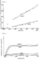
- Fig. 3 shows relations of those retardations.
- hatched areas denoted by A and B are areas corresponding to the above indicated relational expressions.
- Fig. 4 shows characteristics in the case of 1/200 duty multiplexing drive in typical display devices of the above indicated lots.
- the above description of the liquid crystal display device relates to the case of using only one phase plate and observing the front display surface perpendicularly thereto. However, if the display area increases, it happens frequently that the display surface is observed. obliquely. In consequence, it becomes necessary to lessen the dependency on the viewing cone.
- the length of a unit polymer projected on the liquid crystal layer differs dependent on whether the display device is observed in a direction normal to or inclined to the front surface. This difference appears as blurs in color compensation of the phase plate. Those irregularities can be prevented effectively by forming the phase plate 4 by a laminate body--of a plurality of sheets but it becomes difficult to handle the phase plate 4.
- the compensation can be made by the same principle as that in the conventional liquid crystal laminate body of two sheets; however, the optical axes change by steps as is different from the case of a twist nematic structure and accordingly the display is darkened and the contrast is lowered.
- phase plates are arranged on both sides of the liquid crystal layer, coloring caused by the change of the observing direction can be further suppressed.
- the projection direction of a unit polymer of the phase plate differs dependent on the upper or lower surface of the liquid crystal layer, influence of expansion or reduction of the projection range can be considerably reduced.
- the phase plate may be molded by a mixture of resin materials having different inherent birefringence factors or it may be formed by a laminate body of plates having different inherent birefringence factors.
- a combination of polycarbonate and polystylene is preferred. However, if a proportion of combination is inadequate, the birefringence of the resin is lost and, therefore, it is necessary to adjust the proportion of combination taking account of the stretching ratio.
- the phase plate may be formed by a laminate body of resin films having their optical axes intersecting orthogonally with each other.
- the phase plate in the above described example has its optical axis parallel to the main surface of the substrate and a resin material having its optical axis perpendicular to the surface of the substrate is placed on the above mentioned phase plate. According to this method, the expansion or reduction of the projection range of the unit polymer of the phase plate is offset dependent on the observing direction and the dependency on the viewing cone can be lessened.
- Fig. 5 shows characteristics of the dependency on the viewing cone in the case of a laminate body k formed by laminating a resin material of 110 ⁇ m in thickness having its optical axis perpendicular to the main surface of the substrate on a phase plate of 70 ⁇ m in thickness, as one of the above mentioned examples, in comparison with a single body j of a phase plate.
- the quality of display will be lowered unless the total thickness thereof is smaller than 500 ⁇ m.
- the present invention makes it possible to give a display with a non-colored beam (which enables a display of white color for the background) and a black color obtained by interception of the beam, in a manner in which the beam applied through birefringence rotary polarization in the liquid crystal panel is compensated as optical uniaxial substance.
- a display with a high quality can be represented as if black images are printed on white paper, and thus a high contrast is obtained. Since this display can be reversed from"black to white or vice versa, both a negative display and a positive display can be made.
- a color display can be given by using filters of three colors.
- the display device can be manufactured with good productivity at low cost and it can be made to have a large display area. Furthermore, since the entire body of the liquid crystal display device can be made thin, deviation in a display position or change in contrast due to parallax does not occur.
- a liquid crystal display device has a thin thickness and it is capable of representing black-and-white display and is suitable for high level multiplexing drive. Accordingly it can be utilized as a large-area display device of a dot matrix type or as a display of a word processor, a personal computer or the like. In addition, it can be also utilized as a color display in such a display device.
Abstract
Description
- The present invention relates to liquid crystal display devices which are suitable for high level multiplexing drive and the display of which is easy to see.
- Recently, field-effect type liquid crystal display devices having a twisted structure of liquid crystal molecules have been developed, which provide a wide range of high contrast (namely, a wide visual range) and enable high level multiplexing drive. In such liquid crystal display devices, liquid crystal molecules are oriented with a twist angle of 180° to 360° and a liquid crystal layer is placed between two polarizers. One of such liquid crystal display devices is disclosed for example in EPO-0131216 A3. In such a liquid crystal display device, the display color appears bluish or yellowish due to birefringence of the liquid crystal.
- On the other hand, if two liquid crystal panels are provided one upon another for phase compensation as disclosed for example in US Patent No. 4,443,065, the background color can be made close to white.
- The principle of this method will be briefly described. The hue observed due to birefringence of liquid crystal is an interference color, which appears because a beam is elliptically polarized in a liquid crystal layer. Consequently, an achromatic color can be obtained by twisting back the once twisted beam. For this purpose, a liquid crystal panel having the same characteristics as a liquid crystal panel used for drive is placed thereon, so as to be used for achromatization (compensation).
- However, since such liquid crystal panels include two liquid crystal cells placed one upon another, the entire body of the display device becomes thick, which unfavorably causes a shadow or remote-appearing image or a change in contrast due to parallax (dependent on the observing direction). Further, such liquid crystal panels have a large number of pixels because they are suited for high level multiplexing drive, and accordingly have a large display area. In addition, since the interference color depends also on the thickness of a liquid crystal layer, consequently, strict control is required for attaining evenness of the thickness of liquid crystal and stable characteristics over a wide area. As a result, the manufacturing efficiency is lowered and the manufacturing cost comes to be high.
- On the other hand, in order to adjust hue in a liquid crystal display device, the method of using a 1/4 wavelength plate or a phase plate is conventionally used as disclosed for example in US Patent No. 4,232,948 or Japanese Patent Laying-Open No. 600/1980. However, although coloring and achromatization are simply regarded as being based on opposite theories, it is practically difficult to effect achromatization by circular polarization or using a 1/4 wavelength plate. This is because a liquid crystal layer has complicated light transmitting characteristics although a wavelength plate (X plate) has effects on specified wavelengths of light. Further, it is difficult to adjust optical characteristics of the wavelengths plate and the liquid crystal layer since the quality of display is lowered if the liquid crystal layer does not have stable characteristics over a wide area. In consequence, phenomena such as appearance of other interference color, a darkened display or a lowered contrast occur, which unfavorably lowers the quality of display.
- There is proposed another technique which uses a uniaxially stretched film as polarized as used in a liquid crystal display device (as disclosed for example in Japanese Patent Laying-Open No. 192014/1988. According to this technique, since an interference color is liable to appear if a support film is attached to a polarizing film, the polarizing axis and the stretching direction are made to coincide in order to prevent interference and accordingly an already caused interference color of an optical body cannot be effaced.
- Therefore, a primary object of the present invention is to provide a liquid crystal display device which includes a liquid crystal cell having birefringence as described above and a thin phase plate placed on the liquid crystal cell with the optical axis of the phase plate intersecting with that of the liquid crystal cell. According to the present invention, retardation (Δn·d) of a liquid crystal layer is set to 600nm to 1000nm so as to enable color compensation in the liquid crystal display device which is suited for high level multiplexing drive and phase compensation is applied to an optical laminated body as an optical uniaxial substance. For the compensation, an optical uniaxial thin plate is used as the phase plate. Alternatively, an uniaxial stretched resin sheet is used as the phase plate. Thus, optical axis adjustment for the phase plate can be easily effected and it becomes easy to handle the phase plate. Consequently, productivity can be improved and a large-area display can be provided.
- Another feature of the present invention is that retardation of the phase plate is adjusted based on retardation of the liquid crystal layer. Thus, it becomes easy to adjust saturation, hue and the like and the quality of black-and-white display can be enhanced.
- A further feature of the present invention is that a pair of phase plates are arranged on both sides of the . liquid crystal layer. Alternatively, the phase plate is formed by materials having different inherent refractive factors. In a variant, the phase plate is formed by a plurality of laminated substances having optical axes intersecting orthogonally with each other. Thus, it becomes possible to suppress a shadow or remote-appearing image or a change in contrast due to parallax at the time of compensation for color interference of the liquid crystal layer.
- By making use of the achromatic display according to the present invention, it becomes possible to provide a large-area display or a color display.
- The foregoing and other objects, features, aspects and advantages of the present invention will become more apparent from the following detailed description of the present invention when taken in conjunction with the accompanying drawings.
-
- Fig. 1 is a sectional view of a liquid crystal display device according to an embodiment of the present invention.
- Fig. 2 is a graph showing a relation of retardation utilized in the principle of the present invention.
- Fig. 3 is a characteristic diagram showing a relation of retardation of a liquid crystal layer and a phase plate according to the present invention.
- Fig. 4 is a display characteristic diagram of a liquid crystal display device according to an embodiment of the present invention.
- Fig. 5 is a characteristic diagram related with viewing cones of some phase plates according to another embodiment of the present invention.
- A liquid crystal display device having a high contrast value and suited for high level multiplexing drive with a large duty ratio, among currently utilized field-effect type liquid crystal display devices, has a structure in which two polarizers hold therebetween a chiral nematic liquid crystal layer having a positive dielectric anisotropy, namely, a liquid crystal layer having a twisted structure of liquid crystal molecules with a twist angle of 180° to 300°.
- Fig. 1 shows a sectional view of a liquid crystal display device according to an embodiment of the invention, where the above described structure is adopted.
Substrates 1 are opposed to each other in this display device. Eachsubstrate 1 includes aglass plate 13 having an inner surface on whichtransparent electrodes 11 and anorientation film 12 of liquid crystal molecules are provided. Thetransparent electrodes 11 on one substrate are located perpendicularly to those on the other substrate so as to represent a dot matrix display for example. Eachorientation film 12 has been processed to homogenously orient liquid crystal molecules. Thosesubstrates 1 are laminated in parallel by usingsealing agents 5, to form a container. A chiral nematic phaseliquid crystal layer 2 having a positive dielectric anisotropy is interposed between thesubstrates 1. Thisliquid crystal layer 2 has a structure where liquid crystal molecules are twisted with a twist angle of 180° to 300° and, for example, it is a 240° twist nematic layer. Twopolarizers 3 are provided on respective outsides of thesubstrates 1 in a manner in which theliquid crystal layer 2 is held therebetween. Aphase plate 4 of resin having a thickness of less than 500µm is inserted between theliquid crystal layer 2 and one of the polarizers 3 (the upper one in the figure) with the optical axis of thephase plate 4 intersecting with the polarization axis of thepolarizer 3. - The characteristics of the
liquid crystal layer 2 will be more specifically described. If the twist angle of liquid crystal molecules becomes large as described above, the product of the birefringence anisotropy An and the thickness d of the liquid crystal layer, namely, the value of the retardation Δn·d (LC) has a direct effect on the quality of display and if a high-order interference occurs for example, color compensation cannot be effected by using the phase plate. More specifically, if the value An.d (LC) becomes smaller than 0.6, a light blue interference color appears and it is easy to compensate for the interference color. However, in that case, the transmissibility of the liquid crystal panel is considerably lowered and the display contrast value is deteriorated. Conversely, if the value Δn·d (LC) is larger than 1.0, the transmitted light becomes yellow and it is-difficult to effect color compensation by using thephase plate 4. If the value Δn·d (LC) becomes larger, a larger interference occurs and color control cannot be effected. Accordingly, the value Δn·d (LC) is preferably in the range of more than 0.55 and less than 1.2 and more preferably in the range of more than 0.6 and less than 1.0. - The above described
phase plate 4 can be formed by laminating sheets of uniaxially stretched polymeric resin materials such as polyvinyl butyrol, polyvinyl alcohol, polyester, cellulose acetate, cellulose butyrate, polyproylene, or polycarbonate. - The optical characteristics of the
liquid crystal layer 2 change dependent on presence or absence of an electric field so as to represent a display and if the laminated optical devices have a large thickness, a shadow or remote-appearing image or a change in contrast is liable to occur due to parallax. Since the phase plate has an optical uniaxial characteristic as is different from a conventional laminate of two liquid crystal panels, such phenomenon does not occur conspicuously. However, if the phase plate has a large thickness, such phenomenon can be observed. In order to suppress such phenomenon, it is desirable to set the thickness of theliquid crystal layer 2 smaller than 10µm, the value Δn·d (LC) in the range from 0.6 to 1.0 and the total thickness of thephase plate 4 smaller than 0.5mm and more preferably in the range from 25pm to 160µm. - The optical characteristics in the case of combining the liquid crystal layer and the phase plate will be described in more detail.
- The
liquid crystal layer 2 should have in principle the same conditions as those in a conventional display mode with a large twist angle of liquid crystal molecules utilizing birefringence (referred to hereinafter as a supper twisted (ST) mode). However, as a result of detailed examinations, it was found that theliquid crystal layer 2 exhibits complicated optical characteristics combined with optical characteristic due to the birefringence of the liquid crystal molecules and rotary polarization due to the twisted structure. - Therefore, in order to compensate for the interference color of the liquid crystal layer, the liquid crystal layer is made to be close to an optical uniaxial substance.
- This will be described with reference to Fig. 2. In general, in order to obtain a maximum contrast when a uniaxial substance is held by orthogonal Nicols, the polarization axis P of a polarizer is made to deviate by 45° from the optical axis S of the optical uniaxial substance as is well known.
- However, in the case of a liquid crystal layer, a rotary polarization occurs since liquid crystal molecules have a twisted structure (with a twist angle ϕ), and the optical axis rotates according to the twist direction. Thus, the above described condition cannot be obtained precisely.
- Taking those difficulties into consideration, the spectrum of transmitted light was examined by setting an angle β formed between the polarization axis of one polarizer and the orientation direction of liquid crystal molecules adjacent to the polarizer to 45° and rotating the other polarizer. As a result, it was found that there are two angles exhibiting transmitted light intensity characteristics corresponding to an optical uniaxial substance in the visible radiation range. It was found in those examinations that an angle a formed between the polarization axis P of the rotated polarizer and the axis L of the liquid crystal molecules adjacent thereto is approximately 45° or 1350 in the same direction as the twist direction of the liquid crystal molecules with respect to the axis of the liquid crystal molecules.
- Based on those conditions, examinations were carried out by using a polarizing microscope as to equivalence of a liquid crystal laminate body to an optical uniaxial substance. Fig. 2 shows the results of those examinations. More specifically, Fig. 2 shows optical characteristics which enables compensation for only rotary polarization caused by the twist structure. Based on those optical characteristics, the optical characteristics of the phase plate is adjusted so that the laminate body of the liquid crystal layer and the phase plate may be an optical uniaxial substance. Thus, according to Fig. 2, the color can be made achromatic by phase compensation with respect to an a column or b column, and in that case, a difference between heights of the a and b columns appears as a contrast.
- According to an experimental expression obtained based on the above described principle in a liquid crystal display device with a twist angle of 180° to 300° of liquid crystal molecules, if the retardation Δn·d (LC) of the liquid crystal layer and the retardation Δn·d (PH) is the phase plate satisfy the below relation (A):
- 0.6 x Δn·d (LC) +60 < Δn•d (PH) < 0.6 x Δn•d (LC) +210 (nm),
- compensation of a in Fig. 2 can be made and the basic mode in this case is a transmission type negative display mode.
- In the above described example, a high contrast value was exhibited when an angle 6 formed between the optical axis of the phase plate and the orientation direction of the liquid crystal molecules adjacent thereto was in the range from 70° to 110° and an angle β formed between the polarization axis of the polarizer and the orientation direction of the liquid crystal molecules adjacent thereto was in the range from 30° to 60°.
- Similarly, an experimental expression which enables compensation for b in Fig. 2 is represented as the below relation (B):
- (7.5 x 10⁻⁴) (Δn•d (LC) - 400)2 + 150 <Δn•d (PH)
- < (7.5 x 10⁻⁴) (Δn·d (LC) - 400)2 + 300 nm
- This relation (B) means, in comparison with the relation (A), that the phase plate utilized has an optical path difference smaller than that of the liquid crystal cell by about a 1/2 wavelength of the visible radiation range and the basic mode is a reflection type positive display mode.
- In either of the relations (A) and (B), reversal of negative and positive displays can be made if one of the polarizers is rotated by 90°. More specifically, the above described angles may be set with respect to either the polarization axis or the absorption axis of the polarizer.
- In order to suppress blurs in adjustment of the retardation Δn·d (LC) of the liquid crystal layer or temperature dependency, the angle 6 needs to deviate from 90° to either direction. More specifically, the angle δ is most preferably in the range from 70° to 88° or in the range from 92° to 110°.
- Typical examples according to the above described conditions are shown below.
-

-

- Fig. 3 shows relations of those retardations. Referring to Fig. 3, hatched areas denoted by A and B are areas corresponding to the above indicated relational expressions. Fig. 4 shows characteristics in the case of 1/200 duty multiplexing drive in typical display devices of the above indicated lots.
- The above description of the liquid crystal display device relates to the case of using only one phase plate and observing the front display surface perpendicularly thereto. However, if the display area increases, it happens frequently that the display surface is observed. obliquely. In consequence, it becomes necessary to lessen the dependency on the viewing cone.
- In the above described resin phase plate, it is considered that a large number of polymeric chains are arranged in one direction. Accordingly, the length of a unit polymer projected on the liquid crystal layer differs dependent on whether the display device is observed in a direction normal to or inclined to the front surface. This difference appears as blurs in color compensation of the phase plate. Those irregularities can be prevented effectively by forming the
phase plate 4 by a laminate body--of a plurality of sheets but it becomes difficult to handle thephase plate 4. For example, if the optical axes of the laminated sheets rotate a little from each other, the compensation can be made by the same principle as that in the conventional liquid crystal laminate body of two sheets; however, the optical axes change by steps as is different from the case of a twist nematic structure and accordingly the display is darkened and the contrast is lowered. - If a pair of phase plates are arranged on both sides of the liquid crystal layer, coloring caused by the change of the observing direction can be further suppressed. In this case, since the projection direction of a unit polymer of the phase plate differs dependent on the upper or lower surface of the liquid crystal layer, influence of expansion or reduction of the projection range can be considerably reduced.
- In addition, the phase plate may be molded by a mixture of resin materials having different inherent birefringence factors or it may be formed by a laminate body of plates having different inherent birefringence factors. For example, a combination of polycarbonate and polystylene is preferred. However, if a proportion of combination is inadequate, the birefringence of the resin is lost and, therefore, it is necessary to adjust the proportion of combination taking account of the stretching ratio.
- Further, the phase plate may be formed by a laminate body of resin films having their optical axes intersecting orthogonally with each other. For example, the phase plate in the above described example has its optical axis parallel to the main surface of the substrate and a resin material having its optical axis perpendicular to the surface of the substrate is placed on the above mentioned phase plate. According to this method, the expansion or reduction of the projection range of the unit polymer of the phase plate is offset dependent on the observing direction and the dependency on the viewing cone can be lessened.
- Fig. 5 shows characteristics of the dependency on the viewing cone in the case of a laminate body k formed by laminating a resin material of 110µm in thickness having its optical axis perpendicular to the main surface of the substrate on a phase plate of 70µm in thickness, as one of the above mentioned examples, in comparison with a single body j of a phase plate. The abscissa in Fig. 5 represents a viewing angle with respect to a line perpendicular to the display surface, in each of the cases of inclination toward the stretching direction of the phase plate (having the single body j∥, or the laminate body·k∥) and of inclination in a direction perpendicular to the stretching direction of the phase plate (having the single body j⊥, or the laminate body k⊥).
- Thus, even in the case of using multiple layers as the phase plate, the quality of display will be lowered unless the total thickness thereof is smaller than 500µm.
- As described in the foregoing, the present invention makes it possible to give a display with a non-colored beam (which enables a display of white color for the background) and a black color obtained by interception of the beam, in a manner in which the beam applied through birefringence rotary polarization in the liquid crystal panel is compensated as optical uniaxial substance. Thus, a display with a high quality can be represented as if black images are printed on white paper, and thus a high contrast is obtained. Since this display can be reversed from"black to white or vice versa, both a negative display and a positive display can be made. In addition, since the display is achromatic, a color display can be given by using filters of three colors.
- Since only one liquid crystal panel is used and the phase plate can be manufactured by molding, the display device can be manufactured with good productivity at low cost and it can be made to have a large display area. Furthermore, since the entire body of the liquid crystal display device can be made thin, deviation in a display position or change in contrast due to parallax does not occur.
- A liquid crystal display device according to the present invention has a thin thickness and it is capable of representing black-and-white display and is suitable for high level multiplexing drive. Accordingly it can be utilized as a large-area display device of a dot matrix type or as a display of a word processor, a personal computer or the like. In addition, it can be also utilized as a color display in such a display device.
Claims (7)
Δn·d (PH) of a birefringence anisotropy n and a thickness d of said phase plate satisfy a condition:
Applications Claiming Priority (7)
| Application Number | Priority Date | Filing Date | Title |
|---|---|---|---|
| JP1800088 | 1988-01-28 | ||
| JP18000/88 | 1988-01-28 | ||
| JP141293/88 | 1988-06-08 | ||
| JP14129388 | 1988-06-08 | ||
| JP280720/88 | 1988-11-07 | ||
| JP28072088 | 1988-11-07 | ||
| PCT/JP1989/000069 WO1989007282A1 (en) | 1988-01-28 | 1989-01-25 | Liquid crystal display |
Publications (3)
| Publication Number | Publication Date |
|---|---|
| EP0393191A1 true EP0393191A1 (en) | 1990-10-24 |
| EP0393191A4 EP0393191A4 (en) | 1990-12-05 |
| EP0393191B1 EP0393191B1 (en) | 1995-12-20 |
Family
ID=27282042
Family Applications (1)
| Application Number | Title | Priority Date | Filing Date |
|---|---|---|---|
| EP89901881A Expired - Lifetime EP0393191B1 (en) | 1988-01-28 | 1989-01-25 | Liquid crystal display |
Country Status (4)
| Country | Link |
|---|---|
| US (1) | US5119220A (en) |
| EP (1) | EP0393191B1 (en) |
| DE (1) | DE68925197T2 (en) |
| WO (1) | WO1989007282A1 (en) |
Cited By (7)
| Publication number | Priority date | Publication date | Assignee | Title |
|---|---|---|---|---|
| EP0367288A2 (en) * | 1988-11-04 | 1990-05-09 | Fuji Photo Film Co., Ltd. | Liquid crystal display |
| EP0382460A2 (en) * | 1989-02-06 | 1990-08-16 | Sharp Kabushiki Kaisha | Liquid crystal display device |
| EP0424951A1 (en) * | 1989-10-27 | 1991-05-02 | Fuji Photo Film Co., Ltd. | Liquid crystal display |
| EP0478779A1 (en) * | 1989-06-22 | 1992-04-08 | Citizen Watch Co. Ltd. | Liquid crystal display device and phase difference plates |
| EP0532292A1 (en) * | 1991-09-10 | 1993-03-17 | Sharp Kabushiki Kaisha | Liquid crystal display apparatus |
| EP0579247B1 (en) * | 1992-07-16 | 2000-06-14 | Seiko Epson Corporation | Liquid crystal electrooptical device |
| SG80517A1 (en) * | 1992-07-16 | 2001-05-22 | Seiko Epson Corp | Liquid crystal electrooptical device |
Families Citing this family (47)
| Publication number | Priority date | Publication date | Assignee | Title |
|---|---|---|---|---|
| WO1990011546A1 (en) * | 1989-03-28 | 1990-10-04 | Asahi Glass Company Ltd. | Liquid crystal display device |
| US5303075A (en) * | 1990-04-09 | 1994-04-12 | Seiko Epson Corporation | Liquid crystal display with phase difference plate having particular .DELTA.Δnxd at 45° angle to surface |
| JPH04294323A (en) * | 1991-03-25 | 1992-10-19 | Hitachi Ltd | Liquid crystal display device |
| US5245451A (en) * | 1991-09-27 | 1993-09-14 | Hughes Aircraft Company | Liquid crystal display method and apparatus with tuneable phase compensation |
| JP2916331B2 (en) * | 1991-11-08 | 1999-07-05 | 株式会社日立製作所 | Liquid crystal display |
| JPH05158016A (en) * | 1991-12-10 | 1993-06-25 | Sharp Corp | Liquid crystal display device |
| CN1035790C (en) * | 1993-02-02 | 1997-09-03 | 洛克威尔国际有限公司 | Compensator for liquid crystal oisplay |
| US5910854A (en) | 1993-02-26 | 1999-06-08 | Donnelly Corporation | Electrochromic polymeric solid films, manufacturing electrochromic devices using such solid films, and processes for making such solid films and devices |
| JP3144132B2 (en) * | 1993-03-22 | 2001-03-12 | 松下電器産業株式会社 | Liquid crystal display device and projection display device using the same |
| JPH0784252A (en) * | 1993-09-16 | 1995-03-31 | Sharp Corp | Liquid crystal display device |
| EP0649046B1 (en) * | 1993-10-19 | 2001-07-11 | Sharp Kabushiki Kaisha | A liquid crystal display device and a production method for the same |
| US5668663A (en) * | 1994-05-05 | 1997-09-16 | Donnelly Corporation | Electrochromic mirrors and devices |
| US6891563B2 (en) | 1996-05-22 | 2005-05-10 | Donnelly Corporation | Vehicular vision system |
| JPH09127521A (en) * | 1995-10-31 | 1997-05-16 | Sharp Corp | Display device with input function |
| US6067136A (en) * | 1997-07-23 | 2000-05-23 | Citizen Watch Co., Ltd. | Birefringence-type color liquid crystal display device |
| US6326613B1 (en) | 1998-01-07 | 2001-12-04 | Donnelly Corporation | Vehicle interior mirror assembly adapted for containing a rain sensor |
| US6172613B1 (en) | 1998-02-18 | 2001-01-09 | Donnelly Corporation | Rearview mirror assembly incorporating vehicle information display |
| US8294975B2 (en) | 1997-08-25 | 2012-10-23 | Donnelly Corporation | Automotive rearview mirror assembly |
| US6124886A (en) | 1997-08-25 | 2000-09-26 | Donnelly Corporation | Modular rearview mirror assembly |
| US6445287B1 (en) | 2000-02-28 | 2002-09-03 | Donnelly Corporation | Tire inflation assistance monitoring system |
| US8288711B2 (en) | 1998-01-07 | 2012-10-16 | Donnelly Corporation | Interior rearview mirror system with forwardly-viewing camera and a control |
| US6477464B2 (en) | 2000-03-09 | 2002-11-05 | Donnelly Corporation | Complete mirror-based global-positioning system (GPS) navigation solution |
| US6693517B2 (en) | 2000-04-21 | 2004-02-17 | Donnelly Corporation | Vehicle mirror assembly communicating wirelessly with vehicle accessories and occupants |
| US6329925B1 (en) | 1999-11-24 | 2001-12-11 | Donnelly Corporation | Rearview mirror assembly with added feature modular display |
| US6307607B1 (en) * | 1999-12-21 | 2001-10-23 | Philips Electronics North America Corporation | Reflective liquid crystal display with integrated compensation for skew angle rotation and birefringence effects |
| US7167796B2 (en) | 2000-03-09 | 2007-01-23 | Donnelly Corporation | Vehicle navigation system for use with a telematics system |
| US7370983B2 (en) | 2000-03-02 | 2008-05-13 | Donnelly Corporation | Interior mirror assembly with display |
| US7855755B2 (en) | 2005-11-01 | 2010-12-21 | Donnelly Corporation | Interior rearview mirror assembly with display |
| WO2001064481A2 (en) | 2000-03-02 | 2001-09-07 | Donnelly Corporation | Video mirror systems incorporating an accessory module |
| DE60220379T2 (en) | 2001-01-23 | 2008-01-24 | Donnelly Corp., Holland | IMPROVED VEHICLE LIGHTING SYSTEM |
| US7255451B2 (en) | 2002-09-20 | 2007-08-14 | Donnelly Corporation | Electro-optic mirror cell |
| US7581859B2 (en) | 2005-09-14 | 2009-09-01 | Donnelly Corp. | Display device for exterior rearview mirror |
| US6918674B2 (en) | 2002-05-03 | 2005-07-19 | Donnelly Corporation | Vehicle rearview mirror system |
| US7329013B2 (en) | 2002-06-06 | 2008-02-12 | Donnelly Corporation | Interior rearview mirror system with compass |
| EP1514246A4 (en) | 2002-06-06 | 2008-04-16 | Donnelly Corp | Interior rearview mirror system with compass |
| TWI259923B (en) * | 2002-08-01 | 2006-08-11 | Boe Hyids Technology Co Ltd | Liquid crystal display |
| US7310177B2 (en) | 2002-09-20 | 2007-12-18 | Donnelly Corporation | Electro-optic reflective element assembly |
| WO2004026633A2 (en) | 2002-09-20 | 2004-04-01 | Donnelly Corporation | Mirror reflective element assembly |
| WO2004103772A2 (en) | 2003-05-19 | 2004-12-02 | Donnelly Corporation | Mirror assembly for vehicle |
| US20040075790A1 (en) * | 2002-10-21 | 2004-04-22 | Wintek Corporation | Pellucid LCD and fabrication method of same |
| KR20050006175A (en) * | 2003-02-25 | 2005-01-15 | 도시바 마쯔시따 디스플레이 테크놀로지 컴퍼니, 리미티드 | Liquid crystal display element |
| JP4564795B2 (en) * | 2003-09-30 | 2010-10-20 | 株式会社日立製作所 | Liquid crystal display |
| US7446924B2 (en) | 2003-10-02 | 2008-11-04 | Donnelly Corporation | Mirror reflective element assembly including electronic component |
| US7308341B2 (en) | 2003-10-14 | 2007-12-11 | Donnelly Corporation | Vehicle communication system |
| US7626749B2 (en) | 2005-05-16 | 2009-12-01 | Donnelly Corporation | Vehicle mirror assembly with indicia at reflective element |
| US8154418B2 (en) | 2008-03-31 | 2012-04-10 | Magna Mirrors Of America, Inc. | Interior rearview mirror system |
| US9523860B2 (en) * | 2013-10-16 | 2016-12-20 | Emmett Dunham | Color-changing apparatus for active camouflage configurations |
Citations (3)
| Publication number | Priority date | Publication date | Assignee | Title |
|---|---|---|---|---|
| JPS539552A (en) * | 1976-07-13 | 1978-01-28 | Philips Nv | Information display unit |
| JPS56130703A (en) * | 1980-03-18 | 1981-10-13 | Toyobo Co Ltd | Quarter wavelength film |
| EP0246842A2 (en) * | 1986-05-19 | 1987-11-25 | Seiko Epson Corporation | A liquid crystal display device |
Family Cites Families (16)
| Publication number | Priority date | Publication date | Assignee | Title |
|---|---|---|---|---|
| DE2329618A1 (en) * | 1973-06-09 | 1975-01-02 | Fraunhofer Ges Forschung | ARRANGEMENT FOR MULTICOLORED DISPLAY, CONSISTING OF LIGHT SOURCE AND LINEAR POLARIZATION FILTER |
| US4019808A (en) * | 1973-06-09 | 1977-04-26 | Fraunhofer-Gesellschaft Zur Forderung Der Angewandten Forschung E.V. | Arrangement for a polychrome display |
| GB1469638A (en) * | 1973-07-18 | 1977-04-06 | Secr Defence | Liquid crystal display device |
| GB2028527B (en) * | 1978-06-08 | 1982-11-24 | American Liquid Xtal Chem | Liquid crystal displays |
| US4385806A (en) * | 1978-06-08 | 1983-05-31 | Fergason James L | Liquid crystal display with improved angle of view and response times |
| US4443065A (en) * | 1980-12-09 | 1984-04-17 | Sharp Kabushiki Kaisha | Interference color compensation double layered twisted nematic display |
| IN161652B (en) * | 1983-07-12 | 1988-01-09 | Bbc Brown Boveri & Cie | |
| GB2171549B (en) * | 1985-02-15 | 1988-05-18 | Citizen Watch Co Ltd | Liquid crystal display device |
| JPS61210324A (en) * | 1985-03-15 | 1986-09-18 | Hitachi Ltd | Liquid crystal display element |
| JPS6231822A (en) * | 1985-08-02 | 1987-02-10 | Hitachi Ltd | Liquid crystal displaying element |
| FR2595156B1 (en) * | 1986-02-28 | 1988-04-29 | Commissariat Energie Atomique | LIQUID CRYSTAL CELL USING ELECTRICALLY CONTROLLED BIREFRINGENCE EFFECT AND METHODS OF MANUFACTURING THE CELL AND A UNIAXIC NEGATIVE ANISOTROPY ANISOTROPY MEDIUM FOR USE THEREIN |
| JPS63192014A (en) * | 1987-02-04 | 1988-08-09 | Nitto Electric Ind Co Ltd | Substrate for liquid crystal cell |
| KR0134974B1 (en) * | 1987-07-29 | 1998-04-22 | 미다 가쓰시게 | Liquid crystal display device using nematic liquid crystal |
| US4984873A (en) * | 1987-08-31 | 1991-01-15 | Ricoh Company, Ltd. | Liquid crystal display device |
| JPH01120527A (en) * | 1987-11-04 | 1989-05-12 | Sharp Corp | Liquid crystal display device |
| US4936654A (en) * | 1988-01-28 | 1990-06-26 | Sanyo Electric Co., Ltd. | Liquid crystal display device |
-
1989
- 1989-01-25 DE DE68925197T patent/DE68925197T2/en not_active Expired - Lifetime
- 1989-01-25 US US07/381,631 patent/US5119220A/en not_active Expired - Lifetime
- 1989-01-25 WO PCT/JP1989/000069 patent/WO1989007282A1/en active IP Right Grant
- 1989-01-25 EP EP89901881A patent/EP0393191B1/en not_active Expired - Lifetime
Patent Citations (3)
| Publication number | Priority date | Publication date | Assignee | Title |
|---|---|---|---|---|
| JPS539552A (en) * | 1976-07-13 | 1978-01-28 | Philips Nv | Information display unit |
| JPS56130703A (en) * | 1980-03-18 | 1981-10-13 | Toyobo Co Ltd | Quarter wavelength film |
| EP0246842A2 (en) * | 1986-05-19 | 1987-11-25 | Seiko Epson Corporation | A liquid crystal display device |
Non-Patent Citations (1)
| Title |
|---|
| See also references of WO8907282A1 * |
Cited By (12)
| Publication number | Priority date | Publication date | Assignee | Title |
|---|---|---|---|---|
| EP0367288A2 (en) * | 1988-11-04 | 1990-05-09 | Fuji Photo Film Co., Ltd. | Liquid crystal display |
| EP0367288A3 (en) * | 1988-11-04 | 1991-05-02 | Fuji Photo Film Co., Ltd. | Liquid crystal display |
| US5189538A (en) * | 1988-11-04 | 1993-02-23 | Fuji Photo Film Co., Ltd. | Liquid crystal display having positive and negative birefringent compensator films |
| EP0382460A2 (en) * | 1989-02-06 | 1990-08-16 | Sharp Kabushiki Kaisha | Liquid crystal display device |
| EP0382460A3 (en) * | 1989-02-06 | 1991-11-06 | Sharp Kabushiki Kaisha | Liquid crystal display device |
| EP0478779A1 (en) * | 1989-06-22 | 1992-04-08 | Citizen Watch Co. Ltd. | Liquid crystal display device and phase difference plates |
| EP0478779A4 (en) * | 1989-06-22 | 1992-07-01 | Citizen Watch Co. Ltd. | Liquid crystal display device and phase difference plates |
| EP0424951A1 (en) * | 1989-10-27 | 1991-05-02 | Fuji Photo Film Co., Ltd. | Liquid crystal display |
| US5138474A (en) * | 1989-10-27 | 1992-08-11 | Fuji Photo Film Co., Ltd. | Liquid crystal display with compensator having two films with positive and negative intrinsic birefringence, respectively |
| EP0532292A1 (en) * | 1991-09-10 | 1993-03-17 | Sharp Kabushiki Kaisha | Liquid crystal display apparatus |
| EP0579247B1 (en) * | 1992-07-16 | 2000-06-14 | Seiko Epson Corporation | Liquid crystal electrooptical device |
| SG80517A1 (en) * | 1992-07-16 | 2001-05-22 | Seiko Epson Corp | Liquid crystal electrooptical device |
Also Published As
| Publication number | Publication date |
|---|---|
| EP0393191B1 (en) | 1995-12-20 |
| US5119220A (en) | 1992-06-02 |
| DE68925197D1 (en) | 1996-02-01 |
| DE68925197T2 (en) | 1996-07-18 |
| WO1989007282A1 (en) | 1989-08-10 |
| EP0393191A4 (en) | 1990-12-05 |
Similar Documents
| Publication | Publication Date | Title |
|---|---|---|
| EP0393191B1 (en) | Liquid crystal display | |
| EP0512459B1 (en) | Liquid crystal display device | |
| CN100381906C (en) | In-plane switching liquid crystal display comprising compensation film for angular field of view using +A-plate and +C-plate | |
| EP2251736A1 (en) | Liquid crystal display device | |
| US4936654A (en) | Liquid crystal display device | |
| US4906073A (en) | Liquid crystal display device using nematic liquid crystal having twisted helical structure and a phase correction plate | |
| JP2003195310A (en) | Active matrix type liquid crystal display device | |
| JP3289386B2 (en) | Color liquid crystal display | |
| EP0886170B1 (en) | Liquid crystal display device | |
| JP3070181B2 (en) | Liquid crystal display | |
| JPH0815691A (en) | Color liquid crystal display device | |
| JPH03116015A (en) | Liquid crystal display element | |
| JP3774575B2 (en) | Reflective liquid crystal display | |
| JP3289385B2 (en) | Color liquid crystal display | |
| JP2555176B2 (en) | Liquid crystal display | |
| JP3052864B2 (en) | Liquid crystal display | |
| JP2849025B2 (en) | Liquid crystal display | |
| JP2627311B2 (en) | LCD display | |
| JP3006155B2 (en) | Liquid crystal display | |
| JPH08190081A (en) | Color liquid crystal display element | |
| JPH03155521A (en) | Liquid crystal display | |
| JP3058971B2 (en) | Liquid crystal display device | |
| JPH11174497A (en) | Color liquid crystal display device | |
| JPH03116024A (en) | Liquid crystal display element | |
| JPH0243515A (en) | Optical compensating liquid crystal display element |
Legal Events
| Date | Code | Title | Description |
|---|---|---|---|
| PUAI | Public reference made under article 153(3) epc to a published international application that has entered the european phase |
Free format text: ORIGINAL CODE: 0009012 |
|
| 17P | Request for examination filed |
Effective date: 19890721 |
|
| AK | Designated contracting states |
Kind code of ref document: A1 Designated state(s): CH DE GB LI |
|
| A4 | Supplementary search report drawn up and despatched |
Effective date: 19901018 |
|
| AK | Designated contracting states |
Kind code of ref document: A4 Designated state(s): CH DE GB LI |
|
| 17Q | First examination report despatched |
Effective date: 19921019 |
|
| GRAA | (expected) grant |
Free format text: ORIGINAL CODE: 0009210 |
|
| AK | Designated contracting states |
Kind code of ref document: B1 Designated state(s): CH DE GB LI |
|
| REF | Corresponds to: |
Ref document number: 68925197 Country of ref document: DE Date of ref document: 19960201 |
|
| REG | Reference to a national code |
Ref country code: CH Ref legal event code: NV Representative=s name: HEPP, WENGER & RYFFEL AG |
|
| PLBE | No opposition filed within time limit |
Free format text: ORIGINAL CODE: 0009261 |
|
| STAA | Information on the status of an ep patent application or granted ep patent |
Free format text: STATUS: NO OPPOSITION FILED WITHIN TIME LIMIT |
|
| 26N | No opposition filed | ||
| REG | Reference to a national code |
Ref country code: GB Ref legal event code: IF02 |
|
| PGFP | Annual fee paid to national office [announced via postgrant information from national office to epo] |
Ref country code: CH Payment date: 20080116 Year of fee payment: 20 |
|
| PGFP | Annual fee paid to national office [announced via postgrant information from national office to epo] |
Ref country code: GB Payment date: 20080123 Year of fee payment: 20 Ref country code: DE Payment date: 20080117 Year of fee payment: 20 |
|
| REG | Reference to a national code |
Ref country code: CH Ref legal event code: PL |
|
| REG | Reference to a national code |
Ref country code: GB Ref legal event code: PE20 Expiry date: 20090124 |
|
| PG25 | Lapsed in a contracting state [announced via postgrant information from national office to epo] |
Ref country code: GB Free format text: LAPSE BECAUSE OF EXPIRATION OF PROTECTION Effective date: 20090124 |