EP0397196A2 - Data communication bypass apparatus and method - Google Patents
Data communication bypass apparatus and method Download PDFInfo
- Publication number
- EP0397196A2 EP0397196A2 EP90108916A EP90108916A EP0397196A2 EP 0397196 A2 EP0397196 A2 EP 0397196A2 EP 90108916 A EP90108916 A EP 90108916A EP 90108916 A EP90108916 A EP 90108916A EP 0397196 A2 EP0397196 A2 EP 0397196A2
- Authority
- EP
- European Patent Office
- Prior art keywords
- network controller
- low speed
- high speed
- time slot
- channels
- Prior art date
- Legal status (The legal status is an assumption and is not a legal conclusion. Google has not performed a legal analysis and makes no representation as to the accuracy of the status listed.)
- Granted
Links
- 238000004891 communication Methods 0.000 title claims abstract description 41
- 238000000034 method Methods 0.000 title claims description 12
- 230000003287 optical effect Effects 0.000 claims abstract description 14
- 230000001360 synchronised effect Effects 0.000 claims abstract description 12
- 238000012544 monitoring process Methods 0.000 claims description 6
- 238000001514 detection method Methods 0.000 claims 6
- 238000010586 diagram Methods 0.000 description 6
- 239000000835 fiber Substances 0.000 description 5
- 102100040338 Ubiquitin-associated and SH3 domain-containing protein B Human genes 0.000 description 4
- 101710143616 Ubiquitin-associated and SH3 domain-containing protein B Proteins 0.000 description 4
- 230000005540 biological transmission Effects 0.000 description 3
- 230000006870 function Effects 0.000 description 2
- 238000012423 maintenance Methods 0.000 description 2
- 230000037361 pathway Effects 0.000 description 2
- 238000012546 transfer Methods 0.000 description 2
- 238000006243 chemical reaction Methods 0.000 description 1
- 230000000694 effects Effects 0.000 description 1
- 230000007257 malfunction Effects 0.000 description 1
- 230000000737 periodic effect Effects 0.000 description 1
- 230000002093 peripheral effect Effects 0.000 description 1
Images


Classifications
-
- H—ELECTRICITY
- H04—ELECTRIC COMMUNICATION TECHNIQUE
- H04J—MULTIPLEX COMMUNICATION
- H04J3/00—Time-division multiplex systems
- H04J3/02—Details
- H04J3/08—Intermediate station arrangements, e.g. for branching, for tapping-off
-
- H—ELECTRICITY
- H04—ELECTRIC COMMUNICATION TECHNIQUE
- H04J—MULTIPLEX COMMUNICATION
- H04J3/00—Time-division multiplex systems
- H04J3/02—Details
- H04J3/14—Monitoring arrangements
-
- H—ELECTRICITY
- H04—ELECTRIC COMMUNICATION TECHNIQUE
- H04J—MULTIPLEX COMMUNICATION
- H04J2203/00—Aspects of optical multiplex systems other than those covered by H04J14/05 and H04J14/07
- H04J2203/0001—Provisions for broadband connections in integrated services digital network using frames of the Optical Transport Network [OTN] or using synchronous transfer mode [STM], e.g. SONET, SDH
- H04J2203/0057—Operations, administration and maintenance [OAM]
- H04J2203/006—Fault tolerance and recovery
Definitions
- the present invention relates to bypass apparatus so as to route data communication channels through an add/drop multiplexer (ADM) if the associated ADM controller is not operating properly.
- ADM add/drop multiplexer
- the apparatus and methodology is particularly directed to telephony, but is applicable in other situations where bypass routing of information is desirable when a non-redundant component is sensed as not operating properly.
- the present invention is directed to a device and associated method for bypassing the control of a non-redundant module, such as a network controller, when that module is sensed to be operating improperly.
- ADM's add/drop multiplexers
- the add/drop multiplexer may be associated with high speed east and west ports (the terms "east” and "west” are commonly used in telephony with respect to describing communication direction) associated with a high speed channel operating at 51.84 megabits per second.
- This high speed channel may conform to the synchronous optical network (SONET) standard for use in fiber optics interfaces or may conform to such a standard with an electrical interface.
- SONET synchronous optical network
- the add/drop multiplexer further comprises a plurality of lower speed channels such as channels conforming to the DS-1 standard; that is channels (also called links), operating at 1.544 megabits per second.
- Each DS-1 channel can further comprise up to 24 lower speed channels such as 64 kilobit per second DS-0 channels so that in effect, the high speed channel multiplexes the DS-1 channels which in turn multiplex lower speed DS-0 channels.
- the add/drop multiplexer is therefore particularly designed to add or remove DS-1 channels from the high speed channel and to pass these channels along with other through channels via the high speed channel downstream.
- Such add/drop multiplexers typically incorporate a network element controller which provides performance monitoring, control, alarm reporting, and provisioning of the network element.
- the network element controller is responsible for provisioning the time slot multiplexer which in turn provides the ability to crossconnect any synchronous transport signal (STS) virtual tributary (VT) as well as any DS-1 add/drop link.
- STS synchronous transport signal
- VT virtual tributary
- the network element controller is not of a redundant type, its failure would prevent the proper passage of data communication information between the east and west interfaces of the add/drop multiplexer. It is especially desirable that if the network controller fails, that the SONET section data communication channel information pass through the ADM and thus avoid the network controller.
- the craft orderwire alarm module (COA) of the present invention include circuitry which can detect the status of a watchdog timer which in turn monitors the performance of a network controller. Upon timeout of the watchdog timer, the COA reprovisions the ADM's time slot multiplexer so that the section datacom channel is connected through the east-west high speed interfaces. The watchdog timer also disables the microprocessor associated with the network controller so as to prevent its interference with the TSM.
- COA craft orderwire alarm module
- No prior art device which allows use of a non-redundant network controller in association with an add/drop multiplexer so as to allow specified channels within the high speed channel (such as section data communication information) to be passed through the ADM upon perceived failure of the network controller.
- the present invention is directed to a data communication bypass apparatus particularly for use in conjunction with an add/drop multiplexer (ADM).
- ADM add/drop multiplexer
- the ADM of the present invention incorporates a non-redundant single network controller (SNC), an associated craft, orderwire alarm module (COA) and a time slot multiplexer (TSM) for use in adding or dropping low speed channels from a high speed channel.
- SNC non-redundant single network controller
- COA orderwire alarm module
- TSM time slot multiplexer
- the high speed channel associated with the present invention conforms to the SONET communication standard (American National Standard for Telecommunication -ANSI- standard T1.105-1988).
- This particular standard incorporates section overhead bytes forming part of the synchronous transport signal (STS) including a section data communication channel comprising three bytes; namely, bytes D1, D2, and D3.
- STS synchronous transport signal
- This section data communication channel is a 192 kilobits per second message channel particularly directed to communicating
- the network controller receives from the high speed interface information concerning the data packets so as to terminate or forward data packets downstream, depending upon perceived conditions. If the network controller (SNC) fails, it is desirable to bypass the SNC and route the data communication channel comprising the D1, D2, and D3 bytes from the east high speed interface via the time slot multiplexer to the west high speed interface.
- SNC network controller
- the section data communication channel is routed from the east high speed interface to the network controller.
- the network controller receives the data packets, terminates the data packets for that site, and forwards the remaining packets via the DS-1 channels to the appropriate add/drop multiplexer.
- the present invention incorporates a watchdog timer and a reprovisioning module within the craft orderwire alarm (COA).
- the watchdog timer monitors the performance of the SNC. If it senses an SNC failure, it informs the COA which then reprovisions the TSM so that the section data communication channel is routed through the TSM to the west high speed interface channel. In other words, the COA re-configures the TSM so as to bypass the SNC.
- ADM add/drop multiplexer
- Another object of the present invention is to provide a channel routing mechanism incorporating a craft orderwire alarm which monitors a watchdog timer so as to reprovision an associated time slot multiplexer to reroute designated low speed channels to a downstream interface when a non-redundant network controller is perceived to be operating improperly.
- Figure 1 illustrates various devices 20, 22 and 24, that can interface with an optical carrier (fiber optic) transmission medium such as the optical carrier medium 42, 44 operating within the Synchronous Optical Network (SONET) standard adopted by the American National Standards Institute, Inc. (ANSI) as set forth in their standard No. TI.105-1988 entitled "Digital Hierarchy Optical Interface Rates and Formats Specification".
- SONET Synchronous Optical Network
- ANSI American National Standards Institute, Inc.
- STS Synchronous Transport Signal
- the STS-1 (STS level 1) is defined as the basic building block signal with a transfer rate of 51.840 megabits per second (Mbit/s).
- Mbit/s megabits per second
- an STS-N optical carrier level is simply the level 1 rate multiplied by N, where N is an integer equal to or greater than one.
- the STS bit stream is presented in a frame where the STS-1 frame comprises 810 bytes which can be visualized as nine rows, each 90 bytes wide (see Figure 5), with the frame period equal to 125 microseconds.
- the first three columns comprise what is called transport overhead, which in turn comprises section and line overhead. Section overhead deals with the SONET section layer which is directed to the transport of STS-N frames across the physical medium.
- the line overhead deals with the line layer which is directed to the transport of Path layer payload.
- the payload is a synchronous payload whose envelope can reside across two STS-N envelopes.
- the synchronous payload envelope (SPE) consists of nine rows, each 87 columns wide. The first column contains path overhead leaving 774 bytes available for payload. It is within this payload that channels of telephonic information are contained, these channels conforming to various digital signal standards such as DS-0 (64 kbits/s), DS-1 (1.544 mbits/s) and DS-3 (44.736 mbits/s).
- the fiber transmission system (FTS) 20 is interconnected between an OC-3 carrier 44 operating at 155.52 megabits per second and an electrical DS-3 standard medium 41 operating at 44.736 megabits per second.
- the fiber transmission system can also connect to a 55.84 megabits per second electrical interface medium 43 identified as STSX-1. This interface is an electrical implementation of the synchronized optical network interface (SONET).
- SONET synchronized optical network interface
- the terminal multiplexer (TM) 22 has a high speed port 28 operating at 51.84 mbits/s that can be equipped with either an electrical interface (STSX-1 electrical path) or a fiber optic interface for operation with the OC-1 SONET Standard.
- the low speed port 30 of the terminal multiplexer is interfaced with a DSX-1 electrical telephony standard operating at 1.544 megabits per second.
- Each DS-1 interface can incorporate up to 24 DS-0 channels each operating at 64 kilobits per second.
- the terminal multiplexer therefor interfaces from 1 - 28 DS1 channels with one OC-1 or one STSX-1 carrier.
- the add/drop multiplexer (ADM) 24 is functionally identical to the terminal multiplexer except that the ADM is equipped with east and west high speed interface media 32 and 34, respectively.
- the low speed port 38 is similar in operation to the low speed port 30 associated with the terminal multiplexer.
- Section overhead Within the section overhead are three bytes, D1, D2 and D3, known as the section data communication channel. These three bytes are allocated to section data communications and are considered by the SONET standard to be one 192 kbit/s message based channel for purposes of conveying alarm, maintenance, control, monitor, administration and other communication needs between section terminating equipment.
- Section terminating equipment include add/drop multiplexers and terminal multiplexers.
- the preferred embodiment of the present invention is directed to the transfer of section data communication information, it also is applicable to other channels such as the line data communication channel comprising bytes D4 through D12 (see Figure 6).
- the present invention could be used to convey any data in the high speed communication channel through the ADM if such bypassing is desired.
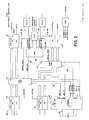
- FIG. 2 illustrates the overall modules comprising ADM 24.
- the ADM comprises an east high speed interface 26 connected to media 32, a west high speed interface 28 connected to media 34, a time slot multiplexer 52, a craft orderwire alarm (COA) 50, a non-redundant network controller (SNC) 56, a clock 30 and a digital signal-1 (DS-1) interface 58.
- COA craft orderwire alarm
- SNC non-redundant network controller
- DS-1 interface 58 digital signal-1 interface 58.
- the east and west high speed interfaces, the TSM, and the DS-1 interface are redundant in that two pathways are provided; namely, path A and path B which are commonly used in telecommunications to increase reliability.
- the craft orderwire alarm unit 50 is responsible for determining whether path A or path B is to be utilized along with the associated modules, depending upon perceived conditions.
- the network controller (SNC 56) is not redundant primarily due to the normal high reliability of this controller as well as due to the use of the present invention as described more fully below which achieves the purpose of redundancy; namely to maintain specific datacommunications, even if the network controller becomes faulty.
- the east high speed interface 26 receives the high speed data from the optical carrier medium (see Figure 1) and directs the information to the time slot multiplexer (TSM) 52.
- TSM time slot multiplexer
- the purpose of the time slot multiplexer is to provide cross-connections between any virtual tributary within the high speed data channel to any DS-1 add/drop link 32.
- the virtual tributary is the SONET structure for the transport of sub-STS-1 payload, such as DS-1, DS-1C and DS-2 digital signal channels.
- the TSM includes a microprocessor 42 which is used to provision the cross-connect function of the TSM by changing data within the connect memory of the TSM.
- the TSM connect memory in turn controls the east and west interface connections.
- the network controller 56 is therefore responsible for provisioning the TSM so as to provide interconnections between the input data bus 36 and the output data bus 38.
- This controller connects to an asynchronous serial bus 61 that operates at a data rate of 128 kbit/s with associated start and stop bits via a multiprocessor serial interface 51.
- the serial bus protocol is based upon the Intel Corporation (Santa Clara, CA) Micro Controller Mode 2 operation and comprises a start bit, eight data bits, a program bit and a stop bit.
- the controller is presented with data via a serial bus 34 to an input/output module 40 which in turn is connected to microprocessor 42.
- the data is then acted upon and presented to a second input/output module 44 and transferred back to the time slot interchanger via serial bus 35.
- a watchdog timer 46 which monitors the performance of the microprocessor to insure that it is operating properly.
- the status of the watchdog timer is presented to a gate module 48 which is connected via status lines 46 to the COA 50.
- the microprocessor 42 When the network controller is operating properly, the microprocessor 42 presents information onto the multiprocessor serial interface 51 which is connected to a second microprocessor serial interface 53 associated with the TSM 52.
- the data received by the microprocessor serial interface 53 controls the provisioning of the connect memory forming part of the TSM which effectively directs the pathway between incoming data via bus 36 to outgoing data via bus 38. This is shown in phantom by line 55.
- the SNC receives the data communication channel information and terminates it if it is appropriate for this particular ADM or forwards the information downstream via the TSM to the west high speed interface.
- the watchdog timer 46 is an interval timer which is used to detect possible malfunction of the SNC and thus provides a sanity check for the microprocessor and its firmware. In operation, the watchdog timer must be reset by the microprocessor software on a periodic basis to insure that the processor is executing its associated program code correctly. If the processor does not reset the timer within its time-out period, the watchdog timer will expire. The expiration of the watchdog timer isolates the microprocessor from the system peripherals. Thus upon timeout, the watchdog timer forces the resetting of microprocessor 42 via a signal on output line 47.
- the timeout of the watchdog timer 46 also causes status alarm information via bus 49 to be conveyed to the COA.
- the COA via its multiprocessor serial interface 62 causes the connect memory of the TSM with regard to the data communication channel to be reprovisioned so as to effectively connect the incoming data channel via bus 36 to the west high speed interface bus 38.
- This is shown diagrammatically in Figure 4 by the repositioning of arrows 63 and 64 from the connections to the serial busses 33 and 35 to the through connection 65.
- Figure 4 also shows the effective disconnection of the serial busses between the TSM and the SNC.
- the same apparatus can be used to reprovision any desired low speed channel within the SONET STS or the other high speed communication channel which is interconnected to an ADM.
- the present invention is applicable to bypassing any low speed channel comprising part of the high speed channel information transferred from the east high speed interface to the west high speed interface.
Abstract
Description
- The present invention relates to bypass apparatus so as to route data communication channels through an add/drop multiplexer (ADM) if the associated ADM controller is not operating properly. The apparatus and methodology is particularly directed to telephony, but is applicable in other situations where bypass routing of information is desirable when a non-redundant component is sensed as not operating properly.
- The present invention is directed to a device and associated method for bypassing the control of a non-redundant module, such as a network controller, when that module is sensed to be operating improperly. Recently, telephony has begun to use what are known as add/drop multiplexers (ADM's) whose function is to add or remove telephony channels from a high speed multiplexed telephony communication highway. For example, the add/drop multiplexer may be associated with high speed east and west ports (the terms "east" and "west" are commonly used in telephony with respect to describing communication direction) associated with a high speed channel operating at 51.84 megabits per second. This high speed channel may conform to the synchronous optical network (SONET) standard for use in fiber optics interfaces or may conform to such a standard with an electrical interface.
- In either event, the add/drop multiplexer further comprises a plurality of lower speed channels such as channels conforming to the DS-1 standard; that is channels (also called links), operating at 1.544 megabits per second. Each DS-1 channel can further comprise up to 24 lower speed channels such as 64 kilobit per second DS-0 channels so that in effect, the high speed channel multiplexes the DS-1 channels which in turn multiplex lower speed DS-0 channels.
- The add/drop multiplexer is therefore particularly designed to add or remove DS-1 channels from the high speed channel and to pass these channels along with other through channels via the high speed channel downstream. Such add/drop multiplexers typically incorporate a network element controller which provides performance monitoring, control, alarm reporting, and provisioning of the network element. In particular, the network element controller is responsible for provisioning the time slot multiplexer which in turn provides the ability to crossconnect any synchronous transport signal (STS) virtual tributary (VT) as well as any DS-1 add/drop link. If the network element controller is not of a redundant type, its failure would prevent the proper passage of data communication information between the east and west interfaces of the add/drop multiplexer. It is especially desirable that if the network controller fails, that the SONET section data communication channel information pass through the ADM and thus avoid the network controller.
- In particular, the craft orderwire alarm module (COA) of the present invention include circuitry which can detect the status of a watchdog timer which in turn monitors the performance of a network controller. Upon timeout of the watchdog timer, the COA reprovisions the ADM's time slot multiplexer so that the section datacom channel is connected through the east-west high speed interfaces. The watchdog timer also disables the microprocessor associated with the network controller so as to prevent its interference with the TSM.
- No prior art device is known which allows use of a non-redundant network controller in association with an add/drop multiplexer so as to allow specified channels within the high speed channel (such as section data communication information) to be passed through the ADM upon perceived failure of the network controller.
- The present invention is directed to a data communication bypass apparatus particularly for use in conjunction with an add/drop multiplexer (ADM). The ADM of the present invention incorporates a non-redundant single network controller (SNC), an associated craft, orderwire alarm module (COA) and a time slot multiplexer (TSM) for use in adding or dropping low speed channels from a high speed channel. The high speed channel associated with the present invention conforms to the SONET communication standard (American National Standard for Telecommunication -ANSI- standard T1.105-1988). This particular standard incorporates section overhead bytes forming part of the synchronous transport signal (STS) including a section data communication channel comprising three bytes; namely, bytes D1, D2, and D3. This section data communication channel is a 192 kilobits per second message channel particularly directed to communicating information concerning alarms, maintenance, control, monitor, administration and other communication needs between section terminating equipment as defined in the SONET standard.
- Normally the network controller receives from the high speed interface information concerning the data packets so as to terminate or forward data packets downstream, depending upon perceived conditions. If the network controller (SNC) fails, it is desirable to bypass the SNC and route the data communication channel comprising the D1, D2, and D3 bytes from the east high speed interface via the time slot multiplexer to the west high speed interface.
- Typically at any given ADM. location, the section data communication channel is routed from the east high speed interface to the network controller. The network controller receives the data packets, terminates the data packets for that site, and forwards the remaining packets via the DS-1 channels to the appropriate add/drop multiplexer.
- The present invention incorporates a watchdog timer and a reprovisioning module within the craft orderwire alarm (COA). The watchdog timer monitors the performance of the SNC. If it senses an SNC failure, it informs the COA which then reprovisions the TSM so that the section data communication channel is routed through the TSM to the west high speed interface channel. In other words, the COA re-configures the TSM so as to bypass the SNC.
- It is therefore a principal object of the present invention to provide a channel routing mechanism for passing designated low speed channels through an add/drop multiplexer (ADM) if a non-redundant network controller is perceived to be operating improperly.
- Another object of the present invention is to provide a channel routing mechanism incorporating a craft orderwire alarm which monitors a watchdog timer so as to reprovision an associated time slot multiplexer to reroute designated low speed channels to a downstream interface when a non-redundant network controller is perceived to be operating improperly..
- Other objects of the present invention will in part be obvious and in part will appear hereinafter.
- For a fuller understanding of the nature and objects of the present invention, reference should be made to the following detailed description taken in connection with the accompanying drawings, in which:
- Figure 1 is an overall block diagram of a synchronous optical transport system showing use of an add/drop multiplexer which can incorporate a data communication bypass mechanism according to the present invention.
- Figure 2 is a block diagram of an add/drop multiplexer shown in Figure 1.
- Figure 3 is a detailed block diagram of the east high speed interface, west high speed interface, time slot multiplexer, non-redundant network controller, and craft orderwire alarm modules shown in Figure 2 indicating the data path for the data communication channel received from the east high speed interface when the network controller is operating properly.
- Figure 4 is a detailed block diagram of the same modules shown in Figure 3 indicating the communication path for the data communication channel when the non-redundant controller is operating improperly.
- Figure 5 is a diagram showing the frame format for an asynchronous transport signal frame, specifically an STS-1 frame illustrating both transport overhead and envelope capacity.
- Figure 6 is a diagram of the overhead byte locations in an STS-1 frame.
- Figure 1 illustrates
various devices optical carrier medium level 1 rate multiplied by N, where N is an integer equal to or greater than one. The STS bit stream is presented in a frame where the STS-1 frame comprises 810 bytes which can be visualized as nine rows, each 90 bytes wide (see Figure 5), with the frame period equal to 125 microseconds. The first three columns comprise what is called transport overhead, which in turn comprises section and line overhead. Section overhead deals with the SONET section layer which is directed to the transport of STS-N frames across the physical medium. - The line overhead deals with the line layer which is directed to the transport of Path layer payload. The payload is a synchronous payload whose envelope can reside across two STS-N envelopes.
- The synchronous payload envelope (SPE) consists of nine rows, each 87 columns wide. The first column contains path overhead leaving 774 bytes available for payload. It is within this payload that channels of telephonic information are contained, these channels conforming to various digital signal standards such as DS-0 (64 kbits/s), DS-1 (1.544 mbits/s) and DS-3 (44.736 mbits/s).
- The fiber transmission system (FTS) 20 is interconnected between an OC-3
carrier 44 operating at 155.52 megabits per second and an electrical DS-3standard medium 41 operating at 44.736 megabits per second. The fiber transmission system can also connect to a 55.84 megabits per secondelectrical interface medium 43 identified as STSX-1. This interface is an electrical implementation of the synchronized optical network interface (SONET). - The terminal multiplexer (TM) 22 has a
high speed port 28 operating at 51.84 mbits/s that can be equipped with either an electrical interface (STSX-1 electrical path) or a fiber optic interface for operation with the OC-1 SONET Standard. Thelow speed port 30 of the terminal multiplexer is interfaced with a DSX-1 electrical telephony standard operating at 1.544 megabits per second. Each DS-1 interface can incorporate up to 24 DS-0 channels each operating at 64 kilobits per second. The terminal multiplexer therefor interfaces from 1 - 28 DS1 channels with one OC-1 or one STSX-1 carrier. - The add/drop multiplexer (ADM) 24 is functionally identical to the terminal multiplexer except that the ADM is equipped with east and west high
speed interface media low speed port 38 is similar in operation to thelow speed port 30 associated with the terminal multiplexer. - Within the section overhead are three bytes, D1, D2 and D3, known as the section data communication channel. These three bytes are allocated to section data communications and are considered by the SONET standard to be one 192 kbit/s message based channel for purposes of conveying alarm, maintenance, control, monitor, administration and other communication needs between section terminating equipment. Section terminating equipment include add/drop multiplexers and terminal multiplexers.
- Although the preferred embodiment of the present invention is directed to the transfer of section data communication information, it also is applicable to other channels such as the line data communication channel comprising bytes D4 through D12 (see Figure 6). In fact the present invention could be used to convey any data in the high speed communication channel through the ADM if such bypassing is desired.
- More particularly, Figure 2 illustrates the overall
modules comprising ADM 24. The ADM comprises an easthigh speed interface 26 connected tomedia 32, a westhigh speed interface 28 connected tomedia 34, atime slot multiplexer 52, a craft orderwire alarm (COA) 50, a non-redundant network controller (SNC) 56, aclock 30 and a digital signal-1 (DS-1)interface 58. The east and west high speed interfaces, the TSM, and the DS-1 interface are redundant in that two pathways are provided; namely, path A and path B which are commonly used in telecommunications to increase reliability. The craftorderwire alarm unit 50 is responsible for determining whether path A or path B is to be utilized along with the associated modules, depending upon perceived conditions. - As seen in Figure 2, the network controller (SNC 56) is not redundant primarily due to the normal high reliability of this controller as well as due to the use of the present invention as described more fully below which achieves the purpose of redundancy; namely to maintain specific datacommunications, even if the network controller becomes faulty.
- As seen in Figure 3, during normal operations the east
high speed interface 26 receives the high speed data from the optical carrier medium (see Figure 1) and directs the information to the time slot multiplexer (TSM) 52. - The purpose of the time slot multiplexer is to provide cross-connections between any virtual tributary within the high speed data channel to any DS-1 add/
drop link 32. The virtual tributary is the SONET structure for the transport of sub-STS-1 payload, such as DS-1, DS-1C and DS-2 digital signal channels. The TSM includes amicroprocessor 42 which is used to provision the cross-connect function of the TSM by changing data within the connect memory of the TSM. The TSM connect memory in turn controls the east and west interface connections. Thenetwork controller 56 is therefore responsible for provisioning the TSM so as to provide interconnections between theinput data bus 36 and theoutput data bus 38. This controller connects to an asynchronousserial bus 61 that operates at a data rate of 128 kbit/s with associated start and stop bits via a multiprocessorserial interface 51. The serial bus protocol is based upon the Intel Corporation (Santa Clara, CA)Micro Controller Mode 2 operation and comprises a start bit, eight data bits, a program bit and a stop bit. - As seen in Figure 3, the controller is presented with data via a
serial bus 34 to an input/output module 40 which in turn is connected tomicroprocessor 42. The data is then acted upon and presented to a second input/output module 44 and transferred back to the time slot interchanger viaserial bus 35. - Within the network controller is a
watchdog timer 46 which monitors the performance of the microprocessor to insure that it is operating properly. The status of the watchdog timer is presented to agate module 48 which is connected viastatus lines 46 to theCOA 50. - When the network controller is operating properly, the
microprocessor 42 presents information onto the multiprocessorserial interface 51 which is connected to a second microprocessorserial interface 53 associated with theTSM 52. The data received by the microprocessorserial interface 53 controls the provisioning of the connect memory forming part of the TSM which effectively directs the pathway between incoming data viabus 36 to outgoing data viabus 38. This is shown in phantom byline 55. - Thus during normal operations, the SNC receives the data communication channel information and terminates it if it is appropriate for this particular ADM or forwards the information downstream via the TSM to the west high speed interface.
- However if the SNC fails, this failure is detected by the
watchdog timer 46 . The watchdog timer is an interval timer which is used to detect possible malfunction of the SNC and thus provides a sanity check for the microprocessor and its firmware. In operation, the watchdog timer must be reset by the microprocessor software on a periodic basis to insure that the processor is executing its associated program code correctly. If the processor does not reset the timer within its time-out period, the watchdog timer will expire. The expiration of the watchdog timer isolates the microprocessor from the system peripherals. Thus upon timeout, the watchdog timer forces the resetting ofmicroprocessor 42 via a signal onoutput line 47. This action preventsmicroprocessor 42 from communicating with the multiprocessorserial interface 51; thereby effectively disconnecting communications to the multiprocessorserial interface 53 associated with theTSM 52. This is shown diagrammatically in Figure 4 via the x's 59 denoting disconnection of the serial control bus with regard to the SNC. - The timeout of the
watchdog timer 46 also causes status alarm information via bus 49 to be conveyed to the COA. Upon receipt of this information, the COA via its multiprocessorserial interface 62 causes the connect memory of the TSM with regard to the data communication channel to be reprovisioned so as to effectively connect the incoming data channel viabus 36 to the west highspeed interface bus 38. This is shown diagrammatically in Figure 4 by the repositioning ofarrows serial busses connection 65. Figure 4 also shows the effective disconnection of the serial busses between the TSM and the SNC. - Although a specific data communication channel within the SONET STS is reprovisioned by the present invention, the same apparatus can be used to reprovision any desired low speed channel within the SONET STS or the other high speed communication channel which is interconnected to an ADM.
- Thus what has been described is a data communication bypass apparatus and method for insuring the uninterrupted flow of information from an east high speed interface to a west high speed interface associated with an ADM when a non-redundant network controller is found to be operating improperly.
- Although specifically directed with regard to bypassing the network controller with regard to a data communication channel, the present invention is applicable to bypassing any low speed channel comprising part of the high speed channel information transferred from the east high speed interface to the west high speed interface.
- It is therefore seen that the objects set forth above and those made apparent from the preceding description, are efficiently attained and, since certain changes may be made in carrying out the above channel bypass apparatus and method without departing from the scope of the invention, it is intended that all matter contained in the above description or shown in the accompanying drawings shall be interpreted as illustrative and not in a limiting sense.
- It is also to be understood that the claims are intended to cover all of the generic and specific features of the channel bypass apparatus and method herein described and all statements of the scope of the invention which, as a matter of language, might be said to fall therebetween.
Claims (10)
A) means (46) for monitoring the operation of the network controller, said means (46) generating a status signal for suspending operation of the non-redudant network controller (56) if said means (46) determines that the network controller (56) is operating in a failed mode; and
B) means (50), sensing the network controller status signal, for reprovisioning the time slot multiplexer (52) upon detection of the network controller monitoring means status signal, so as to connect one or more east low speed channels to west low speed channels;
whereby one or more low speed channels are bypassed through the time slot multiplexer (52) from the east high speed interface (26) to the west high speed interface (28) regardless of their previous interconnections under the prior control of the non-redundant network controller (56), thereby providing for continued communications for each selected low speed channel when the non-redundant network controller (56) is operating in a failed mode.
A) monitoring the operation of the non-redundant network controller (56) so as to generate a status signal for suspending operation of the non-redundant network controller (56) if the non-redundant network controller (56) is operating in a failed mode; and
B) sensing the network controller status signal so as to reprovision the time slot multiplexer (52) upon detection of the network controller monitoring status signal, so as to connect one or more east low speed channels to west low speed channels;
whereby one or more low speed channels are bypassed through the time slot multiplexer (52) from the east high speed interface (26) to the west high speed interface (28) regardless of their previous interconnections under the prior control of the non-redudant network controller (56), thereby providing for continued communications for each selected low speed channel when the non-redundant network controller (56) is operating in a failed mode.
Applications Claiming Priority (2)
| Application Number | Priority Date | Filing Date | Title |
|---|---|---|---|
| US07/351,389 US4964095A (en) | 1989-05-12 | 1989-05-12 | Data communication bypass apparatus and method |
| US351389 | 1989-05-12 |
Publications (3)
| Publication Number | Publication Date |
|---|---|
| EP0397196A2 true EP0397196A2 (en) | 1990-11-14 |
| EP0397196A3 EP0397196A3 (en) | 1992-04-22 |
| EP0397196B1 EP0397196B1 (en) | 1995-02-01 |
Family
ID=23380714
Family Applications (1)
| Application Number | Title | Priority Date | Filing Date |
|---|---|---|---|
| EP90108916A Expired - Lifetime EP0397196B1 (en) | 1989-05-12 | 1990-05-11 | Data communication bypass apparatus and method |
Country Status (7)
| Country | Link |
|---|---|
| US (1) | US4964095A (en) |
| EP (1) | EP0397196B1 (en) |
| AT (1) | ATE118136T1 (en) |
| AU (1) | AU625847B2 (en) |
| CA (1) | CA2016638C (en) |
| DE (1) | DE69016493T2 (en) |
| ES (1) | ES2070947T3 (en) |
Cited By (5)
| Publication number | Priority date | Publication date | Assignee | Title |
|---|---|---|---|---|
| EP0494695A1 (en) * | 1991-01-11 | 1992-07-15 | Mitsubishi Denki Kabushiki Kaisha | Loop mode transmission system with bus mode backup and a method of maintaining continuity thereof |
| FR2728747A1 (en) * | 1994-12-21 | 1996-06-28 | Korea Electronics Telecomm | ADDITION-SUBTRACTION CONTROL APPARATUS |
| WO1999048262A1 (en) * | 1998-03-17 | 1999-09-23 | Infolibria, Inc. | Message redirector with cut-through switch |
| EP0949789A1 (en) * | 1998-04-10 | 1999-10-13 | Sun Microsystems, Inc. | Network link bypass device |
| US6535509B2 (en) | 1998-09-28 | 2003-03-18 | Infolibria, Inc. | Tagging for demultiplexing in a network traffic server |
Families Citing this family (30)
| Publication number | Priority date | Publication date | Assignee | Title |
|---|---|---|---|---|
| JPH0624366B2 (en) * | 1988-11-24 | 1994-03-30 | 日本電気株式会社 | Network failure recovery method |
| US5189410A (en) * | 1989-12-28 | 1993-02-23 | Fujitsu Limited | Digital cross connect system |
| US5412376A (en) * | 1990-11-09 | 1995-05-02 | Fujitsu Limited | Method for structuring communications network based on asynchronous transfer mode |
| ES2084840T3 (en) * | 1991-01-23 | 1996-05-16 | Siemens Ag | PROCEDURE FOR THE CONNECTION OF SUBSTITUTION OF A DATA CURRENT. |
| WO1992013429A1 (en) * | 1991-01-23 | 1992-08-06 | Siemens Aktiengesellschaft | Method of controlling a switching device |
| US5311501A (en) * | 1991-03-15 | 1994-05-10 | Fujitsu Limited | Routing system for linear add-drop multiplexer |
| US5416777A (en) * | 1991-04-10 | 1995-05-16 | California Institute Of Technology | High speed polling protocol for multiple node network |
| JP2797765B2 (en) | 1991-08-20 | 1998-09-17 | 日本電気株式会社 | Order wire signal transmission device |
| US5210762A (en) * | 1991-10-02 | 1993-05-11 | Alcatel Network Systems, Inc. | Sonet pointer interpretation system and method |
| US5740157A (en) * | 1992-05-21 | 1998-04-14 | Alcatel Network Systems, Inc. | Distributed control methodology and mechanism for implementing automatic protection switching |
| US5412652A (en) * | 1993-09-24 | 1995-05-02 | Nec America, Inc. | Sonet ring subnetwork management method |
| GB9400057D0 (en) * | 1994-01-05 | 1994-03-02 | Plessey Telecomm | Telecommunications system |
| JP3082554B2 (en) * | 1994-01-11 | 2000-08-28 | 株式会社日立製作所 | Self healing ring switch |
| GB9401430D0 (en) * | 1994-01-26 | 1994-03-23 | Plessey Telecomm | Switching system for a telecommunications system |
| AU688872B2 (en) * | 1994-02-25 | 1998-03-19 | Telefonaktiebolaget Lm Ericsson (Publ) | Decentralized base station for reducing bandwidth requirements for communications to and from radio transmitter-receivers in a telecommunications network |
| JP3290534B2 (en) * | 1994-03-18 | 2002-06-10 | 富士通株式会社 | Path protection switch device |
| US5493565A (en) * | 1994-08-10 | 1996-02-20 | Dsc Communications Corporation | Grooming device for streamlining a plurality of input signal lines into a grouped set of output signals |
| US5815490A (en) * | 1995-11-20 | 1998-09-29 | Nec America, Inc. | SDH ring high order path management |
| US5777761A (en) * | 1995-12-22 | 1998-07-07 | Mci Communications Corporation | System and method for photonic facility and line protection switching using wavelength translation |
| US5731887A (en) * | 1995-12-22 | 1998-03-24 | Mci Communications Corporation | System and method for photonic facility and line protection switching |
| US6005694A (en) * | 1995-12-28 | 1999-12-21 | Mci Worldcom, Inc. | Method and system for detecting optical faults within the optical domain of a fiber communication network |
| US6285475B1 (en) | 1995-12-29 | 2001-09-04 | Mci Communications Corporation | Method and system for detecting optical faults in a network fiber link |
| US6108113A (en) * | 1995-12-29 | 2000-08-22 | Mci Communications Corporation | Method and system for transporting ancillary network data |
| US5884017A (en) * | 1995-12-29 | 1999-03-16 | Mci Communications Corporation | Method and system for optical restoration tributary switching in a fiber network |
| US5903370A (en) * | 1996-06-28 | 1999-05-11 | Mci Communications Corporation | System for an optical domain |
| US5959986A (en) * | 1997-09-30 | 1999-09-28 | Alcatel Network Systems, Inc. | Lightwave transmission telecommunications system employing a stacked matrix architecture |
| US6301254B1 (en) | 1999-03-15 | 2001-10-09 | Tellabs Operations, Inc. | Virtual path ring protection method and apparatus |
| US20030142678A1 (en) * | 2000-07-28 | 2003-07-31 | Chan Eric L. | Virtual path ring protection method and apparatus |
| JP4674181B2 (en) * | 2006-04-21 | 2011-04-20 | 富士通株式会社 | Transmission apparatus and data communication channel processing method |
| DE502008002379D1 (en) * | 2008-03-03 | 2011-03-03 | Sick Ag | Safety device for safe control of connected actuators |
Citations (4)
| Publication number | Priority date | Publication date | Assignee | Title |
|---|---|---|---|---|
| US4279034A (en) * | 1979-11-15 | 1981-07-14 | Bell Telephone Laboratories, Incorporated | Digital communication system fault isolation circuit |
| JPS61144140A (en) * | 1984-12-18 | 1986-07-01 | Mitsubishi Electric Corp | Multiplex system supervisory equipment |
| JPS63171051A (en) * | 1987-01-09 | 1988-07-14 | Hitachi Ltd | Device diagnosing method |
| JPH0637848A (en) * | 1992-07-14 | 1994-02-10 | Hitachi Ltd | Serial communication system and device therefor |
Family Cites Families (3)
| Publication number | Priority date | Publication date | Assignee | Title |
|---|---|---|---|---|
| US4716561A (en) * | 1985-08-26 | 1987-12-29 | American Telephone And Telegraph Company, At&T Bell Laboratories | Digital transmission including add/drop module |
| US4779261A (en) * | 1985-09-24 | 1988-10-18 | Kabushiki Kaisha Toshiba | Loop network |
| CA1292333C (en) * | 1987-05-15 | 1991-11-19 | Masayoshi Shimada | Digital time division multiplex systems and method of controlling same |
-
1989
- 1989-05-12 US US07/351,389 patent/US4964095A/en not_active Expired - Lifetime
-
1990
- 1990-05-04 AU AU54687/90A patent/AU625847B2/en not_active Ceased
- 1990-05-11 CA CA002016638A patent/CA2016638C/en not_active Expired - Fee Related
- 1990-05-11 DE DE69016493T patent/DE69016493T2/en not_active Expired - Lifetime
- 1990-05-11 AT AT90108916T patent/ATE118136T1/en not_active IP Right Cessation
- 1990-05-11 ES ES90108916T patent/ES2070947T3/en not_active Expired - Lifetime
- 1990-05-11 EP EP90108916A patent/EP0397196B1/en not_active Expired - Lifetime
Patent Citations (4)
| Publication number | Priority date | Publication date | Assignee | Title |
|---|---|---|---|---|
| US4279034A (en) * | 1979-11-15 | 1981-07-14 | Bell Telephone Laboratories, Incorporated | Digital communication system fault isolation circuit |
| JPS61144140A (en) * | 1984-12-18 | 1986-07-01 | Mitsubishi Electric Corp | Multiplex system supervisory equipment |
| JPS63171051A (en) * | 1987-01-09 | 1988-07-14 | Hitachi Ltd | Device diagnosing method |
| JPH0637848A (en) * | 1992-07-14 | 1994-02-10 | Hitachi Ltd | Serial communication system and device therefor |
Non-Patent Citations (10)
| Title |
|---|
| * page 954, left column, line 24 - page 954, left column, line 36 * * |
| * paragraph 5.1 * * |
| IEEE GLOBAL TELECOMMUNICATIONS CONFERENCE AND EXHIBITION, HOLLYWOOD, FLORIDA, NOVEMBER 28-DECEMBER 1, 1988 vol. 2, pages 954 - 959; N. FUJIMOTO ET AL.: 'EXPERIMENTAL BROADBAND DROP/INSERT/CROSS-CONNECT SYSTEM: 1.8GBIT/S OPTICAL SHUTTLE BUS' * |
| NTZ ARCHIV., SEPT 1988 vol. 10, no. 9, BERLIN DE pages 247 - 257; J. EBERSPÄCHER ET AL.: 'EIN BREITBANDIGES LOKALES NETZ MIT KOMBINIERTER RING-STERN-STRUKTUR' * |
| PATENT ABSTRACTS OF JAPAN vol. 10, no. 340 (E-455)(2396) 18 November 1986 ( MITSUBISHI ELECTRIC CORP ) 1 Jul& JP-A-61 144 140 * |
| PATENT ABSTRACTS OF JAPAN vol. 12, no. 440 (E-684)18 January 1988 ( HITACHI LTD ) 14 July 1988 & JP-A-63 171 051 * |
| PATENT ABSTRACTS OF JAPAN vol. 9, no. 159 (E-326)(1882) 4 July 1985 ( FUJITSU LIMITED ) 27 February 1985 & JP-A-6 037 848 * |
| PATENT ABSTRACTS OF JAPAN, vol. 10, no. 340 (E-455)(2396), 18 November 1986 (MITSUBISHI ELECTRIC CORP), 1 July 1986; JP-A-61 144140 * |
| PATENT ABSTRACTS OF JAPAN, vol. 12, no. 440 (E-684) 18 January 1988, (HITACHI LTD), 14 July 1988; JP-A-63 171051 * |
| PATENT ABSTRACTS OF JAPAN, vol. 9, no. 159 (E-326)(1882), 4 July 1985 (FUJITSU LIMITED), 27 February 1985; JP-A-60 37848 * |
Cited By (8)
| Publication number | Priority date | Publication date | Assignee | Title |
|---|---|---|---|---|
| EP0494695A1 (en) * | 1991-01-11 | 1992-07-15 | Mitsubishi Denki Kabushiki Kaisha | Loop mode transmission system with bus mode backup and a method of maintaining continuity thereof |
| US5297134A (en) * | 1991-01-11 | 1994-03-22 | Mitsubishi Denki Kabushiki Kaisha | Loop mode transmission system with bus mode backup |
| FR2728747A1 (en) * | 1994-12-21 | 1996-06-28 | Korea Electronics Telecomm | ADDITION-SUBTRACTION CONTROL APPARATUS |
| WO1999048262A1 (en) * | 1998-03-17 | 1999-09-23 | Infolibria, Inc. | Message redirector with cut-through switch |
| US6327242B1 (en) | 1998-03-17 | 2001-12-04 | Infolibria, Inc. | Message redirector with cut-through switch for highly reliable and efficient network traffic processor deployment |
| EP0949789A1 (en) * | 1998-04-10 | 1999-10-13 | Sun Microsystems, Inc. | Network link bypass device |
| US6412016B1 (en) | 1998-04-10 | 2002-06-25 | Sun Microsystems, Inc. | Network link bypass device |
| US6535509B2 (en) | 1998-09-28 | 2003-03-18 | Infolibria, Inc. | Tagging for demultiplexing in a network traffic server |
Also Published As
| Publication number | Publication date |
|---|---|
| AU5468790A (en) | 1990-11-15 |
| DE69016493D1 (en) | 1995-03-16 |
| US4964095A (en) | 1990-10-16 |
| EP0397196B1 (en) | 1995-02-01 |
| CA2016638A1 (en) | 1990-11-12 |
| DE69016493T2 (en) | 1995-06-29 |
| EP0397196A3 (en) | 1992-04-22 |
| AU625847B2 (en) | 1992-07-16 |
| ATE118136T1 (en) | 1995-02-15 |
| ES2070947T3 (en) | 1995-06-16 |
| CA2016638C (en) | 1994-05-10 |
Similar Documents
| Publication | Publication Date | Title |
|---|---|---|
| EP0397196B1 (en) | Data communication bypass apparatus and method | |
| JP3803974B2 (en) | Integrated multi-structure digital cross-connect integrated office link | |
| US7319662B2 (en) | Virtual line switched ring | |
| US8116196B2 (en) | Shared mesh signaling method and apparatus | |
| EP0920152A2 (en) | Method and apparatus for multiplex transmission | |
| US20010046207A1 (en) | Transmitting apparatus | |
| US20020141332A1 (en) | Failover apparatus and method for an asynchronous data communication network | |
| JPH07264223A (en) | Signal reliefs method and device for network | |
| US6967948B2 (en) | Out-of-band signalling apparatus and method for an optical cross connect | |
| EP1128584B1 (en) | Information transmission network system and its traffic control method and node equipment | |
| JP2002217927A (en) | Transmitter | |
| US7526197B2 (en) | Utilizing the protecting bandwidth in a SONET network | |
| JP3233332B2 (en) | Transmission equipment | |
| GB2334186A (en) | SDH transmission systems | |
| US7792132B2 (en) | Framer/mapper/multiplexor device with 1+1 and equipment protection | |
| JP3246473B2 (en) | Path switching control system and path switching control method | |
| JP3496536B2 (en) | Multiplexing transmission method and apparatus | |
| WO2002099448A1 (en) | Method and apparatus to facilitate independent protection switching in a distributed network | |
| EP1523825B1 (en) | Path protection scheme in a shared mesh network | |
| EP1367751A1 (en) | Fallback in transmission of data signals through a synchronous digital network using virtual concatenated containers | |
| AU742629B2 (en) | Ring circuit with transport loop and card protection | |
| CA2356643C (en) | Virtual line switched ring | |
| JPH10308741A (en) | Ais cell generating method for atm network | |
| JP2003198660A (en) | Failover device and method for ashychrnous data communication network | |
| JP2001237793A (en) | Transmitter |
Legal Events
| Date | Code | Title | Description |
|---|---|---|---|
| PUAI | Public reference made under article 153(3) epc to a published international application that has entered the european phase |
Free format text: ORIGINAL CODE: 0009012 |
|
| AK | Designated contracting states |
Kind code of ref document: A2 Designated state(s): AT BE CH DE ES FR GB IT LI NL SE |
|
| PUAL | Search report despatched |
Free format text: ORIGINAL CODE: 0009013 |
|
| AK | Designated contracting states |
Kind code of ref document: A3 Designated state(s): AT BE CH DE ES FR GB IT LI NL SE |
|
| 17P | Request for examination filed |
Effective date: 19920819 |
|
| 17Q | First examination report despatched |
Effective date: 19940311 |
|
| GRAA | (expected) grant |
Free format text: ORIGINAL CODE: 0009210 |
|
| AK | Designated contracting states |
Kind code of ref document: B1 Designated state(s): AT BE CH DE ES FR GB IT LI NL SE |
|
| REF | Corresponds to: |
Ref document number: 118136 Country of ref document: AT Date of ref document: 19950215 Kind code of ref document: T |
|
| REF | Corresponds to: |
Ref document number: 69016493 Country of ref document: DE Date of ref document: 19950316 |
|
| ITF | It: translation for a ep patent filed |
Owner name: DOTT. ANTONIO SERGI |
|
| ET | Fr: translation filed | ||
| REG | Reference to a national code |
Ref country code: ES Ref legal event code: FG2A Ref document number: 2070947 Country of ref document: ES Kind code of ref document: T3 |
|
| PLBE | No opposition filed within time limit |
Free format text: ORIGINAL CODE: 0009261 |
|
| STAA | Information on the status of an ep patent application or granted ep patent |
Free format text: STATUS: NO OPPOSITION FILED WITHIN TIME LIMIT |
|
| 26N | No opposition filed | ||
| PGFP | Annual fee paid to national office [announced via postgrant information from national office to epo] |
Ref country code: NL Payment date: 20000417 Year of fee payment: 11 |
|
| PGFP | Annual fee paid to national office [announced via postgrant information from national office to epo] |
Ref country code: BE Payment date: 20000428 Year of fee payment: 11 |
|
| PGFP | Annual fee paid to national office [announced via postgrant information from national office to epo] |
Ref country code: SE Payment date: 20010503 Year of fee payment: 12 |
|
| PGFP | Annual fee paid to national office [announced via postgrant information from national office to epo] |
Ref country code: ES Payment date: 20010514 Year of fee payment: 12 |
|
| PG25 | Lapsed in a contracting state [announced via postgrant information from national office to epo] |
Ref country code: BE Free format text: LAPSE BECAUSE OF NON-PAYMENT OF DUE FEES Effective date: 20010531 |
|
| BERE | Be: lapsed |
Owner name: ALCATEL N.V. Effective date: 20010531 |
|
| PG25 | Lapsed in a contracting state [announced via postgrant information from national office to epo] |
Ref country code: NL Free format text: LAPSE BECAUSE OF NON-PAYMENT OF DUE FEES Effective date: 20011201 |
|
| REG | Reference to a national code |
Ref country code: GB Ref legal event code: IF02 |
|
| NLV4 | Nl: lapsed or anulled due to non-payment of the annual fee |
Effective date: 20011201 |
|
| PGFP | Annual fee paid to national office [announced via postgrant information from national office to epo] |
Ref country code: CH Payment date: 20020416 Year of fee payment: 13 |
|
| PGFP | Annual fee paid to national office [announced via postgrant information from national office to epo] |
Ref country code: AT Payment date: 20020502 Year of fee payment: 13 |
|
| PG25 | Lapsed in a contracting state [announced via postgrant information from national office to epo] |
Ref country code: ES Free format text: LAPSE BECAUSE OF NON-PAYMENT OF DUE FEES Effective date: 20020512 Ref country code: SE Free format text: LAPSE BECAUSE OF NON-PAYMENT OF DUE FEES Effective date: 20020512 |
|
| EUG | Se: european patent has lapsed | ||
| PG25 | Lapsed in a contracting state [announced via postgrant information from national office to epo] |
Ref country code: AT Free format text: LAPSE BECAUSE OF NON-PAYMENT OF DUE FEES Effective date: 20030511 |
|
| PG25 | Lapsed in a contracting state [announced via postgrant information from national office to epo] |
Ref country code: CH Free format text: LAPSE BECAUSE OF NON-PAYMENT OF DUE FEES Effective date: 20030531 Ref country code: LI Free format text: LAPSE BECAUSE OF NON-PAYMENT OF DUE FEES Effective date: 20030531 |
|
| REG | Reference to a national code |
Ref country code: CH Ref legal event code: PL |
|
| REG | Reference to a national code |
Ref country code: ES Ref legal event code: FD2A Effective date: 20030611 |
|
| PGFP | Annual fee paid to national office [announced via postgrant information from national office to epo] |
Ref country code: IT Payment date: 20090527 Year of fee payment: 20 Ref country code: DE Payment date: 20090525 Year of fee payment: 20 |
|
| PGFP | Annual fee paid to national office [announced via postgrant information from national office to epo] |
Ref country code: GB Payment date: 20090522 Year of fee payment: 20 |
|
| REG | Reference to a national code |
Ref country code: FR Ref legal event code: ST Effective date: 20100129 |
|
| PG25 | Lapsed in a contracting state [announced via postgrant information from national office to epo] |
Ref country code: FR Free format text: LAPSE BECAUSE OF NON-PAYMENT OF DUE FEES Effective date: 20090602 |
|
| PGFP | Annual fee paid to national office [announced via postgrant information from national office to epo] |
Ref country code: FR Payment date: 20080425 Year of fee payment: 19 |
|
| REG | Reference to a national code |
Ref country code: GB Ref legal event code: PE20 Expiry date: 20100510 |
|
| PG25 | Lapsed in a contracting state [announced via postgrant information from national office to epo] |
Ref country code: GB Free format text: LAPSE BECAUSE OF EXPIRATION OF PROTECTION Effective date: 20100510 |
|
| PG25 | Lapsed in a contracting state [announced via postgrant information from national office to epo] |
Ref country code: DE Free format text: LAPSE BECAUSE OF EXPIRATION OF PROTECTION Effective date: 20100511 |