EP0421005A2 - Process of assembling an electronic package - Google Patents
Process of assembling an electronic package Download PDFInfo
- Publication number
- EP0421005A2 EP0421005A2 EP89118353A EP89118353A EP0421005A2 EP 0421005 A2 EP0421005 A2 EP 0421005A2 EP 89118353 A EP89118353 A EP 89118353A EP 89118353 A EP89118353 A EP 89118353A EP 0421005 A2 EP0421005 A2 EP 0421005A2
- Authority
- EP
- European Patent Office
- Prior art keywords
- package
- leadframe
- bonding means
- aperture
- die attach
- Prior art date
- Legal status (The legal status is an assumption and is not a legal conclusion. Google has not performed a legal analysis and makes no representation as to the accuracy of the status listed.)
- Granted
Links
- 238000000034 method Methods 0.000 title claims description 26
- 230000008569 process Effects 0.000 title claims description 19
- 229910000679 solder Inorganic materials 0.000 claims description 36
- 239000000853 adhesive Substances 0.000 claims description 26
- 230000001070 adhesive effect Effects 0.000 claims description 26
- 239000011521 glass Substances 0.000 claims description 26
- 229920000642 polymer Polymers 0.000 claims description 17
- 239000004593 Epoxy Substances 0.000 claims description 16
- 238000007789 sealing Methods 0.000 claims description 13
- 229920001187 thermosetting polymer Polymers 0.000 claims description 9
- 239000004634 thermosetting polymer Substances 0.000 claims description 9
- 229910052709 silver Inorganic materials 0.000 claims description 7
- BQCADISMDOOEFD-UHFFFAOYSA-N Silver Chemical compound [Ag] BQCADISMDOOEFD-UHFFFAOYSA-N 0.000 claims description 6
- 239000004332 silver Substances 0.000 claims description 6
- 229920001169 thermoplastic Polymers 0.000 claims description 6
- 239000007789 gas Substances 0.000 claims description 5
- 239000001307 helium Substances 0.000 claims description 5
- 229910052734 helium Inorganic materials 0.000 claims description 5
- SWQJXJOGLNCZEY-UHFFFAOYSA-N helium atom Chemical group [He] SWQJXJOGLNCZEY-UHFFFAOYSA-N 0.000 claims description 5
- 239000000843 powder Substances 0.000 claims description 5
- 239000007788 liquid Substances 0.000 claims description 3
- 239000005394 sealing glass Substances 0.000 claims description 2
- ATJFFYVFTNAWJD-UHFFFAOYSA-N Tin Chemical compound [Sn] ATJFFYVFTNAWJD-UHFFFAOYSA-N 0.000 claims 2
- 125000003700 epoxy group Chemical group 0.000 claims 2
- 229920000647 polyepoxide Polymers 0.000 claims 2
- 229910000978 Pb alloy Inorganic materials 0.000 claims 1
- 229910001128 Sn alloy Inorganic materials 0.000 claims 1
- 239000000565 sealant Substances 0.000 abstract description 48
- 229910052751 metal Inorganic materials 0.000 abstract description 30
- 239000002184 metal Substances 0.000 abstract description 30
- 230000015556 catabolic process Effects 0.000 abstract description 5
- 238000006731 degradation reaction Methods 0.000 abstract description 5
- RYGMFSIKBFXOCR-UHFFFAOYSA-N Copper Chemical compound [Cu] RYGMFSIKBFXOCR-UHFFFAOYSA-N 0.000 description 11
- 239000004033 plastic Substances 0.000 description 11
- 239000010949 copper Substances 0.000 description 10
- 229910052802 copper Inorganic materials 0.000 description 9
- 239000000463 material Substances 0.000 description 9
- 239000004065 semiconductor Substances 0.000 description 9
- 229910045601 alloy Inorganic materials 0.000 description 7
- 239000000956 alloy Substances 0.000 description 7
- 239000000919 ceramic Substances 0.000 description 6
- 238000001816 cooling Methods 0.000 description 6
- 239000010931 gold Substances 0.000 description 6
- 230000008901 benefit Effects 0.000 description 5
- 238000004519 manufacturing process Methods 0.000 description 5
- 229910052710 silicon Inorganic materials 0.000 description 5
- 238000012360 testing method Methods 0.000 description 5
- XUIMIQQOPSSXEZ-UHFFFAOYSA-N Silicon Chemical compound [Si] XUIMIQQOPSSXEZ-UHFFFAOYSA-N 0.000 description 4
- 239000000872 buffer Substances 0.000 description 4
- 229910052737 gold Inorganic materials 0.000 description 4
- 230000006872 improvement Effects 0.000 description 4
- 229910052745 lead Inorganic materials 0.000 description 4
- 239000010703 silicon Substances 0.000 description 4
- 229910052718 tin Inorganic materials 0.000 description 4
- 229910000881 Cu alloy Inorganic materials 0.000 description 3
- 239000006227 byproduct Substances 0.000 description 3
- 230000001419 dependent effect Effects 0.000 description 3
- 239000012530 fluid Substances 0.000 description 3
- PCHJSUWPFVWCPO-UHFFFAOYSA-N gold Chemical compound [Au] PCHJSUWPFVWCPO-UHFFFAOYSA-N 0.000 description 3
- 229910052742 iron Inorganic materials 0.000 description 3
- 229910001092 metal group alloy Inorganic materials 0.000 description 3
- 239000000203 mixture Substances 0.000 description 3
- 238000005382 thermal cycling Methods 0.000 description 3
- 229910052782 aluminium Inorganic materials 0.000 description 2
- XAGFODPZIPBFFR-UHFFFAOYSA-N aluminium Chemical compound [Al] XAGFODPZIPBFFR-UHFFFAOYSA-N 0.000 description 2
- 238000006243 chemical reaction Methods 0.000 description 2
- 239000004020 conductor Substances 0.000 description 2
- 239000011889 copper foil Substances 0.000 description 2
- 230000005611 electricity Effects 0.000 description 2
- 238000010438 heat treatment Methods 0.000 description 2
- 238000012986 modification Methods 0.000 description 2
- 230000004048 modification Effects 0.000 description 2
- 229910052759 nickel Inorganic materials 0.000 description 2
- PXHVJJICTQNCMI-UHFFFAOYSA-N nickel Substances [Ni] PXHVJJICTQNCMI-UHFFFAOYSA-N 0.000 description 2
- TWNQGVIAIRXVLR-UHFFFAOYSA-N oxo(oxoalumanyloxy)alumane Chemical compound O=[Al]O[Al]=O TWNQGVIAIRXVLR-UHFFFAOYSA-N 0.000 description 2
- 238000007669 thermal treatment Methods 0.000 description 2
- 238000012546 transfer Methods 0.000 description 2
- FRWYFWZENXDZMU-UHFFFAOYSA-N 2-iodoquinoline Chemical compound C1=CC=CC2=NC(I)=CC=C21 FRWYFWZENXDZMU-UHFFFAOYSA-N 0.000 description 1
- JBRZTFJDHDCESZ-UHFFFAOYSA-N AsGa Chemical compound [As]#[Ga] JBRZTFJDHDCESZ-UHFFFAOYSA-N 0.000 description 1
- OKTJSMMVPCPJKN-UHFFFAOYSA-N Carbon Chemical compound [C] OKTJSMMVPCPJKN-UHFFFAOYSA-N 0.000 description 1
- VEXZGXHMUGYJMC-UHFFFAOYSA-M Chloride anion Chemical compound [Cl-] VEXZGXHMUGYJMC-UHFFFAOYSA-M 0.000 description 1
- 229910000531 Co alloy Inorganic materials 0.000 description 1
- 229910001218 Gallium arsenide Inorganic materials 0.000 description 1
- 229910001030 Iron–nickel alloy Inorganic materials 0.000 description 1
- KGWWEXORQXHJJQ-UHFFFAOYSA-N [Fe].[Co].[Ni] Chemical compound [Fe].[Co].[Ni] KGWWEXORQXHJJQ-UHFFFAOYSA-N 0.000 description 1
- 238000009825 accumulation Methods 0.000 description 1
- 239000000654 additive Substances 0.000 description 1
- 239000004411 aluminium Substances 0.000 description 1
- PNEYBMLMFCGWSK-UHFFFAOYSA-N aluminium oxide Inorganic materials [O-2].[O-2].[O-2].[Al+3].[Al+3] PNEYBMLMFCGWSK-UHFFFAOYSA-N 0.000 description 1
- 238000013459 approach Methods 0.000 description 1
- LTPBRCUWZOMYOC-UHFFFAOYSA-N beryllium oxide Inorganic materials O=[Be] LTPBRCUWZOMYOC-UHFFFAOYSA-N 0.000 description 1
- 239000005385 borate glass Substances 0.000 description 1
- 239000007853 buffer solution Substances 0.000 description 1
- WUKWITHWXAAZEY-UHFFFAOYSA-L calcium difluoride Chemical compound [F-].[F-].[Ca+2] WUKWITHWXAAZEY-UHFFFAOYSA-L 0.000 description 1
- 229910001634 calcium fluoride Inorganic materials 0.000 description 1
- 229910052799 carbon Inorganic materials 0.000 description 1
- 230000008859 change Effects 0.000 description 1
- 230000006835 compression Effects 0.000 description 1
- 238000007906 compression Methods 0.000 description 1
- 229920001940 conductive polymer Polymers 0.000 description 1
- 238000005260 corrosion Methods 0.000 description 1
- 230000007797 corrosion Effects 0.000 description 1
- 238000004100 electronic packaging Methods 0.000 description 1
- 230000007613 environmental effect Effects 0.000 description 1
- 230000005496 eutectics Effects 0.000 description 1
- 239000000945 filler Substances 0.000 description 1
- 229910052732 germanium Inorganic materials 0.000 description 1
- GNPVGFCGXDBREM-UHFFFAOYSA-N germanium atom Chemical compound [Ge] GNPVGFCGXDBREM-UHFFFAOYSA-N 0.000 description 1
- 238000007496 glass forming Methods 0.000 description 1
- 230000020169 heat generation Effects 0.000 description 1
- 238000007654 immersion Methods 0.000 description 1
- 238000003780 insertion Methods 0.000 description 1
- 230000037431 insertion Effects 0.000 description 1
- 238000002955 isolation Methods 0.000 description 1
- 229910000833 kovar Inorganic materials 0.000 description 1
- ZPPSOOVFTBGHBI-UHFFFAOYSA-N lead(2+);oxido(oxo)borane Chemical compound [Pb+2].[O-]B=O.[O-]B=O ZPPSOOVFTBGHBI-UHFFFAOYSA-N 0.000 description 1
- 239000011159 matrix material Substances 0.000 description 1
- 238000002844 melting Methods 0.000 description 1
- 230000008018 melting Effects 0.000 description 1
- 239000002991 molded plastic Substances 0.000 description 1
- 239000000088 plastic resin Substances 0.000 description 1
- 239000000047 product Substances 0.000 description 1
- 239000000700 radioactive tracer Substances 0.000 description 1
- 239000011343 solid material Substances 0.000 description 1
- 239000000126 substance Substances 0.000 description 1
- 238000003466 welding Methods 0.000 description 1
- 229910052725 zinc Inorganic materials 0.000 description 1
Images
Classifications
-
- H—ELECTRICITY
- H01—ELECTRIC ELEMENTS
- H01L—SEMICONDUCTOR DEVICES NOT COVERED BY CLASS H10
- H01L24/00—Arrangements for connecting or disconnecting semiconductor or solid-state bodies; Methods or apparatus related thereto
- H01L24/01—Means for bonding being attached to, or being formed on, the surface to be connected, e.g. chip-to-package, die-attach, "first-level" interconnects; Manufacturing methods related thereto
- H01L24/26—Layer connectors, e.g. plate connectors, solder or adhesive layers; Manufacturing methods related thereto
- H01L24/31—Structure, shape, material or disposition of the layer connectors after the connecting process
- H01L24/32—Structure, shape, material or disposition of the layer connectors after the connecting process of an individual layer connector
-
- H—ELECTRICITY
- H01—ELECTRIC ELEMENTS
- H01L—SEMICONDUCTOR DEVICES NOT COVERED BY CLASS H10
- H01L21/00—Processes or apparatus adapted for the manufacture or treatment of semiconductor or solid state devices or of parts thereof
- H01L21/02—Manufacture or treatment of semiconductor devices or of parts thereof
- H01L21/04—Manufacture or treatment of semiconductor devices or of parts thereof the devices having at least one potential-jump barrier or surface barrier, e.g. PN junction, depletion layer or carrier concentration layer
- H01L21/50—Assembly of semiconductor devices using processes or apparatus not provided for in a single one of the subgroups H01L21/06 - H01L21/326, e.g. sealing of a cap to a base of a container
-
- H—ELECTRICITY
- H01—ELECTRIC ELEMENTS
- H01L—SEMICONDUCTOR DEVICES NOT COVERED BY CLASS H10
- H01L23/00—Details of semiconductor or other solid state devices
- H01L23/02—Containers; Seals
- H01L23/04—Containers; Seals characterised by the shape of the container or parts, e.g. caps, walls
- H01L23/053—Containers; Seals characterised by the shape of the container or parts, e.g. caps, walls the container being a hollow construction and having an insulating or insulated base as a mounting for the semiconductor body
- H01L23/057—Containers; Seals characterised by the shape of the container or parts, e.g. caps, walls the container being a hollow construction and having an insulating or insulated base as a mounting for the semiconductor body the leads being parallel to the base
-
- H—ELECTRICITY
- H01—ELECTRIC ELEMENTS
- H01L—SEMICONDUCTOR DEVICES NOT COVERED BY CLASS H10
- H01L23/00—Details of semiconductor or other solid state devices
- H01L23/02—Containers; Seals
- H01L23/10—Containers; Seals characterised by the material or arrangement of seals between parts, e.g. between cap and base of the container or between leads and walls of the container
-
- H—ELECTRICITY
- H01—ELECTRIC ELEMENTS
- H01L—SEMICONDUCTOR DEVICES NOT COVERED BY CLASS H10
- H01L23/00—Details of semiconductor or other solid state devices
- H01L23/34—Arrangements for cooling, heating, ventilating or temperature compensation ; Temperature sensing arrangements
- H01L23/36—Selection of materials, or shaping, to facilitate cooling or heating, e.g. heatsinks
- H01L23/367—Cooling facilitated by shape of device
- H01L23/3677—Wire-like or pin-like cooling fins or heat sinks
-
- H—ELECTRICITY
- H01—ELECTRIC ELEMENTS
- H01L—SEMICONDUCTOR DEVICES NOT COVERED BY CLASS H10
- H01L23/00—Details of semiconductor or other solid state devices
- H01L23/34—Arrangements for cooling, heating, ventilating or temperature compensation ; Temperature sensing arrangements
- H01L23/42—Fillings or auxiliary members in containers or encapsulations selected or arranged to facilitate heating or cooling
-
- H—ELECTRICITY
- H01—ELECTRIC ELEMENTS
- H01L—SEMICONDUCTOR DEVICES NOT COVERED BY CLASS H10
- H01L2224/00—Indexing scheme for arrangements for connecting or disconnecting semiconductor or solid-state bodies and methods related thereto as covered by H01L24/00
- H01L2224/01—Means for bonding being attached to, or being formed on, the surface to be connected, e.g. chip-to-package, die-attach, "first-level" interconnects; Manufacturing methods related thereto
- H01L2224/26—Layer connectors, e.g. plate connectors, solder or adhesive layers; Manufacturing methods related thereto
- H01L2224/2612—Auxiliary members for layer connectors, e.g. spacers
-
- H—ELECTRICITY
- H01—ELECTRIC ELEMENTS
- H01L—SEMICONDUCTOR DEVICES NOT COVERED BY CLASS H10
- H01L2224/00—Indexing scheme for arrangements for connecting or disconnecting semiconductor or solid-state bodies and methods related thereto as covered by H01L24/00
- H01L2224/01—Means for bonding being attached to, or being formed on, the surface to be connected, e.g. chip-to-package, die-attach, "first-level" interconnects; Manufacturing methods related thereto
- H01L2224/26—Layer connectors, e.g. plate connectors, solder or adhesive layers; Manufacturing methods related thereto
- H01L2224/28—Structure, shape, material or disposition of the layer connectors prior to the connecting process
- H01L2224/29—Structure, shape, material or disposition of the layer connectors prior to the connecting process of an individual layer connector
- H01L2224/29001—Core members of the layer connector
- H01L2224/29099—Material
- H01L2224/291—Material with a principal constituent of the material being a metal or a metalloid, e.g. boron [B], silicon [Si], germanium [Ge], arsenic [As], antimony [Sb], tellurium [Te] and polonium [Po], and alloys thereof
- H01L2224/29101—Material with a principal constituent of the material being a metal or a metalloid, e.g. boron [B], silicon [Si], germanium [Ge], arsenic [As], antimony [Sb], tellurium [Te] and polonium [Po], and alloys thereof the principal constituent melting at a temperature of less than 400°C
- H01L2224/29111—Tin [Sn] as principal constituent
-
- H—ELECTRICITY
- H01—ELECTRIC ELEMENTS
- H01L—SEMICONDUCTOR DEVICES NOT COVERED BY CLASS H10
- H01L2224/00—Indexing scheme for arrangements for connecting or disconnecting semiconductor or solid-state bodies and methods related thereto as covered by H01L24/00
- H01L2224/01—Means for bonding being attached to, or being formed on, the surface to be connected, e.g. chip-to-package, die-attach, "first-level" interconnects; Manufacturing methods related thereto
- H01L2224/26—Layer connectors, e.g. plate connectors, solder or adhesive layers; Manufacturing methods related thereto
- H01L2224/28—Structure, shape, material or disposition of the layer connectors prior to the connecting process
- H01L2224/29—Structure, shape, material or disposition of the layer connectors prior to the connecting process of an individual layer connector
- H01L2224/29001—Core members of the layer connector
- H01L2224/29099—Material
- H01L2224/29198—Material with a principal constituent of the material being a combination of two or more materials in the form of a matrix with a filler, i.e. being a hybrid material, e.g. segmented structures, foams
- H01L2224/29199—Material of the matrix
- H01L2224/2929—Material of the matrix with a principal constituent of the material being a polymer, e.g. polyester, phenolic based polymer, epoxy
-
- H—ELECTRICITY
- H01—ELECTRIC ELEMENTS
- H01L—SEMICONDUCTOR DEVICES NOT COVERED BY CLASS H10
- H01L2224/00—Indexing scheme for arrangements for connecting or disconnecting semiconductor or solid-state bodies and methods related thereto as covered by H01L24/00
- H01L2224/01—Means for bonding being attached to, or being formed on, the surface to be connected, e.g. chip-to-package, die-attach, "first-level" interconnects; Manufacturing methods related thereto
- H01L2224/26—Layer connectors, e.g. plate connectors, solder or adhesive layers; Manufacturing methods related thereto
- H01L2224/28—Structure, shape, material or disposition of the layer connectors prior to the connecting process
- H01L2224/29—Structure, shape, material or disposition of the layer connectors prior to the connecting process of an individual layer connector
- H01L2224/29001—Core members of the layer connector
- H01L2224/29099—Material
- H01L2224/29198—Material with a principal constituent of the material being a combination of two or more materials in the form of a matrix with a filler, i.e. being a hybrid material, e.g. segmented structures, foams
- H01L2224/29298—Fillers
- H01L2224/29299—Base material
- H01L2224/293—Base material with a principal constituent of the material being a metal or a metalloid, e.g. boron [B], silicon [Si], germanium [Ge], arsenic [As], antimony [Sb], tellurium [Te] and polonium [Po], and alloys thereof
- H01L2224/29338—Base material with a principal constituent of the material being a metal or a metalloid, e.g. boron [B], silicon [Si], germanium [Ge], arsenic [As], antimony [Sb], tellurium [Te] and polonium [Po], and alloys thereof the principal constituent melting at a temperature of greater than or equal to 950°C and less than 1550°C
- H01L2224/29339—Silver [Ag] as principal constituent
-
- H—ELECTRICITY
- H01—ELECTRIC ELEMENTS
- H01L—SEMICONDUCTOR DEVICES NOT COVERED BY CLASS H10
- H01L2224/00—Indexing scheme for arrangements for connecting or disconnecting semiconductor or solid-state bodies and methods related thereto as covered by H01L24/00
- H01L2224/01—Means for bonding being attached to, or being formed on, the surface to be connected, e.g. chip-to-package, die-attach, "first-level" interconnects; Manufacturing methods related thereto
- H01L2224/26—Layer connectors, e.g. plate connectors, solder or adhesive layers; Manufacturing methods related thereto
- H01L2224/31—Structure, shape, material or disposition of the layer connectors after the connecting process
- H01L2224/32—Structure, shape, material or disposition of the layer connectors after the connecting process of an individual layer connector
- H01L2224/321—Disposition
- H01L2224/32151—Disposition the layer connector connecting between a semiconductor or solid-state body and an item not being a semiconductor or solid-state body, e.g. chip-to-substrate, chip-to-passive
- H01L2224/32221—Disposition the layer connector connecting between a semiconductor or solid-state body and an item not being a semiconductor or solid-state body, e.g. chip-to-substrate, chip-to-passive the body and the item being stacked
- H01L2224/32245—Disposition the layer connector connecting between a semiconductor or solid-state body and an item not being a semiconductor or solid-state body, e.g. chip-to-substrate, chip-to-passive the body and the item being stacked the item being metallic
-
- H—ELECTRICITY
- H01—ELECTRIC ELEMENTS
- H01L—SEMICONDUCTOR DEVICES NOT COVERED BY CLASS H10
- H01L2224/00—Indexing scheme for arrangements for connecting or disconnecting semiconductor or solid-state bodies and methods related thereto as covered by H01L24/00
- H01L2224/01—Means for bonding being attached to, or being formed on, the surface to be connected, e.g. chip-to-package, die-attach, "first-level" interconnects; Manufacturing methods related thereto
- H01L2224/42—Wire connectors; Manufacturing methods related thereto
- H01L2224/44—Structure, shape, material or disposition of the wire connectors prior to the connecting process
- H01L2224/45—Structure, shape, material or disposition of the wire connectors prior to the connecting process of an individual wire connector
- H01L2224/45001—Core members of the connector
- H01L2224/4501—Shape
- H01L2224/45012—Cross-sectional shape
- H01L2224/45015—Cross-sectional shape being circular
-
- H—ELECTRICITY
- H01—ELECTRIC ELEMENTS
- H01L—SEMICONDUCTOR DEVICES NOT COVERED BY CLASS H10
- H01L2224/00—Indexing scheme for arrangements for connecting or disconnecting semiconductor or solid-state bodies and methods related thereto as covered by H01L24/00
- H01L2224/01—Means for bonding being attached to, or being formed on, the surface to be connected, e.g. chip-to-package, die-attach, "first-level" interconnects; Manufacturing methods related thereto
- H01L2224/42—Wire connectors; Manufacturing methods related thereto
- H01L2224/44—Structure, shape, material or disposition of the wire connectors prior to the connecting process
- H01L2224/45—Structure, shape, material or disposition of the wire connectors prior to the connecting process of an individual wire connector
- H01L2224/45001—Core members of the connector
- H01L2224/45099—Material
- H01L2224/451—Material with a principal constituent of the material being a metal or a metalloid, e.g. boron (B), silicon (Si), germanium (Ge), arsenic (As), antimony (Sb), tellurium (Te) and polonium (Po), and alloys thereof
- H01L2224/45117—Material with a principal constituent of the material being a metal or a metalloid, e.g. boron (B), silicon (Si), germanium (Ge), arsenic (As), antimony (Sb), tellurium (Te) and polonium (Po), and alloys thereof the principal constituent melting at a temperature of greater than or equal to 400°C and less than 950°C
- H01L2224/45124—Aluminium (Al) as principal constituent
-
- H—ELECTRICITY
- H01—ELECTRIC ELEMENTS
- H01L—SEMICONDUCTOR DEVICES NOT COVERED BY CLASS H10
- H01L2224/00—Indexing scheme for arrangements for connecting or disconnecting semiconductor or solid-state bodies and methods related thereto as covered by H01L24/00
- H01L2224/01—Means for bonding being attached to, or being formed on, the surface to be connected, e.g. chip-to-package, die-attach, "first-level" interconnects; Manufacturing methods related thereto
- H01L2224/42—Wire connectors; Manufacturing methods related thereto
- H01L2224/44—Structure, shape, material or disposition of the wire connectors prior to the connecting process
- H01L2224/45—Structure, shape, material or disposition of the wire connectors prior to the connecting process of an individual wire connector
- H01L2224/45001—Core members of the connector
- H01L2224/45099—Material
- H01L2224/451—Material with a principal constituent of the material being a metal or a metalloid, e.g. boron (B), silicon (Si), germanium (Ge), arsenic (As), antimony (Sb), tellurium (Te) and polonium (Po), and alloys thereof
- H01L2224/45138—Material with a principal constituent of the material being a metal or a metalloid, e.g. boron (B), silicon (Si), germanium (Ge), arsenic (As), antimony (Sb), tellurium (Te) and polonium (Po), and alloys thereof the principal constituent melting at a temperature of greater than or equal to 950°C and less than 1550°C
- H01L2224/45144—Gold (Au) as principal constituent
-
- H—ELECTRICITY
- H01—ELECTRIC ELEMENTS
- H01L—SEMICONDUCTOR DEVICES NOT COVERED BY CLASS H10
- H01L2224/00—Indexing scheme for arrangements for connecting or disconnecting semiconductor or solid-state bodies and methods related thereto as covered by H01L24/00
- H01L2224/01—Means for bonding being attached to, or being formed on, the surface to be connected, e.g. chip-to-package, die-attach, "first-level" interconnects; Manufacturing methods related thereto
- H01L2224/42—Wire connectors; Manufacturing methods related thereto
- H01L2224/44—Structure, shape, material or disposition of the wire connectors prior to the connecting process
- H01L2224/45—Structure, shape, material or disposition of the wire connectors prior to the connecting process of an individual wire connector
- H01L2224/45001—Core members of the connector
- H01L2224/45099—Material
- H01L2224/451—Material with a principal constituent of the material being a metal or a metalloid, e.g. boron (B), silicon (Si), germanium (Ge), arsenic (As), antimony (Sb), tellurium (Te) and polonium (Po), and alloys thereof
- H01L2224/45138—Material with a principal constituent of the material being a metal or a metalloid, e.g. boron (B), silicon (Si), germanium (Ge), arsenic (As), antimony (Sb), tellurium (Te) and polonium (Po), and alloys thereof the principal constituent melting at a temperature of greater than or equal to 950°C and less than 1550°C
- H01L2224/45147—Copper (Cu) as principal constituent
-
- H—ELECTRICITY
- H01—ELECTRIC ELEMENTS
- H01L—SEMICONDUCTOR DEVICES NOT COVERED BY CLASS H10
- H01L2224/00—Indexing scheme for arrangements for connecting or disconnecting semiconductor or solid-state bodies and methods related thereto as covered by H01L24/00
- H01L2224/01—Means for bonding being attached to, or being formed on, the surface to be connected, e.g. chip-to-package, die-attach, "first-level" interconnects; Manufacturing methods related thereto
- H01L2224/42—Wire connectors; Manufacturing methods related thereto
- H01L2224/47—Structure, shape, material or disposition of the wire connectors after the connecting process
- H01L2224/48—Structure, shape, material or disposition of the wire connectors after the connecting process of an individual wire connector
- H01L2224/4805—Shape
- H01L2224/4809—Loop shape
- H01L2224/48091—Arched
-
- H—ELECTRICITY
- H01—ELECTRIC ELEMENTS
- H01L—SEMICONDUCTOR DEVICES NOT COVERED BY CLASS H10
- H01L2224/00—Indexing scheme for arrangements for connecting or disconnecting semiconductor or solid-state bodies and methods related thereto as covered by H01L24/00
- H01L2224/01—Means for bonding being attached to, or being formed on, the surface to be connected, e.g. chip-to-package, die-attach, "first-level" interconnects; Manufacturing methods related thereto
- H01L2224/42—Wire connectors; Manufacturing methods related thereto
- H01L2224/47—Structure, shape, material or disposition of the wire connectors after the connecting process
- H01L2224/48—Structure, shape, material or disposition of the wire connectors after the connecting process of an individual wire connector
- H01L2224/481—Disposition
- H01L2224/48151—Connecting between a semiconductor or solid-state body and an item not being a semiconductor or solid-state body, e.g. chip-to-substrate, chip-to-passive
- H01L2224/48221—Connecting between a semiconductor or solid-state body and an item not being a semiconductor or solid-state body, e.g. chip-to-substrate, chip-to-passive the body and the item being stacked
- H01L2224/48245—Connecting between a semiconductor or solid-state body and an item not being a semiconductor or solid-state body, e.g. chip-to-substrate, chip-to-passive the body and the item being stacked the item being metallic
- H01L2224/48247—Connecting between a semiconductor or solid-state body and an item not being a semiconductor or solid-state body, e.g. chip-to-substrate, chip-to-passive the body and the item being stacked the item being metallic connecting the wire to a bond pad of the item
-
- H—ELECTRICITY
- H01—ELECTRIC ELEMENTS
- H01L—SEMICONDUCTOR DEVICES NOT COVERED BY CLASS H10
- H01L2224/00—Indexing scheme for arrangements for connecting or disconnecting semiconductor or solid-state bodies and methods related thereto as covered by H01L24/00
- H01L2224/01—Means for bonding being attached to, or being formed on, the surface to be connected, e.g. chip-to-package, die-attach, "first-level" interconnects; Manufacturing methods related thereto
- H01L2224/42—Wire connectors; Manufacturing methods related thereto
- H01L2224/47—Structure, shape, material or disposition of the wire connectors after the connecting process
- H01L2224/49—Structure, shape, material or disposition of the wire connectors after the connecting process of a plurality of wire connectors
- H01L2224/491—Disposition
- H01L2224/4912—Layout
- H01L2224/49171—Fan-out arrangements
-
- H—ELECTRICITY
- H01—ELECTRIC ELEMENTS
- H01L—SEMICONDUCTOR DEVICES NOT COVERED BY CLASS H10
- H01L2224/00—Indexing scheme for arrangements for connecting or disconnecting semiconductor or solid-state bodies and methods related thereto as covered by H01L24/00
- H01L2224/73—Means for bonding being of different types provided for in two or more of groups H01L2224/10, H01L2224/18, H01L2224/26, H01L2224/34, H01L2224/42, H01L2224/50, H01L2224/63, H01L2224/71
- H01L2224/732—Location after the connecting process
- H01L2224/73251—Location after the connecting process on different surfaces
- H01L2224/73265—Layer and wire connectors
-
- H—ELECTRICITY
- H01—ELECTRIC ELEMENTS
- H01L—SEMICONDUCTOR DEVICES NOT COVERED BY CLASS H10
- H01L24/00—Arrangements for connecting or disconnecting semiconductor or solid-state bodies; Methods or apparatus related thereto
- H01L24/01—Means for bonding being attached to, or being formed on, the surface to be connected, e.g. chip-to-package, die-attach, "first-level" interconnects; Manufacturing methods related thereto
- H01L24/42—Wire connectors; Manufacturing methods related thereto
- H01L24/44—Structure, shape, material or disposition of the wire connectors prior to the connecting process
- H01L24/45—Structure, shape, material or disposition of the wire connectors prior to the connecting process of an individual wire connector
-
- H—ELECTRICITY
- H01—ELECTRIC ELEMENTS
- H01L—SEMICONDUCTOR DEVICES NOT COVERED BY CLASS H10
- H01L24/00—Arrangements for connecting or disconnecting semiconductor or solid-state bodies; Methods or apparatus related thereto
- H01L24/01—Means for bonding being attached to, or being formed on, the surface to be connected, e.g. chip-to-package, die-attach, "first-level" interconnects; Manufacturing methods related thereto
- H01L24/42—Wire connectors; Manufacturing methods related thereto
- H01L24/47—Structure, shape, material or disposition of the wire connectors after the connecting process
- H01L24/48—Structure, shape, material or disposition of the wire connectors after the connecting process of an individual wire connector
-
- H—ELECTRICITY
- H01—ELECTRIC ELEMENTS
- H01L—SEMICONDUCTOR DEVICES NOT COVERED BY CLASS H10
- H01L24/00—Arrangements for connecting or disconnecting semiconductor or solid-state bodies; Methods or apparatus related thereto
- H01L24/01—Means for bonding being attached to, or being formed on, the surface to be connected, e.g. chip-to-package, die-attach, "first-level" interconnects; Manufacturing methods related thereto
- H01L24/42—Wire connectors; Manufacturing methods related thereto
- H01L24/47—Structure, shape, material or disposition of the wire connectors after the connecting process
- H01L24/49—Structure, shape, material or disposition of the wire connectors after the connecting process of a plurality of wire connectors
-
- H—ELECTRICITY
- H01—ELECTRIC ELEMENTS
- H01L—SEMICONDUCTOR DEVICES NOT COVERED BY CLASS H10
- H01L2924/00—Indexing scheme for arrangements or methods for connecting or disconnecting semiconductor or solid-state bodies as covered by H01L24/00
- H01L2924/0001—Technical content checked by a classifier
- H01L2924/00014—Technical content checked by a classifier the subject-matter covered by the group, the symbol of which is combined with the symbol of this group, being disclosed without further technical details
-
- H—ELECTRICITY
- H01—ELECTRIC ELEMENTS
- H01L—SEMICONDUCTOR DEVICES NOT COVERED BY CLASS H10
- H01L2924/00—Indexing scheme for arrangements or methods for connecting or disconnecting semiconductor or solid-state bodies as covered by H01L24/00
- H01L2924/01—Chemical elements
- H01L2924/01006—Carbon [C]
-
- H—ELECTRICITY
- H01—ELECTRIC ELEMENTS
- H01L—SEMICONDUCTOR DEVICES NOT COVERED BY CLASS H10
- H01L2924/00—Indexing scheme for arrangements or methods for connecting or disconnecting semiconductor or solid-state bodies as covered by H01L24/00
- H01L2924/01—Chemical elements
- H01L2924/01013—Aluminum [Al]
-
- H—ELECTRICITY
- H01—ELECTRIC ELEMENTS
- H01L—SEMICONDUCTOR DEVICES NOT COVERED BY CLASS H10
- H01L2924/00—Indexing scheme for arrangements or methods for connecting or disconnecting semiconductor or solid-state bodies as covered by H01L24/00
- H01L2924/01—Chemical elements
- H01L2924/0102—Calcium [Ca]
-
- H—ELECTRICITY
- H01—ELECTRIC ELEMENTS
- H01L—SEMICONDUCTOR DEVICES NOT COVERED BY CLASS H10
- H01L2924/00—Indexing scheme for arrangements or methods for connecting or disconnecting semiconductor or solid-state bodies as covered by H01L24/00
- H01L2924/01—Chemical elements
- H01L2924/01029—Copper [Cu]
-
- H—ELECTRICITY
- H01—ELECTRIC ELEMENTS
- H01L—SEMICONDUCTOR DEVICES NOT COVERED BY CLASS H10
- H01L2924/00—Indexing scheme for arrangements or methods for connecting or disconnecting semiconductor or solid-state bodies as covered by H01L24/00
- H01L2924/01—Chemical elements
- H01L2924/0103—Zinc [Zn]
-
- H—ELECTRICITY
- H01—ELECTRIC ELEMENTS
- H01L—SEMICONDUCTOR DEVICES NOT COVERED BY CLASS H10
- H01L2924/00—Indexing scheme for arrangements or methods for connecting or disconnecting semiconductor or solid-state bodies as covered by H01L24/00
- H01L2924/01—Chemical elements
- H01L2924/01032—Germanium [Ge]
-
- H—ELECTRICITY
- H01—ELECTRIC ELEMENTS
- H01L—SEMICONDUCTOR DEVICES NOT COVERED BY CLASS H10
- H01L2924/00—Indexing scheme for arrangements or methods for connecting or disconnecting semiconductor or solid-state bodies as covered by H01L24/00
- H01L2924/01—Chemical elements
- H01L2924/01033—Arsenic [As]
-
- H—ELECTRICITY
- H01—ELECTRIC ELEMENTS
- H01L—SEMICONDUCTOR DEVICES NOT COVERED BY CLASS H10
- H01L2924/00—Indexing scheme for arrangements or methods for connecting or disconnecting semiconductor or solid-state bodies as covered by H01L24/00
- H01L2924/01—Chemical elements
- H01L2924/01047—Silver [Ag]
-
- H—ELECTRICITY
- H01—ELECTRIC ELEMENTS
- H01L—SEMICONDUCTOR DEVICES NOT COVERED BY CLASS H10
- H01L2924/00—Indexing scheme for arrangements or methods for connecting or disconnecting semiconductor or solid-state bodies as covered by H01L24/00
- H01L2924/01—Chemical elements
- H01L2924/0105—Tin [Sn]
-
- H—ELECTRICITY
- H01—ELECTRIC ELEMENTS
- H01L—SEMICONDUCTOR DEVICES NOT COVERED BY CLASS H10
- H01L2924/00—Indexing scheme for arrangements or methods for connecting or disconnecting semiconductor or solid-state bodies as covered by H01L24/00
- H01L2924/01—Chemical elements
- H01L2924/01079—Gold [Au]
-
- H—ELECTRICITY
- H01—ELECTRIC ELEMENTS
- H01L—SEMICONDUCTOR DEVICES NOT COVERED BY CLASS H10
- H01L2924/00—Indexing scheme for arrangements or methods for connecting or disconnecting semiconductor or solid-state bodies as covered by H01L24/00
- H01L2924/01—Chemical elements
- H01L2924/01082—Lead [Pb]
-
- H—ELECTRICITY
- H01—ELECTRIC ELEMENTS
- H01L—SEMICONDUCTOR DEVICES NOT COVERED BY CLASS H10
- H01L2924/00—Indexing scheme for arrangements or methods for connecting or disconnecting semiconductor or solid-state bodies as covered by H01L24/00
- H01L2924/013—Alloys
- H01L2924/0132—Binary Alloys
-
- H—ELECTRICITY
- H01—ELECTRIC ELEMENTS
- H01L—SEMICONDUCTOR DEVICES NOT COVERED BY CLASS H10
- H01L2924/00—Indexing scheme for arrangements or methods for connecting or disconnecting semiconductor or solid-state bodies as covered by H01L24/00
- H01L2924/013—Alloys
- H01L2924/0132—Binary Alloys
- H01L2924/01322—Eutectic Alloys, i.e. obtained by a liquid transforming into two solid phases
-
- H—ELECTRICITY
- H01—ELECTRIC ELEMENTS
- H01L—SEMICONDUCTOR DEVICES NOT COVERED BY CLASS H10
- H01L2924/00—Indexing scheme for arrangements or methods for connecting or disconnecting semiconductor or solid-state bodies as covered by H01L24/00
- H01L2924/013—Alloys
- H01L2924/0133—Ternary Alloys
-
- H—ELECTRICITY
- H01—ELECTRIC ELEMENTS
- H01L—SEMICONDUCTOR DEVICES NOT COVERED BY CLASS H10
- H01L2924/00—Indexing scheme for arrangements or methods for connecting or disconnecting semiconductor or solid-state bodies as covered by H01L24/00
- H01L2924/06—Polymers
- H01L2924/078—Adhesive characteristics other than chemical
- H01L2924/07802—Adhesive characteristics other than chemical not being an ohmic electrical conductor
-
- H—ELECTRICITY
- H01—ELECTRIC ELEMENTS
- H01L—SEMICONDUCTOR DEVICES NOT COVERED BY CLASS H10
- H01L2924/00—Indexing scheme for arrangements or methods for connecting or disconnecting semiconductor or solid-state bodies as covered by H01L24/00
- H01L2924/095—Indexing scheme for arrangements or methods for connecting or disconnecting semiconductor or solid-state bodies as covered by H01L24/00 with a principal constituent of the material being a combination of two or more materials provided in the groups H01L2924/013 - H01L2924/0715
- H01L2924/097—Glass-ceramics, e.g. devitrified glass
- H01L2924/09701—Low temperature co-fired ceramic [LTCC]
-
- H—ELECTRICITY
- H01—ELECTRIC ELEMENTS
- H01L—SEMICONDUCTOR DEVICES NOT COVERED BY CLASS H10
- H01L2924/00—Indexing scheme for arrangements or methods for connecting or disconnecting semiconductor or solid-state bodies as covered by H01L24/00
- H01L2924/10—Details of semiconductor or other solid state devices to be connected
- H01L2924/11—Device type
- H01L2924/14—Integrated circuits
-
- H—ELECTRICITY
- H01—ELECTRIC ELEMENTS
- H01L—SEMICONDUCTOR DEVICES NOT COVERED BY CLASS H10
- H01L2924/00—Indexing scheme for arrangements or methods for connecting or disconnecting semiconductor or solid-state bodies as covered by H01L24/00
- H01L2924/15—Details of package parts other than the semiconductor or other solid state devices to be connected
- H01L2924/151—Die mounting substrate
- H01L2924/1515—Shape
- H01L2924/15151—Shape the die mounting substrate comprising an aperture, e.g. for underfilling, outgassing, window type wire connections
-
- H—ELECTRICITY
- H01—ELECTRIC ELEMENTS
- H01L—SEMICONDUCTOR DEVICES NOT COVERED BY CLASS H10
- H01L2924/00—Indexing scheme for arrangements or methods for connecting or disconnecting semiconductor or solid-state bodies as covered by H01L24/00
- H01L2924/15—Details of package parts other than the semiconductor or other solid state devices to be connected
- H01L2924/151—Die mounting substrate
- H01L2924/1515—Shape
- H01L2924/15153—Shape the die mounting substrate comprising a recess for hosting the device
-
- H—ELECTRICITY
- H01—ELECTRIC ELEMENTS
- H01L—SEMICONDUCTOR DEVICES NOT COVERED BY CLASS H10
- H01L2924/00—Indexing scheme for arrangements or methods for connecting or disconnecting semiconductor or solid-state bodies as covered by H01L24/00
- H01L2924/15—Details of package parts other than the semiconductor or other solid state devices to be connected
- H01L2924/151—Die mounting substrate
- H01L2924/1517—Multilayer substrate
-
- H—ELECTRICITY
- H01—ELECTRIC ELEMENTS
- H01L—SEMICONDUCTOR DEVICES NOT COVERED BY CLASS H10
- H01L2924/00—Indexing scheme for arrangements or methods for connecting or disconnecting semiconductor or solid-state bodies as covered by H01L24/00
- H01L2924/15—Details of package parts other than the semiconductor or other solid state devices to be connected
- H01L2924/151—Die mounting substrate
- H01L2924/156—Material
- H01L2924/157—Material with a principal constituent of the material being a metal or a metalloid, e.g. boron [B], silicon [Si], germanium [Ge], arsenic [As], antimony [Sb], tellurium [Te] and polonium [Po], and alloys thereof
- H01L2924/15738—Material with a principal constituent of the material being a metal or a metalloid, e.g. boron [B], silicon [Si], germanium [Ge], arsenic [As], antimony [Sb], tellurium [Te] and polonium [Po], and alloys thereof the principal constituent melting at a temperature of greater than or equal to 950 C and less than 1550 C
- H01L2924/15747—Copper [Cu] as principal constituent
-
- H—ELECTRICITY
- H01—ELECTRIC ELEMENTS
- H01L—SEMICONDUCTOR DEVICES NOT COVERED BY CLASS H10
- H01L2924/00—Indexing scheme for arrangements or methods for connecting or disconnecting semiconductor or solid-state bodies as covered by H01L24/00
- H01L2924/15—Details of package parts other than the semiconductor or other solid state devices to be connected
- H01L2924/151—Die mounting substrate
- H01L2924/156—Material
- H01L2924/157—Material with a principal constituent of the material being a metal or a metalloid, e.g. boron [B], silicon [Si], germanium [Ge], arsenic [As], antimony [Sb], tellurium [Te] and polonium [Po], and alloys thereof
- H01L2924/15738—Material with a principal constituent of the material being a metal or a metalloid, e.g. boron [B], silicon [Si], germanium [Ge], arsenic [As], antimony [Sb], tellurium [Te] and polonium [Po], and alloys thereof the principal constituent melting at a temperature of greater than or equal to 950 C and less than 1550 C
- H01L2924/1576—Iron [Fe] as principal constituent
-
- H—ELECTRICITY
- H01—ELECTRIC ELEMENTS
- H01L—SEMICONDUCTOR DEVICES NOT COVERED BY CLASS H10
- H01L2924/00—Indexing scheme for arrangements or methods for connecting or disconnecting semiconductor or solid-state bodies as covered by H01L24/00
- H01L2924/15—Details of package parts other than the semiconductor or other solid state devices to be connected
- H01L2924/161—Cap
- H01L2924/1615—Shape
- H01L2924/16151—Cap comprising an aperture, e.g. for pressure control, encapsulation
-
- H—ELECTRICITY
- H01—ELECTRIC ELEMENTS
- H01L—SEMICONDUCTOR DEVICES NOT COVERED BY CLASS H10
- H01L2924/00—Indexing scheme for arrangements or methods for connecting or disconnecting semiconductor or solid-state bodies as covered by H01L24/00
- H01L2924/15—Details of package parts other than the semiconductor or other solid state devices to be connected
- H01L2924/161—Cap
- H01L2924/1615—Shape
- H01L2924/16195—Flat cap [not enclosing an internal cavity]
Definitions
- the present invention relates to a process for making a package to house an electronic device and the package so produced.
- the package is characterized by improved resistance to thermal degradation and improved dissipation of heat from the enclosed electronic device.
- the ceramic dual-in-line package (CERDIP) is comprised of two pieces of alumina or other ceramic glass bonded to a leadframe with a suitable solder glass forming a hermetic enclosure.
- a problem associated with a CERDIP is poor thermal dissipation.
- beryllium oxide is sometimes substituted for aluminum oxide. While the thermal capabilities of the package is improved, the cost increases significantly.
- the CERDIP is generally used for high value electronic requirements, for example, state-of-the-art computers or military applications.
- Plastic packages usually comprise an electronic device mounted on a leadframe encapsulated with a plastic resin, generally an epoxy.
- the plastic package is less expensive to manufacture than the CERDIP and more adaptable to automated procedures.
- the plastic package is generally not hermetic and not suitable for high value electronic requirements. Additionally, the plastic package has poor thermal dissipation.
- the term "hermetic" is used in accordance with Military Specification 883B and defined as a package cavity leak rate of less than 5 x 10 ⁇ 8 cm3/sec when measured using a helium tracer gas.
- a package which seeks to overcome the disadvantages of the CERDIP and the plastic package is the metal package.
- the metal package is comprised of a leadframe disposed between a metal or metal alloy cover and base component.
- the leadframe is bonded to the base and cover using an electrically insulating adhesive, typically a solder glass or polymer adhesive.
- an electrically insulating adhesive typically a solder glass or polymer adhesive.
- a solder glass is used if a hermetic package is desired. Examples of a metal package using a solder glass may be found in U.S Patent Nos. 4,524,238, 4,532,222, 4,542,259, 4,607,276 and 4,656,499 all issued to Butt.
- a problem associated with the metal package is a mismatch in the coefficient of thermal expansion between the metal component and the conventinal CERDIP solder glasses.
- the metal components are typically copper or a copper based alloy and have coefficients of thermal expansion (CTE) of about 160 - 170X10 ⁇ 7/°C while the low temperature solder glasses were originally designed to match the CTE of aluminum oxide CERDIP packages and have a CTE of about 49X10 ⁇ 7/°C. If the CTE mismatch exceeds 10% the glass may fracture due to stresses introduced during thermal cycling resulting in a loss of hermeticity.
- Methods to get a close match in coefficients of thermal expansion include the use of a graded seal as disclosed in U.S. Patent No. 4,704,626 to Mahulikar et al and the use of appropriately chosen filler material such as calcium fluoride to change the coefficient of thermal expansion of the glass as disclosed in U.S. Patent Nos. 4,752,521 and 4,801,488.
- Hermetic metal packages have the added advantage of excellent dissipation of heat generated by the electronic device during operation. As metal packages contain a cavity, the surface of the electronic device is not subjected to stresses during thermal cycling as occurs with a molded plastic package.
- Metal packages have also been used to replace components in plastic packages. As with glass sealed packages, a metal leadframe is disposed between a metal or metal alloy base and cover component. The package is sealed with a polymer adhesive, typically an epoxy. Examples of a metal package with a polymer adhesive sealant are in U.S. Patent Nos. 4,461,924, 4,480,262 and 4,594,770 all to Butt and U.S. Patent No. 4,105,861 to Hascoe.
- Polymer adhesives are generally more compliant than sealing glasses. There is no need to match the coefficient of thermal expansion of the package components to the adhesive. Thermally induced stresses will be absorbed and damped by the polymer adhesive. A difficulty with the metal package utilizing a polymer adhesive is it is not hermetic in accordance with Mil. Spec. 883B.
- the polymers are not thermally stable and tend to degrade during post-cure heating cycles.
- One method of evaluating the package sealant is commonly called the pressure cooker test.
- the test comprises immersion of a sealed package in a pressure cooker at 121°C, a relative humidity of 100% and a pressure of 2100 gm/cm2 (30 psi) . It has been found that metal packages sealed with polymer adhesives delaminate within a relatively short amount of time during this test. This test is an accelerated environmental test and indicates how well the package will protect the electronic device from air and moisture.
- a leadframe containing a centrally positioned die attach pad is provided.
- An electronic device typically a silicon semiconductor chip, is bonded to the die attach pad.
- the die attach pad is bonded to the package base and the base and cover components are sealed to the leadframe.
- the package goes through at least one fewer sealing cycle than prior art packages resulting in substantial improvements in the functional life of the sealant.
- an aperture is provided in the base component.
- the die attach pad is sealed over the aperture. The embodiment permits improved removal of heat from the electronic device.
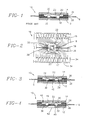
- FIG. 1 is a cross-sectional representation of a prior art housing 10 for encapsulating an electronic device 22.
- the typical method of manufacture is to fasten the leadframe 16 to the base component 12 using a first sealant 28.
- the first sealant is generally a low melting solder glass or a polymer adhesive.
- a typical solder glass for use in sealing electronic packages is a lead borate glass matrix usually containing one or more other glass components.
- One example of a solder glass is the mixture 75% - 85% PbO, 0.5% - 16% ZnO and 8% - 15% B2O3. Any solder glass with an appropriate coefficient of thermal expansion may be utilized.
- a typical polymer sealant is a heat curable epoxy such as novalac.
- a typical sealing profile for a solder glass is about 410° - 430°C for 10 minutes and for an epoxy a typical curing cycle is about 150° to 170°C for about 30 to 120 minutes.
- the electronic device 22 After the first sealant is cured and the leadframe affixed in place, the electronic device 22, often a silicon based semiconductor chip, is attached.
- the electronic device is attached either directly to the base component 12 by a die attach 32 or to a buffer (not shown) which is then fastened to the base component.
- a buffer system is disclosed in European Application No. 86 102 059.2 published September 17, 1986.
- the coefficient of thermal expansion of the base component or buffer determines the choice of die attach material 32 used. If the CTE of the base component or buffer is within about 10% the CTE of the electronic device, typically 49X10 ⁇ 7/°C, a hard solder such as 98% Au/2% Si may be used. If the CTE of the base component or buffer does not approach that of the electronic device, a more forgiving die attach is used. For example, a soft solder such as 95% Pb/5% Sn or an electrically conductive polymer adhesive such as a silver filled epoxy may be used.
- a thermal treatment is required to activate the die attach. If Au/Si solder is used this thermal treatment generally is about 420°C for about 5 seconds. For Pb/Sn solder, a temperature of about 200°C for about 20 seconds is used and for the filled polymer about 150°C for about 30 minutes. Regardless of the die attach chosen, the first sealant 28 is subjected to a second heating and cooling cycle.
- the lead wires 20 are next bonded to the electronic device 22 and inner lead portions 18 to electrically connect the electronic device to the outside world through leadframe 16.
- the lead wires are typically gold or aluminium wires or thin strips of copper foil if the process known as tape automated bonding (TAB) is used. Bonding may be by ultrasonic welding, thermal bonding or thermal compression bonding. Some heat of bonding may be transmitted through the leads subjecting the first sealant 28 to another thermal cycle. A typical bonding temperature is about 240°C for about 5 seconds.
- a second sealant 26 is applied to the cover componet 14.
- the second sealant is usually chosen to have the same composition as the first sealant 28 to insure chemical compatibility although this is not necessary as disclosed in previously cited U.S. Patent No. 4,704,626.
- the cover component 14 is then positioned adjacent to the leadframe 16 and bonded to the side of the leadframe opposite the base component. A sealing profile suitable to cure the second sealant 26 is required.
- the first sealant 28 is once more subjected to a thermal cycle.
- One embodiment of the present invention is to provide for the manufacture of a housing for an electronic device which does not subject the first sealant to the multiple thermal cycles of the prior art.
- FIGS. 2 and 3 illustrate the assembly of a housing 10 for an electronic device 22 in accordance with the present invention.
- the leadframe 16 is comprised of an electrically conductive material.
- Leadframes are typically fashioned from Alloy 42 (an iron-nickel alloy containing 58% Fe and 42% Ni), KOVAR (an iron-nickel-cobalt alloy containing 54% Fe, 29% Ni and 17% Co), copper or a copper based alloy.
- the leadframe may be plated or clad with a second material to enhance bonding to the sealant, improve corrosion resistance or improve appearance.
- the leadframe for a metal package is a copper based alloy such as C638 described in U.S. Patent Nos. 3,341,369 and 3,475,227 to Caule et al.
- dilute copper alloys essentially pure copper with trace amounts of additives, are also used as leadframes due to the high electrical conductivity they impart as compared to other copper alloys and added strength they have compared to pure copper.
- a typical dilute copper alloys for use in leadframes is C194 (2.35% Fe, 0.03% P, 0.12% Zn and the balance Cu).
- the leadframe is comprised of lead fingers 17 which are made up of inner lead portions 18 for bonding to the electronic device 22 and outer lead portions 19 for electrically connecting the electronic device to an external device, for example, by insertion into a printed circuit board.
- the leadframe also contains tie bars 34 to support the lead fingers 17 during assembly operations. The tie bars 34 are generally severed once the leadframe is in place to electrically isolate the leads from each other.
- Some leadframes also contain a centrally positioned die attach pad 36 which is connected to the tie bars by die attach pad supports 38.
- Leadframes with die attach pads are usually used in plastic encapsulated packages to provide a site to mount the chip and provide electrical contact to the back side of the chip. The use of a die attach pad in a plastic encapsulated package is disclosed in U.S. Patent No. 4,697,203 issued to Sakai el al. The use of a die attach pad with a metal package is discosed in U.S. Patent No. 4,656,499.
- the electronic device 22 which is typically a semiconductor chip made of silicon although other semiconductor materials such as germanium or gallium arsenide may also be used is attached to the die attach pad 36 by a die attach material 32.
- the die attach may be a eutectic solder such as gold based Au/Si or lead based such as 95% Pb/5% Sn, or a soft solder such as lead based 60% Pb/40% Sn or 92.5% Pb/5% Sn/2.5% Ag or a polymer adhesive such as a heat curable epoxy.
- die attach materials are given for the purpose of example and is not meant to be all encompassing, any suitable die attach material could be used within the scope of the present invention.
- an epoxy die attach it may be conducting or insulating dependent upon whether backside electrical contact is desired.
- the epoxy may be made electrically conductive by filling it with a conductive metal (for example, silver) powder.
- the electronic device 22 is next connected to the inner lead portions 18 through bonding wires 20.
- These wires are frequently made of thin, about 0. 025mm (0. 001 inch) diameter strands of gold or aluminum.
- thin strips of copper foil are used for TAB bonding as disclosed in U.S. Patent No. 4,330,790 issued to Burns.
- the wires 20 are bonded by conventional wire bonding techniques to bonding sites 39 on the electrically active face of the electronic device 22.
- the opposite ends of the wires are bonded to the inner portions 18 of the leadframe 16 thereby creating an electrical connection between the electronic device 22 and the outer lead portions 19.
- FIG. 3 shows an assembled package in accordance with the present invention.
- a base component 12 containing first sealant 28 and third sealant 40 is provided.
- the first sealant 28 is selected from the group consisting of nonconductive solder glasses, ceramics, thermosetting polymers and themoplastic polymers.
- the third sealant 40 is selected from the group consisting of solder glasses, ceramics, metal alloy solders, thermosetting polymers and thermoplastic polymers.
- the third sealant 40 is either a dielectric or an electrical conductor.
- the third sealant is usually made electrically conductive by filling it with a conductive metal powder. Carbon filling may be utilized.
- the third sealant 40 is also characterized by high thermal conductivity.
- Preferred third sealants 40 for the present invention are silver filled epoxy or soft solder such as Pb/Sn.
- the leadframe 16 is positioned adjacent to the sealant containing face of the base component. Frequently, the thickness of the first sealant 28 is greater than the thickness of the third sealant 40 and the difference is compensated for by downsetting the die attach pad support 38′. Downsetting also helps maintain electrical isolation between the inner lead portions and the die attach pad supports. In the alternative, after curing the first and third sealants, the die attach pad supports 38 may be severed.
- the leadframe is bonded to the base component by an appropriate curing cycle for the first and third sealants.
- An advantage of the present embodiment over an embodiment described hereinbelow is the package is open during the thermal cure so by-products of the cure, for example, chloride ions from an epoxy may escape into the atmosphere.
- a cover component 14 containing a nonconductive second sealant 26 selected from the same group as the first sealant 28 and frequently, although not necessarily identical to the first sealant is positioned adjacent to the unbonded side of the leadframe.
- the cover component is sealed to the leadframe by an appropriate thermal cycle thereby forming a housing for the electonic device.
- a second embodiment of the present invention seals the first 28 and second 26 sealants at the same time.
- a leadframe 16 with the electronic device 22 already die attached and wire bonded is disposed between a base component 12 and a cover componet 14.
- First sealant 28 is disposed between the first side of the leadframe and the base component.
- Third sealant 40 is disposed between the die attach pad and the base component.
- Second sealant 26 is disposed between the cover component and the second side of the leadframe.
- An appropriate thermal cycle is chosen to cure all three sealants simultaneously.
- the advantage of the second embodiment of the invention over the prior art is the first sealant 28 is subjected to only a cure cycle and not to excess thermal cycles.
- the structure of an electronic package made according to the present invention resembles the metal package sealed with solder glass disclosed in U.S. Patent No. 4,656,499 to Butt entitled Hermetically Sealed Semiconductor Casing.
- Butt method of assembly is completely different and does not encompass the improvements necessary to reduce thermal degradation of the sealants.
- FIG. 4 Another embodiment of the present invention is shown in FIG. 4.
- a housing for an electronic device 10 is assembled using either of the above disclosed embodiments.
- An aperture 42 is provided in the base component 12′.
- the aperture allows the escape of reaction by-products generated during the sealing cycle.
- the first sealant 28, second sealant 26 and third sealant 40 may all be cured at the same time and the accumulation of residue within the enclosure 30 of the housing is less than with previous embodiments.
- the third sealant 40 is a ring type seal surrounding the aperture 42. The seal 40 bonds the die attach pad to the base 12′.
- a second improvement realized by the aperture 42 within the base component 12′ is the proximity of the chip to outside influences.
- electricity passes through the device. Some of the electricity is converted into heat due to the internal resistance of the semiconductor circuitry. This heat reduces the operating life of the semiconductor chip and is preferably removed.
- Common means of removing the generated heat are metal heatsinks located below the chip and forced air or forced fluid cooling. An over view of these heatsink means may be found in the article entitled "Future Packages' Heat Transfer Will Affect PCB Designs" by Ernel R. Winkler which appeared in the April 1985 edition of ELECTRONIC PACKAGING & PRODUCTION.
- the aperture 42 permits a forced air or forced fluid cooling means to be positioned in close proximity to the electronic device 22.
- a cooling material with high heat capacity for example helium gas, results in improved cooling. This improved cooling becomes more important as the density of electronic circuits on the semiconductor device increases resulting in greater heat generation during operation of the chip.
- a solid material with high heat capacity for example copper or silver may be inserted into the aperture 42 and used as a conduit (heat sink) to transfer heat from the electronic device.
- a second aperture 44 within the cover component 14′.
- the aperture 44 is a vent for reaction by-products generated during the cure cycle.
- an inert thermally conductive gas such as helium or a thermally conductive, electrically non-conductive liquid or powder may optionally be injected into the package cavity 30 to provide additional thermal dissipation means for the electronic device 22.
- the aperture is then sealed by applying a suitable patch, for example a drop of solder 48 to the outer surface 46 of the cover component.
- the aperture 44 could be sealed by any preferred means such as plastic.
- the apertures 42 and 44 can be employed alone or in combination as desired.
Abstract
Description
- The present invention relates to a process for making a package to house an electronic device and the package so produced. The package is characterized by improved resistance to thermal degradation and improved dissipation of heat from the enclosed electronic device.
- Several basic package designs are used by the electronics industry to house integrated circuits. The integrated circuits, usually fashioned from a semiconductor material and typically from silicon, must be protected from the outside environment and must electrically connect to external components. Balanced against these requirements is a need to minimize cost of manufacture and assembly of the package.
- The electronics industry has generally followed one of two lines; maximimum protection of the electronic device for example with the ceramic dual-in-line package or minimum cost, for example by the encapsulated plastic package. There are distinct disadvantages to both concepts.
- The ceramic dual-in-line package (CERDIP) is comprised of two pieces of alumina or other ceramic glass bonded to a leadframe with a suitable solder glass forming a hermetic enclosure. A problem associated with a CERDIP is poor thermal dissipation. To maximize thermal dissipation capabilities of a CERDIP, beryllium oxide is sometimes substituted for aluminum oxide. While the thermal capabilities of the package is improved, the cost increases significantly. The CERDIP is generally used for high value electronic requirements, for example, state-of-the-art computers or military applications.
- Plastic packages usually comprise an electronic device mounted on a leadframe encapsulated with a plastic resin, generally an epoxy. The plastic package is less expensive to manufacture than the CERDIP and more adaptable to automated procedures. The plastic package is generally not hermetic and not suitable for high value electronic requirements. Additionally, the plastic package has poor thermal dissipation.
- Throughout this application, the term "hermetic" is used in accordance with Military Specification 883B and defined as a package cavity leak rate of less than 5 x 10⁻⁸ cm³/sec when measured using a helium tracer gas.
- A package which seeks to overcome the disadvantages of the CERDIP and the plastic package is the metal package. The metal package is comprised of a leadframe disposed between a metal or metal alloy cover and base component. The leadframe is bonded to the base and cover using an electrically insulating adhesive, typically a solder glass or polymer adhesive. Generally, a solder glass is used if a hermetic package is desired. Examples of a metal package using a solder glass may be found in U.S Patent Nos. 4,524,238, 4,532,222, 4,542,259, 4,607,276 and 4,656,499 all issued to Butt.
- A problem associated with the metal package is a mismatch in the coefficient of thermal expansion between the metal component and the conventinal CERDIP solder glasses. The metal components are typically copper or a copper based alloy and have coefficients of thermal expansion (CTE) of about 160 - 170X10⁻⁷/°C while the low temperature solder glasses were originally designed to match the CTE of aluminum oxide CERDIP packages and have a CTE of about 49X10⁻⁷/°C. If the CTE mismatch exceeds 10% the glass may fracture due to stresses introduced during thermal cycling resulting in a loss of hermeticity.
- Methods to get a close match in coefficients of thermal expansion include the use of a graded seal as disclosed in U.S. Patent No. 4,704,626 to Mahulikar et al and the use of appropriately chosen filler material such as calcium fluoride to change the coefficient of thermal expansion of the glass as disclosed in U.S. Patent Nos. 4,752,521 and 4,801,488.
- Hermetic metal packages have the added advantage of excellent dissipation of heat generated by the electronic device during operation. As metal packages contain a cavity, the surface of the electronic device is not subjected to stresses during thermal cycling as occurs with a molded plastic package.
- Metal packages have also been used to replace components in plastic packages. As with glass sealed packages, a metal leadframe is disposed between a metal or metal alloy base and cover component. The package is sealed with a polymer adhesive, typically an epoxy. Examples of a metal package with a polymer adhesive sealant are in U.S. Patent Nos. 4,461,924, 4,480,262 and 4,594,770 all to Butt and U.S. Patent No. 4,105,861 to Hascoe.
- Polymer adhesives are generally more compliant than sealing glasses. There is no need to match the coefficient of thermal expansion of the package components to the adhesive. Thermally induced stresses will be absorbed and damped by the polymer adhesive. A difficulty with the metal package utilizing a polymer adhesive is it is not hermetic in accordance with Mil. Spec. 883B.
- Additionally, the polymers are not thermally stable and tend to degrade during post-cure heating cycles. One method of evaluating the package sealant is commonly called the pressure cooker test. The test comprises immersion of a sealed package in a pressure cooker at 121°C, a relative humidity of 100% and a pressure of 2100 gm/cm² (30 psi) . It has been found that metal packages sealed with polymer adhesives delaminate within a relatively short amount of time during this test. This test is an accelerated environmental test and indicates how well the package will protect the electronic device from air and moisture.
- In accordance with the present invention, a leadframe containing a centrally positioned die attach pad is provided. An electronic device, typically a silicon semiconductor chip, is bonded to the die attach pad. The die attach pad is bonded to the package base and the base and cover components are sealed to the leadframe. The package goes through at least one fewer sealing cycle than prior art packages resulting in substantial improvements in the functional life of the sealant.
- In another embodiment of the present invention, an aperture is provided in the base component. The die attach pad is sealed over the aperture. The embodiment permits improved removal of heat from the electronic device.
- Accordingly, it is an object of the present invention to provide a metal package sealed with a polymer which is more resistant to thermal degradation.
- It is a further object of the present invention to provide a metal package with a polymer sealant requiring fewer assembly steps than present metal packages.
- It is yet another object of the present invention to provide a metal package with improved thermal dissipation characteristics.
- These and further objects and advantages will become more apparent from the following description and drawings in which like reference numerals depict like elements.
- FIG. 1 is a cross-sectional representation of a metal package as known from the prior art.
- FIG. 2 is a schematic representation of a leadframe with an electronic device affixed thereto in accordance with the present invention.
- FIG. 3 is a cross-sectional representation of a metal package in accordance with one embodiment of the present invention.
- FIG. 4 is a cross-sectional representation of a metal package in accordance with a second embodiment of the present invention.
- FIG. 1 is a cross-sectional representation of a
prior art housing 10 for encapsulating anelectronic device 22. The typical method of manufacture is to fasten theleadframe 16 to thebase component 12 using afirst sealant 28. The first sealant is generally a low melting solder glass or a polymer adhesive. A typical solder glass for use in sealing electronic packages is a lead borate glass matrix usually containing one or more other glass components. One example of a solder glass is the mixture 75% - 85% PbO, 0.5% - 16% ZnO and 8% - 15% B₂O₃. Any solder glass with an appropriate coefficient of thermal expansion may be utilized. A typical polymer sealant is a heat curable epoxy such as novalac. - A typical sealing profile for a solder glass is about 410° - 430°C for 10 minutes and for an epoxy a typical curing cycle is about 150° to 170°C for about 30 to 120 minutes.
- After the first sealant is cured and the leadframe affixed in place, the
electronic device 22, often a silicon based semiconductor chip, is attached. The electronic device is attached either directly to thebase component 12 by a die attach 32 or to a buffer (not shown) which is then fastened to the base component. A buffer system is disclosed in European Application No. 86 102 059.2 published September 17, 1986. - The coefficient of thermal expansion of the base component or buffer determines the choice of die attach
material 32 used. If the CTE of the base component or buffer is within about 10% the CTE of the electronic device, typically 49X10⁻⁷/°C, a hard solder such as 98% Au/2% Si may be used. If the CTE of the base component or buffer does not approach that of the electronic device, a more forgiving die attach is used. For example, a soft solder such as 95% Pb/5% Sn or an electrically conductive polymer adhesive such as a silver filled epoxy may be used. - A thermal treatment is required to activate the die attach. If Au/Si solder is used this thermal treatment generally is about 420°C for about 5 seconds. For Pb/Sn solder, a temperature of about 200°C for about 20 seconds is used and for the filled polymer about 150°C for about 30 minutes. Regardless of the die attach chosen, the
first sealant 28 is subjected to a second heating and cooling cycle. - The
lead wires 20 are next bonded to theelectronic device 22 andinner lead portions 18 to electrically connect the electronic device to the outside world throughleadframe 16. The lead wires are typically gold or aluminium wires or thin strips of copper foil if the process known as tape automated bonding (TAB) is used. Bonding may be by ultrasonic welding, thermal bonding or thermal compression bonding. Some heat of bonding may be transmitted through the leads subjecting thefirst sealant 28 to another thermal cycle. A typical bonding temperature is about 240°C for about 5 seconds. - Next, a
second sealant 26 is applied to thecover componet 14. The second sealant is usually chosen to have the same composition as thefirst sealant 28 to insure chemical compatibility although this is not necessary as disclosed in previously cited U.S. Patent No. 4,704,626. Thecover component 14 is then positioned adjacent to theleadframe 16 and bonded to the side of the leadframe opposite the base component. A sealing profile suitable to cure thesecond sealant 26 is required. Thefirst sealant 28 is once more subjected to a thermal cycle. - The prior art package is now complete. If first and
second sealants first sealant 28 impacts detrimentally on the integrity of the package. One embodiment of the present invention is to provide for the manufacture of a housing for an electronic device which does not subject the first sealant to the multiple thermal cycles of the prior art. - FIGS. 2 and 3 illustrate the assembly of a
housing 10 for anelectronic device 22 in accordance with the present invention. - Referring to FIG. 2, a schematic of a
leadframe 16 as known in the art is shown. Theleadframe 16 is comprised of an electrically conductive material. Leadframes are typically fashioned from Alloy 42 (an iron-nickel alloy containing 58% Fe and 42% Ni), KOVAR (an iron-nickel-cobalt alloy containing 54% Fe, 29% Ni and 17% Co), copper or a copper based alloy. The leadframe may be plated or clad with a second material to enhance bonding to the sealant, improve corrosion resistance or improve appearance. Typically the leadframe for a metal package is a copper based alloy such as C638 described in U.S. Patent Nos. 3,341,369 and 3,475,227 to Caule et al. or C724 as described in U.S. Patent No. 4,594,221 to Caron et al. Alloys C638, C724, C7025 and similar copper based alloys form a refractory oxide layer which facilitates bonding of the alloy to a solder glass. Alternatively, dilute copper alloys, essentially pure copper with trace amounts of additives, are also used as leadframes due to the high electrical conductivity they impart as compared to other copper alloys and added strength they have compared to pure copper. A typical dilute copper alloys for use in leadframes is C194 (2.35% Fe, 0.03% P, 0.12% Zn and the balance Cu). - The leadframe is comprised of
lead fingers 17 which are made up ofinner lead portions 18 for bonding to theelectronic device 22 andouter lead portions 19 for electrically connecting the electronic device to an external device, for example, by insertion into a printed circuit board. The leadframe also contains tie bars 34 to support thelead fingers 17 during assembly operations. The tie bars 34 are generally severed once the leadframe is in place to electrically isolate the leads from each other. Some leadframes also contain a centrally positioned die attachpad 36 which is connected to the tie bars by die attach pad supports 38. Leadframes with die attach pads are usually used in plastic encapsulated packages to provide a site to mount the chip and provide electrical contact to the back side of the chip. The use of a die attach pad in a plastic encapsulated package is disclosed in U.S. Patent No. 4,697,203 issued to Sakai el al. The use of a die attach pad with a metal package is discosed in U.S. Patent No. 4,656,499. - In accordance with the present invention, the
electronic device 22 which is typically a semiconductor chip made of silicon although other semiconductor materials such as germanium or gallium arsenide may also be used is attached to the die attachpad 36 by a die attachmaterial 32. Dependent upon the composition of theleadframe 16 and the corresponding coefficient of thermal expansion of the leadframe, the die attach may be a eutectic solder such as gold based Au/Si or lead based such as 95% Pb/5% Sn, or a soft solder such as lead based 60% Pb/40% Sn or 92.5% Pb/5% Sn/2.5% Ag or a polymer adhesive such as a heat curable epoxy. The list of die attach materials is given for the purpose of example and is not meant to be all encompassing, any suitable die attach material could be used within the scope of the present invention. If an epoxy die attach is used, it may be conducting or insulating dependent upon whether backside electrical contact is desired. The epoxy may be made electrically conductive by filling it with a conductive metal (for example, silver) powder. - The
electronic device 22 is next connected to theinner lead portions 18 throughbonding wires 20. These wires are frequently made of thin, about 0. 025mm (0. 001 inch) diameter strands of gold or aluminum. In the alternative, thin strips of copper foil are used for TAB bonding as disclosed in U.S. Patent No. 4,330,790 issued to Burns. Thewires 20 are bonded by conventional wire bonding techniques tobonding sites 39 on the electrically active face of theelectronic device 22. The opposite ends of the wires are bonded to theinner portions 18 of theleadframe 16 thereby creating an electrical connection between theelectronic device 22 and theouter lead portions 19. - The
leadframe 16 containing the die attached and wire bondedelectronic device 22 is now ready for further assembly in accordance with the present invention. Reference is made to FIG. 3 which shows an assembled package in accordance with the present invention. - In a first process embodiment, a
base component 12 containingfirst sealant 28 andthird sealant 40 is provided. Thefirst sealant 28 is selected from the group consisting of nonconductive solder glasses, ceramics, thermosetting polymers and themoplastic polymers. Thethird sealant 40 is selected from the group consisting of solder glasses, ceramics, metal alloy solders, thermosetting polymers and thermoplastic polymers. Dependent on whether the back side of the chip is to be electrically connected to the package base or electrically isolated, thethird sealant 40 is either a dielectric or an electrical conductor. The third sealant is usually made electrically conductive by filling it with a conductive metal powder. Carbon filling may be utilized. Thethird sealant 40 is also characterized by high thermal conductivity. Preferredthird sealants 40 for the present invention are silver filled epoxy or soft solder such as Pb/Sn. Theleadframe 16 is positioned adjacent to the sealant containing face of the base component. Frequently, the thickness of thefirst sealant 28 is greater than the thickness of thethird sealant 40 and the difference is compensated for by downsetting the die attachpad support 38′. Downsetting also helps maintain electrical isolation between the inner lead portions and the die attach pad supports. In the alternative, after curing the first and third sealants, the die attach pad supports 38 may be severed. - The leadframe is bonded to the base component by an appropriate curing cycle for the first and third sealants. An advantage of the present embodiment over an embodiment described hereinbelow is the package is open during the thermal cure so by-products of the cure, for example, chloride ions from an epoxy may escape into the atmosphere.
- A
cover component 14 containing a nonconductivesecond sealant 26 selected from the same group as thefirst sealant 28 and frequently, although not necessarily identical to the first sealant is positioned adjacent to the unbonded side of the leadframe. The cover component is sealed to the leadframe by an appropriate thermal cycle thereby forming a housing for the electonic device. - An improvement of the present invention over the prior art is the first sealant is subjected to only one additional thermal cycle, thereby reducing the thermal degradation.
- A second embodiment of the present invention seals the first 28 and second 26 sealants at the same time. A
leadframe 16 with theelectronic device 22 already die attached and wire bonded is disposed between abase component 12 and acover componet 14.First sealant 28 is disposed between the first side of the leadframe and the base component.Third sealant 40 is disposed between the die attach pad and the base component.Second sealant 26 is disposed between the cover component and the second side of the leadframe. An appropriate thermal cycle is chosen to cure all three sealants simultaneously. - The advantage of the second embodiment of the invention over the prior art is the
first sealant 28 is subjected to only a cure cycle and not to excess thermal cycles. The structure of an electronic package made according to the present invention resembles the metal package sealed with solder glass disclosed in U.S. Patent No. 4,656,499 to Butt entitled Hermetically Sealed Semiconductor Casing. However the Butt method of assembly is completely different and does not encompass the improvements necessary to reduce thermal degradation of the sealants. - Another embodiment of the present invention is shown in FIG. 4. A housing for an
electronic device 10 is assembled using either of the above disclosed embodiments. Anaperture 42 is provided in thebase component 12′. The aperture allows the escape of reaction by-products generated during the sealing cycle. Thefirst sealant 28,second sealant 26 andthird sealant 40 may all be cured at the same time and the accumulation of residue within theenclosure 30 of the housing is less than with previous embodiments. Thethird sealant 40 is a ring type seal surrounding theaperture 42. Theseal 40 bonds the die attach pad to the base 12′. - A second improvement realized by the
aperture 42 within thebase component 12′ is the proximity of the chip to outside influences. As theelectronic device 22 is operated, electricity passes through the device. Some of the electricity is converted into heat due to the internal resistance of the semiconductor circuitry. This heat reduces the operating life of the semiconductor chip and is preferably removed. Common means of removing the generated heat are metal heatsinks located below the chip and forced air or forced fluid cooling. An over view of these heatsink means may be found in the article entitled "Future Packages' Heat Transfer Will Affect PCB Designs" by Ernel R. Winkler which appeared in the April 1985 edition of ELECTRONIC PACKAGING & PRODUCTION. - The
aperture 42 permits a forced air or forced fluid cooling means to be positioned in close proximity to theelectronic device 22. The use of a cooling material with high heat capacity, for example helium gas, results in improved cooling. This improved cooling becomes more important as the density of electronic circuits on the semiconductor device increases resulting in greater heat generation during operation of the chip. - Rather than a fluid, a solid material with high heat capacity, for example copper or silver may be inserted into the
aperture 42 and used as a conduit (heat sink) to transfer heat from the electronic device. - Yet another embodiment of the present invention is the inclusion of a
second aperture 44 within thecover component 14′. Theaperture 44 is a vent for reaction by-products generated during the cure cycle. After the cure cycle is completed, an inert thermally conductive gas such as helium or a thermally conductive, electrically non-conductive liquid or powder may optionally be injected into thepackage cavity 30 to provide additional thermal dissipation means for theelectronic device 22. The aperture is then sealed by applying a suitable patch, for example a drop of solder 48 to theouter surface 46 of the cover component. Alternatively, theaperture 44 could be sealed by any preferred means such as plastic. Theapertures - While the present invention has been described in terms of a metal package, the techniques described are suitable for ceramic packages, such as CERDIP, or plastic packages.
- It is apparent there has been provided in accordance with this invention means of assembling electronic packages and the products of those assembly means which fully satisfy the objects, means and advantages set forth hereinbelow. While the invention has been described in combination with specific embodiments thereof, it is evident that many alternatives, modifications and variations will be apparent to those skilled in the art in light of the forgoing description. Accordingly, it is intended to embrace all such alternatives, modifications and variations as fall within the spirit and broad scope of the appended claims.
Claims (37)
providing an electrically conductive leadframe 16, said leadframe 16 having first and second surfaces and comprised of a plurality of lead fingers 18 disposed about a centrally positioned die attach pad 36, said electronic device 22 bonded to said die attach pad 36 and electrically connected to said leads 18;
providing a first 28, second 26 and third 40 bonding means;
providing a base component 12;
providing a cover component 14;
bonding said base component 12 to said first surface of said leadframe 16 with said first bonding means 28 and at essentially the same time bonding said base component 12 to said die attach pad 36 with said third bonding means 40; and
bonding said cover component 14 to said second surface of said leadframe 16 with said second bonding means 26.
a base component 12 prime containing a first aperture 42;
a cover component 14;
a leadframe 16 with first and second opposing sides disposed between said base component 12′ and said cover component 14, said leadframe 16 containing a plurality of leads 17 disposed about a centrally positioned die attach pad 36, said die attach pad 36 positioned to seal said first aperture 42 and adapted to support said electronic device 22, said electronic device 22 electrically connected to said leads 17;
a first bonding means 28 to seal said base component 12′ to said first side of said leadframe 16;
a second bonding means 26 to seal said cover component 14 to said second side of said leadframe 16; and
a third bonding means 40 to seal die attach pad 36 to said base component 12′.
a base component 12;
a cover component 14 prime containing a second aperture 44 sealed with a plug 48;
a leadframe 16 with first and second opposing sides disposed between said base component 12 and said cover component 14 prime , said leadframe 16 containing a plurality of leads 17 disposed about a centrally positioned die attach pad 36 and adapted to support said electronic device 22, said electronic device 22 electrically connected to said leads 17;
a first bonding means 28 to seal said base component 12 to said first side of said leadframe 16;
a second bonding means 26 to seal said cover component 12 to said second side of said leadframe 16; and
a third bonding means 40 to seal said cover component 14′ to said base component 12.
a base component 12 containing first aperture 42;
a cover component 14 prime containing a second aperture 44, said second aperture 44 sealed with a plug 48;
a leadframe 16 with first and second opposing sides disposed between said base component 12′ and said cover component 14 prime , said leadframe 16 containing a plurality of leads 17 disposed about a centrally positioned die attach pad 36, said die attach pad 36 positioned to seal said first aperture 42 and adapted to support said electronic device 22, said electronic device 22 electrically connected to said leads 17;
a first bonding means 28 to seal said base component 12 prime to said first side of said leadframe 16;
a second bonding means 26 to seal said cover component 14′ to said second side of said leadframe 16; and
a third bonding means 40 positioned about the edge of said first aperture 42 and disposed between said base component 12′ and said die attach component 36.
Priority Applications (1)
| Application Number | Priority Date | Filing Date | Title |
|---|---|---|---|
| DE1989627771 DE68927771T2 (en) | 1989-10-03 | 1989-10-03 | Process for manufacturing an electronics package |
Applications Claiming Priority (1)
| Application Number | Priority Date | Filing Date | Title |
|---|---|---|---|
| US07/154,544 US4897508A (en) | 1988-02-10 | 1988-02-10 | Metal electronic package |
Publications (3)
| Publication Number | Publication Date |
|---|---|
| EP0421005A2 true EP0421005A2 (en) | 1991-04-10 |
| EP0421005A3 EP0421005A3 (en) | 1991-05-02 |
| EP0421005B1 EP0421005B1 (en) | 1997-02-12 |
Family
ID=22551746
Family Applications (1)
| Application Number | Title | Priority Date | Filing Date |
|---|---|---|---|
| EP89118353A Expired - Lifetime EP0421005B1 (en) | 1988-02-10 | 1989-10-03 | Process of assembling an electronic package |
Country Status (2)
| Country | Link |
|---|---|
| US (1) | US4897508A (en) |
| EP (1) | EP0421005B1 (en) |
Cited By (5)
| Publication number | Priority date | Publication date | Assignee | Title |
|---|---|---|---|---|
| WO1992020096A1 (en) * | 1991-05-06 | 1992-11-12 | Sensonor A.S | Arrangement for encasing a functional device, and a process for the production of same |
| EP0664924A1 (en) * | 1992-10-13 | 1995-08-02 | Olin Corporation | Metal electronic package with reduced seal width |
| FR2721437A1 (en) * | 1994-06-17 | 1995-12-22 | Xeram N | Hermetic casing with improved heat dissipation for encapsulating electronic components |
| EP0754350A1 (en) * | 1994-04-05 | 1997-01-22 | Olin Corporation | Cavity filled metal electronic package |
| CN102645820A (en) * | 2011-02-22 | 2012-08-22 | 鸿富锦精密工业(深圳)有限公司 | Camera module |
Families Citing this family (67)
| Publication number | Priority date | Publication date | Assignee | Title |
|---|---|---|---|---|
| US4897508A (en) * | 1988-02-10 | 1990-01-30 | Olin Corporation | Metal electronic package |
| US5502889A (en) * | 1988-06-10 | 1996-04-02 | Sheldahl, Inc. | Method for electrically and mechanically connecting at least two conductive layers |
| US5155299A (en) * | 1988-10-05 | 1992-10-13 | Olin Corporation | Aluminum alloy semiconductor packages |
| US5073521A (en) * | 1989-11-15 | 1991-12-17 | Olin Corporation | Method for housing a tape-bonded electronic device and the package employed |
| US5081327A (en) * | 1990-03-28 | 1992-01-14 | Cabot Corporation | Sealing system for hermetic microchip packages |
| US5043534A (en) * | 1990-07-02 | 1991-08-27 | Olin Corporation | Metal electronic package having improved resistance to electromagnetic interference |
| US5261157A (en) * | 1991-01-22 | 1993-11-16 | Olin Corporation | Assembly of electronic packages by vacuum lamination |
| US5132773A (en) * | 1991-02-06 | 1992-07-21 | Olin Corporation | Carrier ring having first and second ring means with bonded surfaces |
| KR940001148B1 (en) * | 1991-04-16 | 1994-02-14 | 삼성전자 주식회사 | Semiconductor package |
| US5144709A (en) * | 1991-05-03 | 1992-09-08 | Olin Corporation | Formation of shapes in a metal workpiece |
| US5272800A (en) * | 1991-07-01 | 1993-12-28 | Olin Corporation | Method and apparatus for forming and positioning a preform on a workpiece |
| US5247133A (en) * | 1991-08-29 | 1993-09-21 | Motorola, Inc. | High-vacuum substrate enclosure |
| JP3088193B2 (en) * | 1992-06-05 | 2000-09-18 | 三菱電機株式会社 | Method for manufacturing semiconductor device having LOC structure and lead frame used therein |
| US5239131A (en) * | 1992-07-13 | 1993-08-24 | Olin Corporation | Electronic package having controlled epoxy flow |
| US5389739A (en) * | 1992-12-15 | 1995-02-14 | Hewlett-Packard Company | Electronic device packaging assembly |
| JPH06196603A (en) * | 1992-12-23 | 1994-07-15 | Shinko Electric Ind Co Ltd | Manufacture of lead frame |
| US5727310A (en) * | 1993-01-08 | 1998-03-17 | Sheldahl, Inc. | Method of manufacturing a multilayer electronic circuit |
| JPH06209058A (en) * | 1993-01-12 | 1994-07-26 | Mitsubishi Electric Corp | Semiconductor device, its manufacture, and its mounting method |
| US5477008A (en) * | 1993-03-19 | 1995-12-19 | Olin Corporation | Polymer plug for electronic packages |
| US5413965A (en) * | 1993-09-13 | 1995-05-09 | Motorola, Inc. | Method of making microelectronic device package containing a liquid |
| US5578869A (en) * | 1994-03-29 | 1996-11-26 | Olin Corporation | Components for housing an integrated circuit device |
| AU2231795A (en) * | 1994-04-14 | 1995-11-10 | Olin Corporation | Electronic package having improved wire bonding capability |
| US5436407A (en) * | 1994-06-13 | 1995-07-25 | Integrated Packaging Assembly Corporation | Metal semiconductor package with an external plastic seal |
| US5455387A (en) * | 1994-07-18 | 1995-10-03 | Olin Corporation | Semiconductor package with chip redistribution interposer |
| TW309654B (en) * | 1995-03-29 | 1997-07-01 | Olin Corp | |
| US6388203B1 (en) | 1995-04-04 | 2002-05-14 | Unitive International Limited | Controlled-shaped solder reservoirs for increasing the volume of solder bumps, and structures formed thereby |
| DE69628161T2 (en) | 1995-04-05 | 2004-03-25 | Unitive International Ltd. | A SOLDERING STRUCTURE FOR A MICROELECTRONIC SUBSTRATE |
| SG59997A1 (en) * | 1995-06-07 | 1999-02-22 | Ibm | Apparatus and process for improved die adhesion to organic chip carries |
| KR0159987B1 (en) * | 1995-07-05 | 1998-12-01 | 아남산업주식회사 | Heat sink structure of ball grid array package |
| US6084299A (en) * | 1995-11-09 | 2000-07-04 | International Business Machines Corporation | Integrated circuit package including a heat sink and an adhesive |
| US5894167A (en) * | 1996-05-08 | 1999-04-13 | Micron Technology, Inc. | Encapsulant dam standoff for shell-enclosed die assemblies |
| US6025767A (en) * | 1996-08-05 | 2000-02-15 | Mcnc | Encapsulated micro-relay modules and methods of fabricating same |
| US5868887A (en) * | 1996-11-08 | 1999-02-09 | W. L. Gore & Associates, Inc. | Method for minimizing warp and die stress in the production of an electronic assembly |
| US5837556A (en) * | 1997-01-06 | 1998-11-17 | Sundstrand Corporation | Method of removing a component from a substrate |
| TW449844B (en) * | 1997-05-17 | 2001-08-11 | Hyundai Electronics Ind | Ball grid array package having an integrated circuit chip |
| GB2373924B (en) * | 1997-05-17 | 2002-11-13 | Hyundai Electronics Ind | Ball grid array package |
| US6045711A (en) * | 1997-12-29 | 2000-04-04 | Industrial Technology Research Institute | Vacuum seal for field emission arrays |
| US6036872A (en) | 1998-03-31 | 2000-03-14 | Honeywell Inc. | Method for making a wafer-pair having sealed chambers |
| US6359333B1 (en) * | 1998-03-31 | 2002-03-19 | Honeywell International Inc. | Wafer-pair having deposited layer sealed chambers |
| DE10065965B4 (en) * | 2000-03-11 | 2007-11-29 | Geyer Ag | Production method for a current sensor of the microsystem technology |
| US6989588B2 (en) * | 2000-04-13 | 2006-01-24 | Fairchild Semiconductor Corporation | Semiconductor device including molded wireless exposed drain packaging |
| KR100375720B1 (en) * | 2000-10-09 | 2003-03-15 | 삼성전자주식회사 | Semiconductor package and method for manufacturing thereof |
| WO2002039802A2 (en) * | 2000-11-10 | 2002-05-16 | Unitive Electronics, Inc. | Methods of positioning components using liquid prime movers and related structures |
| US6863209B2 (en) | 2000-12-15 | 2005-03-08 | Unitivie International Limited | Low temperature methods of bonding components |
| US7566587B2 (en) * | 2001-12-03 | 2009-07-28 | Azimuth Industrial Co., Inc. | Method and apparatus for packaging electronic components |
| US7547623B2 (en) * | 2002-06-25 | 2009-06-16 | Unitive International Limited | Methods of forming lead free solder bumps |
| US7531898B2 (en) * | 2002-06-25 | 2009-05-12 | Unitive International Limited | Non-Circular via holes for bumping pads and related structures |
| AU2003256360A1 (en) * | 2002-06-25 | 2004-01-06 | Unitive International Limited | Methods of forming electronic structures including conductive shunt layers and related structures |
| TWI225899B (en) * | 2003-02-18 | 2005-01-01 | Unitive Semiconductor Taiwan C | Etching solution and method for manufacturing conductive bump using the etching solution to selectively remove barrier layer |
| JP4223851B2 (en) * | 2003-03-31 | 2009-02-12 | ミツミ電機株式会社 | Small camera module |
| US6900525B2 (en) * | 2003-05-21 | 2005-05-31 | Kyocera America, Inc. | Semiconductor package having filler metal of gold/silver/copper alloy |
| JP2005039152A (en) * | 2003-07-18 | 2005-02-10 | Shinko Electric Ind Co Ltd | Method of manufacturing semiconductor device |
| US7049216B2 (en) * | 2003-10-14 | 2006-05-23 | Unitive International Limited | Methods of providing solder structures for out plane connections |
| WO2005101499A2 (en) | 2004-04-13 | 2005-10-27 | Unitive International Limited | Methods of forming solder bumps on exposed metal pads and related structures |
| US20060205170A1 (en) * | 2005-03-09 | 2006-09-14 | Rinne Glenn A | Methods of forming self-healing metal-insulator-metal (MIM) structures and related devices |
| US7674701B2 (en) | 2006-02-08 | 2010-03-09 | Amkor Technology, Inc. | Methods of forming metal layers using multi-layer lift-off patterns |
| US7932615B2 (en) * | 2006-02-08 | 2011-04-26 | Amkor Technology, Inc. | Electronic devices including solder bumps on compliant dielectric layers |
| JP2007287967A (en) * | 2006-04-18 | 2007-11-01 | Shinko Electric Ind Co Ltd | Electronic-component apparatus |
| US7700414B1 (en) | 2007-02-22 | 2010-04-20 | Unisem (Mauritius) Holdings Limited | Method of making flip-chip package with underfill |
| DE102007019096B4 (en) * | 2007-04-23 | 2015-03-12 | Continental Automotive Gmbh | electronics housing |
| KR101126767B1 (en) * | 2007-10-26 | 2012-03-29 | 삼성테크윈 주식회사 | Method for Manufacturing Printed Circuit Board And Printed Circuit Board Manufactured by the Method |
| US8105880B2 (en) * | 2007-12-05 | 2012-01-31 | Analog Devices, Inc. | Method for attaching a semiconductor die to a leadframe, and a semiconductor device |
| US8110445B2 (en) * | 2009-05-06 | 2012-02-07 | Infineon Technologies Ag | High power ceramic on copper package |
| TWI483056B (en) * | 2011-02-21 | 2015-05-01 | Hon Hai Prec Ind Co Ltd | Camera module |
| KR101237668B1 (en) * | 2011-08-10 | 2013-02-26 | 삼성전기주식회사 | Semiconductor package substrate |
| US9873468B2 (en) * | 2014-08-01 | 2018-01-23 | Howe And Howe Technologies, Inc. | Versatile off-road chair |
| US10014189B2 (en) * | 2015-06-02 | 2018-07-03 | Ngk Spark Plug Co., Ltd. | Ceramic package with brazing material near seal member |
Citations (4)
| Publication number | Priority date | Publication date | Assignee | Title |
|---|---|---|---|---|
| US4594770A (en) * | 1982-07-15 | 1986-06-17 | Olin Corporation | Method of making semiconductor casing |
| WO1988007761A1 (en) * | 1987-03-27 | 1988-10-06 | Olin Corporation | Metal packages having improved thermal dissipation |
| US4780572A (en) * | 1985-03-04 | 1988-10-25 | Ngk Spark Plug Co., Ltd. | Device for mounting semiconductors |
| US4897508A (en) * | 1988-02-10 | 1990-01-30 | Olin Corporation | Metal electronic package |
Family Cites Families (21)
| Publication number | Priority date | Publication date | Assignee | Title |
|---|---|---|---|---|
| US3341369A (en) * | 1965-03-03 | 1967-09-12 | Olin Mathieson | Copper base alloys and process for preparing same |
| US3475227A (en) * | 1966-10-04 | 1969-10-28 | Olin Mathieson | Copper base alloys and process for preparing same |
| US3728177A (en) * | 1970-07-30 | 1973-04-17 | Olin Corp | Method of producing a flexible laminate copper circuit |
| US3871018A (en) * | 1971-03-26 | 1975-03-11 | Ferranti Ltd | Construction of packages for semiconductor devices |
| US3943623A (en) * | 1974-08-23 | 1976-03-16 | Nitto Electric Industrial Co., Ltd. | Hollow cavity package electronic unit |
| US4105861A (en) * | 1975-09-29 | 1978-08-08 | Semi-Alloys, Inc. | Hermetically sealed container for semiconductor and other electronic devices |
| US4330790A (en) * | 1980-03-24 | 1982-05-18 | National Semiconductor Corporation | Tape operated semiconductor device packaging |
| US4410927A (en) * | 1982-01-21 | 1983-10-18 | Olin Corporation | Casing for an electrical component having improved strength and heat transfer characteristics |
| US4461924A (en) * | 1982-01-21 | 1984-07-24 | Olin Corporation | Semiconductor casing |
| US4480262A (en) * | 1982-07-15 | 1984-10-30 | Olin Corporation | Semiconductor casing |
| US4656499A (en) * | 1982-08-05 | 1987-04-07 | Olin Corporation | Hermetically sealed semiconductor casing |
| US4525422A (en) * | 1982-11-22 | 1985-06-25 | Olin Corporation | Adhesion primers for encapsulating epoxies |
| US4582556A (en) * | 1982-11-22 | 1986-04-15 | Olin Corporation | Adhesion primers for encapsulating epoxies |
| US4521469A (en) * | 1982-11-22 | 1985-06-04 | Olin Corporation | Casing for electronic components |
| US4524238A (en) * | 1982-12-29 | 1985-06-18 | Olin Corporation | Semiconductor packages |
| US4532222A (en) * | 1983-03-21 | 1985-07-30 | Olin Corporation | Reinforced glass composites |
| US4607276A (en) * | 1984-03-08 | 1986-08-19 | Olin Corporation | Tape packages |
| JPS60257546A (en) * | 1984-06-04 | 1985-12-19 | Mitsubishi Electric Corp | Semiconductor device and manufacture thereof |
| US4542259A (en) * | 1984-09-19 | 1985-09-17 | Olin Corporation | High density packages |
| US4594221A (en) * | 1985-04-26 | 1986-06-10 | Olin Corporation | Multipurpose copper alloys with moderate conductivity and high strength |
| US4704626A (en) * | 1985-07-08 | 1987-11-03 | Olin Corporation | Graded sealing systems for semiconductor package |
-
1988
- 1988-02-10 US US07/154,544 patent/US4897508A/en not_active Expired - Lifetime
-
1989
- 1989-10-03 EP EP89118353A patent/EP0421005B1/en not_active Expired - Lifetime
Patent Citations (4)
| Publication number | Priority date | Publication date | Assignee | Title |
|---|---|---|---|---|
| US4594770A (en) * | 1982-07-15 | 1986-06-17 | Olin Corporation | Method of making semiconductor casing |
| US4780572A (en) * | 1985-03-04 | 1988-10-25 | Ngk Spark Plug Co., Ltd. | Device for mounting semiconductors |
| WO1988007761A1 (en) * | 1987-03-27 | 1988-10-06 | Olin Corporation | Metal packages having improved thermal dissipation |
| US4897508A (en) * | 1988-02-10 | 1990-01-30 | Olin Corporation | Metal electronic package |
Non-Patent Citations (5)
| Title |
|---|
| PATENT ABSTRACTS OF JAPAN, Vol. 10, No. 343 (E-456), 19 November 1986; & JP,A,61 145 849 (NGK SPARK PLUG CO. LTD.) 03-07-1986, whole document. * |
| PATENT ABSTRACTS OF JAPAN, vol. 12, no. 379 (E-667), 11th October 1988; & JP-A-63 127 540 * |
| PATENT ABSTRACTS OF JAPAN, Vol. 2, No. 102 (E-052), 23 August 1978; & JP,A,53 068 573 (MITSUBISHI ELECTRIC CORP.), 19-06-1978, whole document. * |
| PATENT ABSTRACTS OF JAPAN, vol. 2, no. 102 (E-052), 23rd August 1978; & JP-A-53 68 573 * |
| PATENT ABSTRACTS OF JAPAN, vol. 9, no. 118 (E-316), 23rd May 1985; & JP-A-60 007 739 * |
Cited By (9)
| Publication number | Priority date | Publication date | Assignee | Title |
|---|---|---|---|---|
| WO1992020096A1 (en) * | 1991-05-06 | 1992-11-12 | Sensonor A.S | Arrangement for encasing a functional device, and a process for the production of same |
| AU649139B2 (en) * | 1991-05-06 | 1994-05-12 | Sensonor A.S | Arrangement for encasing a functional device, and a process for the production of same |
| EP0664924A1 (en) * | 1992-10-13 | 1995-08-02 | Olin Corporation | Metal electronic package with reduced seal width |
| EP0664924A4 (en) * | 1992-10-13 | 1995-08-30 | Olin Corporation | Metal electronic package with reduced seal width. |
| EP0754350A1 (en) * | 1994-04-05 | 1997-01-22 | Olin Corporation | Cavity filled metal electronic package |
| EP0754350A4 (en) * | 1994-04-05 | 1998-10-07 | Olin Corp | Cavity filled metal electronic package |
| FR2721437A1 (en) * | 1994-06-17 | 1995-12-22 | Xeram N | Hermetic casing with improved heat dissipation for encapsulating electronic components |
| CN102645820A (en) * | 2011-02-22 | 2012-08-22 | 鸿富锦精密工业(深圳)有限公司 | Camera module |
| CN102645820B (en) * | 2011-02-22 | 2016-08-03 | 广州美电恩智电子科技有限公司 | Camera module |
Also Published As
| Publication number | Publication date |
|---|---|
| EP0421005B1 (en) | 1997-02-12 |
| EP0421005A3 (en) | 1991-05-02 |
| US4897508A (en) | 1990-01-30 |
Similar Documents
| Publication | Publication Date | Title |
|---|---|---|
| US4897508A (en) | Metal electronic package | |
| CA1200923A (en) | Semiconductor packages | |
| US5458716A (en) | Methods for manufacturing a thermally enhanced molded cavity package having a parallel lid | |
| US5389739A (en) | Electronic device packaging assembly | |
| US4961106A (en) | Metal packages having improved thermal dissipation | |
| US4594770A (en) | Method of making semiconductor casing | |
| US4480262A (en) | Semiconductor casing | |
| US4577056A (en) | Hermetically sealed metal package | |
| US5043534A (en) | Metal electronic package having improved resistance to electromagnetic interference | |
| US5602059A (en) | Semiconductor device and method for manufacturing same | |
| US5650663A (en) | Electronic package with improved thermal properties | |
| US5144412A (en) | Process for manufacturing plastic pin grid arrays and the product produced thereby | |
| US4965227A (en) | Process for manufacturing plastic pin grid arrays and the product produced thereby | |
| JP4362366B2 (en) | Method for forming air cavity package of semiconductor circuit element | |
| EP0084866A2 (en) | Semiconductor casing | |
| US20030011054A1 (en) | Power module package having improved heat dissipating capability | |
| US6759752B2 (en) | Single unit automated assembly of flex enhanced ball grid array packages | |
| US3714370A (en) | Plastic package assembly for electronic circuit and process for producing the package | |
| AU2002310466A1 (en) | Use of diverse materials in air-cavity packaging of electronic devices | |
| JPH02342A (en) | Attachment of integrated circuit chip and package assembly | |
| KR20020095053A (en) | Power module package improved heat radiating capability and method for manufacturing the same | |
| JPS5893358A (en) | Semiconductor device | |
| CN87104825A (en) | The large scale integrated circuit encapsulation that heat dispersion has improved | |
| KR0168841B1 (en) | Metal electronic package and the manufacture method | |
| CA1304172C (en) | Metal electronic package |
Legal Events
| Date | Code | Title | Description |
|---|---|---|---|
| PUAI | Public reference made under article 153(3) epc to a published international application that has entered the european phase |
Free format text: ORIGINAL CODE: 0009012 |
|
| PUAL | Search report despatched |
Free format text: ORIGINAL CODE: 0009013 |
|
| AK | Designated contracting states |
Kind code of ref document: A2 Designated state(s): DE FR GB IT NL |
|
| AK | Designated contracting states |
Kind code of ref document: A3 Designated state(s): DE FR GB IT NL |
|
| 17P | Request for examination filed |
Effective date: 19911104 |
|
| 17Q | First examination report despatched |
Effective date: 19930402 |
|
| GRAH | Despatch of communication of intention to grant a patent |
Free format text: ORIGINAL CODE: EPIDOS IGRA |
|
| GRAH | Despatch of communication of intention to grant a patent |
Free format text: ORIGINAL CODE: EPIDOS IGRA |
|
| GRAA | (expected) grant |
Free format text: ORIGINAL CODE: 0009210 |
|
| AK | Designated contracting states |
Kind code of ref document: B1 Designated state(s): DE FR GB IT NL |
|
| PG25 | Lapsed in a contracting state [announced via postgrant information from national office to epo] |
Ref country code: IT Free format text: LAPSE BECAUSE OF FAILURE TO SUBMIT A TRANSLATION OF THE DESCRIPTION OR TO PAY THE FEE WITHIN THE PRE;WARNING: LAPSES OF ITALIAN PATENTS WITH EFFECTIVE DATE BEFORE 2007 MAY HAVE OCCURRED AT ANY TIME BEFORE 2007. THE CORRECT EFFECTIVE DATE MAY BE DIFFERENT FROM THE ONE RECORDED.SCRIBED TIME-LIMIT Effective date: 19970212 Ref country code: NL Free format text: LAPSE BECAUSE OF FAILURE TO SUBMIT A TRANSLATION OF THE DESCRIPTION OR TO PAY THE FEE WITHIN THE PRESCRIBED TIME-LIMIT Effective date: 19970212 Ref country code: FR Effective date: 19970212 |
|
| REF | Corresponds to: |
Ref document number: 68927771 Country of ref document: DE Date of ref document: 19970327 |
|
| NLV1 | Nl: lapsed or annulled due to failure to fulfill the requirements of art. 29p and 29m of the patents act | ||
| EN | Fr: translation not filed | ||
| PLBE | No opposition filed within time limit |
Free format text: ORIGINAL CODE: 0009261 |
|
| STAA | Information on the status of an ep patent application or granted ep patent |
Free format text: STATUS: NO OPPOSITION FILED WITHIN TIME LIMIT |
|
| PGFP | Annual fee paid to national office [announced via postgrant information from national office to epo] |
Ref country code: DE Payment date: 19971231 Year of fee payment: 9 |
|
| 26N | No opposition filed | ||
| PG25 | Lapsed in a contracting state [announced via postgrant information from national office to epo] |
Ref country code: DE Free format text: LAPSE BECAUSE OF NON-PAYMENT OF DUE FEES Effective date: 19990803 |
|
| PGFP | Annual fee paid to national office [announced via postgrant information from national office to epo] |
Ref country code: GB Payment date: 20000921 Year of fee payment: 12 |
|
| PG25 | Lapsed in a contracting state [announced via postgrant information from national office to epo] |
Ref country code: GB Free format text: LAPSE BECAUSE OF NON-PAYMENT OF DUE FEES Effective date: 20011003 |
|
| REG | Reference to a national code |
Ref country code: GB Ref legal event code: IF02 |
|
| GBPC | Gb: european patent ceased through non-payment of renewal fee |
Effective date: 20011003 |