EP0421344B1 - Crimp-type power semiconductor device - Google Patents
Crimp-type power semiconductor device Download PDFInfo
- Publication number
- EP0421344B1 EP0421344B1 EP19900118866 EP90118866A EP0421344B1 EP 0421344 B1 EP0421344 B1 EP 0421344B1 EP 19900118866 EP19900118866 EP 19900118866 EP 90118866 A EP90118866 A EP 90118866A EP 0421344 B1 EP0421344 B1 EP 0421344B1
- Authority
- EP
- European Patent Office
- Prior art keywords
- electrode
- semiconductor substrate
- conductivity type
- lifetime
- electrode member
- Prior art date
- Legal status (The legal status is an assumption and is not a legal conclusion. Google has not performed a legal analysis and makes no representation as to the accuracy of the status listed.)
- Expired - Lifetime
Links
- 239000004065 semiconductor Substances 0.000 title claims description 92
- 239000000758 substrate Substances 0.000 claims description 65
- 239000012535 impurity Substances 0.000 claims description 17
- 238000003825 pressing Methods 0.000 claims description 5
- 238000003491 array Methods 0.000 claims description 3
- 239000010410 layer Substances 0.000 description 50
- 229910052751 metal Inorganic materials 0.000 description 12
- 239000002184 metal Substances 0.000 description 12
- 238000010894 electron beam technology Methods 0.000 description 8
- 230000002829 reductive effect Effects 0.000 description 7
- 230000002093 peripheral effect Effects 0.000 description 6
- 230000015556 catabolic process Effects 0.000 description 5
- XUIMIQQOPSSXEZ-UHFFFAOYSA-N Silicon Chemical compound [Si] XUIMIQQOPSSXEZ-UHFFFAOYSA-N 0.000 description 4
- 229910052782 aluminium Inorganic materials 0.000 description 4
- 229910052750 molybdenum Inorganic materials 0.000 description 4
- BASFCYQUMIYNBI-UHFFFAOYSA-N platinum Chemical compound [Pt] BASFCYQUMIYNBI-UHFFFAOYSA-N 0.000 description 4
- 229910052710 silicon Inorganic materials 0.000 description 4
- 239000010703 silicon Substances 0.000 description 4
- 239000000969 carrier Substances 0.000 description 3
- 238000009792 diffusion process Methods 0.000 description 3
- 238000005538 encapsulation Methods 0.000 description 3
- 238000005530 etching Methods 0.000 description 3
- 238000002844 melting Methods 0.000 description 3
- 230000035945 sensitivity Effects 0.000 description 3
- 229910052709 silver Inorganic materials 0.000 description 3
- 229910052721 tungsten Inorganic materials 0.000 description 3
- 230000002411 adverse Effects 0.000 description 2
- 239000000919 ceramic Substances 0.000 description 2
- 229910052802 copper Inorganic materials 0.000 description 2
- 238000005520 cutting process Methods 0.000 description 2
- 230000000694 effects Effects 0.000 description 2
- 239000011888 foil Substances 0.000 description 2
- PCHJSUWPFVWCPO-UHFFFAOYSA-N gold Chemical compound [Au] PCHJSUWPFVWCPO-UHFFFAOYSA-N 0.000 description 2
- 229910052737 gold Inorganic materials 0.000 description 2
- 239000010931 gold Substances 0.000 description 2
- 239000011810 insulating material Substances 0.000 description 2
- 239000000463 material Substances 0.000 description 2
- 230000036961 partial effect Effects 0.000 description 2
- 229910052697 platinum Inorganic materials 0.000 description 2
- 230000005855 radiation Effects 0.000 description 2
- 229920002050 silicone resin Polymers 0.000 description 2
- 238000005476 soldering Methods 0.000 description 2
- ZOKXTWBITQBERF-UHFFFAOYSA-N Molybdenum Chemical compound [Mo] ZOKXTWBITQBERF-UHFFFAOYSA-N 0.000 description 1
- OAICVXFJPJFONN-UHFFFAOYSA-N Phosphorus Chemical compound [P] OAICVXFJPJFONN-UHFFFAOYSA-N 0.000 description 1
- 229920006362 Teflon® Polymers 0.000 description 1
- XAGFODPZIPBFFR-UHFFFAOYSA-N aluminium Chemical compound [Al] XAGFODPZIPBFFR-UHFFFAOYSA-N 0.000 description 1
- 230000006378 damage Effects 0.000 description 1
- 230000003247 decreasing effect Effects 0.000 description 1
- 239000003822 epoxy resin Substances 0.000 description 1
- 230000020169 heat generation Effects 0.000 description 1
- 229910001385 heavy metal Inorganic materials 0.000 description 1
- 238000005468 ion implantation Methods 0.000 description 1
- 238000004519 manufacturing process Methods 0.000 description 1
- 238000000034 method Methods 0.000 description 1
- 239000011733 molybdenum Substances 0.000 description 1
- 229910052698 phosphorus Inorganic materials 0.000 description 1
- 239000011574 phosphorus Substances 0.000 description 1
- 229920000647 polyepoxide Polymers 0.000 description 1
- 229920005989 resin Polymers 0.000 description 1
- 239000011347 resin Substances 0.000 description 1
- 230000000452 restraining effect Effects 0.000 description 1
- 239000002356 single layer Substances 0.000 description 1
Images


Classifications
-
- H—ELECTRICITY
- H01—ELECTRIC ELEMENTS
- H01L—SEMICONDUCTOR DEVICES NOT COVERED BY CLASS H10
- H01L29/00—Semiconductor devices adapted for rectifying, amplifying, oscillating or switching, or capacitors or resistors with at least one potential-jump barrier or surface barrier, e.g. PN junction depletion layer or carrier concentration layer; Details of semiconductor bodies or of electrodes thereof ; Multistep manufacturing processes therefor
- H01L29/66—Types of semiconductor device ; Multistep manufacturing processes therefor
- H01L29/68—Types of semiconductor device ; Multistep manufacturing processes therefor controllable by only the electric current supplied, or only the electric potential applied, to an electrode which does not carry the current to be rectified, amplified or switched
- H01L29/70—Bipolar devices
- H01L29/74—Thyristor-type devices, e.g. having four-zone regenerative action
-
- H—ELECTRICITY
- H01—ELECTRIC ELEMENTS
- H01L—SEMICONDUCTOR DEVICES NOT COVERED BY CLASS H10
- H01L24/00—Arrangements for connecting or disconnecting semiconductor or solid-state bodies; Methods or apparatus related thereto
- H01L24/71—Means for bonding not being attached to, or not being formed on, the surface to be connected
- H01L24/72—Detachable connecting means consisting of mechanical auxiliary parts connecting the device, e.g. pressure contacts using springs or clips
-
- H—ELECTRICITY
- H01—ELECTRIC ELEMENTS
- H01L—SEMICONDUCTOR DEVICES NOT COVERED BY CLASS H10
- H01L23/00—Details of semiconductor or other solid state devices
- H01L23/02—Containers; Seals
- H01L23/04—Containers; Seals characterised by the shape of the container or parts, e.g. caps, walls
- H01L23/043—Containers; Seals characterised by the shape of the container or parts, e.g. caps, walls the container being a hollow construction and having a conductive base as a mounting as well as a lead for the semiconductor body
- H01L23/051—Containers; Seals characterised by the shape of the container or parts, e.g. caps, walls the container being a hollow construction and having a conductive base as a mounting as well as a lead for the semiconductor body another lead being formed by a cover plate parallel to the base plate, e.g. sandwich type
-
- H—ELECTRICITY
- H01—ELECTRIC ELEMENTS
- H01L—SEMICONDUCTOR DEVICES NOT COVERED BY CLASS H10
- H01L2924/00—Indexing scheme for arrangements or methods for connecting or disconnecting semiconductor or solid-state bodies as covered by H01L24/00
- H01L2924/01—Chemical elements
- H01L2924/01005—Boron [B]
-
- H—ELECTRICITY
- H01—ELECTRIC ELEMENTS
- H01L—SEMICONDUCTOR DEVICES NOT COVERED BY CLASS H10
- H01L2924/00—Indexing scheme for arrangements or methods for connecting or disconnecting semiconductor or solid-state bodies as covered by H01L24/00
- H01L2924/01—Chemical elements
- H01L2924/01006—Carbon [C]
-
- H—ELECTRICITY
- H01—ELECTRIC ELEMENTS
- H01L—SEMICONDUCTOR DEVICES NOT COVERED BY CLASS H10
- H01L2924/00—Indexing scheme for arrangements or methods for connecting or disconnecting semiconductor or solid-state bodies as covered by H01L24/00
- H01L2924/01—Chemical elements
- H01L2924/01013—Aluminum [Al]
-
- H—ELECTRICITY
- H01—ELECTRIC ELEMENTS
- H01L—SEMICONDUCTOR DEVICES NOT COVERED BY CLASS H10
- H01L2924/00—Indexing scheme for arrangements or methods for connecting or disconnecting semiconductor or solid-state bodies as covered by H01L24/00
- H01L2924/01—Chemical elements
- H01L2924/01015—Phosphorus [P]
-
- H—ELECTRICITY
- H01—ELECTRIC ELEMENTS
- H01L—SEMICONDUCTOR DEVICES NOT COVERED BY CLASS H10
- H01L2924/00—Indexing scheme for arrangements or methods for connecting or disconnecting semiconductor or solid-state bodies as covered by H01L24/00
- H01L2924/01—Chemical elements
- H01L2924/01023—Vanadium [V]
-
- H—ELECTRICITY
- H01—ELECTRIC ELEMENTS
- H01L—SEMICONDUCTOR DEVICES NOT COVERED BY CLASS H10
- H01L2924/00—Indexing scheme for arrangements or methods for connecting or disconnecting semiconductor or solid-state bodies as covered by H01L24/00
- H01L2924/01—Chemical elements
- H01L2924/01029—Copper [Cu]
-
- H—ELECTRICITY
- H01—ELECTRIC ELEMENTS
- H01L—SEMICONDUCTOR DEVICES NOT COVERED BY CLASS H10
- H01L2924/00—Indexing scheme for arrangements or methods for connecting or disconnecting semiconductor or solid-state bodies as covered by H01L24/00
- H01L2924/01—Chemical elements
- H01L2924/01033—Arsenic [As]
-
- H—ELECTRICITY
- H01—ELECTRIC ELEMENTS
- H01L—SEMICONDUCTOR DEVICES NOT COVERED BY CLASS H10
- H01L2924/00—Indexing scheme for arrangements or methods for connecting or disconnecting semiconductor or solid-state bodies as covered by H01L24/00
- H01L2924/01—Chemical elements
- H01L2924/01039—Yttrium [Y]
-
- H—ELECTRICITY
- H01—ELECTRIC ELEMENTS
- H01L—SEMICONDUCTOR DEVICES NOT COVERED BY CLASS H10
- H01L2924/00—Indexing scheme for arrangements or methods for connecting or disconnecting semiconductor or solid-state bodies as covered by H01L24/00
- H01L2924/01—Chemical elements
- H01L2924/01042—Molybdenum [Mo]
-
- H—ELECTRICITY
- H01—ELECTRIC ELEMENTS
- H01L—SEMICONDUCTOR DEVICES NOT COVERED BY CLASS H10
- H01L2924/00—Indexing scheme for arrangements or methods for connecting or disconnecting semiconductor or solid-state bodies as covered by H01L24/00
- H01L2924/01—Chemical elements
- H01L2924/01047—Silver [Ag]
-
- H—ELECTRICITY
- H01—ELECTRIC ELEMENTS
- H01L—SEMICONDUCTOR DEVICES NOT COVERED BY CLASS H10
- H01L2924/00—Indexing scheme for arrangements or methods for connecting or disconnecting semiconductor or solid-state bodies as covered by H01L24/00
- H01L2924/01—Chemical elements
- H01L2924/01074—Tungsten [W]
-
- H—ELECTRICITY
- H01—ELECTRIC ELEMENTS
- H01L—SEMICONDUCTOR DEVICES NOT COVERED BY CLASS H10
- H01L2924/00—Indexing scheme for arrangements or methods for connecting or disconnecting semiconductor or solid-state bodies as covered by H01L24/00
- H01L2924/01—Chemical elements
- H01L2924/01078—Platinum [Pt]
-
- H—ELECTRICITY
- H01—ELECTRIC ELEMENTS
- H01L—SEMICONDUCTOR DEVICES NOT COVERED BY CLASS H10
- H01L2924/00—Indexing scheme for arrangements or methods for connecting or disconnecting semiconductor or solid-state bodies as covered by H01L24/00
- H01L2924/01—Chemical elements
- H01L2924/01079—Gold [Au]
-
- H—ELECTRICITY
- H01—ELECTRIC ELEMENTS
- H01L—SEMICONDUCTOR DEVICES NOT COVERED BY CLASS H10
- H01L2924/00—Indexing scheme for arrangements or methods for connecting or disconnecting semiconductor or solid-state bodies as covered by H01L24/00
- H01L2924/01—Chemical elements
- H01L2924/01082—Lead [Pb]
-
- H—ELECTRICITY
- H01—ELECTRIC ELEMENTS
- H01L—SEMICONDUCTOR DEVICES NOT COVERED BY CLASS H10
- H01L2924/00—Indexing scheme for arrangements or methods for connecting or disconnecting semiconductor or solid-state bodies as covered by H01L24/00
- H01L2924/10—Details of semiconductor or other solid state devices to be connected
- H01L2924/11—Device type
- H01L2924/13—Discrete devices, e.g. 3 terminal devices
- H01L2924/1301—Thyristor
-
- H—ELECTRICITY
- H01—ELECTRIC ELEMENTS
- H01L—SEMICONDUCTOR DEVICES NOT COVERED BY CLASS H10
- H01L2924/00—Indexing scheme for arrangements or methods for connecting or disconnecting semiconductor or solid-state bodies as covered by H01L24/00
- H01L2924/30—Technical effects
- H01L2924/301—Electrical effects
- H01L2924/3025—Electromagnetic shielding
Definitions
- the present invention relates to a crimp-type power semiconductor device which is of an alloy-free structure wherein a semiconductor substrate and an electrode member are not soldered and which is suitable for use as a gate turn-off (GTO) thyristor, a reverse-blocking triode-thyristor (SCR) or a power transistor.
- GTO gate turn-off
- SCR reverse-blocking triode-thyristor
- a crimp-type semiconductor device such as a gate turn-off thyristor (hereinafter referred to as a GTO thyristor), a reverse-blocking triode-thyristor (SCR) or a power transistor, is in general use as a power element.
- a GTO thyristor gate turn-off thyristor
- SCR reverse-blocking triode-thyristor
- a power transistor is in general use as a power element.
- Such a semiconductor device (known to the applicant) will be explained with reference to Figs. 1 and 2, taking an anode-shorted GTO thyristor by way of example.
- the p- and n-conductivity types will be referred to as the first and second conductivity types, respectively.
- a disk-shaped, silicon semiconductor substrate 1 is prepared by alternately stacking semiconductor layers of different conductivity types one upon another.
- the semiconductor substrate 1 is made up of first-conductivity type emitter layers 1a, a second-conductivity type base layer 1b, a first-conductivity type base layer 1c and second-conductivity type emitter layers 1d, and these semiconductor layers 1a-1d are arranged in the order mentioned from the side of the first major surface 2 (i.e., the bottom side) to the side of the second major surface 3 (i.e., the top side).
- the first major surface 2 serves as an anode region of a semiconductor element which is to be formed on the semiconductor substrate 1.
- the first-conductivity type emitter layers 1a and the second-conductivity type base layer 1b are exposed, thereby providing a short-circuited structure.
- the second-conductivity type emitter layers 1d are projected upward from the second major surface 3, thereby providing a so-called mesa structure.
- a second main electrode 4 is formed on top of each second-conductivity type emitter layer 1d.
- a control electrode 5 i.e., a gate electrode is formed on those surface portions of the first-conductivity type base layer 1c which are located between adjacent ones of the second-conductivity type emitter layers 1d.
- a second electrode member 7E is arranged with reference to the second main electrodes 4 in an alloy-free state.
- a first electrode member 8 is arranged with reference to the first main electrode 6 in an alloy-free state.
- the second electrode member 7E is made up of a temperature compensation plate 9 (i.e., a buffer plate against heat) and a soft-metal thin plate 10.
- the temperature compensation plate 9 is formed of high-melting point metal whose coefficient of thermal expansion is nearly equal to that of Si. For example, it is formed of W or Mo.
- the soft-metal thin plate 10 is formed of soft metal, such as Al, Ag, or Cu.
- the temperature compensation plate 9 and the soft-metal thin plate 10 are in contact with each other, and the soft-metal thin plate 10 is in contact with the second main electrodes 4.
- the soft-metal thin plate 10 need not be a single-layer structure; it may be a laminated structure made up of a plurality of foils.
- the first electrode member 8 is formed of high-melting point metal whose coefficient of thermal expansion is nearly equal to that of Si. For example, it is formed of W or Mo. It is kept in contact with the first main electrode 6.
- a first electrode post 11 and a second electrode post 12, each of which is formed of Cu, are laid over the first electrode member 8 and the temperature compensation plate 9, respectively, such that the semiconductor substrate 1 is held in a strongly-pressed state.
- the first and second electrode posts 11 and 12 are depicted as having diameters substantially equal to those of the temperature compensation plates 8 and 9. In general, however, the diameters of the first and second electrode posts 11 and 12 are determined such that they are equal to, or shorter than the diameter of the semiconductor substrate 1.
- the second electrode member 7E is made up of two plates (namely, the temperature compensation plate 9 and the soft-metal thin plate 10), as mentioned above.
- the second electrode post 11 is made to have a different shape from that of the first electrode post 11, such that a spring member 13 and a gate lead section 14 (both of which will be mentioned later) can be provided.
- the second electrode post 12 has a step section which is formed by partly cutting out the post 12 from the center to the periphery.
- An insulating member 15 is located at that position of the step section which corresponds to the control electrode 5.
- a positioning guide 16 is located at both ends of the insulating member 15.
- a conductive member 17 whose size is determined in accordance with the shape of the control electrode 5 is located.
- the conductive member 17 has a short-diameter straight portion 18 which linearly extending upward, and an extension portion 19 which is bent at right angels to the straight portion 18 and which extends to the outside of the device through an envelope 19-B (which is formed of ceramics or the like).
- a metallic sleeve 19-A soldered to the envelope 19-B is provided at the other end of the gate lead section 14. Through this metallic sleeve 19-B, the gate lead section 14 is led to an external region.
- the spring member 13 is attached to the insulating member 15. A coil spring, a disk spring, or the like is used as the spring member 13.
- the side faces of the semiconductor substrate 1 are beveled. After being subjected to etching treatment, the beveled surfaces are covered with silicone resin 19-C, for encapsulation. Finally, the flanges of the first and second electrode posts 11 and 12 are coupled to the envelope 19-B by soldering, thereby completing the fabrication of the anode-shorted GTO thyristor.
- Fig. 2A is a partial plan view of the second major surface 3 of the semiconductor substrate 1, and conceptually illustrates the positional relationships between the second main electrodes 4 (indicated with solid lines) and the second electrode post 12 (indicated with broken lines).
- the second main electrodes 4 are formed on the respective second-conductivity type emitter layers 1d which are radially arranged on the first-conductivity type base layer 1c.
- Fig. 2B illustrates a case where the second main electrodes 4 are arranged in parallel to one another.
- Fig. 2B is a partial plan view of the second major surface 3 of the semiconductor substrate 1 and conceptually illustrates the positional relationships between the second main electrodes 4 (indicated with solid lines) and the second electrode post 12 (indicated with broken lines).
- reference symbol x indicates those portions of the second main electrodes 4 which are out of the range of the second electrode post 12.
- the second electrode post 12 is provided with a cutaway section 12A.
- This cutaway section 12A is formed at a predetermined slanting angle at the periphery of the surface which is in contact with the second electrode member 7E.
- the cutaway section 12A prevents largely-different forces from being exerted to the end portions of the second main electrodes 4.
- the second electrode post 12 does not have a satisfactory heat-radiating characteristic at those portions which are not pressed, with the second electrode member 7E interposed, against the second main electrodes 4, i.e., at the portions indicated by reference symbol x in Figs. 2A and 2B.
- the second main electrodes 4 are partly pressed by the second electrode post 12.
- the second main electrodes 4 include those portions which are not pressed by the second electrode post 12. Due to the existence of such portions, the current produced inside the semiconductor substrate 1 flows concentratedly into the end portions of the second electrode post 12, increasing the electric resistance of the end portions. Further, the heat generated in the semiconductor substrate 1 is transmitted to the end portions of the second electrode post 12. As a result, the thermal resistance of the region Y indicated in Fig. 1 increases, resulting in insufficient heat radiation.
- the European Patent Application EP-A-0 098 175 relates to a pressure contact type semiconductor device comprising a number of radially extending finger-like island regions close together on a semiconductor substrate and radiating from a central part to a peripheral part thereof.
- the radial direction length of the semiconductor layers near the central part is less than that of those in the peripheral part, aiming at reducing the occurrence of cathode gate short circuits.
- such a device may also be damaged due to the generation of a hot spot in the semiconductor substrate.
- the Japanese Patent Application JP-A-58 169 972 published on January 10, 1984, relates to a gate turn-off thysistor and aims at reducing the beginning values of tail current, while restraining the increase of turn-on times and voltage drops by means of a method wherein the minority carriers of an N-base layer under the gate electrodes are reduced to a minimum.
- an object of the present invention is to provide a crimp-type semiconductor device of an alloy-free structure, wherein thermal destruction at a turn-off time is prevented, with the heat generation being suppressed in regions where the heat-radiating characteristics are not very good.
- a further object consists in providing such a crimp-type semiconductor device wherein a semiconductor substrate is held in a uniformly-pressed state.
- a crimp-type semiconductor device comprising a disk-shaped semiconductor substrate made up of semiconductor layers of first and second conductivity types and having first and second major surfaces, a plurality of substantially rectangular second-conductivity type impurity emitter regions radially arranged on the first-conductivity type semiconductor layer of the semiconductor substrate, said second-conductivity impurity regions being arranged to provide a plurality of concentric arrays and being projected from the second major surface of the semiconductor substrate, a first main electrode which is in contact with the first-conductivity type semiconductor layer of the semiconductor substrate, a plurality of second main electrodes which are in contact with the respective second-conductivity type impurity regions, a first electrode member which is in contact with the first main electrode, a second electrode member which is in contact with the second main electrodes, a first electrode post for pressing the first electrode member against the semiconductor substrate, said first electrode post being in contact with the first electrode member, and a second electrode post for pressing the second
- the invention is characterised in that said crimp-type semiconductor device comprises a plurality of first-conductivity type impurity regions formed in the second-conductivity type semiconductor layer of the semiconductor substrate and exposed on the first major surface of the semiconductor substrate, said first electrode post has a cutaway formed at the periphery of an upper surface thereof, and said disk-shaped semiconductor substrate is provided with an annular lifetime-controlled region in said second-conductivity type impurity regions of the outermost array, the inner diameter of said lifetime-controlled region being greater than the diameter of an enveloping circle obtained by connecting radially-inner ends of the second-conductivity type impurity regions of the outermost array.
- the inner diameter of the annular lifetime region is preferably equal to, or smaller than the diameter of a circle corresponding to the lower end of the cutaway section of the second electrode post.
- the crimp-type power semiconductor device is an alloy-free structure wherein the semiconductor substrate and the electrode members are in direct contact with each other, with no soldering material interposed.
- the outer diameter of the second electrode member is greater than that of the arranging pattern of the second main electrodes, while the inner diameter of the second electrode member is smaller than that of the arranging pattern of the second main electrodes.
- the outer diameter of the first electrode member is greater than that of the first main electrode, so that the first electrode member covers the entire surface of the first main electrode.
- the outer diameter of the first electrode post is smaller than that of the first electrode member, and the outer diameter of the second electrode post is smaller than that of the second electrode member. Therefore, the first and second electrode posts press each portion of the first and second electrode member with a uniform pressure.
- the path of the main current and the path of the heat generated in the semiconductor substrate are substantially the same. Therefore, each of the semiconductor layers of the substrates is formed such that the region through which the main current flows in the semiconductor device is covered with the electrode members. With this structure, the density of the main current flowing through the substrate does not differ greatly from the density of the main current flowing through the main electrodes.
- the semiconductor substrate is provided with a short-lifetime segment located in regions where the heat-radiating characteristic is not good. Since such a segment is comparatively hard to operate, the ability to withstand turn-off operations is improved, without the turn-off characteristics being degraded.
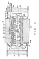
- a crimp-type semiconductor device of the present invention will be described with reference to the accompanying drawings, referring to the case where it is embodied as an anode-shorted type GTO thyristor having an alloy-free structure.
- Fig. 3 is a sectional view of the GTO thyristor embodying the present invention.
- a disk-shaped silicon semiconductor substrate 20 is made up of first and second semiconductor layers which are of the first and second conductivity types, respectively, and which are stacked upon each other. These semiconductor layers serve as base layers 21b and 21c, respectively.
- a plurality of first-conductivity type impurity regions are formed in the base layer 21b such that their surfaces are exposed.
- a plurality of second-conductivity type impurity regions are formed on the base 21c such that they are projected from the surface of the base layer 21c.
- the first- and second-conductivity type impurity regions serve as emitter layers 21a and 21d of the GTO thyristor, respectively.
- the emitter layers 21d each have a substantially rectangular shape, and are radially arranged on the disk-shaped semiconductor substrate 20 around the center of the substrate 20.
- the upper side of the semiconductor substrate 20 will be referred to as the second major surface 22 herein, and this major surface 22 is constituted by the surface of the first-conductivity type base layer 21c.
- the second-conductivity type emitter layers 21d serve as a cathode region, and a second main electrode 23 is formed on each of the emitter layers 21d.
- the first-conductivity type base layer 21c serves as a base region, and a control electrode 24 is formed on the base layer 21d.
- the lower side of the semiconductor substrate 20 will be referred to as the first major surface 21 herein, and the first-conductivity type emitter layers 21a and the second-conductivity type base layer 21b are exposed in the first major surface 21.
- a first main electrode 25 is formed on the first major surface 21, such that the emitter layers 21a and the base layer 21b are short-circuited to each other.
- the second-conductivity type emitter layers 21d are formed by doping second-conductivity type impurities, such as phosphorus, into selected portions of the first-conductivity type base layer 21c by either ion implantation or diffusion. After the impurities are diffused in the base layer 21c, the impurity-diffused regions are selectively removed by isotropic or anisotropic etching.
- second-conductivity type impurities such as phosphorus
- the second-conductivity emitter layers 21d are each in the form of an elongated segment, and are radially arranged on the base layer 21c in such a manner that they provide a plurality of concentric arrays.
- the emitter layers 21d are projected from the base layer 21c. If viewed from above, the emitter layers 21d look like a plurality of rings arranged around the control electrode 24. It should be noted that the emitter layers 21d need not be arranged in a radial pattern; they may be arranged in parallel to one another, if so desired.
- the semiconductor substrate 20 is provided with lifetime-different regions on selected portions thereof.
- the lifetime of the regions is controlled such that the ability to withstand turn-off operations, particularly turn-off operations at high frequencies, can be improved, without causing adverse effects on the gate sensitivity, the ON voltage, the turn-off characteristic and other characteristics.
- the lifetime control is carried out by the diffusion of heavy metal (e.g, gold or platinum), the irradiation of a radiation (e.g., an electron beam), or both of these in combination.
- the lifetime of the regions in question is controlled to be within the range of 10 to 35 ⁇ m or so, by the diffusion of gold or platinum and by the irradiation of an electron beam.
- the entire semiconductor substrate may be irradiated with electron beams or protons.
- a larger amount of electron beams or protons are irradiated toward that region of the semiconductor substrate 20 which indicated by the oblique lines in Fig. 4, so that the lifetime of the minority carriers in that region is shorter than the lifetime of the minority carriers in the other regions.
- the shorter-lifetime region corresponds in location to the lifetime-controlled region 43 mentioned above, and its inner diameter is equal to that of the lifetime-controlled region 43.
- a first electrode member 26 is arranged with reference to the first main electrode 25, and a second electrode member 27 is arranged with reference to both the second main electrode 23 and the control electrode 24.
- the first electrode member 26 is formed of high-melting point metal, such as W or Mo, and serves as a temperature compensation plate (i.e., a buffer plate against heat).
- the second electrode member 27 is made up of: a temperature compensation plate 28 formed of the same material as the first electrode member 26; and a soft-metal thin plate 29.
- the soft-metal thin plate 29 is a plate formed of Ag, Al or Cu.
- first electrode member 26 is outwardly projected from the outer periphery of the first main electrode 25, and the outer periphery of the second electrode member 27 is outwardly projected from the radially-outer ends of the second main electrodes 23 constituting the outermost array.
- First and second electrode posts 30 and 31 are stacked on the first and second electrode members 26 and 27, respectively, to thereby obtain a crimp-type structure.
- the first and second electrode posts 30 and 21 have outer diameters which are smaller than those of the first and second electrode members 26 and 27, respectively, and inner diameters which are greater than those of the first and second electrode members 26 and 27, respectively.
- Cutaway sections 30A and 31A are formed at the outer peripheries of the upper and lower surfaces of the first and second electrode posts 30 and 31, respectively.
- the second electrode post 31 has a groove section 32 which is formed by partly cutting out the post 31 from the center to the periphery, and members for pressing the semiconductor substrate and a gate lead 35 are arranged inside the groove section 32.
- an insulating material 33 is arranged on the groove section 32 of the second electrode post 31.
- a conductive member 36 is located at one end of the gate lead 35, and a spring member is provided for the conductive member 36. Since the conductive member 36 is pressed against the control electrode 24 by the expanding force of the spring member, the second electrode post 31 is pressed against the semiconductor substrate 20, accordingly.
- the gate lead 35 is electrically connected to the control electrode 24, and the conductive member 36 located at one end of the gate lead 35 is provided with a short-diameter straight portion 37 and an extension portion 38.
- the straight portion 37 is continuous to the conductive member 36, and the extension portion 38 is bent with reference to the straight portion 37 and is connected to a point outside of the element.
- the crimp-type power GTO element is received in a ceramic tubular envelope 39, and flanges attached to the first and second electrode posts 30 and 31 are soldered to the tubular envelope 39.
- the extension portion 38 of the gate lead 35 is covered with a metallic sleeve 40 which is inserted into and fixed to the tubular envelope 39.
- the side faces of the semiconductor substrate 20 are beveled, subjected to etching treatment, and then covered with silicone resin 41 or the like, for encapsulation. In this manner, the pn junctions exposed by beveling the side faces of the semiconductor substrate 20 are protected.
- a positioning guide 42 is used for positioning the main electrodes, the electrode members and the electrode posts with reference to one another.
- the semiconductor substrate 20 is positioned with reference to the first and second electrode members 26 and 27 by utilizing the silicon resin coated on the side faces of the semiconductor substrate 20.
- the second electrode member 27 and the second electrode post 31 are positioned with reference to each other by utilizing the positioning guide 42.
- This positioning guide 42 can also be used for positioning the gate lead 35.
- the positioning guide 42 is formed of an insulating material, such as Teflon (trademark) or epoxy resin, and is an annular member having a step section on the upper face thereof.
- the outer peripheral face of the upper portion of the positioning guide 42 has an outer diameter equal to the hollow section of the second electrode post, and the outer peripheral face of the lower portion thereof has an outer diameter equal to the hollow section of the second electrode member 27.
- the lifetime of the minority-carrier portions of the semiconductor substrate 20 is decreased to approximately to half (i.e., 5 pm to 20 pm)) by the irradiation of electron beams and protons.
- the lifetime-controlled region 43 is controlled is in the form of a ring.
- the inner diameter of this lifetime-controlled region 43 is greater than the diameter of an enveloping circle obtained by connecting the radially-inner ends of the emitter layers 21d of the outermost array.
- the inner diameter of the lifetime-controlled region 43 is smaller than the diameter of the circle along which the lower end of the cutaway section 31A of the second electrode post 31 is in contact with the second electrode member 27.
- the inner diameter of the lifetime-controlled region 23 is greater than the value obtained by subtracting the value corresponding to the thickness of the second electrode post 27 from the value corresponding to the diameter along which the lower end of the cutaway section 31A of the second electrode post 31 is in contact with the second electrode member 27.
- the GTO thyristor has a breakdown voltage in the range of 2,500 to 4,500 V, and the first-conductivity type base layer 21c initially has a specific resistance in the range of 100 to 250 ⁇ cm.
- the irradiation of electron beams and protons is carried out, with an electrode beam intensity of 5 to 15 MeV and with a dose of 5 ⁇ 10 11 to 5 ⁇ 10 12 1cm 2 .
- those regions of the semiconductor substrate 20 other than the lifetime-controlled region 43 are covered with a shield plate having a thickness of 5 to 10 mm and formed of tungst-en or molybdenum.
- the irradiation of electron beams or protons is carried out with respect to the semiconductor substrate portions whose heat-radiating characteristic is not good.
- the amount of electron beams or protons which are irradiated onto such substrate portions ranges from the value approximately equal to the amount which is irradiated over the entire semiconductor substrate to the value which is twice as large as that amount.
- a crimp-type power GTO thyristor is obtained, wherein the lifetime of its lifetime-controlled region 43 (i.e., the outermost segments of the substrate 20) is about 1/4 to 3/4 of the lifetime of the other segments of the substrate 20.
- the lifetime of part of the semiconductor substrate is reduced to a value within the predetermined range.
- the ability to withstand turn-off operations at high frequencies is improved from 2,700A (the value of the conventional device) to 3,300A or more (the value of the present invention), without the gate sensitivity (I GT , V GT , etc.), the constant ON characteristic (V TM ), the turn-off characteristic (t d , t gt ) being degraded.
- the device may break down if the current exceeds 3,300A. Even if this breakdown occurs, its location is not a peripheral portion of the device but a portion which is within the range of the electrode posts. Therefore, such a breakdown is not due to a poor heat-radiating characteristic of the device, but results from the original characteristic of the silicon semiconductor substrate.
- the lifetime-reduced region is too narrow or if the lifetime of this region is not reduced very much, the ability to withstand the turn-off operations remains unimproved. In such a case, breakdown may occur in a peripheral portion of the device, as in the prior art. Conversely, if the lifetime-reduced region is too wide or if the lifetime of this region is reduced too much, the gate sensitivity, the constant ON characteristic and the turn-off characteristic are degraded though the ability to withstand turn-off operations can be improved. In the present embodiment, therefore, the lifetime is controlled such that the segments located in the region where the heat-radiating characteristic is poor become comparatively hard to operate. By controlling the lifetime in this manner, the ability to withstand turn-off operations can be improved, without causing adverse effects on the other characteristics.
Description
- The present invention relates to a crimp-type power semiconductor device which is of an alloy-free structure wherein a semiconductor substrate and an electrode member are not soldered and which is suitable for use as a gate turn-off (GTO) thyristor, a reverse-blocking triode-thyristor (SCR) or a power transistor.
- A crimp-type semiconductor device, such as a gate turn-off thyristor (hereinafter referred to as a GTO thyristor), a reverse-blocking triode-thyristor (SCR) or a power transistor, is in general use as a power element. Such a semiconductor device (known to the applicant) will be explained with reference to Figs. 1 and 2, taking an anode-shorted GTO thyristor by way of example. In the descriptions below, the p- and n-conductivity types will be referred to as the first and second conductivity types, respectively.
- Referring to Fig. 1, a disk-shaped, silicon semiconductor substrate 1 is prepared by alternately stacking semiconductor layers of different conductivity types one upon another. Specifically, the semiconductor substrate 1 is made up of first-conductivity type emitter layers 1a, a second-conductivity type base layer 1b, a first-conductivity type base layer 1c and second-conductivity type emitter layers 1d, and these semiconductor layers 1a-1d are arranged in the order mentioned from the side of the first major surface 2 (i.e., the bottom side) to the side of the second major surface 3 (i.e., the top side). The first
major surface 2 serves as an anode region of a semiconductor element which is to be formed on the semiconductor substrate 1. In the plane of the firstmajor surface 2, the first-conductivity type emitter layers 1a and the second-conductivity type base layer 1b are exposed, thereby providing a short-circuited structure. The second-conductivity type emitter layers 1d are projected upward from the secondmajor surface 3, thereby providing a so-called mesa structure. - As is shown in Fig. 1, a second main electrode 4 is formed on top of each second-conductivity type emitter layer 1d. A control electrode 5 (i.e., a gate electrode) is formed on those surface portions of the first-conductivity type base layer 1c which are located between adjacent ones of the second-conductivity type emitter layers 1d.
- A first
main electrode 6, made of e.g. aluminum, is formed on the firstmajor surface 2 of the semiconductor substrate 1, thereby providing a so-called anode-shorted structure. - As is shown in Fig. 1, a
second electrode member 7E is arranged with reference to the second main electrodes 4 in an alloy-free state. Likewise, afirst electrode member 8 is arranged with reference to the firstmain electrode 6 in an alloy-free state. Thesecond electrode member 7E is made up of a temperature compensation plate 9 (i.e., a buffer plate against heat) and a soft-metal thin plate 10. Thetemperature compensation plate 9 is formed of high-melting point metal whose coefficient of thermal expansion is nearly equal to that of Si. For example, it is formed of W or Mo. The soft-metal thin plate 10 is formed of soft metal, such as Aℓ, Ag, or Cu. Thetemperature compensation plate 9 and the soft-metal thin plate 10 are in contact with each other, and the soft-metal thin plate 10 is in contact with the second main electrodes 4. Incidentally, the soft-metal thin plate 10 need not be a single-layer structure; it may be a laminated structure made up of a plurality of foils. - The
first electrode member 8 is formed of high-melting point metal whose coefficient of thermal expansion is nearly equal to that of Si. For example, it is formed of W or Mo. It is kept in contact with the firstmain electrode 6. A first electrode post 11 and asecond electrode post 12, each of which is formed of Cu, are laid over thefirst electrode member 8 and thetemperature compensation plate 9, respectively, such that the semiconductor substrate 1 is held in a strongly-pressed state. In Fig. 1, the first andsecond electrode posts 11 and 12 are depicted as having diameters substantially equal to those of thetemperature compensation plates second electrode posts 11 and 12 are determined such that they are equal to, or shorter than the diameter of the semiconductor substrate 1. - In order to make the strongly-pressed state of the substrate 1 satisfactory, the
second electrode member 7E is made up of two plates (namely, thetemperature compensation plate 9 and the soft-metal thin plate 10), as mentioned above. In addition, the second electrode post 11 is made to have a different shape from that of the first electrode post 11, such that aspring member 13 and a gate lead section 14 (both of which will be mentioned later) can be provided. - As is apparent from Fig. 1, the
second electrode post 12 has a step section which is formed by partly cutting out thepost 12 from the center to the periphery. Aninsulating member 15 is located at that position of the step section which corresponds to the control electrode 5. Apositioning guide 16 is located at both ends of theinsulating member 15. At one end of thegate lead section 14, aconductive member 17 whose size is determined in accordance with the shape of the control electrode 5 is located. Theconductive member 17 has a short-diameterstraight portion 18 which linearly extending upward, and anextension portion 19 which is bent at right angels to thestraight portion 18 and which extends to the outside of the device through an envelope 19-B (which is formed of ceramics or the like). At the other end of thegate lead section 14, a metallic sleeve 19-A soldered to the envelope 19-B is provided. Through this metallic sleeve 19-B, thegate lead section 14 is led to an external region. In order for the semiconductor substrate 1 (which is sandwiched between thesecond electrode member 7E and the first electrode member 8) to be pressed with a predetermined pressure, thespring member 13 is attached to the insulatingmember 15. A coil spring, a disk spring, or the like is used as thespring member 13. - The side faces of the semiconductor substrate 1 are beveled. After being subjected to etching treatment, the beveled surfaces are covered with silicone resin 19-C, for encapsulation. Finally, the flanges of the first and
second electrode posts 11 and 12 are coupled to the envelope 19-B by soldering, thereby completing the fabrication of the anode-shorted GTO thyristor. - Fig. 2A is a partial plan view of the second
major surface 3 of the semiconductor substrate 1, and conceptually illustrates the positional relationships between the second main electrodes 4 (indicated with solid lines) and the second electrode post 12 (indicated with broken lines). As can be seen from Fig. 2A, the second main electrodes 4 are formed on the respective second-conductivity type emitter layers 1d which are radially arranged on the first-conductivity type base layer 1c. - Fig. 2B illustrates a case where the second main electrodes 4 are arranged in parallel to one another. Like Fig. 2A, Fig. 2B is a partial plan view of the second
major surface 3 of the semiconductor substrate 1 and conceptually illustrates the positional relationships between the second main electrodes 4 (indicated with solid lines) and the second electrode post 12 (indicated with broken lines). Incidentally, reference symbol x indicates those portions of the second main electrodes 4 which are out of the range of thesecond electrode post 12. - As is shown in Fig. 1, the
second electrode post 12 is provided with acutaway section 12A. Thiscutaway section 12A is formed at a predetermined slanting angle at the periphery of the surface which is in contact with thesecond electrode member 7E. When thesecond electrode post 12 is strongly pressed against the second main electrodes 4, with thesecond electrode member 7E interposed, thecutaway section 12A prevents largely-different forces from being exerted to the end portions of the second main electrodes 4. - In the GTO thyristor shown in Fig. 1, the
second electrode post 12 does not have a satisfactory heat-radiating characteristic at those portions which are not pressed, with thesecond electrode member 7E interposed, against the second main electrodes 4, i.e., at the portions indicated by reference symbol x in Figs. 2A and 2B. - In addition, in the case where the second electrode post 12 and the second main electrodes 4 are arranged and positioned in the manner illustrated in Figs. 2A and 2B, a current flow occurs concentratedly at the ends of the regions on which a strong force is exerted. As a result, the ability to withstand a surging current, an excessive amount of turn-off current, etc. deteriorates.
- More specifically, the second main electrodes 4 are partly pressed by the
second electrode post 12. In other words, the second main electrodes 4 include those portions which are not pressed by thesecond electrode post 12. Due to the existence of such portions, the current produced inside the semiconductor substrate 1 flows concentratedly into the end portions of thesecond electrode post 12, increasing the electric resistance of the end portions. Further, the heat generated in the semiconductor substrate 1 is transmitted to the end portions of thesecond electrode post 12. As a result, the thermal resistance of the region Y indicated in Fig. 1 increases, resulting in insufficient heat radiation. - As may be understood from the above, heat is generated concentratedly in the region Y when the GTO thyristor is turned off. Thus, it may happen that the GTO thyristor will be damaged due to the generation of such a hot spot in the semiconductor substrate 1.
- The European Patent Application EP-A-0 098 175 relates to a pressure contact type semiconductor device comprising a number of radially extending finger-like island regions close together on a semiconductor substrate and radiating from a central part to a peripheral part thereof. The radial direction length of the semiconductor layers near the central part is less than that of those in the peripheral part, aiming at reducing the occurrence of cathode gate short circuits. Similarly as explained above such a device may also be damaged due to the generation of a hot spot in the semiconductor substrate.
- The Japanese Patent Application JP-A-58 169 972, published on January 10, 1984, relates to a gate turn-off thysistor and aims at reducing the beginning values of tail current, while restraining the increase of turn-on times and voltage drops by means of a method wherein the minority carriers of an N-base layer under the gate electrodes are reduced to a minimum.
- Accordingly, an object of the present invention is to provide a crimp-type semiconductor device of an alloy-free structure, wherein thermal destruction at a turn-off time is prevented, with the heat generation being suppressed in regions where the heat-radiating characteristics are not very good. A further object consists in providing such a crimp-type semiconductor device wherein a semiconductor substrate is held in a uniformly-pressed state.
- According to the invention, there is provided in common with EP-A-0 098 175, a crimp-type semiconductor device comprising a disk-shaped semiconductor substrate made up of semiconductor layers of first and second conductivity types and having first and second major surfaces, a plurality of substantially rectangular second-conductivity type impurity emitter regions radially arranged on the first-conductivity type semiconductor layer of the semiconductor substrate, said second-conductivity impurity regions being arranged to provide a plurality of concentric arrays and being projected from the second major surface of the semiconductor substrate, a first main electrode which is in contact with the first-conductivity type semiconductor layer of the semiconductor substrate, a plurality of second main electrodes which are in contact with the respective second-conductivity type impurity regions, a first electrode member which is in contact with the first main electrode, a second electrode member which is in contact with the second main electrodes, a first electrode post for pressing the first electrode member against the semiconductor substrate, said first electrode post being in contact with the first electrode member, and a second electrode post for pressing the second electrode member against the semiconductor substrate, said second electrode post being in contact with the second electrode member and having a cutaway section formed at the periphery of a lower surface thereof.
- The invention is characterised in that said crimp-type semiconductor device comprises a plurality of first-conductivity type impurity regions formed in the second-conductivity type semiconductor layer of the semiconductor substrate and exposed on the first major surface of the semiconductor substrate, said first electrode post has a cutaway formed at the periphery of an upper surface thereof, and said disk-shaped semiconductor substrate is provided with an annular lifetime-controlled region in said second-conductivity type impurity regions of the outermost array, the inner diameter of said lifetime-controlled region being greater than the diameter of an enveloping circle obtained by connecting radially-inner ends of the second-conductivity type impurity regions of the outermost array.
- The inner diameter of the annular lifetime region is preferably equal to, or smaller than the diameter of a circle corresponding to the lower end of the cutaway section of the second electrode post.
- In accordance with a preferred embodiment, the crimp-type power semiconductor device is an alloy-free structure wherein the semiconductor substrate and the electrode members are in direct contact with each other, with no soldering material interposed. The outer diameter of the second electrode member is greater than that of the arranging pattern of the second main electrodes, while the inner diameter of the second electrode member is smaller than that of the arranging pattern of the second main electrodes. The outer diameter of the first electrode member is greater than that of the first main electrode, so that the first electrode member covers the entire surface of the first main electrode.
- Further, the outer diameter of the first electrode post is smaller than that of the first electrode member, and the outer diameter of the second electrode post is smaller than that of the second electrode member. Therefore, the first and second electrode posts press each portion of the first and second electrode member with a uniform pressure. In general, it is considered that in a substantially flat crimp-type semiconductor device, the path of the main current and the path of the heat generated in the semiconductor substrate are substantially the same. Therefore, each of the semiconductor layers of the substrates is formed such that the region through which the main current flows in the semiconductor device is covered with the electrode members. With this structure, the density of the main current flowing through the substrate does not differ greatly from the density of the main current flowing through the main electrodes.
- Moreover, the semiconductor substrate is provided with a short-lifetime segment located in regions where the heat-radiating characteristic is not good. Since such a segment is comparatively hard to operate, the ability to withstand turn-off operations is improved, without the turn-off characteristics being degraded.
- This invention can be more fully understood from the following detailed description given by way of example and taken in conjunction with the accompanying drawings, in which:
- Fig. 1 is a schematic sectional view of a GTO thyristor which is an example of a conventional crimp-type semiconductor device;
- Figs. 2A and 2B conceptually illustrate the two positional relationships between the second-conductivity type emitter layers and second electrode post of the GTO thyristor shown in Fig. 1;
- Fig. 3 is a schematic sectional view of a GTO thyristor which is an example of a crimp-type semiconductor device according to the present invention; and
- Fig. 4 conceptually illustrates the positional relationships between the second-conductivity type emitter layers and electron beam-irradiated section of the GTO thyristor shown in Fig. 3.
- A crimp-type semiconductor device of the present invention will be described with reference to the accompanying drawings, referring to the case where it is embodied as an anode-shorted type GTO thyristor having an alloy-free structure.
- Fig. 3 is a sectional view of the GTO thyristor embodying the present invention. Referring to Fig. 3, a disk-shaped
silicon semiconductor substrate 20 is made up of first and second semiconductor layers which are of the first and second conductivity types, respectively, and which are stacked upon each other. These semiconductor layers serve as base layers 21b and 21c, respectively. A plurality of first-conductivity type impurity regions are formed in the base layer 21b such that their surfaces are exposed. A plurality of second-conductivity type impurity regions are formed on the base 21c such that they are projected from the surface of the base layer 21c. The first- and second-conductivity type impurity regions serve as emitter layers 21a and 21d of the GTO thyristor, respectively. The emitter layers 21d each have a substantially rectangular shape, and are radially arranged on the disk-shapedsemiconductor substrate 20 around the center of thesubstrate 20. - The upper side of the
semiconductor substrate 20 will be referred to as the secondmajor surface 22 herein, and thismajor surface 22 is constituted by the surface of the first-conductivity type base layer 21c. The second-conductivity type emitter layers 21d serve as a cathode region, and a second main electrode 23 is formed on each of the emitter layers 21d. The first-conductivity type base layer 21c serves as a base region, and acontrol electrode 24 is formed on thebase layer 21d. The lower side of thesemiconductor substrate 20 will be referred to as the firstmajor surface 21 herein, and the first-conductivity type emitter layers 21a and the second-conductivity type base layer 21b are exposed in the firstmajor surface 21. A firstmain electrode 25 is formed on the firstmajor surface 21, such that the emitter layers 21a and the base layer 21b are short-circuited to each other. - The second-conductivity type emitter layers 21d are formed by doping second-conductivity type impurities, such as phosphorus, into selected portions of the first-conductivity type base layer 21c by either ion implantation or diffusion. After the impurities are diffused in the base layer 21c, the impurity-diffused regions are selectively removed by isotropic or anisotropic etching.
- As is shown in Fig. 4, the second-conductivity emitter layers 21d are each in the form of an elongated segment, and are radially arranged on the base layer 21c in such a manner that they provide a plurality of concentric arrays. The emitter layers 21d are projected from the base layer 21c. If viewed from above, the emitter layers 21d look like a plurality of rings arranged around the
control electrode 24. It should be noted that the emitter layers 21d need not be arranged in a radial pattern; they may be arranged in parallel to one another, if so desired. - The
semiconductor substrate 20 is provided with lifetime-different regions on selected portions thereof. The lifetime of the regions is controlled such that the ability to withstand turn-off operations, particularly turn-off operations at high frequencies, can be improved, without causing adverse effects on the gate sensitivity, the ON voltage, the turn-off characteristic and other characteristics. In general, the lifetime control is carried out by the diffusion of heavy metal (e.g, gold or platinum), the irradiation of a radiation (e.g., an electron beam), or both of these in combination. The lifetime of the regions in question is controlled to be within the range of 10 to 35 µm or so, by the diffusion of gold or platinum and by the irradiation of an electron beam. - The entire semiconductor substrate may be irradiated with electron beams or protons. In this case, a larger amount of electron beams or protons are irradiated toward that region of the
semiconductor substrate 20 which indicated by the oblique lines in Fig. 4, so that the lifetime of the minority carriers in that region is shorter than the lifetime of the minority carriers in the other regions. The shorter-lifetime region corresponds in location to the lifetime-controlledregion 43 mentioned above, and its inner diameter is equal to that of the lifetime-controlledregion 43. - Next, a description will be given as to how the crimp-type semiconductor device incorporating the above-described semiconductor substrate is assembled. A
first electrode member 26 is arranged with reference to the firstmain electrode 25, and asecond electrode member 27 is arranged with reference to both the second main electrode 23 and thecontrol electrode 24. Thefirst electrode member 26 is formed of high-melting point metal, such as W or Mo, and serves as a temperature compensation plate (i.e., a buffer plate against heat). Thesecond electrode member 27 is made up of: atemperature compensation plate 28 formed of the same material as thefirst electrode member 26; and a soft-metal thin plate 29. The soft-metal thin plate 29 is a plate formed of Ag, Aℓ or Cu. Alternatively, it may be a laminated structure wherein foils of at least one of Ag, Aℓ and Cu are stacked upon one another. The outer periphery of thefirst electrode member 26 is outwardly projected from the outer periphery of the firstmain electrode 25, and the outer periphery of thesecond electrode member 27 is outwardly projected from the radially-outer ends of the second main electrodes 23 constituting the outermost array. First and second electrode posts 30 and 31 are stacked on the first andsecond electrode members second electrode members second electrode members Cutaway sections second electrode post 31 has agroove section 32 which is formed by partly cutting out thepost 31 from the center to the periphery, and members for pressing the semiconductor substrate and a gate lead 35 are arranged inside thegroove section 32. In order to electrically insulate thesecond electrode post 31 and thecontrol electrode 24, an insulatingmaterial 33 is arranged on thegroove section 32 of thesecond electrode post 31. Aconductive member 36 is located at one end of the gate lead 35, and a spring member is provided for theconductive member 36. Since theconductive member 36 is pressed against thecontrol electrode 24 by the expanding force of the spring member, thesecond electrode post 31 is pressed against thesemiconductor substrate 20, accordingly. - The gate lead 35 is electrically connected to the
control electrode 24, and theconductive member 36 located at one end of the gate lead 35 is provided with a short-diameterstraight portion 37 and an extension portion 38. Thestraight portion 37 is continuous to theconductive member 36, and the extension portion 38 is bent with reference to thestraight portion 37 and is connected to a point outside of the element. The crimp-type power GTO element is received in a ceramictubular envelope 39, and flanges attached to the first and second electrode posts 30 and 31 are soldered to thetubular envelope 39. As is shown in Fig. 3, the extension portion 38 of the gate lead 35 is covered with ametallic sleeve 40 which is inserted into and fixed to thetubular envelope 39. In order to maintain the breakdown voltage of the element at a predetermined value, the side faces of thesemiconductor substrate 20 are beveled, subjected to etching treatment, and then covered withsilicone resin 41 or the like, for encapsulation. In this manner, the pn junctions exposed by beveling the side faces of thesemiconductor substrate 20 are protected. - A
positioning guide 42 is used for positioning the main electrodes, the electrode members and the electrode posts with reference to one another. Specifically, thesemiconductor substrate 20 is positioned with reference to the first andsecond electrode members semiconductor substrate 20. Thesecond electrode member 27 and thesecond electrode post 31 are positioned with reference to each other by utilizing thepositioning guide 42. Thispositioning guide 42 can also be used for positioning the gate lead 35. Thepositioning guide 42 is formed of an insulating material, such as Teflon (trademark) or epoxy resin, and is an annular member having a step section on the upper face thereof. The outer peripheral face of the upper portion of thepositioning guide 42 has an outer diameter equal to the hollow section of the second electrode post, and the outer peripheral face of the lower portion thereof has an outer diameter equal to the hollow section of thesecond electrode member 27. - After the beveling and encapsulation steps which are carried out prior to the assembly of the gate lead 35, the lifetime of the minority-carrier portions of the
semiconductor substrate 20 is decreased to approximately to half (i.e., 5 pm to 20 pm)) by the irradiation of electron beams and protons. As is shown in Fig. 4, the lifetime-controlledregion 43 is controlled is in the form of a ring. The inner diameter of this lifetime-controlledregion 43 is greater than the diameter of an enveloping circle obtained by connecting the radially-inner ends of the emitter layers 21d of the outermost array. Further, the inner diameter of the lifetime-controlledregion 43 is smaller than the diameter of the circle along which the lower end of thecutaway section 31A of thesecond electrode post 31 is in contact with thesecond electrode member 27. Preferably, the inner diameter of the lifetime-controlled region 23 is greater than the value obtained by subtracting the value corresponding to the thickness of thesecond electrode post 27 from the value corresponding to the diameter along which the lower end of thecutaway section 31A of thesecond electrode post 31 is in contact with thesecond electrode member 27. - The GTO thyristor has a breakdown voltage in the range of 2,500 to 4,500 V, and the first-conductivity type base layer 21c initially has a specific resistance in the range of 100 to 250 Ω·cm. To obtain a lifetime of 5 to 20 ps, the irradiation of electron beams and protons is carried out, with an electrode beam intensity of 5 to 15 MeV and with a dose of 5 × 10¹¹ to 5 × 10¹² 1cm2.
- During the above irradiation, those regions of the
semiconductor substrate 20 other than the lifetime-controlledregion 43 are covered with a shield plate having a thickness of 5 to 10 mm and formed of tungst-en or molybdenum. In other words, the irradiation of electron beams or protons is carried out with respect to the semiconductor substrate portions whose heat-radiating characteristic is not good. The amount of electron beams or protons which are irradiated onto such substrate portions ranges from the value approximately equal to the amount which is irradiated over the entire semiconductor substrate to the value which is twice as large as that amount. - As a result of the above irradiation, a crimp-type power GTO thyristor is obtained, wherein the lifetime of its lifetime-controlled region 43 (i.e., the outermost segments of the substrate 20) is about 1/4 to 3/4 of the lifetime of the other segments of the
substrate 20. - As mentioned above, the lifetime of part of the semiconductor substrate is reduced to a value within the predetermined range. As a result of the reduced lifetime, the ability to withstand turn-off operations at high frequencies is improved from 2,700A (the value of the conventional device) to 3,300A or more (the value of the present invention), without the gate sensitivity (IGT, VGT, etc.), the constant ON characteristic (VTM), the turn-off characteristic (td, tgt) being degraded. The device may break down if the current exceeds 3,300A. Even if this breakdown occurs, its location is not a peripheral portion of the device but a portion which is within the range of the electrode posts. Therefore, such a breakdown is not due to a poor heat-radiating characteristic of the device, but results from the original characteristic of the silicon semiconductor substrate.
- If the lifetime-reduced region is too narrow or if the lifetime of this region is not reduced very much, the ability to withstand the turn-off operations remains unimproved. In such a case, breakdown may occur in a peripheral portion of the device, as in the prior art. Conversely, if the lifetime-reduced region is too wide or if the lifetime of this region is reduced too much, the gate sensitivity, the constant ON characteristic and the turn-off characteristic are degraded though the ability to withstand turn-off operations can be improved. In the present embodiment, therefore, the lifetime is controlled such that the segments located in the region where the heat-radiating characteristic is poor become comparatively hard to operate. By controlling the lifetime in this manner, the ability to withstand turn-off operations can be improved, without causing adverse effects on the other characteristics.
- Reference signs in the claims are intended for better understanding and shall not limit the scope.
Claims (2)
- A crimp-type semiconductor device comprising:a disk-shaped semiconductor substrate (20) made up of semiconductor layers (21b, 21c) of first and second conductivity types (P,N) and having first and second major surfaces (21, 22);a plurality of substantially rectangular second-conductivity type impurity emitter regions (21d) radially arranged on the first-conductivity type semiconductor layer (21c) of the semiconductor substrate (20), said second-conductivity impurity regions (21d) being arranged to provide a plurality of concentric arrays and being projected from the second major surface (22) of the semiconductor substrate (20);a first main electrode (25) which is in contact with the first-conductivity type semiconductor layer (21b) of the semiconductor substrate (20);a plurality of second main electrodes (23) which are in contact with the respective second-conductivity type impurity regions (21d);a first electrode member (26) which is in contact with the first main electrode (25);a second electrode member (27) which is in contact with the second main electrodes (23);a first electrode post (30) for pressing the first electrode member (26) against the semiconductor substrate (20), said first electrode post (30) being in contact with the first electrode member (26); anda second electrode post (31) for pressing the second electrode member (27) against the semiconductor substrate (20), said second electrode post (31) being in contact with the second electrode member (27) and having a cutaway section (31A) formed at the periphery of a lower surface thereof,characterized in thatsaid crimp-type semiconductor device comprises a plurality of first-conductivity type impurity regions (21a) formed in the second-conductivity type semiconductor layer (21b) of the semiconductor substrate (20) and exposed on the first major surface (21) of the semiconductor substrate (20);said first electrode post (30) has a cutaway (30A) formed at the periphery of an upper surface thereof; andsaid disk-shaped semiconductor substrate (20) is provided with an annular lifetime-controlled region (43) in said second-conductivity type impurity regions (21d) of the outermost array, the inner diameter of said lifetime-controlled region (43) being greater than the diameter of an enveloping circle obtained by connecting radially-inner ends of the second-conductivity type impurity regions (21d) of the outermost array.
- A crimp-type semiconductor device according to claim 1, characterized in that the inner diameter of said lifetime-controlled region (43) is equal to, or smaller than the diameter of a circle along which the lower end of the cutaway section (31A) of the second electrode post (31) is in contact with the second electrode member (27).
Applications Claiming Priority (2)
| Application Number | Priority Date | Filing Date | Title |
|---|---|---|---|
| JP257412/89 | 1989-10-02 | ||
| JP25741289A JPH0680818B2 (en) | 1989-10-02 | 1989-10-02 | Power pressure contact type semiconductor device |
Publications (2)
| Publication Number | Publication Date |
|---|---|
| EP0421344A1 EP0421344A1 (en) | 1991-04-10 |
| EP0421344B1 true EP0421344B1 (en) | 1997-12-10 |
Family
ID=17306019
Family Applications (1)
| Application Number | Title | Priority Date | Filing Date |
|---|---|---|---|
| EP19900118866 Expired - Lifetime EP0421344B1 (en) | 1989-10-02 | 1990-10-02 | Crimp-type power semiconductor device |
Country Status (5)
| Country | Link |
|---|---|
| US (1) | US5198882A (en) |
| EP (1) | EP0421344B1 (en) |
| JP (1) | JPH0680818B2 (en) |
| KR (1) | KR940008217B1 (en) |
| DE (1) | DE69031796T2 (en) |
Families Citing this family (12)
| Publication number | Priority date | Publication date | Assignee | Title |
|---|---|---|---|---|
| EP0514615B1 (en) * | 1991-05-23 | 1995-05-03 | STMicroelectronics S.r.l. | Electronic power device realized by a series of elementary semi-conductor components connected in parallel and related manufacturing process |
| JP2804216B2 (en) * | 1993-06-22 | 1998-09-24 | 株式会社日立製作所 | Gate turn-off thyristor |
| DE69321966T2 (en) * | 1993-12-24 | 1999-06-02 | Cons Ric Microelettronica | Power semiconductor device |
| DE69321965T2 (en) * | 1993-12-24 | 1999-06-02 | Cons Ric Microelettronica | MOS power chip type and package assembly |
| US5652467A (en) * | 1995-07-27 | 1997-07-29 | Hitachi, Ltd. | Semiconductor device and package structure therefore and power inverter having semiconductor device |
| DE19800469A1 (en) * | 1998-01-09 | 1999-07-15 | Asea Brown Boveri | Low inductively controlled, gate controlled thyristor |
| US7485920B2 (en) * | 2000-06-14 | 2009-02-03 | International Rectifier Corporation | Process to create buried heavy metal at selected depth |
| DE102004058946B4 (en) * | 2004-12-08 | 2009-06-18 | Semikron Elektronik Gmbh & Co. Kg | Power semiconductor module with auxiliary connection |
| TWI344469B (en) | 2005-04-07 | 2011-07-01 | Nippon Catalytic Chem Ind | Polyacrylic acid (salt) water-absorbent resin, production process thereof, and acrylic acid used in polymerization for production of water-absorbent resin |
| EP1837348B9 (en) | 2006-03-24 | 2020-01-08 | Nippon Shokubai Co.,Ltd. | Water-absorbing resin and method for manufacturing the same |
| CN102548654A (en) | 2009-09-29 | 2012-07-04 | 株式会社日本触媒 | Particulate water absorbent and process for production thereof |
| JP7232811B2 (en) * | 2017-07-13 | 2023-03-03 | ヒタチ・エナジー・スウィツァーランド・アクチェンゲゼルシャフト | Bypass thyristor device with gas expansion cavity in contact plate |
Family Cites Families (9)
| Publication number | Priority date | Publication date | Assignee | Title |
|---|---|---|---|---|
| GB1124176A (en) * | 1966-02-24 | 1968-08-21 | Licentia Gmbh | Improvements in semiconductor switching devices |
| JPS5871658A (en) * | 1981-10-23 | 1983-04-28 | Toshiba Corp | Pressure contact type semiconductor device |
| JPS58169972A (en) * | 1982-03-31 | 1983-10-06 | Toshiba Corp | Semiconductor device |
| JPS594033A (en) * | 1982-06-30 | 1984-01-10 | Toshiba Corp | Pressure welding type semiconductor device |
| JPH0691246B2 (en) * | 1985-09-02 | 1994-11-14 | 株式会社日立製作所 | Semiconductor device |
| US4752818A (en) * | 1985-09-28 | 1988-06-21 | Kabushiki Kaisha Toyota Chuo Kenkyusho | Semiconductor device with multiple recombination center layers |
| JPS62163371A (en) * | 1986-01-13 | 1987-07-20 | Mitsubishi Electric Corp | Gate turnoff thyristor |
| JPS6358376A (en) * | 1986-08-29 | 1988-03-14 | Fuji Xerox Co Ltd | Image recording method |
| JPH07107935B2 (en) * | 1988-02-04 | 1995-11-15 | 株式会社東芝 | Semiconductor device |
-
1989
- 1989-10-02 JP JP25741289A patent/JPH0680818B2/en not_active Expired - Lifetime
-
1990
- 1990-09-28 US US07/589,600 patent/US5198882A/en not_active Expired - Lifetime
- 1990-09-29 KR KR1019900015708A patent/KR940008217B1/en not_active IP Right Cessation
- 1990-10-02 DE DE1990631796 patent/DE69031796T2/en not_active Expired - Fee Related
- 1990-10-02 EP EP19900118866 patent/EP0421344B1/en not_active Expired - Lifetime
Also Published As
| Publication number | Publication date |
|---|---|
| US5198882A (en) | 1993-03-30 |
| JPH0680818B2 (en) | 1994-10-12 |
| EP0421344A1 (en) | 1991-04-10 |
| DE69031796D1 (en) | 1998-01-22 |
| KR940008217B1 (en) | 1994-09-08 |
| DE69031796T2 (en) | 1998-04-23 |
| JPH03119762A (en) | 1991-05-22 |
| KR910008860A (en) | 1991-05-31 |
Similar Documents
| Publication | Publication Date | Title |
|---|---|---|
| US4996586A (en) | Crimp-type semiconductor device having non-alloy structure | |
| US4542398A (en) | Semiconductor devices of multi-emitter type | |
| US7635892B2 (en) | Semiconductor device | |
| EP0421344B1 (en) | Crimp-type power semiconductor device | |
| US5510634A (en) | Insulated gate bipolar transistor | |
| EP0022355B1 (en) | Gate turn-off thyristor | |
| US4835119A (en) | Semiconductor device and a process of producing same | |
| CA1201215A (en) | Gate turn-off thyristor | |
| EP0064231B1 (en) | Compression-type semiconductor device | |
| US4843449A (en) | Controllable power semiconductor | |
| US5021855A (en) | Gate turn-off thyristor | |
| US5210601A (en) | Compression contacted semiconductor device and method for making of the same | |
| JPS6156628B2 (en) | ||
| JP3883591B2 (en) | Turn-off possible semiconductor device | |
| US5248622A (en) | Finely controlled semiconductor device and method of manufacturing the same | |
| EP0366916B1 (en) | Shorted-anode semiconductor device and methods of making the same | |
| JPS6154262B2 (en) | ||
| JPH0142498B2 (en) | ||
| US11824091B2 (en) | Integrated gate-commutated thyristor (IGCT) | |
| EP0428916B1 (en) | Compression contacted semiconductor device and method for making of the same | |
| JP2000058814A (en) | Semiconductor element | |
| JPH09298292A (en) | Semiconductor device | |
| JPH09312305A (en) | Semiconductor device and cold welded semiconductor device | |
| JPH03244158A (en) | Pressure weld type power semiconductor element | |
| JPS592189B2 (en) | reverse conducting thyristor |
Legal Events
| Date | Code | Title | Description |
|---|---|---|---|
| PUAI | Public reference made under article 153(3) epc to a published international application that has entered the european phase |
Free format text: ORIGINAL CODE: 0009012 |
|
| 17P | Request for examination filed |
Effective date: 19901002 |
|
| AK | Designated contracting states |
Kind code of ref document: A1 Designated state(s): CH DE FR GB LI SE |
|
| 17Q | First examination report despatched |
Effective date: 19940630 |
|
| GRAG | Despatch of communication of intention to grant |
Free format text: ORIGINAL CODE: EPIDOS AGRA |
|
| GRAH | Despatch of communication of intention to grant a patent |
Free format text: ORIGINAL CODE: EPIDOS IGRA |
|
| GRAH | Despatch of communication of intention to grant a patent |
Free format text: ORIGINAL CODE: EPIDOS IGRA |
|
| GRAA | (expected) grant |
Free format text: ORIGINAL CODE: 0009210 |
|
| AK | Designated contracting states |
Kind code of ref document: B1 Designated state(s): CH DE FR GB LI SE |
|
| REG | Reference to a national code |
Ref country code: CH Ref legal event code: EP Ref country code: CH Ref legal event code: NV Representative=s name: E. BLUM & CO. PATENTANWAELTE |
|
| REF | Corresponds to: |
Ref document number: 69031796 Country of ref document: DE Date of ref document: 19980122 |
|
| ET | Fr: translation filed | ||
| REG | Reference to a national code |
Ref country code: GB Ref legal event code: 746 Effective date: 19980910 |
|
| PLBE | No opposition filed within time limit |
Free format text: ORIGINAL CODE: 0009261 |
|
| STAA | Information on the status of an ep patent application or granted ep patent |
Free format text: STATUS: NO OPPOSITION FILED WITHIN TIME LIMIT |
|
| 26N | No opposition filed | ||
| REG | Reference to a national code |
Ref country code: FR Ref legal event code: D6 |
|
| REG | Reference to a national code |
Ref country code: GB Ref legal event code: IF02 |
|
| REG | Reference to a national code |
Ref country code: CH Ref legal event code: PFA Owner name: KABUSHIKI KAISHA TOSHIBA Free format text: KABUSHIKI KAISHA TOSHIBA#72, HORIKAWA-CHO, SAIWAI-KU#KAWASAKI-SHI, KANAGAWA-KEN 210 (JP) -TRANSFER TO- KABUSHIKI KAISHA TOSHIBA#72, HORIKAWA-CHO, SAIWAI-KU#KAWASAKI-SHI, KANAGAWA-KEN 210 (JP) |
|
| PGFP | Annual fee paid to national office [announced via postgrant information from national office to epo] |
Ref country code: CH Payment date: 20070927 Year of fee payment: 18 |
|
| PGFP | Annual fee paid to national office [announced via postgrant information from national office to epo] |
Ref country code: GB Payment date: 20070926 Year of fee payment: 18 |
|
| PGFP | Annual fee paid to national office [announced via postgrant information from national office to epo] |
Ref country code: DE Payment date: 20070927 Year of fee payment: 18 |
|
| PGFP | Annual fee paid to national office [announced via postgrant information from national office to epo] |
Ref country code: SE Payment date: 20071004 Year of fee payment: 18 |
|
| PGFP | Annual fee paid to national office [announced via postgrant information from national office to epo] |
Ref country code: FR Payment date: 20071009 Year of fee payment: 18 |
|
| REG | Reference to a national code |
Ref country code: CH Ref legal event code: PL |
|
| EUG | Se: european patent has lapsed | ||
| GBPC | Gb: european patent ceased through non-payment of renewal fee |
Effective date: 20081002 |
|
| REG | Reference to a national code |
Ref country code: FR Ref legal event code: ST Effective date: 20090630 |
|
| PG25 | Lapsed in a contracting state [announced via postgrant information from national office to epo] |
Ref country code: DE Free format text: LAPSE BECAUSE OF NON-PAYMENT OF DUE FEES Effective date: 20090501 |
|
| PG25 | Lapsed in a contracting state [announced via postgrant information from national office to epo] |
Ref country code: FR Free format text: LAPSE BECAUSE OF NON-PAYMENT OF DUE FEES Effective date: 20081031 Ref country code: CH Free format text: LAPSE BECAUSE OF NON-PAYMENT OF DUE FEES Effective date: 20081031 Ref country code: LI Free format text: LAPSE BECAUSE OF NON-PAYMENT OF DUE FEES Effective date: 20081031 |
|
| PG25 | Lapsed in a contracting state [announced via postgrant information from national office to epo] |
Ref country code: GB Free format text: LAPSE BECAUSE OF NON-PAYMENT OF DUE FEES Effective date: 20081002 |
|
| PG25 | Lapsed in a contracting state [announced via postgrant information from national office to epo] |
Ref country code: SE Free format text: LAPSE BECAUSE OF NON-PAYMENT OF DUE FEES Effective date: 20081003 |