EP0433054A2 - A driving circuit of a liquid crystal display - Google Patents
A driving circuit of a liquid crystal display Download PDFInfo
- Publication number
- EP0433054A2 EP0433054A2 EP90313541A EP90313541A EP0433054A2 EP 0433054 A2 EP0433054 A2 EP 0433054A2 EP 90313541 A EP90313541 A EP 90313541A EP 90313541 A EP90313541 A EP 90313541A EP 0433054 A2 EP0433054 A2 EP 0433054A2
- Authority
- EP
- European Patent Office
- Prior art keywords
- circuit
- signals
- bits
- video signals
- line
- Prior art date
- Legal status (The legal status is an assumption and is not a legal conclusion. Google has not performed a legal analysis and makes no representation as to the accuracy of the status listed.)
- Granted
Links
Images


Classifications
-
- G—PHYSICS
- G09—EDUCATION; CRYPTOGRAPHY; DISPLAY; ADVERTISING; SEALS
- G09G—ARRANGEMENTS OR CIRCUITS FOR CONTROL OF INDICATING DEVICES USING STATIC MEANS TO PRESENT VARIABLE INFORMATION
- G09G3/00—Control arrangements or circuits, of interest only in connection with visual indicators other than cathode-ray tubes
- G09G3/20—Control arrangements or circuits, of interest only in connection with visual indicators other than cathode-ray tubes for presentation of an assembly of a number of characters, e.g. a page, by composing the assembly by combination of individual elements arranged in a matrix no fixed position being assigned to or needed to be assigned to the individual characters or partial characters
- G09G3/34—Control arrangements or circuits, of interest only in connection with visual indicators other than cathode-ray tubes for presentation of an assembly of a number of characters, e.g. a page, by composing the assembly by combination of individual elements arranged in a matrix no fixed position being assigned to or needed to be assigned to the individual characters or partial characters by control of light from an independent source
- G09G3/36—Control arrangements or circuits, of interest only in connection with visual indicators other than cathode-ray tubes for presentation of an assembly of a number of characters, e.g. a page, by composing the assembly by combination of individual elements arranged in a matrix no fixed position being assigned to or needed to be assigned to the individual characters or partial characters by control of light from an independent source using liquid crystals
- G09G3/3611—Control of matrices with row and column drivers
- G09G3/3685—Details of drivers for data electrodes
- G09G3/3688—Details of drivers for data electrodes suitable for active matrices only
-
- G—PHYSICS
- G09—EDUCATION; CRYPTOGRAPHY; DISPLAY; ADVERTISING; SEALS
- G09G—ARRANGEMENTS OR CIRCUITS FOR CONTROL OF INDICATING DEVICES USING STATIC MEANS TO PRESENT VARIABLE INFORMATION
- G09G2310/00—Command of the display device
- G09G2310/02—Addressing, scanning or driving the display screen or processing steps related thereto
- G09G2310/0264—Details of driving circuits
- G09G2310/027—Details of drivers for data electrodes, the drivers handling digital grey scale data, e.g. use of D/A converters
-
- G—PHYSICS
- G09—EDUCATION; CRYPTOGRAPHY; DISPLAY; ADVERTISING; SEALS
- G09G—ARRANGEMENTS OR CIRCUITS FOR CONTROL OF INDICATING DEVICES USING STATIC MEANS TO PRESENT VARIABLE INFORMATION
- G09G3/00—Control arrangements or circuits, of interest only in connection with visual indicators other than cathode-ray tubes
- G09G3/20—Control arrangements or circuits, of interest only in connection with visual indicators other than cathode-ray tubes for presentation of an assembly of a number of characters, e.g. a page, by composing the assembly by combination of individual elements arranged in a matrix no fixed position being assigned to or needed to be assigned to the individual characters or partial characters
- G09G3/2007—Display of intermediate tones
- G09G3/2011—Display of intermediate tones by amplitude modulation
-
- G—PHYSICS
- G09—EDUCATION; CRYPTOGRAPHY; DISPLAY; ADVERTISING; SEALS
- G09G—ARRANGEMENTS OR CIRCUITS FOR CONTROL OF INDICATING DEVICES USING STATIC MEANS TO PRESENT VARIABLE INFORMATION
- G09G3/00—Control arrangements or circuits, of interest only in connection with visual indicators other than cathode-ray tubes
- G09G3/20—Control arrangements or circuits, of interest only in connection with visual indicators other than cathode-ray tubes for presentation of an assembly of a number of characters, e.g. a page, by composing the assembly by combination of individual elements arranged in a matrix no fixed position being assigned to or needed to be assigned to the individual characters or partial characters
- G09G3/2007—Display of intermediate tones
- G09G3/2014—Display of intermediate tones by modulation of the duration of a single pulse during which the logic level remains constant
Definitions
- the present invention relates to a driving circuit for driving source lines of an active-matrix type liquid crystal display having a thin film transistor matrix array (TFT array).
- TFT array thin film transistor matrix array
- the reference numeral 21 denotes a timing generating circuit.
- the timing generating circuit 21 receives horizontal and vertical synchronizing signals HD and VD as reference timing signals.
- the horizontal and vertical synchronizing signals HD and VD are synchronized with analog video signals to be described below.
- a shift register circuit 22 receives sampling clocks CK and start pulses P ST from the timing generating circuit 21.
- Analog video signals SVa are supplied to a sampling gate circuit 23.
- the gate circuit 23 has a plurality of gate portions.
- the gate portions sample the video signals Sva to obtain pixel signals.
- the gate portions receive gate pulses P SG from the shift register circuit 22 to sample the pixel signals for one line for each horizontal period.
- a latch gate circuit 24 receives the pixel signals for one line which are sampled by the gate circuit 23.
- Latch pulses P LG are supplied from the timing generating circuit 21 to the gate circuit 24 for a horizontal blanking period. Consequently, the pixel signals for one line supplied from the gate circuit 23 are latched and held for a next horizontal period.
- the pixel signals for one line outputted from the gate circuit 24 are simultaneously supplied to corresponding source lines ls of a TFT array 10 through an output circuit 25.
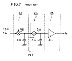
- Fig. 7 is a diagram showing a specific partial construction of the gate circuits 23 and 24 and the output circuit 25 corresponding to one pixel signal.
- the whole of the gate circuits 23 and 24 and the output circuit 25 consists of the predetermined number of the above constructions.
- the reference numerals G23 and G24 denote gates.
- the reference numerals C23 and C24 denote capacitors.
- the reference numeral A25 denotes a buffer.
- the timing generating circuit 21 supplies control signals to a gate driving circuit 26. Then, scanning pulses are sequentially supplied to gate lines lg.
- the gate lines lg are arranged in positions corresponding to the pixel signals for one line which are supplied to the source lines ls of the TFT array 10 through the output circuit 25.
- the analog video signals SVa are inputted. Therefore, if the number of pixels for one line is increased like the TFT array 10 having a large screen and high quality of image, a sampling time which is allowed for one pixel signal. becomes shorter. Consequently, the time for charging the capacitor C23 of the gate circuit 23 becomes insufficient so that the video signals SVa cannot be sampled accurately. In other words, the TFT array 10 cannot accurately be driven corresponding to the video signals SVa. Therefore, it is difficult to obtain the good quality of display.
- Japanese Unexamined Patent Publication Nos. 63-182695 and 63-186295 have disclosed a circuit for driving the liquid crystal display in response to digital video signals.
- a driving circuit for selecting driving voltages corresponding to inputted multigradation digital video signals to output the same to the liquid crystal display.
- a driving circuit for receiving data which specifies a display brightness for each pixel of the liquid crystal display on the basis of a value represented by a plurality of bits and then outputting a driving signal having a pulse width corresponding to the data.
- the present invention provides a driving circuit of a liquid crystal display for driving source lines of an active-matrix type liquid crystal display having a thin film transistor matrix array comprising a shift register circuit for sequentially storing digital video signals for one line, each of the digital video signals being comprised of pixel data of a series of predetermined bits, a latch circuit for holding for one horizontal period the digital video signals for one line stored in the shift register circuit, a conversion circuit for classifying each pixel data constituting the digital video signals for one line outputted from the latch circuit into upper and lower bits, selecting adjacent two different DC voltages according to a value designated by the upper bits, performing pulse width modulation between the two different DC voltages according to a value designated by the lower bits and supplying analog video signals to the corresponding source lines of the matrix array, and a comparison data generating circuit for outputting comparison data which has bits by number equal to that of the lower bits and is compared with the lower bits to the conversion circuit.
- Fig. 1 is a block diagram showing one embodiment of the present invention
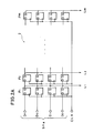
- Figs. 2A and B are circuit diagrams showing constructions of a shift register circuit, a latch circuit and a conversion circuit
- Fig. 3 is a circuit diagram showing the conversion circuit of the embodiment
- Figs. 4A, B and C are diagrams for explaining an operation of the conversion circuit
- Fig. 5 is a circuit diagram of a comparison data generator and a pulse width modulator of the embodiment
- Fig. 6 is a block diagram of a conventional example.
- Fig. 7 is a circuit diagram of a main portion of the conventional example.
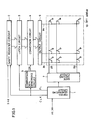
- a driving circuit of a liquid crystal display comprises a timing generating circuit, a gate driving circuit, an output circuit and a power circuit basically.
- the timing generating circuit outputs signals for judging a timing of signal processing.
- the gate driving circuit drives gate lines of a thin film transistor matrix array (TFT array) of an active-matrix type liquid crystal display to be driven.
- the output circuit properly levels analog video signals to be supplied to source lines of the TFT array.
- the power circuit outputs DC voltages.
- digital video signals for one line are sequentially stored in a shift register circuit, held by a latch circuit for one horizontal period and then converted into the analog video signals by a conversion circuit so as to be supplied to the source lines of the TFT array.
- a processing in which pixel signals are sampled from the analog video signals is not performed. Consequently, even if the number of pixels for one line is increased, the TFT array can sufficiently and accurately be driven corresponding to the video signals.
- An example of an active-matrix type liquid crystal display which can be driven by the driving circuit of the present invention is such that pixel electrodes are formed like a matrix in a liquid crystal cell and thin film transistors are respectively connected to the respective pixel electrodes in order to or not to apply voltages thereto so that a thin film transistor matrix array is formed (for example, Japanese Unexamined Patent Publication No. 59492/1986).
- the reference numeral 1 denotes a timing generating circuit.
- the timing generating circuit 1 receives horizontal and vertical synchronizing signals HD and VD as reference timing signals.
- the horizontal and vertical synchronizing signals HD and VD are synchronized with digital video signals SVd to be described below.
- the reference numeral 2 denotes a shift register circuit.
- the shift register circuit 2 sequentially stores the digital video signals for one line which are comprised of pixel data of a series of predetermined bits.
- the shift register circuit 2 receives the digital video signals SVd.
- the digital video signal SVd is comprised of pixel data Pl to Pm which have 8 bits of D0 to D7 respectively.
- the shift register circuit 2 receives clocks CLK from the timing generating circuit 1 and sequentially stores the digital video signals SVd for one line for each horizontal period (see Fig. 2A).
- a latch circuit 3 receives the pixel data for one line which are stored in the shift register circuit 2 for each horizontal period (see Fig. 2B). Latch pulses PL are supplied from the timing generating circuit 1 to the latch circuit 3 for a horizontal blanking period so that the pixel data (Ll to Lm) for one line supplied from the shift register circuit 2 are latched and held for a next horizontal period.
- a conversion circuit 4 receives the pixel data for one line outputted from the latch circuit 3.
- the conversion circuit 4 classifies each pixel data which forms the digital video signals for one line outputted from the latch circuit 3 into upper bits and lower bits respectively, and then selects adjacent two different DC voltages according to a value designated by the upper bits and performs pulse width modulation between the two different DC voltages according to a value designated by the lower bits to supply the analog video signals to the corresponding source lines of the matrix array.
- the conversion circuit 4 classifies each pixel data of 8 bits into data DH (D7 to D4) of the upper 4 bits and data DL (D3 to D0) of the lower 4 bits respectively.
- the data DH of the upper 4 bits selects adjacent two different voltages VA and VB which are supplied to the source lines of the TFT array 10 among voltages V0 (Vmin), V1, V2, ..., V16 (Vmax).
- the voltages V0 (Vmin), V1, V2, ..., V16 (Vmax) are provided at equal intervals between maximum and minimum voltages Vmax and Vmin.
- n 0 to 15
- VA Vn+1
- VB Vn.
- the pulse width modulation is executed between the voltages VA and VB selected according to the date DL of the lower bits as described above. Then, pulse width modulation signals are integrated and outputted.
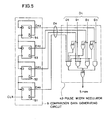
- the conversion circuit 4 includes unit circuits 41, 42,..., 4m which correspond to the number of the pixel data for one line (see Fig. 2B). As shown in Fig. 3, each unit circuit has a switching circuit 41, a pulse width modulator 43, two switching elements 42N and 42P, and an integrating circuit 44.
- the switching circuit 41 selects the DC voltages.
- the pulse width modulator 43 compares the lower bits with comparison data DR outputted from a comparison data generating circuit 5 so as to output signals having different pulse widths corresponding to the result of comparison.
- the switching elements 42N and 42P switch the DC voltages outputted from the switching circuit 41 in response to the signals outputted from the pulse width modulator 43.
- the integrating circuit 44 outputs the analog pixel signals in response to the signals outputted from the switching elements 42N and 42P.
- Fig. 3 is a diagram showing a construction of one pixel portion of the conversion circuit 4.
- the switching circuit 41 receives the voltages V0 to V16, selects and outputs the voltages VA and VB according to the data DH of the upper 4 bits (see Fig. 4A).
- the voltages VA and VB selected by the switching circuit 41 are supplied to a drain of an N-channel FET (field effect transistor) 42N and to a source of a P-channel FET 42P respectively.
- the reference numeral 43 denotes a pulse width modulator.
- the pulse width modulator 43 receives the data DL of the lower 4 bits and the comparison data DR (DR3 to DR0) of 4 bits from the comparison data generating circuit 5 (see Fig. 1).
- the comparison data generating circuit 5 outputs the comparison data, which comprises bits by number equal to that of the lower bits, to be compared with the lower bits to the conversion circuit 4.
- Fig. 5 is a diagram showing a specific construction of the comparison data generating circuit 5 and pulse width modulator 43.
- the comparison data generating circuit 5 is a 4-bit hexadecimal counter which is formed by connecting D flip-flops 51 to 54 in series. A clock terminal of the D flip-flop 51 receives the clocks CLK from the timing generating circuit 1.
- the signals DR0 to DR3 at output terminals Q of the D flip-flops 51 to 54 form the 4-bit comparison data DR.
- the 4-bit comparison data DR repeats [0000] to [1111] in a cycle for 16 clocks of the clock CLK.
- the pulse width modulator 43 is a 4-bit comparator by which the data DL is compared with the comparison data DR.
- the pulse width modulator 43 outputs signals S PWM. If the data DL is less than the comparison data DR, the signal S PWM has a low level "0". If the data DL is greater than the comparison data DR, the signal S PWM has a high level "1". In this case, every time the clock CLK is supplied to the comparison data generator 5, the comparison data DR is incremented. If the comparison data DR is greater than the data DL, the level of the signal S PWM is changed from the high level "1" to the low level "0".
- a period in which the signal S PWM has the high level "1" corresponds to the data DL in the cycle for 16 clocks of the clock CLK.
- the pulse width modulator 43 outputs the signals S PWM which are produced by the pulse width modulation on the data DL.
- the signals S PWM outputted from the pulse width modulator 43 are supplied to gates of the FETs 42N and 42P.
- the signal S PWM has the high level "1”
- the FET 42N is conductive.
- the signal S PWM has the low level "0”
- the FET 42P is conductive. Accordingly, since the signal S PWM is produced by the pulse width modulation on the data DL, the signals which are produced by the pulse width modulation on the data DL between the voltages VA and VB are outputted to a node of a source of the FET 42N and a drain of the FET 42P (see Fig. 4B).
- the integrating circuit 44 receives the signals which are produced by the pulse width modulation between the voltages VA and VB. As described above, the voltages VA and VB are selected on the basis of the data DH of the upper 4 bits of the pixel data and the pulse width modulation is performed on the basis of the data DL of the lower 4 bits of the pixel data. Consequently, the signals outputted from the integrating circuit 44 are converted into the analog pixel signals having levels corresponding to the pixel data of 8 bits (see Fig. 4C).
- the conversion circuit 4 outputs analog pixel signals which have levels corresponding to the digital pixel data for one line supplied from the latch circuit 3.
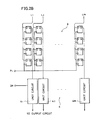
- the analog pixel signals are simultaneously supplied to the corresponding source lines ls of the TFT array 10 through the output circuit 6 respectively.
- the output circuit 6 is a voltage follower which is connected every source line.
- the reference numeral 7 denotes a gate driving circuit.
- the gate driving circuit 7 receives control signals from the timing generating circuit 1. Scanning pulses are sequentially supplied to the gate lines lg.
- the gate lines lg are arranged in positions corresponding to the pixel signals for one line which are supplied from the output circuit 6 to the source lines ls of the TFT array 10 for each horizontal period.
- the digital video signals SVd for one line are sequentially stored in the shift register circuit 2, held by the latch circuit 3 for one horizontal period and then converted into the analog video signals by the conversion circuit 4 so as to be supplied to the source lines ls of the TFT array 10.
- the scanning pulses are sequentially supplied to the gate lines lg.
- the gate lines lg are arranged in the positions corresponding to the video signals for one line which are supplied to the source lines ls of the TFT array 10.
- Each pixel of the TFT array 10 is driven in response to the analog pixel signals corresponding to each pixel data of the video signals SVd so that an image is displayed.
- the TFT array can sufficiently and accurately be driven corresponding to the video signals SVd.
- the comparison data DR is com pared with the data DL so that the pulse width modulation is performed.
- the comparison data DR is synchronized with the clock CLK so as to be sequentially increased by a quantize step width. It is required to repeat the pulse width modulation about 10 times for one horizontal period so as to obtain the stable analog video signals.
- the pulse width modulation is performed between the voltages VA and VB by the data DL of the lower 4 bits. Consequently, the time for one pulse width modulation can be reduced as compared with the pulse width modulation by the pixel data of 8 bits itself.
- the division of the number of the bits is not limited. In other words, the division is determined in consideration of the cycle of the clocks CLK or the like. Briefly, the bits of the pixel data are divided into the upper 4 bits and the lower 4 bits to reduce the number of the bits related to the pulse width modulation.
- the number of the bits of the pixel data is not limited. If the number of the bits is increased, the present invention becomes more effective.
- the digital video signals are used as described above. Unlike the conventional example, there is not performed a processing in which the pixel signals are sampled from the analog video signals. Consequently, even if the number of the pixels for one line is increased, the TFT array can sufficiently and accurately be driver, corresponding to the video signals.
- the pixel data is classified into the data of the upper and lower bits. The adjacent two different DC voltages are selected according to the data of the upper bits. The pulse width modulation between the two different DC voltages are executed according to the data of the lower bits. Consequently, even if the number of the bits of the pixel data is greater, the time for the pulse width modulation is rarely increased. Therefore, the cycle of the clocks may be longer. In other words, even if the number of the bits of the pixel data is increased, the pixel data can be converted into the analog video signals very well by using a cheap clock generator.
Abstract
Description
- The present invention relates to a driving circuit for driving source lines of an active-matrix type liquid crystal display having a thin film transistor matrix array (TFT array).
- Conventionally, there has been proposed a circuit for driving source lines of an active-matrix type liquid crystal display as shown in Fig. 6.
- In Fig. 6, the
reference numeral 21 denotes a timing generating circuit. Thetiming generating circuit 21 receives horizontal and vertical synchronizing signals HD and VD as reference timing signals. The horizontal and vertical synchronizing signals HD and VD are synchronized with analog video signals to be described below. - A
shift register circuit 22 receives sampling clocks CK and start pulses P ST from thetiming generating circuit 21. - Analog video signals SVa are supplied to a
sampling gate circuit 23. Thegate circuit 23 has a plurality of gate portions. The gate portions sample the video signals Sva to obtain pixel signals. In addition, the gate portions receive gate pulses P SG from theshift register circuit 22 to sample the pixel signals for one line for each horizontal period. - A
latch gate circuit 24 receives the pixel signals for one line which are sampled by thegate circuit 23. Latch pulses P LG are supplied from thetiming generating circuit 21 to thegate circuit 24 for a horizontal blanking period. Consequently, the pixel signals for one line supplied from thegate circuit 23 are latched and held for a next horizontal period. - The pixel signals for one line outputted from the
gate circuit 24 are simultaneously supplied to corresponding source lines ℓs of aTFT array 10 through anoutput circuit 25. - Fig. 7 is a diagram showing a specific partial construction of the
gate circuits output circuit 25 corresponding to one pixel signal. In other words, the whole of thegate circuits output circuit 25 consists of the predetermined number of the above constructions. The reference numerals G23 and G24 denote gates. The reference numerals C23 and C24 denote capacitors. The reference numeral A25 denotes a buffer. - Returning to Fig. 6, the
timing generating circuit 21 supplies control signals to agate driving circuit 26. Then, scanning pulses are sequentially supplied to gate lines ℓg. The gate lines ℓg are arranged in positions corresponding to the pixel signals for one line which are supplied to the source lines ℓs of theTFT array 10 through theoutput circuit 25. - According to the driving circuit shown in Fig. 6, the analog video signals SVa are inputted. Therefore, if the number of pixels for one line is increased like the
TFT array 10 having a large screen and high quality of image, a sampling time which is allowed for one pixel signal. becomes shorter. Consequently, the time for charging the capacitor C23 of thegate circuit 23 becomes insufficient so that the video signals SVa cannot be sampled accurately. In other words, theTFT array 10 cannot accurately be driven corresponding to the video signals SVa. Therefore, it is difficult to obtain the good quality of display. - Japanese Unexamined Patent Publication Nos. 63-182695 and 63-186295 have disclosed a circuit for driving the liquid crystal display in response to digital video signals. In the former Publication disclosed is a driving circuit for selecting driving voltages corresponding to inputted multigradation digital video signals to output the same to the liquid crystal display. In the latter Publication disclosed is a driving circuit for receiving data which specifies a display brightness for each pixel of the liquid crystal display on the basis of a value represented by a plurality of bits and then outputting a driving signal having a pulse width corresponding to the data.
- The present invention provides a driving circuit of a liquid crystal display for driving source lines of an active-matrix type liquid crystal display having a thin film transistor matrix array comprising a shift register circuit for sequentially storing digital video signals for one line, each of the digital video signals being comprised of pixel data of a series of predetermined bits, a latch circuit for holding for one horizontal period the digital video signals for one line stored in the shift register circuit, a conversion circuit for classifying each pixel data constituting the digital video signals for one line outputted from the latch circuit into upper and lower bits, selecting adjacent two different DC voltages according to a value designated by the upper bits, performing pulse width modulation between the two different DC voltages according to a value designated by the lower bits and supplying analog video signals to the corresponding source lines of the matrix array, and a comparison data generating circuit for outputting comparison data which has bits by number equal to that of the lower bits and is compared with the lower bits to the conversion circuit.
- Fig. 1 is a block diagram showing one embodiment of the present invention;
- Figs. 2A and B are circuit diagrams showing constructions of a shift register circuit, a latch circuit and a conversion circuit;
- Fig. 3 is a circuit diagram showing the conversion circuit of the embodiment;
- Figs. 4A, B and C are diagrams for explaining an operation of the conversion circuit;
- Fig. 5 is a circuit diagram of a comparison data generator and a pulse width modulator of the embodiment;
- Fig. 6 is a block diagram of a conventional example; and
- Fig. 7 is a circuit diagram of a main portion of the conventional example.
- A driving circuit of a liquid crystal display according to the present invention comprises a timing generating circuit, a gate driving circuit, an output circuit and a power circuit basically. The timing generating circuit outputs signals for judging a timing of signal processing. The gate driving circuit drives gate lines of a thin film transistor matrix array (TFT array) of an active-matrix type liquid crystal display to be driven. The output circuit properly levels analog video signals to be supplied to source lines of the TFT array. The power circuit outputs DC voltages.
- According to the driving circuit, digital video signals for one line are sequentially stored in a shift register circuit, held by a latch circuit for one horizontal period and then converted into the analog video signals by a conversion circuit so as to be supplied to the source lines of the TFT array. Unlike a conventional example, there is not performed a processing in which pixel signals are sampled from the analog video signals. Consequently, even if the number of pixels for one line is increased, the TFT array can sufficiently and accurately be driven corresponding to the video signals.
- An example of an active-matrix type liquid crystal display which can be driven by the driving circuit of the present invention is such that pixel electrodes are formed like a matrix in a liquid crystal cell and thin film transistors are respectively connected to the respective pixel electrodes in order to or not to apply voltages thereto so that a thin film transistor matrix array is formed (for example, Japanese Unexamined Patent Publication No. 59492/1986).
- There will be described one embodiment of the present invention with reference to Fig. 1.
- In Fig. 1, the
reference numeral 1 denotes a timing generating circuit. The timing generatingcircuit 1 receives horizontal and vertical synchronizing signals HD and VD as reference timing signals. The horizontal and vertical synchronizing signals HD and VD are synchronized with digital video signals SVd to be described below. - The
reference numeral 2 denotes a shift register circuit. Theshift register circuit 2 sequentially stores the digital video signals for one line which are comprised of pixel data of a series of predetermined bits. In addition, theshift register circuit 2 receives the digital video signals SVd. The digital video signal SVd is comprised of pixel data Pl to Pm which have 8 bits of D0 to D7 respectively. Theshift register circuit 2 receives clocks CLK from thetiming generating circuit 1 and sequentially stores the digital video signals SVd for one line for each horizontal period (see Fig. 2A). - A
latch circuit 3 receives the pixel data for one line which are stored in theshift register circuit 2 for each horizontal period (see Fig. 2B). Latch pulses PL are supplied from thetiming generating circuit 1 to thelatch circuit 3 for a horizontal blanking period so that the pixel data (Ll to Lm) for one line supplied from theshift register circuit 2 are latched and held for a next horizontal period. - A
conversion circuit 4 receives the pixel data for one line outputted from thelatch circuit 3. - The
conversion circuit 4 classifies each pixel data which forms the digital video signals for one line outputted from thelatch circuit 3 into upper bits and lower bits respectively, and then selects adjacent two different DC voltages according to a value designated by the upper bits and performs pulse width modulation between the two different DC voltages according to a value designated by the lower bits to supply the analog video signals to the corresponding source lines of the matrix array. In other words, theconversion circuit 4 classifies each pixel data of 8 bits into data DH (D7 to D4) of the upper 4 bits and data DL (D3 to D0) of the lower 4 bits respectively. - The data DH of the upper 4 bits selects adjacent two different voltages VA and VB which are supplied to the source lines of the
TFT array 10 among voltages V0 (Vmin), V1, V2, ..., V16 (Vmax). The voltages V0 (Vmin), V1, V2, ..., V16 (Vmax) are provided at equal intervals between maximum and minimum voltages Vmax and Vmin. In this case, if a value designated by the data DH is n (n = 0 to 15), VA = Vn+1 and VB = Vn. - The pulse width modulation is executed between the voltages VA and VB selected according to the date DL of the lower bits as described above. Then, pulse width modulation signals are integrated and outputted.
- The
conversion circuit 4 includesunit circuits circuit 41, apulse width modulator 43, two switchingelements circuit 44. The switchingcircuit 41 selects the DC voltages. Thepulse width modulator 43 compares the lower bits with comparison data DR outputted from a comparisondata generating circuit 5 so as to output signals having different pulse widths corresponding to the result of comparison. Theswitching elements circuit 41 in response to the signals outputted from thepulse width modulator 43. The integratingcircuit 44 outputs the analog pixel signals in response to the signals outputted from theswitching elements - Fig. 3 is a diagram showing a construction of one pixel portion of the
conversion circuit 4. - In Fig. 3, the switching
circuit 41 receives the voltages V0 to V16, selects and outputs the voltages VA and VB according to the data DH of the upper 4 bits (see Fig. 4A). - The voltages VA and VB selected by the switching
circuit 41 are supplied to a drain of an N-channel FET (field effect transistor) 42N and to a source of a P-channel FET 42P respectively. - The
reference numeral 43 denotes a pulse width modulator. Thepulse width modulator 43 receives the data DL of the lower 4 bits and the comparison data DR (DR3 to DR0) of 4 bits from the comparison data generating circuit 5 (see Fig. 1). In other words, the comparisondata generating circuit 5 outputs the comparison data, which comprises bits by number equal to that of the lower bits, to be compared with the lower bits to theconversion circuit 4. - Fig. 5 is a diagram showing a specific construction of the comparison
data generating circuit 5 andpulse width modulator 43. - The comparison
data generating circuit 5 is a 4-bit hexadecimal counter which is formed by connecting D flip-flops 51 to 54 in series. A clock terminal of the D flip-flop 51 receives the clocks CLK from thetiming generating circuit 1. The signals DR0 to DR3 at output terminals Q of the D flip-flops 51 to 54 form the 4-bit comparison data DR. The 4-bit comparison data DR repeats [0000] to [1111] in a cycle for 16 clocks of the clock CLK. - The
pulse width modulator 43 is a 4-bit comparator by which the data DL is compared with the comparison data DR. Thepulse width modulator 43 outputs signals S PWM. If the data DL is less than the comparison data DR, the signal S PWM has a low level "0". If the data DL is greater than the comparison data DR, the signal S PWM has a high level "1". In this case, every time the clock CLK is supplied to thecomparison data generator 5, the comparison data DR is incremented. If the comparison data DR is greater than the data DL, the level of the signal S PWM is changed from the high level "1" to the low level "0". Consequently, a period in which the signal S PWM has the high level "1" corresponds to the data DL in the cycle for 16 clocks of the clock CLK. In other words, thepulse width modulator 43 outputs the signals S PWM which are produced by the pulse width modulation on the data DL. - Returning to Fig. 3, the signals S PWM outputted from the
pulse width modulator 43 are supplied to gates of theFETs FET 42N is conductive. If the signal S PWM has the low level "0", theFET 42P is conductive. Accordingly, since the signal S PWM is produced by the pulse width modulation on the data DL, the signals which are produced by the pulse width modulation on the data DL between the voltages VA and VB are outputted to a node of a source of theFET 42N and a drain of theFET 42P (see Fig. 4B). - The integrating
circuit 44 receives the signals which are produced by the pulse width modulation between the voltages VA and VB. As described above, the voltages VA and VB are selected on the basis of the data DH of the upper 4 bits of the pixel data and the pulse width modulation is performed on the basis of the data DL of the lower 4 bits of the pixel data. Consequently, the signals outputted from the integratingcircuit 44 are converted into the analog pixel signals having levels corresponding to the pixel data of 8 bits (see Fig. 4C). - Returning to Fig. 1, the
conversion circuit 4 outputs analog pixel signals which have levels corresponding to the digital pixel data for one line supplied from thelatch circuit 3. The analog pixel signals are simultaneously supplied to the corresponding source lines ℓs of theTFT array 10 through theoutput circuit 6 respectively. Theoutput circuit 6 is a voltage follower which is connected every source line. - The
reference numeral 7 denotes a gate driving circuit. Thegate driving circuit 7 receives control signals from thetiming generating circuit 1. Scanning pulses are sequentially supplied to the gate lines ℓg. The gate lines ℓg are arranged in positions corresponding to the pixel signals for one line which are supplied from theoutput circuit 6 to the source lines ℓs of theTFT array 10 for each horizontal period. - Thus, the digital video signals SVd for one line are sequentially stored in the
shift register circuit 2, held by thelatch circuit 3 for one horizontal period and then converted into the analog video signals by theconversion circuit 4 so as to be supplied to the source lines ℓs of theTFT array 10. In addition, the scanning pulses are sequentially supplied to the gate lines ℓg. The gate lines ℓg are arranged in the positions corresponding to the video signals for one line which are supplied to the source lines ℓs of theTFT array 10. Each pixel of theTFT array 10 is driven in response to the analog pixel signals corresponding to each pixel data of the video signals SVd so that an image is displayed. - According to the present embodiment, there is not performed a processing in which the pixel signals are sampled from the analog video signals SVa. Consequently, even if the number of the pixels for one line is increased, the TFT array can sufficiently and accurately be driven corresponding to the video signals SVd.
- As described above, the comparison data DR is com pared with the data DL so that the pulse width modulation is performed. The comparison data DR is synchronized with the clock CLK so as to be sequentially increased by a quantize step width. It is required to repeat the pulse width modulation about 10 times for one horizontal period so as to obtain the stable analog video signals.
- According to the present embodiment, the pulse width modulation is performed between the voltages VA and VB by the data DL of the lower 4 bits. Consequently, the time for one pulse width modulation can be reduced as compared with the pulse width modulation by the pixel data of 8 bits itself. For the pulse width modulation by the pixel data of 8 bits itself, the time for 10 pulse width modulations is 10 nsec x 256 steps x 10 times = 25.6 µsec if the cycle of the clocks CLK is 10 nsec. For the present embodiment, the time for 10 pulse width modulations is 10 nsec x 16 steps x 10 times = 1.6 µsec if the cycle of the clocks CLK is 10 nsec. Accordingly, a construction of the present embodiment causes the cycle of the clocks to be longer. In addition, even if a cheap clock generator is used, the pixel data can be converted into the analog video signals very well.
- While the pixel data of 8 bits is classified into the data of the upper 4 bits and the data of the lower 4 bits in the present embodiment, the division of the number of the bits is not limited. In other words, the division is determined in consideration of the cycle of the clocks CLK or the like. Briefly, the bits of the pixel data are divided into the upper 4 bits and the lower 4 bits to reduce the number of the bits related to the pulse width modulation.
- While the pixel data of 8 bits are used in the above present embodiment, the number of the bits of the pixel data is not limited. If the number of the bits is increased, the present invention becomes more effective.
- According to the present invention, the digital video signals are used as described above. Unlike the conventional example, there is not performed a processing in which the pixel signals are sampled from the analog video signals. Consequently, even if the number of the pixels for one line is increased, the TFT array can sufficiently and accurately be driver, corresponding to the video signals. In addition, the pixel data is classified into the data of the upper and lower bits. The adjacent two different DC voltages are selected according to the data of the upper bits. The pulse width modulation between the two different DC voltages are executed according to the data of the lower bits. Consequently, even if the number of the bits of the pixel data is greater, the time for the pulse width modulation is rarely increased. Therefore, the cycle of the clocks may be longer. In other words, even if the number of the bits of the pixel data is increased, the pixel data can be converted into the analog video signals very well by using a cheap clock generator.
- The invention being thus described, it will be obvious that the same may be varied in many ways. Such variations are not to be regarded as a departure from the scope of the invention.
- There are described above novel features which the skilled man will appreciate give rise to advantages. These are each independent aspects of the invention to be covered by the present application, irrespective of whether or not they are included within the scope of the following claims.
Claims (7)
- A driving circuit of a liquid crystal display for driving source lines of an active-matrix type liquid crystal display having a thin film transistor matrix array comprising:a shift register circuit for sequentially storing digital video signals for one line, each of the digital video signals being comprised of pixel data of a series of predetermined bits;a latch circuit for holding for one horizontal period the digital video signals for one line stored in the shift register circuit;a conversion circuit for classifying each pixel data constituting the digital video signals for one line outputted from the latch circuit into upper and lower bits, selecting adjacent two different DC voltages according to a value designated by the upper bits, performing pulse width modulation between the two different DC voltages according to a value designated by the lower bits and supplying analog video signals to the corresponding source lines of the matrix array; anda comparison data generating circuit for outputting comparison data which has bits by number equal to that of the lower bits and is compared with the lower bits to the conversion circuit.
- A driving circuit according to Claim 1 wherein the conversion circuit includes unit circuits by number corresponding to that of the pixel data for one line, the unit circuit having a switching circuit for selecting the two different DC voltages, a pulse width modulator for comparing the lower bits with the comparison data outputted from the comparison data generating circuit and then outputting signals which have different pulse widths corresponding to the result of comparison, two switching elements for respectively switching the two different DC voltages outputted from the switching circuit in response to the signals outputted from the pulse width modulator, and an integrating circuit for outputting analog pixel signals in response to the signals outputted from the respective switching elements.
- A driving circuit according to Claim 1 wherein the comparison data generating circuit is a hexadecimal counter which is formed by connecting four D flip-flops in series.
- A driving circuit according to Claim 2 wherein the pulse width convertor is a 4-bit comparator and the comparison data generating circuit is a hexadecimal counter which is formed by connecting four D flip-flops in series.
- A driving circuit according to Claim 2 wherein the switching elements are N- and P-channel field effect transistors.
- A driving circuit for a multi-element display device, the circuit being operable to provide a plurality of analog output signals for driving respective lines of the display, characterised in that the circuit is responsive to respective digital input signals each of which carries information relating to the magnitude of the output signal to be supplied to a respective line, and in that the driving circuit comprises a plurality of conversion circuits responsive to the respective digital input signals for providing output signals of a desired level.
- A driving circuit for driving respective lines of a matrix display, comprising:storing means for sequentially storing digital signals, each said signal having first and second components;means for holding, for one horizontal period, the signals for one line stored in the storing means;means for selecting first and second voltages in response to said first component of each signal, determining relative durations for said first and second voltages in response to said second component to derive an analog signal, and supplying the analog signal to the corresponding source line of the matrix array.
Applications Claiming Priority (2)
| Application Number | Priority Date | Filing Date | Title |
|---|---|---|---|
| JP324639/89 | 1989-12-14 | ||
| JP1324639A JP2642204B2 (en) | 1989-12-14 | 1989-12-14 | Drive circuit for liquid crystal display |
Publications (3)
| Publication Number | Publication Date |
|---|---|
| EP0433054A2 true EP0433054A2 (en) | 1991-06-19 |
| EP0433054A3 EP0433054A3 (en) | 1992-08-05 |
| EP0433054B1 EP0433054B1 (en) | 1995-07-19 |
Family
ID=18168077
Family Applications (1)
| Application Number | Title | Priority Date | Filing Date |
|---|---|---|---|
| EP90313541A Expired - Lifetime EP0433054B1 (en) | 1989-12-14 | 1990-12-12 | A driving circuit of a liquid crystal display |
Country Status (10)
| Country | Link |
|---|---|
| US (1) | US5162786A (en) |
| EP (1) | EP0433054B1 (en) |
| JP (1) | JP2642204B2 (en) |
| KR (1) | KR940002295B1 (en) |
| CN (1) | CN1021382C (en) |
| AU (1) | AU617258B2 (en) |
| BR (1) | BR9006329A (en) |
| DE (1) | DE69021027T2 (en) |
| ES (1) | ES2074143T3 (en) |
| MY (1) | MY105389A (en) |
Cited By (17)
| Publication number | Priority date | Publication date | Assignee | Title |
|---|---|---|---|---|
| WO1992021122A1 (en) * | 1991-05-15 | 1992-11-26 | International Business Machines Corporation | Liquid crystal display |
| EP0624862A2 (en) * | 1993-05-14 | 1994-11-17 | Sharp Kabushiki Kaisha | Driving circuit for display apparatus |
| EP0655726A1 (en) * | 1993-11-26 | 1995-05-31 | Sharp Kabushiki Kaisha | Grey level selecting circuit for a display driver |
| EP0678846A1 (en) * | 1994-04-04 | 1995-10-25 | Sharp Kabushiki Kaisha | Improvement for power saving in an active matrix display with grey scales |
| EP0712245A3 (en) * | 1994-11-11 | 1997-03-26 | Daewoo Electronics Co Ltd | Actuated mirror array driving circuit having a digital to analog converter |
| US5673061A (en) * | 1993-05-14 | 1997-09-30 | Sharp Kabushiki Kaisha | Driving circuit for display apparatus |
| FR2749431A1 (en) * | 1996-05-31 | 1997-12-05 | Pixtech Sa | Control of brightness of field emission matrix display screen |
| GB2322958A (en) * | 1997-03-05 | 1998-09-09 | Lg Electronics Inc | Source driver for a liquid crystal display |
| US5923312A (en) * | 1994-10-14 | 1999-07-13 | Sharp Kabushiki Kaisha | Driving circuit used in display apparatus and liquid crystal display apparatus using such driving circuit |
| EP1031961A2 (en) | 1999-02-24 | 2000-08-30 | Semiconductor Energy Laboratory Co., Ltd. | Gradation control of a display device |
| EP1037192A2 (en) | 1999-03-18 | 2000-09-20 | Sel Semiconductor Energy Laboratory Co., Ltd. | Gray scale driving for a display device with an active matrix |
| EP1052616A3 (en) * | 1999-05-14 | 2001-07-18 | Sharp Kabushiki Kaisha | Signal line driving circuit and image display device |
| WO2002082417A1 (en) * | 2001-04-06 | 2002-10-17 | Three-Five Systems, Inc. | Liquid crystal display column capacitance charging with a current source |
| WO2004107302A1 (en) * | 2003-05-28 | 2004-12-09 | Koninklijke Philips Electronics N.V. | Active matrix display device |
| US6952194B1 (en) | 1999-03-31 | 2005-10-04 | Semiconductor Energy Laboratory Co., Ltd. | Liquid crystal display device |
| US7145536B1 (en) | 1999-03-26 | 2006-12-05 | Semiconductor Energy Laboratory Co., Ltd. | Liquid crystal display device |
| US7301520B2 (en) | 2000-02-22 | 2007-11-27 | Semiconductor Energy Laboratory Co., Ltd. | Image display device and driver circuit therefor |
Families Citing this family (39)
| Publication number | Priority date | Publication date | Assignee | Title |
|---|---|---|---|---|
| US5416496A (en) * | 1989-08-22 | 1995-05-16 | Wood; Lawson A. | Ferroelectric liquid crystal display apparatus and method |
| JP2724053B2 (en) * | 1991-03-29 | 1998-03-09 | 沖電気工業株式会社 | LCD drive circuit |
| EP0515191B1 (en) * | 1991-05-21 | 1998-08-26 | Sharp Kabushiki Kaisha | A display apparatus, a drive circuit for a display apparatus, and a method of driving a display apparatus |
| JPH05100635A (en) * | 1991-10-07 | 1993-04-23 | Nec Corp | Integrated circuit and method for driving active matrix type liquid crystal display |
| JP3212352B2 (en) * | 1992-04-09 | 2001-09-25 | カシオ計算機株式会社 | Display drive |
| JP3324819B2 (en) * | 1993-03-03 | 2002-09-17 | 三菱電機株式会社 | Semiconductor integrated circuit device |
| JPH06274133A (en) * | 1993-03-24 | 1994-09-30 | Sharp Corp | Driving circuit for display device, and display device |
| US5381252A (en) * | 1993-06-22 | 1995-01-10 | Chunghawa Picture Tubes, Ltd. | Opposed scanning electron beams light source for projection LCD |
| JPH07129122A (en) * | 1993-10-28 | 1995-05-19 | Sharp Corp | Display driving device and data transmitting method thereof |
| JP2759108B2 (en) * | 1993-12-29 | 1998-05-28 | カシオ計算機株式会社 | Liquid crystal display |
| US5479187A (en) * | 1994-02-23 | 1995-12-26 | Chunghwa Picture Tubes, Ltd. | Vertically scanned narrow light beam source for LCD display |
| US5592193A (en) * | 1994-03-10 | 1997-01-07 | Chunghwa Picture Tubes, Ltd. | Backlighting arrangement for LCD display panel |
| JP3059048B2 (en) * | 1994-05-19 | 2000-07-04 | シャープ株式会社 | Liquid crystal display device and driving method thereof |
| JP3275991B2 (en) * | 1994-07-27 | 2002-04-22 | シャープ株式会社 | Active matrix display device and driving method thereof |
| US5739805A (en) * | 1994-12-15 | 1998-04-14 | David Sarnoff Research Center, Inc. | Matrix addressed LCD display having LCD age indication, and autocalibrated amplification driver, and a cascaded column driver with capacitor-DAC operating on split groups of data bits |
| US5677703A (en) * | 1995-01-06 | 1997-10-14 | Texas Instruments Incorporated | Data loading circuit for digital micro-mirror device |
| US6107979A (en) * | 1995-01-17 | 2000-08-22 | Texas Instruments Incorporated | Monolithic programmable format pixel array |
| EP1603109A3 (en) * | 1995-02-01 | 2006-01-04 | Seiko Epson Corporation | Active matrix substrate and liquid crystal display device including it |
| CN1039429C (en) * | 1995-05-08 | 1998-08-05 | 化学工业部北京化工研究院 | Corrosion inhibitor for refrigerating fluid |
| US6281891B1 (en) * | 1995-06-02 | 2001-08-28 | Xerox Corporation | Display with array and multiplexer on substrate and with attached digital-to-analog converter integrated circuit having many outputs |
| JP3713084B2 (en) * | 1995-11-30 | 2005-11-02 | 株式会社日立製作所 | Liquid crystal display controller |
| US6088014A (en) * | 1996-05-11 | 2000-07-11 | Hitachi, Ltd. | Liquid crystal display device |
| CN1037520C (en) * | 1996-04-23 | 1998-02-25 | 北京石油化工学院设计所 | Additive for lubricating oil |
| CN1055112C (en) * | 1997-08-07 | 2000-08-02 | 西安石油学院 | Phosphate oil-base pressure cracked liquid gelatinizer and its preparation |
| KR100396160B1 (en) * | 1997-11-01 | 2003-11-28 | 엘지.필립스 엘시디 주식회사 | Data Driving Circuit for Liquid Crystal Panel |
| CN1098347C (en) * | 2000-04-26 | 2003-01-08 | 青岛立大集团股份有限公司 | Rare-earth additive of lubricating oil and its preparing process |
| KR100367014B1 (en) * | 2000-12-29 | 2003-01-09 | 엘지.필립스 엘시디 주식회사 | Liquid Crystal Display and Driving Method Thereof |
| US6771242B2 (en) * | 2001-06-11 | 2004-08-03 | Lg. Philips Lcd Co., Ltd. | Method and apparatus for driving liquid crystal display |
| KR100769168B1 (en) * | 2001-09-04 | 2007-10-23 | 엘지.필립스 엘시디 주식회사 | Method and Apparatus For Driving Liquid Crystal Display |
| JP4480944B2 (en) * | 2002-03-25 | 2010-06-16 | シャープ株式会社 | Shift register and display device using the same |
| US7173639B2 (en) * | 2002-04-10 | 2007-02-06 | Intel Corporation | Spatial light modulator data refresh without tearing artifacts |
| GB2397710A (en) * | 2003-01-25 | 2004-07-28 | Sharp Kk | A shift register for an LCD driver, comprising reset-dominant RS flip-flops |
| JP4516280B2 (en) * | 2003-03-10 | 2010-08-04 | ルネサスエレクトロニクス株式会社 | Display device drive circuit |
| CN1331107C (en) * | 2003-04-02 | 2007-08-08 | 统宝光电股份有限公司 | Driving circuit of electroluminescence display device |
| JP3991003B2 (en) * | 2003-04-09 | 2007-10-17 | 松下電器産業株式会社 | Display device and source drive circuit |
| WO2004097506A2 (en) * | 2003-04-24 | 2004-11-11 | Displaytech, Inc. | Microdisplay and interface on a single chip |
| CN100405448C (en) * | 2004-08-20 | 2008-07-23 | 友达光电股份有限公司 | Over driving voltage producing method in liquid crystal driving system |
| WO2008086222A2 (en) * | 2007-01-04 | 2008-07-17 | Displaytech, Inc | Digital display |
| TWI447691B (en) * | 2011-11-11 | 2014-08-01 | Au Optronics Corp | Method for triggering source drivers |
Citations (4)
| Publication number | Priority date | Publication date | Assignee | Title |
|---|---|---|---|---|
| JPS60116222A (en) * | 1983-11-28 | 1985-06-22 | Nec Corp | Selector circuit |
| GB2204174A (en) * | 1987-04-23 | 1988-11-02 | Seiko Instr Inc | Electro-optical modulator |
| EP0298255A1 (en) * | 1987-06-04 | 1989-01-11 | Seiko Epson Corporation | Circuit for driving a liquid crystal display panel |
| EP0391654A2 (en) * | 1989-04-04 | 1990-10-10 | Sharp Kabushiki Kaisha | A drive circuit for driving an LCD apparatus |
Family Cites Families (9)
| Publication number | Priority date | Publication date | Assignee | Title |
|---|---|---|---|---|
| JPS54109722A (en) * | 1978-02-16 | 1979-08-28 | Sony Corp | Flat-type picture display device |
| US4590457A (en) * | 1983-12-20 | 1986-05-20 | American Microsystems, Inc. | Digital to analog converter utilizing pulse width modulation |
| JPS6273294A (en) * | 1985-09-27 | 1987-04-03 | カシオ計算機株式会社 | Image display unit |
| KR910001848B1 (en) * | 1986-02-06 | 1991-03-28 | 세이꼬 엡슨 가부시끼가이샤 | Liquid crystal displayy |
| JPS63165860A (en) * | 1986-12-26 | 1988-07-09 | Toshiba Corp | Electrophotographic sensitive body |
| JPH07104662B2 (en) * | 1987-01-23 | 1995-11-13 | ホシデン株式会社 | Liquid crystal display |
| JPS63186295A (en) * | 1987-01-29 | 1988-08-01 | 富士電機株式会社 | Driving circuit for display panel |
| JPH0654421B2 (en) * | 1987-12-07 | 1994-07-20 | シャープ株式会社 | Column electrode driving circuit of matrix type liquid crystal display device |
| DE69020036T2 (en) * | 1989-04-04 | 1996-02-15 | Sharp Kk | Control circuit for a matrix display device with liquid crystals. |
-
1989
- 1989-12-14 JP JP1324639A patent/JP2642204B2/en not_active Expired - Fee Related
-
1990
- 1990-11-28 US US07/619,239 patent/US5162786A/en not_active Expired - Lifetime
- 1990-12-03 AU AU67712/90A patent/AU617258B2/en not_active Expired
- 1990-12-05 KR KR1019900019908A patent/KR940002295B1/en not_active IP Right Cessation
- 1990-12-08 MY MYPI90002152A patent/MY105389A/en unknown
- 1990-12-12 ES ES90313541T patent/ES2074143T3/en not_active Expired - Lifetime
- 1990-12-12 DE DE69021027T patent/DE69021027T2/en not_active Expired - Lifetime
- 1990-12-12 EP EP90313541A patent/EP0433054B1/en not_active Expired - Lifetime
- 1990-12-13 BR BR909006329A patent/BR9006329A/en not_active IP Right Cessation
- 1990-12-14 CN CN90106053A patent/CN1021382C/en not_active Expired - Lifetime
Patent Citations (4)
| Publication number | Priority date | Publication date | Assignee | Title |
|---|---|---|---|---|
| JPS60116222A (en) * | 1983-11-28 | 1985-06-22 | Nec Corp | Selector circuit |
| GB2204174A (en) * | 1987-04-23 | 1988-11-02 | Seiko Instr Inc | Electro-optical modulator |
| EP0298255A1 (en) * | 1987-06-04 | 1989-01-11 | Seiko Epson Corporation | Circuit for driving a liquid crystal display panel |
| EP0391654A2 (en) * | 1989-04-04 | 1990-10-10 | Sharp Kabushiki Kaisha | A drive circuit for driving an LCD apparatus |
Non-Patent Citations (1)
| Title |
|---|
| PATENT ABSTRACTS OF JAPAN vol. 9, no. 270 (E-353)(1993) 26 October 1985 & JP-A-60 116 222 ( NIPPON DENKI K.K. ) 22 June 1985 * |
Cited By (32)
| Publication number | Priority date | Publication date | Assignee | Title |
|---|---|---|---|---|
| US5438342A (en) * | 1991-05-15 | 1995-08-01 | International Business Machines Corporation | Liquid crystal display apparatus and method and apparatus for driving same |
| WO1992021122A1 (en) * | 1991-05-15 | 1992-11-26 | International Business Machines Corporation | Liquid crystal display |
| US5673061A (en) * | 1993-05-14 | 1997-09-30 | Sharp Kabushiki Kaisha | Driving circuit for display apparatus |
| EP0624862A3 (en) * | 1993-05-14 | 1995-05-17 | Sharp Kk | Driving circuit for display apparatus. |
| EP0624862A2 (en) * | 1993-05-14 | 1994-11-17 | Sharp Kabushiki Kaisha | Driving circuit for display apparatus |
| EP0655726A1 (en) * | 1993-11-26 | 1995-05-31 | Sharp Kabushiki Kaisha | Grey level selecting circuit for a display driver |
| EP0678846A1 (en) * | 1994-04-04 | 1995-10-25 | Sharp Kabushiki Kaisha | Improvement for power saving in an active matrix display with grey scales |
| US5614922A (en) * | 1994-04-04 | 1997-03-25 | Sharp Kabushiki Kaisha | Display apparatus |
| US5923312A (en) * | 1994-10-14 | 1999-07-13 | Sharp Kabushiki Kaisha | Driving circuit used in display apparatus and liquid crystal display apparatus using such driving circuit |
| US5793348A (en) * | 1994-11-11 | 1998-08-11 | Daewoo Electronics Co., Ltd. | Actuated mirror array driving circuit having a DAC |
| EP0712245A3 (en) * | 1994-11-11 | 1997-03-26 | Daewoo Electronics Co Ltd | Actuated mirror array driving circuit having a digital to analog converter |
| FR2749431A1 (en) * | 1996-05-31 | 1997-12-05 | Pixtech Sa | Control of brightness of field emission matrix display screen |
| GB2322958A (en) * | 1997-03-05 | 1998-09-09 | Lg Electronics Inc | Source driver for a liquid crystal display |
| GB2322958B (en) * | 1997-03-05 | 2000-07-19 | Lg Electronics Inc | Source driver of liquid crystal display |
| EP1031961A3 (en) * | 1999-02-24 | 2001-10-31 | Semiconductor Energy Laboratory Co., Ltd. | Gradation control of a display device |
| EP1031961A2 (en) | 1999-02-24 | 2000-08-30 | Semiconductor Energy Laboratory Co., Ltd. | Gradation control of a display device |
| US7233342B1 (en) | 1999-02-24 | 2007-06-19 | Semiconductor Energy Laboratory Co., Ltd. | Time and voltage gradation driven display device |
| EP1037192A3 (en) * | 1999-03-18 | 2001-01-17 | Sel Semiconductor Energy Laboratory Co., Ltd. | Gray scale driving for a display device with an active matrix |
| US7714825B2 (en) | 1999-03-18 | 2010-05-11 | Semiconductor Energy Laboratory Co., Ltd. | Display device |
| US8570263B2 (en) | 1999-03-18 | 2013-10-29 | Semiconductor Energy Laboratory Co., Ltd. | Electronic equipment including LED backlight |
| EP1037192A2 (en) | 1999-03-18 | 2000-09-20 | Sel Semiconductor Energy Laboratory Co., Ltd. | Gray scale driving for a display device with an active matrix |
| US7193594B1 (en) | 1999-03-18 | 2007-03-20 | Semiconductor Energy Laboratory Co., Ltd. | Display device |
| US7145536B1 (en) | 1999-03-26 | 2006-12-05 | Semiconductor Energy Laboratory Co., Ltd. | Liquid crystal display device |
| US8144278B2 (en) | 1999-03-26 | 2012-03-27 | Semiconductor Energy Laboratory Co., Ltd. | Optically compensated birefringence mode liquid crystal display device |
| US8896639B2 (en) | 1999-03-26 | 2014-11-25 | Semiconductor Energy Laboratory Co., Ltd. | Liquid crystal display device |
| US9704444B2 (en) | 1999-03-26 | 2017-07-11 | Semiconductor Energy Laboratory Co., Ltd. | Liquid crystal display device |
| US6952194B1 (en) | 1999-03-31 | 2005-10-04 | Semiconductor Energy Laboratory Co., Ltd. | Liquid crystal display device |
| US7042433B1 (en) | 1999-05-14 | 2006-05-09 | Sharp Kabushiki Kaisha | Signal line driving circuit and image display device |
| EP1052616A3 (en) * | 1999-05-14 | 2001-07-18 | Sharp Kabushiki Kaisha | Signal line driving circuit and image display device |
| US7301520B2 (en) | 2000-02-22 | 2007-11-27 | Semiconductor Energy Laboratory Co., Ltd. | Image display device and driver circuit therefor |
| WO2002082417A1 (en) * | 2001-04-06 | 2002-10-17 | Three-Five Systems, Inc. | Liquid crystal display column capacitance charging with a current source |
| WO2004107302A1 (en) * | 2003-05-28 | 2004-12-09 | Koninklijke Philips Electronics N.V. | Active matrix display device |
Also Published As
| Publication number | Publication date |
|---|---|
| KR910013034A (en) | 1991-08-08 |
| MY105389A (en) | 1994-09-30 |
| AU617258B2 (en) | 1991-11-21 |
| CN1052565A (en) | 1991-06-26 |
| JP2642204B2 (en) | 1997-08-20 |
| EP0433054A3 (en) | 1992-08-05 |
| US5162786A (en) | 1992-11-10 |
| BR9006329A (en) | 1991-09-24 |
| AU6771290A (en) | 1991-08-29 |
| EP0433054B1 (en) | 1995-07-19 |
| DE69021027D1 (en) | 1995-08-24 |
| JPH03184018A (en) | 1991-08-12 |
| DE69021027T2 (en) | 1996-01-25 |
| CN1021382C (en) | 1993-06-23 |
| KR940002295B1 (en) | 1994-03-21 |
| ES2074143T3 (en) | 1995-09-01 |
Similar Documents
| Publication | Publication Date | Title |
|---|---|---|
| EP0433054B1 (en) | A driving circuit of a liquid crystal display | |
| US7812807B2 (en) | Display device and driving device | |
| US6624800B2 (en) | Controller circuit for liquid crystal matrix display devices | |
| EP0861484B1 (en) | Lcd driver ic with pixel inversion operation | |
| US6067066A (en) | Voltage output circuit and image display device | |
| US5604511A (en) | Active matrix liquid crystal display apparatus | |
| US5337070A (en) | Display and the method of driving the same | |
| KR100324048B1 (en) | Semiconductor device and liquid crystal display device for driving control of liquid crystal display device | |
| EP0767449B1 (en) | Method and circuit for driving active matrix liquid crystal panel with control of the average driving voltage | |
| EP0508628A2 (en) | Method for driving active matrix type liquid crystal display device | |
| US7277078B2 (en) | Display device | |
| US20080198150A1 (en) | Display device | |
| JP3045266B2 (en) | Drive circuit for liquid crystal display | |
| EP0624862B1 (en) | Driving circuit for display apparatus | |
| US5251051A (en) | Circuit for driving liquid crystal panel | |
| KR100256002B1 (en) | Display device, drive circuit for the display device and method of driving the display device | |
| KR100861270B1 (en) | Liquid crystal display apparatus and mehtod of driving the same | |
| US6518947B1 (en) | LCD column driving apparatus and method | |
| EP0544427A2 (en) | Display module drive circuit having a digital source driver capable of generating multi-level drive voltages from a single external power source | |
| JP3309934B2 (en) | Display device | |
| JPH07181924A (en) | Driving circuit of display device | |
| JPH0446386A (en) | Driving circuit for liquid crystal display device | |
| US20020118156A1 (en) | Liquid crystal device, image processing device, image display apparatus with these devices, signal input method, and image processing method | |
| JPH06230340A (en) | Driving circuit of liquid crystal display device | |
| JP2598474Y2 (en) | Grayscale driving circuit for active matrix type liquid crystal display |
Legal Events
| Date | Code | Title | Description |
|---|---|---|---|
| PUAI | Public reference made under article 153(3) epc to a published international application that has entered the european phase |
Free format text: ORIGINAL CODE: 0009012 |
|
| 17P | Request for examination filed |
Effective date: 19901220 |
|
| AK | Designated contracting states |
Kind code of ref document: A2 Designated state(s): DE ES FR GB |
|
| PUAL | Search report despatched |
Free format text: ORIGINAL CODE: 0009013 |
|
| AK | Designated contracting states |
Kind code of ref document: A3 Designated state(s): DE ES FR GB |
|
| 17Q | First examination report despatched |
Effective date: 19940208 |
|
| GRAA | (expected) grant |
Free format text: ORIGINAL CODE: 0009210 |
|
| AK | Designated contracting states |
Kind code of ref document: B1 Designated state(s): DE ES FR GB |
|
| REF | Corresponds to: |
Ref document number: 69021027 Country of ref document: DE Date of ref document: 19950824 |
|
| ET | Fr: translation filed | ||
| REG | Reference to a national code |
Ref country code: ES Ref legal event code: FG2A Ref document number: 2074143 Country of ref document: ES Kind code of ref document: T3 |
|
| PLBE | No opposition filed within time limit |
Free format text: ORIGINAL CODE: 0009261 |
|
| STAA | Information on the status of an ep patent application or granted ep patent |
Free format text: STATUS: NO OPPOSITION FILED WITHIN TIME LIMIT |
|
| 26N | No opposition filed | ||
| REG | Reference to a national code |
Ref country code: GB Ref legal event code: IF02 |
|
| PGFP | Annual fee paid to national office [announced via postgrant information from national office to epo] |
Ref country code: ES Payment date: 20091229 Year of fee payment: 20 |
|
| PGFP | Annual fee paid to national office [announced via postgrant information from national office to epo] |
Ref country code: GB Payment date: 20091209 Year of fee payment: 20 Ref country code: FR Payment date: 20091221 Year of fee payment: 20 |
|
| PGFP | Annual fee paid to national office [announced via postgrant information from national office to epo] |
Ref country code: DE Payment date: 20091222 Year of fee payment: 20 |
|
| REG | Reference to a national code |
Ref country code: GB Ref legal event code: PE20 Expiry date: 20101211 |
|
| PG25 | Lapsed in a contracting state [announced via postgrant information from national office to epo] |
Ref country code: GB Free format text: LAPSE BECAUSE OF EXPIRATION OF PROTECTION Effective date: 20101211 |
|
| REG | Reference to a national code |
Ref country code: ES Ref legal event code: FD2A Effective date: 20120511 |
|
| PG25 | Lapsed in a contracting state [announced via postgrant information from national office to epo] |
Ref country code: ES Free format text: LAPSE BECAUSE OF EXPIRATION OF PROTECTION Effective date: 20101213 |
|
| PG25 | Lapsed in a contracting state [announced via postgrant information from national office to epo] |
Ref country code: DE Free format text: LAPSE BECAUSE OF EXPIRATION OF PROTECTION Effective date: 20101212 |