EP0439227A1 - Semiconductor device comprising a support, method of manufacturing it, and method of manufacturing the support - Google Patents
Semiconductor device comprising a support, method of manufacturing it, and method of manufacturing the support Download PDFInfo
- Publication number
- EP0439227A1 EP0439227A1 EP91200094A EP91200094A EP0439227A1 EP 0439227 A1 EP0439227 A1 EP 0439227A1 EP 91200094 A EP91200094 A EP 91200094A EP 91200094 A EP91200094 A EP 91200094A EP 0439227 A1 EP0439227 A1 EP 0439227A1
- Authority
- EP
- European Patent Office
- Prior art keywords
- groove
- conductors
- semiconductor
- walls
- support
- Prior art date
- Legal status (The legal status is an assumption and is not a legal conclusion. Google has not performed a legal analysis and makes no representation as to the accuracy of the status listed.)
- Granted
Links
Images

Classifications
-
- H—ELECTRICITY
- H01—ELECTRIC ELEMENTS
- H01L—SEMICONDUCTOR DEVICES NOT COVERED BY CLASS H10
- H01L23/00—Details of semiconductor or other solid state devices
- H01L23/48—Arrangements for conducting electric current to or from the solid state body in operation, e.g. leads, terminal arrangements ; Selection of materials therefor
- H01L23/488—Arrangements for conducting electric current to or from the solid state body in operation, e.g. leads, terminal arrangements ; Selection of materials therefor consisting of soldered or bonded constructions
- H01L23/498—Leads, i.e. metallisations or lead-frames on insulating substrates, e.g. chip carriers
- H01L23/49838—Geometry or layout
- H01L23/49844—Geometry or layout for devices being provided for in H01L29/00
-
- H—ELECTRICITY
- H01—ELECTRIC ELEMENTS
- H01L—SEMICONDUCTOR DEVICES NOT COVERED BY CLASS H10
- H01L23/00—Details of semiconductor or other solid state devices
- H01L23/48—Arrangements for conducting electric current to or from the solid state body in operation, e.g. leads, terminal arrangements ; Selection of materials therefor
-
- H—ELECTRICITY
- H01—ELECTRIC ELEMENTS
- H01L—SEMICONDUCTOR DEVICES NOT COVERED BY CLASS H10
- H01L23/00—Details of semiconductor or other solid state devices
- H01L23/12—Mountings, e.g. non-detachable insulating substrates
- H01L23/13—Mountings, e.g. non-detachable insulating substrates characterised by the shape
-
- H—ELECTRICITY
- H01—ELECTRIC ELEMENTS
- H01L—SEMICONDUCTOR DEVICES NOT COVERED BY CLASS H10
- H01L23/00—Details of semiconductor or other solid state devices
- H01L23/48—Arrangements for conducting electric current to or from the solid state body in operation, e.g. leads, terminal arrangements ; Selection of materials therefor
- H01L23/488—Arrangements for conducting electric current to or from the solid state body in operation, e.g. leads, terminal arrangements ; Selection of materials therefor consisting of soldered or bonded constructions
- H01L23/498—Leads, i.e. metallisations or lead-frames on insulating substrates, e.g. chip carriers
- H01L23/49805—Leads, i.e. metallisations or lead-frames on insulating substrates, e.g. chip carriers the leads being also applied on the sidewalls or the bottom of the substrate, e.g. leadless packages for surface mounting
-
- H—ELECTRICITY
- H01—ELECTRIC ELEMENTS
- H01L—SEMICONDUCTOR DEVICES NOT COVERED BY CLASS H10
- H01L24/00—Arrangements for connecting or disconnecting semiconductor or solid-state bodies; Methods or apparatus related thereto
- H01L24/93—Batch processes
- H01L24/95—Batch processes at chip-level, i.e. with connecting carried out on a plurality of singulated devices, i.e. on diced chips
- H01L24/97—Batch processes at chip-level, i.e. with connecting carried out on a plurality of singulated devices, i.e. on diced chips the devices being connected to a common substrate, e.g. interposer, said common substrate being separable into individual assemblies after connecting
-
- H—ELECTRICITY
- H01—ELECTRIC ELEMENTS
- H01L—SEMICONDUCTOR DEVICES NOT COVERED BY CLASS H10
- H01L2924/00—Indexing scheme for arrangements or methods for connecting or disconnecting semiconductor or solid-state bodies as covered by H01L24/00
- H01L2924/095—Indexing scheme for arrangements or methods for connecting or disconnecting semiconductor or solid-state bodies as covered by H01L24/00 with a principal constituent of the material being a combination of two or more materials provided in the groups H01L2924/013 - H01L2924/0715
- H01L2924/097—Glass-ceramics, e.g. devitrified glass
- H01L2924/09701—Low temperature co-fired ceramic [LTCC]
-
- H—ELECTRICITY
- H01—ELECTRIC ELEMENTS
- H01L—SEMICONDUCTOR DEVICES NOT COVERED BY CLASS H10
- H01L2924/00—Indexing scheme for arrangements or methods for connecting or disconnecting semiconductor or solid-state bodies as covered by H01L24/00
- H01L2924/10—Details of semiconductor or other solid state devices to be connected
- H01L2924/11—Device type
- H01L2924/12—Passive devices, e.g. 2 terminal devices
- H01L2924/1204—Optical Diode
- H01L2924/12042—LASER
-
- H—ELECTRICITY
- H01—ELECTRIC ELEMENTS
- H01L—SEMICONDUCTOR DEVICES NOT COVERED BY CLASS H10
- H01L2924/00—Indexing scheme for arrangements or methods for connecting or disconnecting semiconductor or solid-state bodies as covered by H01L24/00
- H01L2924/10—Details of semiconductor or other solid state devices to be connected
- H01L2924/11—Device type
- H01L2924/14—Integrated circuits
Definitions
- the invention relates to a semiconductor device comprising a support provided with a groove having walls on which conductors are present, which conductors extend to on the support, and with a semiconductor element which is present in the groove and makes electrical contact with the conductors on the walls.
- the invention further relates to a method of manufacturing such a device and to a method of manufacturing a support rod which can be used for the manufacture of the semiconductor device.
- Such a device can be used as a "surface mounting device”.
- the support can be fastened on a PC-board, the conductors present on the support then making electrical contact with conductors on the PC-board.
- British Patent no. 1597707 discloses a device of the kind mentioned in the opening paragraph in which a semiconductor element is mounted in a V-shaped groove.
- the semiconductor element is fastened to a conductor on one of the walls and connected to the conductor on the other wall by means of a connection wire.
- the known device described has the disadvantage that separate process steps are required for fastening the semiconductor element on the support and for providing the connection wire. Since the walls of the groove are oblique and since the semiconductor element in practice has very small dimensions, these process steps are in addition difficult to carry out.
- the invention has for its object inter alia to counteract the disadvantages described.
- the device is characterized in that the semiconductor element is clamped in the groove, thus making electrical contact with the conductors on the walls. Since the semiconductor element is clamped between the conductors on the walls, it is achieved that both a mechanical and an electrical connection is effected between the semiconductor element and the support in a single process step and in a simple manner. Thanks to this simple manner of effecting a connection between the support and the semiconductor element, it is also possible to use very small semiconductor elements in such a semiconductor device.
- the semiconductor elements may be clamped in the groove in that the support is so deformed that the groove is bent open, the semiconductor elements are inserted into the groove, and the support is allowed to spring back. It is also possible to heat the support, the groove becoming larger through expansion, upon which the semiconductor elements can be inserted, after which the semiconductor elements are clamped in through contraction of the groove during cooling-down, and an electrical connection is created.
- the device according to the invention is characterized in that the groove has a tapering shape with a cross-section which becomes smaller in downward direction, in which groove the semiconductor element is automatically held with clamping fit. It is achieved in this way that the semiconductor device can be manufactured by simply pushing the semiconductor element into the groove.
- the semiconductor device is characterized in that the walls of the groove enclose an angle of 5 to 15°. If the walls of the groove enclose an angle smaller than approximately 5°, it appears in practice during the manufacture of the support that the groove occasionally fails to exhibit a tapering shape owing to tolerances on the groove dimensions. The semiconductor element is not satisfactorily clamped in the groove in the case of an angle greater than approximately 15°.
- a more secure connection between semiconductor element and support may be obtained in that one of the conductors or the semiconductor element is provided with a solder layer before the semiconductor element is inserted, in that then the semiconductor element is inserted, upon which the semiconductor device thus created is heated.
- a soldered connection is provided between the semiconductor element and the conductor in this way.
- a deformable contact body is provided between the semiconductor element and one of the conductors in the groove. High mechanical stresses which may occur between the support and the semiconductor element during insertion and during operation of the semiconductor element can be absorbed by this contact body.
- a metal layer provided by electrodeposition or a drop of conducting glue may be used as the deformable contact body.
- the deformable contact body is a bump contact which is provided on the semiconductor element through wire bonding. This means that a wire is bonded to a connection surface of the semiconductor element and then broken off close to the connection surface.
- a bump contact preferably made of gold or silver, can be manufactured in known manner on existing machines and is capable of satisfactorily absorbing the said stresses, as has been demonstrated in practice.
- the invention further relates to a method of manufacturing a device as mentioned in the opening paragraph.
- this method is characterized in that it starts with a support rod provided with a continuous groove having walls on which electrical conductors are present, which conductors extend to on the support rod, upon which semiconductor elements are provided in the groove with clamping fit, after which the support rod is subdivided into a number of semiconductor devices.
- the support rod may be manufactured in a simple manner from a ceramic material by, for example, a sintering process, from a synthetic material by, for example, an injection-moulding process, from a metal covered with an insulating material, such as anodized aluminium, by, for example, an extrusion process, or from a glass by, for example, drawing of a rod.
- a semiconductor element can be fixed and contacted on a support which is suitable for SMD mounting in a simple and inexpensive manner by means of the method.
- the groove is filled with a protective lacquer to protect the semiconductor element from atmospheric influences.
- the semiconductor elements are mounted before the support rod is subdivided.
- the semiconductor elements are provided in the groove with clamping fit by being pushed into a tapering groove with a cross-section which becomes smaller in downward direction, in which groove the semiconductor elements are automatically held with clamping fit.
- the dimensions of the groove are such during this that a semiconductor element achieves a pressure contact in the tapering portion of the groove and thus makes an electrical connection. In this way the semiconductor elements can be fastened and contacted in the groove simply by being pushed into this groove.
- a solder layer is provided on the conductors or on the semiconductor elements before the semiconductor elements are inserted into the groove, while the support rod with semiconductor elements is heated after the semiconductor elements have been inserted. If a temperature above the melting point of the solder layer is achieved during this, the solder layer will flow and a soldered joint will be made. If the temperature remains below the melting point of the solder layer, a thermocompression connection will be made. Such a more secure connection is thus realised in a very simple manner.
- deformable contact bodies are provided on the semiconductor elements before the semiconductor elements are inserted in the groove.
- the contact body can then be provided in a simple manner because the surface of the semiconductor element is readily accessible.
- the contact bodies are provided on the semiconductor elements while the latter are still on a semiconductor slice, after which the slice is divided into individual semiconductor elements which are inserted in the groove.
- a contact body can be provided on each semiconductor element in a simple manner by means of usual machines, since the semiconductor elements assume fixed, well-defined positions on the slice.
- the walls of the groove of the support rod can be provided with conductors in a certain pattern, so that also semiconductor elements having more than two contacts, such as, for example, transistors and ICs, can be connected through the provision of several conductors on one wall.
- the conductors may be provided on the support rod in a simple manner in the following sequence:
- Fig. 1 shows a first embodiment of a semiconductor device according to the invention.
- This device as well as the devices yet to be described below are typically suitable for surface mounting; they are often designated “surface mounting device” or SMD.
- Fig. 1 shows a semiconductor device comprising a support 1 provided with a continuous groove 2 having walls 3 and 4, on which walls metal conductors 6 and 7 are present, which conductors extend to on the support, and comprising a semiconductor element which is inside the groove and makes electrical contact with the conductors on the walls.
- the walls 3 and 4 of the groove enclose an angle of approximately 10°.
- the conductors 6 and 7 run from the groove 2 over an upper surface 5 to a side surface 8 of the support, and possibly further to a lower surface 10.
- the conductors 6 and 7 can make electrical contact with conductors on a PC-board.
- a semiconductor element 11 is provided in the groove 2, in the embodiment shown a semiconductor diode. The semiconductor element is clamped in the groove 2, thereby making electrical contact with conductors 6 and 7 on the walls 3 and 4. A mechanical as well as an electrical contact has thus been effected. It is not necessary, accordingly, to include separate process steps for making mechanical and electrical contact in a production process for the device according to the invention.
- the groove 2 is filled with a protective lacquer 13, for example an epoxy resin applied in the liquid state, after the semiconductor element 11 has been inserted. It is also possible to provide a glass over the semiconductor element as an alternative to the protective lacquer.
- the support 1 is formed from a ceramic material, a synthetic material, a metal covered with an insulating material, or a glass.
- the semiconductor element 11 can be automatically provided with clamping fit in that the element is pushed into the groove 2.
- the groove 2 has a tapering shape with a cross-section which becomes smaller in downward direction, so that the semiconductor element can be automatically provided and inserted with clamping fit.
- Fig. 2 shows a cross-section of the support 1.
- the walls 3 and 4 of the groove 2 preferably enclose an angle 15 of 5 to 15°. If the angle 15 is smaller than approximately 5°, it is found in practice during manufacture of the support that the groove ocasionally fails to have a tapering shape owing to tolerances on the groove dimensions. In the case of an angle greater than approximately 15°, the semiconductor element cannot be securely clamped in the groove.
- FIG. 1 shows an embodiment in which walls 3 and 4 enclose an angle of approximately 10°, while both walls enclose an angle of approximately 95° with the upper surface 5.
- Fig. 3 shows an alternative embodiment in which wall 3 is substantially perpendicular to the upper surface and wall 4 encloses an angle of approximately 100° with the upper surface 5.
- a more secure connection between semiconductor element 11 and support 1 may be obtained in that the conductors 6 and 7 and the semiconductor element 11 are provided with solder layers 66, 77 and 116, respectively, (see Fig. 2) of, for example, a usual lead-tin alloy before the semiconductor element 11 is inserted, in that then the semiconductor element is inserted, and the semiconductor device thus created is heated.
- a soldered connection is provided between the semiconductor element and the conductor in this way. It should be noted that the solder layer is indeed drawn on the conductors 6 and 7 and on the semiconductor element 11, but that a more secure connection is also obtained already if this solder layer should be present on only one of the conductors or on the semiconductor element only.
- a deformable contact body 12 is used between the semiconductor element and one of the conductors in the groove in order to prevent high mechanical stresses occurring during positioning of the semiconductor element and during operation.
- a contact body is a bump contact provided on the semiconductor element through wire bonding, i.e. a wire is bonded to a connection surface of the semiconductor element and subsequently broken off close to the connection surface.
- Such a bump contact preferably made of gold or silver, may be manufactured in known manner on existing machines and is capable of absorbing the said stresses satisfactorily, as has been shown in practice.
- the semiconductor device may be connected to a PC-board with its lower side 10 as well as with its upper side 5.
- the groove is provided in a continuous recess 14 in the support (see Figs. 1 and 2).
- Such a recess may be used to hold a drop of glue (not drawn).
- the semiconductor device may then be fixed to a PC-board with its upper side 5 by means of this drop of glue before the semiconductor device is fixed by soldering.
- the recess 14 ensures that the upper surface 5 of the semiconductor device merges well with a surface of the PC-board in spite of the drop of glue, so that a proper soldered joint between conductors present on the upper surface 5 and the side surfaces 8 of the semiconductor device and on the PC-board can be made.
- Fig. 1 shows a semiconductor device comprising a diode.
- the support may also be used, for example, for a transistor or IC, as shown in Fig. 4.
- the contact at a rear side of the semiconductor element may then be the collector contact which is in connection with conductor 6.
- two bump contacts 112 and 212 made of gold may then be present, being the base contact and the emitter contact, which will be in connection with two mutually separated conductors 17 and 27.
- the dimensions of the semiconductor devices manufactured by means of the invention can be very small; for example, the dimensions of the supports for diodes and transistors are 2 mm x 1,25 mm x 1,2 mm (known as 0805 in SMD technology) or 1,5 mm x 0,75 mm x 0,8 mm (known as 0603).
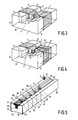
- Fig. 5 shows a step in the production process.
- the process starts with a support rod 51 provided with a continuous groove 52 having walls 53 and 54 on which electrical conductors 56 and 57 are present, which conductors extend to on the support rod 51.
- the support rod is provided with a continuous recess 64.
- the support rod may be made of a ceramic material, such as, for example, silicon carbide, silicon nitride, or aluminium oxide.
- Such a support rod is manufactured, for example, in a sintering process.
- a support rod made of a thermoplastic synthetic material is obtained in known manner, for example, through injection moulding or extrusion. Its shape must then be adapted to the technology used, for example, extrusion.
- the support rod 51 is constructed as a regular body, the continuous groove 2 and the continuous recess 64 run in the extrusion direction. Synthetic materials suitable for this are, for example, polyether sulfon (PES) or polyether imide (PEI). The so-called liquid crystal polymers are also suitable.
- the support rod may also consist of a glass. Such a support rod may be obtained, for example, by drawing or by other methods known in glass technology.
- a number of semiconductor elements 11 can be provided in the groove 52. These semiconductor elements are inserted next to one another in the groove with clamping fit. The elements 11 thereby come into pressure contact with the conductors 56 and 57 on the walls 53 and 54 of the support rod 51.
- the semiconductor elements are covered with a protective lacquer 63, drawn in part in Fig. 5, after which the support rod 51 is subdivided into several semiconductor devices along the broken lines 65 by, for example, sawing or breaking. It is possible thereby to make semiconductor devices consisting of a support provided with one semiconductor element, but also semiconductor devices consisting of a support provided with several semiconductor elements. In the latter semiconductor devices, the conductors 56 and 57 are usually subdivided into several conductor tracks which connect the individual semiconductor elements.
- the semiconductor elements may be provided in various ways.
- the semiconductor element will be included under tension in the groove and an electrical connection will be formed in that the support rod 51 is so deformed that the groove 52 is bent slightly open, upon which the semiconductor elements 11 are inserted and the support body is allowed to spring back.
- the support rod is provided with a tapering groove whose cross-section decreases in downward direction and in which the semiconductor elements can be automatically provided with clamping fit (see Figs. 2 and 5).
- a solder layer of a usual lead-tin alloy is provided on the conductors 56, 57 and on the semiconductor elements 11 before the semiconductor elements are inserted in the groove, which solder layer is not drawn in Fig. 5 for reasons of clarity (these solder layers are identical to the solder layers 66, 67 and 116 indicated in Fig. 2).
- the support rod comprising semiconductor elements is heated. If a temperature above the melting point of the solder layer is reached during this, the solder layer will flow and a soldered joint will be made. If the temperature remains below the melting point of the solder layer, a thermocompression connection will be made. A more secure connection as described is thus realised in a very simple manner.
- a deformable contact body 12 is provided on the semiconductor element 11 before the semiconductor elements are provided in the groove 2.
- the deformable contact body is capable of absorbing the high stresses which occur during insertion of the semiconductor element and during operation of the semiconductor device.
- the contact bodies 12 are preferably provided on the semiconductor elements 11 while these semiconductor elements are still on a semiconductor slice. This can be done, for example, by electrochemically providing a metal layer, thickening the latter and etching it into a pattern, or by providing a drop of conducting glue.
- a bump contact is provided through wire bonding with a conventional wire bonding machine, a small wire being bonded to a connection surface of the semiconductor elements, which wire is subsequently broken off close to the connection surface.
- the semiconductor slice is then subdivided into separate semiconductor elements 11, each provided with a bump contact 12, by means of conventional techniques such as, for example, sawing.
- the invention also relates to a method of manufacturing a support rod 51 which is suitable for accommodating semiconductor elements 11 and which is provided with a continuous groove 52 having walls 53 and 54 on which conductors 56 and 57 are present, which conductors extend to on the support rod 51.
- the conductors according to the invention are provided on the support rod in the following sequence:
Abstract
Description
- The invention relates to a semiconductor device comprising a support provided with a groove having walls on which conductors are present, which conductors extend to on the support, and with a semiconductor element which is present in the groove and makes electrical contact with the conductors on the walls. The invention further relates to a method of manufacturing such a device and to a method of manufacturing a support rod which can be used for the manufacture of the semiconductor device.
- Such a device can be used as a "surface mounting device". The support can be fastened on a PC-board, the conductors present on the support then making electrical contact with conductors on the PC-board.
- British Patent no. 1597707 discloses a device of the kind mentioned in the opening paragraph in which a semiconductor element is mounted in a V-shaped groove. The semiconductor element is fastened to a conductor on one of the walls and connected to the conductor on the other wall by means of a connection wire.
- The known device described has the disadvantage that separate process steps are required for fastening the semiconductor element on the support and for providing the connection wire. Since the walls of the groove are oblique and since the semiconductor element in practice has very small dimensions, these process steps are in addition difficult to carry out.
- The invention has for its object inter alia to counteract the disadvantages described.
- According to the invention, therefore, the device is characterized in that the semiconductor element is clamped in the groove, thus making electrical contact with the conductors on the walls. Since the semiconductor element is clamped between the conductors on the walls, it is achieved that both a mechanical and an electrical connection is effected between the semiconductor element and the support in a single process step and in a simple manner. Thanks to this simple manner of effecting a connection between the support and the semiconductor element, it is also possible to use very small semiconductor elements in such a semiconductor device.
- The semiconductor elements may be clamped in the groove in that the support is so deformed that the groove is bent open, the semiconductor elements are inserted into the groove, and the support is allowed to spring back. It is also possible to heat the support, the groove becoming larger through expansion, upon which the semiconductor elements can be inserted, after which the semiconductor elements are clamped in through contraction of the groove during cooling-down, and an electrical connection is created. Preferably, the device according to the invention is characterized in that the groove has a tapering shape with a cross-section which becomes smaller in downward direction, in which groove the semiconductor element is automatically held with clamping fit. It is achieved in this way that the semiconductor device can be manufactured by simply pushing the semiconductor element into the groove.
- Preferably, the semiconductor device is characterized in that the walls of the groove enclose an angle of 5 to 15°. If the walls of the groove enclose an angle smaller than approximately 5°, it appears in practice during the manufacture of the support that the groove occasionally fails to exhibit a tapering shape owing to tolerances on the groove dimensions. The semiconductor element is not satisfactorily clamped in the groove in the case of an angle greater than approximately 15°.
- A more secure connection between semiconductor element and support may be obtained in that one of the conductors or the semiconductor element is provided with a solder layer before the semiconductor element is inserted, in that then the semiconductor element is inserted, upon which the semiconductor device thus created is heated. A soldered connection is provided between the semiconductor element and the conductor in this way.
- Preferably, a deformable contact body is provided between the semiconductor element and one of the conductors in the groove. High mechanical stresses which may occur between the support and the semiconductor element during insertion and during operation of the semiconductor element can be absorbed by this contact body.
- A metal layer provided by electrodeposition or a drop of conducting glue may be used as the deformable contact body. Preferably, however, the deformable contact body is a bump contact which is provided on the semiconductor element through wire bonding. This means that a wire is bonded to a connection surface of the semiconductor element and then broken off close to the connection surface. Such a bump contact, preferably made of gold or silver, can be manufactured in known manner on existing machines and is capable of satisfactorily absorbing the said stresses, as has been demonstrated in practice.
- The invention further relates to a method of manufacturing a device as mentioned in the opening paragraph. According to the invention, this method is characterized in that it starts with a support rod provided with a continuous groove having walls on which electrical conductors are present, which conductors extend to on the support rod, upon which semiconductor elements are provided in the groove with clamping fit, after which the support rod is subdivided into a number of semiconductor devices. The support rod may be manufactured in a simple manner from a ceramic material by, for example, a sintering process, from a synthetic material by, for example, an injection-moulding process, from a metal covered with an insulating material, such as anodized aluminium, by, for example, an extrusion process, or from a glass by, for example, drawing of a rod. A semiconductor element can be fixed and contacted on a support which is suitable for SMD mounting in a simple and inexpensive manner by means of the method. Preferably, the groove is filled with a protective lacquer to protect the semiconductor element from atmospheric influences.
The semiconductor elements are mounted before the support rod is subdivided. This has the advantage that not every individual support, but only the support rod need be positioned and fixed in machines suitable for that purpose during fastening of the semiconductor elements.
Preferably, the semiconductor elements are provided in the groove with clamping fit by being pushed into a tapering groove with a cross-section which becomes smaller in downward direction, in which groove the semiconductor elements are automatically held with clamping fit. The dimensions of the groove are such during this that a semiconductor element achieves a pressure contact in the tapering portion of the groove and thus makes an electrical connection. In this way the semiconductor elements can be fastened and contacted in the groove simply by being pushed into this groove. - Preferably, a solder layer is provided on the conductors or on the semiconductor elements before the semiconductor elements are inserted into the groove, while the support rod with semiconductor elements is heated after the semiconductor elements have been inserted. If a temperature above the melting point of the solder layer is achieved during this, the solder layer will flow and a soldered joint will be made. If the temperature remains below the melting point of the solder layer, a thermocompression connection will be made. Such a more secure connection is thus realised in a very simple manner.
- Preferably, deformable contact bodies are provided on the semiconductor elements before the semiconductor elements are inserted in the groove. The contact body can then be provided in a simple manner because the surface of the semiconductor element is readily accessible.
- Preferably, the contact bodies are provided on the semiconductor elements while the latter are still on a semiconductor slice, after which the slice is divided into individual semiconductor elements which are inserted in the groove. when the semiconductor elements are still on the slice, a contact body can be provided on each semiconductor element in a simple manner by means of usual machines, since the semiconductor elements assume fixed, well-defined positions on the slice.
- The walls of the groove of the support rod can be provided with conductors in a certain pattern, so that also semiconductor elements having more than two contacts, such as, for example, transistors and ICs, can be connected through the provision of several conductors on one wall. The conductors may be provided on the support rod in a simple manner in the following sequence:
- electroless nucleating of the support rod with a metal,
- local removal of this metal or rendering it insulating,
- electrochemical thickening of the remaining metal.
- The invention will be explained in more detail below with reference to a drawing, by way of example. In the drawing:
- Fig. 1 shows a semiconductor device according to the invention,
- Fig. 2 shows a cross-section of the device of Fig. 1,
- Fig. 3 shows an alternative embodiment of the semiconductor device of Fig. 1,
- Fig. 4 shows the semiconductor device of Fig. 3 comprising a transistor as the semiconductor element,
- Fig. 5 diagrammatically shows a step of the manufacturing process of the device according to Fig. 1.
- The Figures are purely diagrammatical and not drawn to scale. Corresponding parts are indicated with the same reference numerals in the Figures.
- Fig. 1 shows a first embodiment of a semiconductor device according to the invention. This device as well as the devices yet to be described below are typically suitable for surface mounting; they are often designated "surface mounting device" or SMD. Fig. 1 shows a semiconductor device comprising a support 1 provided with a
continuous groove 2 havingwalls 3 and 4, on whichwalls metal conductors walls 3 and 4 of the groove enclose an angle of approximately 10°. Theconductors groove 2 over anupper surface 5 to aside surface 8 of the support, and possibly further to alower surface 10. Theconductors semiconductor element 11 is provided in thegroove 2, in the embodiment shown a semiconductor diode. The semiconductor element is clamped in thegroove 2, thereby making electrical contact withconductors walls 3 and 4. A mechanical as well as an electrical contact has thus been effected. It is not necessary, accordingly, to include separate process steps for making mechanical and electrical contact in a production process for the device according to the invention. Preferably, thegroove 2 is filled with aprotective lacquer 13, for example an epoxy resin applied in the liquid state, after thesemiconductor element 11 has been inserted. It is also possible to provide a glass over the semiconductor element as an alternative to the protective lacquer. - The support 1 is formed from a ceramic material, a synthetic material, a metal covered with an insulating material, or a glass.
- The
semiconductor element 11 can be automatically provided with clamping fit in that the element is pushed into thegroove 2. According to the invention, thegroove 2 has a tapering shape with a cross-section which becomes smaller in downward direction, so that the semiconductor element can be automatically provided and inserted with clamping fit. Fig. 2 shows a cross-section of the support 1. Thewalls 3 and 4 of thegroove 2 preferably enclose an angle 15 of 5 to 15°.
If the angle 15 is smaller than approximately 5°, it is found in practice during manufacture of the support that the groove ocasionally fails to have a tapering shape owing to tolerances on the groove dimensions. In the case of an angle greater than approximately 15°, the semiconductor element cannot be securely clamped in the groove. Fig. 1 shows an embodiment in whichwalls 3 and 4 enclose an angle of approximately 10°, while both walls enclose an angle of approximately 95° with theupper surface 5. Fig. 3 shows an alternative embodiment in whichwall 3 is substantially perpendicular to the upper surface and wall 4 encloses an angle of approximately 100° with theupper surface 5. - A more secure connection between
semiconductor element 11 and support 1 may be obtained in that theconductors semiconductor element 11 are provided withsolder layers semiconductor element 11 is inserted, in that then the semiconductor element is inserted, and the semiconductor device thus created is heated. A soldered connection is provided between the semiconductor element and the conductor in this way. It should be noted that the solder layer is indeed drawn on theconductors semiconductor element 11, but that a more secure connection is also obtained already if this solder layer should be present on only one of the conductors or on the semiconductor element only. - A
deformable contact body 12 is used between the semiconductor element and one of the conductors in the groove in order to prevent high mechanical stresses occurring during positioning of the semiconductor element and during operation. Preferably, such a contact body is a bump contact provided on the semiconductor element through wire bonding, i.e. a wire is bonded to a connection surface of the semiconductor element and subsequently broken off close to the connection surface. Such a bump contact, preferably made of gold or silver, may be manufactured in known manner on existing machines and is capable of absorbing the said stresses satisfactorily, as has been shown in practice. - The semiconductor device may be connected to a PC-board with its
lower side 10 as well as with itsupper side 5. Preferably, the groove is provided in acontinuous recess 14 in the support (see Figs. 1 and 2). Such a recess may be used to hold a drop of glue (not drawn). The semiconductor device may then be fixed to a PC-board with itsupper side 5 by means of this drop of glue before the semiconductor device is fixed by soldering. Therecess 14 ensures that theupper surface 5 of the semiconductor device merges well with a surface of the PC-board in spite of the drop of glue, so that a proper soldered joint between conductors present on theupper surface 5 and the side surfaces 8 of the semiconductor device and on the PC-board can be made. - Fig. 1 shows a semiconductor device comprising a diode. The support may also be used, for example, for a transistor or IC, as shown in Fig. 4. The contact at a rear side of the semiconductor element may then be the collector contact which is in connection with
conductor 6. At a front side of the semiconductor element, for example, twobump contacts conductors - The dimensions of the semiconductor devices manufactured by means of the invention can be very small; for example, the dimensions of the supports for diodes and transistors are 2 mm x 1,25 mm x 1,2 mm (known as 0805 in SMD technology) or 1,5 mm x 0,75 mm x 0,8 mm (known as 0603).
- The semiconductor device described can be manufactured in a simple and inexpensive manner. Fig. 5 shows a step in the production process. The process starts with a
support rod 51 provided with acontinuous groove 52 havingwalls electrical conductors support rod 51. The support rod is provided with acontinuous recess 64. The support rod may be made of a ceramic material, such as, for example, silicon carbide, silicon nitride, or aluminium oxide. Such a support rod is manufactured, for example, in a sintering process. A support rod made of a thermoplastic synthetic material is obtained in known manner, for example, through injection moulding or extrusion. Its shape must then be adapted to the technology used, for example, extrusion. This is the case in the embodiment shown in Fig. 5; thesupport rod 51 is constructed as a regular body, thecontinuous groove 2 and thecontinuous recess 64 run in the extrusion direction. Synthetic materials suitable for this are, for example, polyether sulfon (PES) or polyether imide (PEI). The so-called liquid crystal polymers are also suitable. The support rod may also consist of a glass. Such a support rod may be obtained, for example, by drawing or by other methods known in glass technology. A number ofsemiconductor elements 11 can be provided in thegroove 52. These semiconductor elements are inserted next to one another in the groove with clamping fit. Theelements 11 thereby come into pressure contact with theconductors walls support rod 51. The semiconductor elements are covered with aprotective lacquer 63, drawn in part in Fig. 5, after which thesupport rod 51 is subdivided into several semiconductor devices along thebroken lines 65 by, for example, sawing or breaking. It is possible thereby to make semiconductor devices consisting of a support provided with one semiconductor element, but also semiconductor devices consisting of a support provided with several semiconductor elements. In the latter semiconductor devices, theconductors - The semiconductor elements may be provided in various ways. The semiconductor element will be included under tension in the groove and an electrical connection will be formed in that the
support rod 51 is so deformed that thegroove 52 is bent slightly open, upon which thesemiconductor elements 11 are inserted and the support body is allowed to spring back. It is alternatively possible to heat thesupport rod 51, for example to approximately 250° C, so that it expands, after which the semiconductor elements are provided, so that they will be clamped in the groove after cooling-down. Preferably, the support rod is provided with a tapering groove whose cross-section decreases in downward direction and in which the semiconductor elements can be automatically provided with clamping fit (see Figs. 2 and 5). - Preferably, a solder layer of a usual lead-tin alloy is provided on the
conductors semiconductor elements 11 before the semiconductor elements are inserted in the groove, which solder layer is not drawn in Fig. 5 for reasons of clarity (these solder layers are identical to the solder layers 66, 67 and 116 indicated in Fig. 2). After the semiconductor elements have been provided, the support rod comprising semiconductor elements is heated. If a temperature above the melting point of the solder layer is reached during this, the solder layer will flow and a soldered joint will be made. If the temperature remains below the melting point of the solder layer, a thermocompression connection will be made. A more secure connection as described is thus realised in a very simple manner. - Preferably, a
deformable contact body 12 is provided on thesemiconductor element 11 before the semiconductor elements are provided in thegroove 2. The deformable contact body is capable of absorbing the high stresses which occur during insertion of the semiconductor element and during operation of the semiconductor device. Thecontact bodies 12 are preferably provided on thesemiconductor elements 11 while these semiconductor elements are still on a semiconductor slice. This can be done, for example, by electrochemically providing a metal layer, thickening the latter and etching it into a pattern, or by providing a drop of conducting glue. In the present example a bump contact is provided through wire bonding with a conventional wire bonding machine, a small wire being bonded to a connection surface of the semiconductor elements, which wire is subsequently broken off close to the connection surface. The semiconductor slice is then subdivided intoseparate semiconductor elements 11, each provided with abump contact 12, by means of conventional techniques such as, for example, sawing. - The invention also relates to a method of manufacturing a
support rod 51 which is suitable for accommodatingsemiconductor elements 11 and which is provided with acontinuous groove 52 havingwalls conductors support rod 51. The conductors according to the invention are provided on the support rod in the following sequence: - electroless nucleating of the support rod with a metal, for example electroless nucleating of a support rod obtained through sintering or injection moulding with a metal, such as, for example, nickel, palladium, or silver with a thickness of approximately 0,1 µm,
- local removal of this metal or rendering it insulating throughout its thickness, for example through a treatment with a laser or with UV radiation, whereby the conductor pattern is formed,
- electrochemical thickening of the remaining metal, for example through the application of nickel, silver or copper having a thickness of, for example, 10 µm. If so desired, a standard lead-tin layer which facilitates soldering may be applied over this.
- It will be clear that the embodiments represented in the Figures are merely meant to illustrate examples and that variations are possible within the scope of the invention.
Alternatively, the metal may also be locally provided by means of a laser and electrochemically thickened.
As an alternative to nucleating the support rod with a metal and to local removal or rendering this metal insulating, the support rod may also be locally nucleated in a suitable solution of the metal by means of a laser in known manner.
If the
Claims (14)
- A semiconductor device comprising a support provided with a groove having walls on which conductors are present, which conductors extend to on the support, and with a semiconductor element which is present in the groove and makes electrical contact with the conductors on the walls, characterized in that the semiconductor element is clamped in the groove, thus making electrical contact with the conductors on the walls.
- A semiconductor device as claimed in Claim 1, characterized in that the groove has a tapering shape with a cross-section which becomes smaller in downward direction, in which groove the semiconductor element is automatically held with clamping fit.
- A semiconductor device as claimed in Claim 2, characterized in that the walls of the groove enclose an angle of 5 to 15°.
- A semiconductor device as claimed in any one of the preceding Claims, characterized in that a soldered connection is provided between the semiconductor element and one of the conductors.
- A semiconductor device as claimed in any one of the preceding Claims, characterized in that a deformable contact body is provided between the semiconductor element and one of the conductors.
- A semiconductor device as claimed in Claim 5, characterized in that the deformable contact body is a bump contact provided on the semiconductor element by means of wire bonding.
- A semiconductor device as claimed in Claim 6, characterized in that the bump contact is made of gold or silver.
- A method of manufacturing a semiconductor device comprising a support provided with a groove having walls on which conductors are present, which conductors extend to on the support, and with a semiconductor element which is present in the groove and makes electrical contact with the conductors on the walls, characterized in that it starts with a support rod provided with a continuous groove having walls on which electrical conductors are present, which conductors extend to on the support rod, after which semiconductor elements are provided in the groove with clamping fit, upon which the support rod is subdivided into a number of semiconductor devices.
- A method as claimed in Claim 8, characterized in that the semiconductor elements are provided in the groove with clamping fit by being pushed into a tapering groove with a cross-section which becomes smaller in downward direction, in which groove the semiconductor elements are automatically held with clamping fit.
- A method as claimed in any one of the Claims 8 and 9, characterized in that a solder layer is provided on the conductors or on the semiconductor elements before the semiconductor elements are inserted into the groove, while the support rod with semiconductor elements is heated after the semiconductor elements have been inserted.
- A method as claimed in any one of the Claims 8, 9 or 10, characterized in that deformable contact bodies are provided on the semiconductor elements before the semiconductor elements are inserted in the groove.
- A method as claimed in Claim 11, characterized in that the contact bodies are provided on the semiconductor elements while the latter are still on a semiconductor slice, after which the slice is divided into individual semiconductor elements which are inserted in the groove.
- A method of manufacturing a support rod provided with a groove having walls on which conductors are present, which conductors extend to on the support rod, characterized in that the conductors are provided on the support rod in the following sequence:- electroless nucleating of the support rod with a metal,- local removal of this metal or rendering it insulating,- electrochemical thickening of the remaining metal.
- A method as claimed in Claim 13, characterized in that the metal is locally removed throughout its thickness or rendered insulating by means of a laser or by means of UV radiation.
Applications Claiming Priority (2)
| Application Number | Priority Date | Filing Date | Title |
|---|---|---|---|
| NL9000161 | 1990-01-23 | ||
| NL9000161A NL9000161A (en) | 1990-01-23 | 1990-01-23 | SEMICONDUCTOR DEVICE CONTAINING A CARRIER AND METHOD FOR MANUFACTURING THE CARRIER. |
Publications (2)
| Publication Number | Publication Date |
|---|---|
| EP0439227A1 true EP0439227A1 (en) | 1991-07-31 |
| EP0439227B1 EP0439227B1 (en) | 1997-10-15 |
Family
ID=19856464
Family Applications (1)
| Application Number | Title | Priority Date | Filing Date |
|---|---|---|---|
| EP91200094A Expired - Lifetime EP0439227B1 (en) | 1990-01-23 | 1991-01-21 | Semiconductor device comprising a support, method of manufacturing it, and method of manufacturing the support |
Country Status (7)
| Country | Link |
|---|---|
| US (1) | US5198886A (en) |
| EP (1) | EP0439227B1 (en) |
| JP (1) | JP3040501B2 (en) |
| KR (1) | KR100198209B1 (en) |
| CN (1) | CN1024731C (en) |
| DE (1) | DE69127910T2 (en) |
| NL (1) | NL9000161A (en) |
Cited By (10)
| Publication number | Priority date | Publication date | Assignee | Title |
|---|---|---|---|---|
| WO1995028735A2 (en) * | 1994-04-15 | 1995-10-26 | Philips Electronics N.V. | Method of manufacturing a device whereby a support bar is provided with conductor tracks for electrically contacting a semiconductor element |
| WO1996036075A2 (en) * | 1995-05-10 | 1996-11-14 | Philips Electronics N.V. | Miniature semiconductor device for surface mounting |
| EP0803949A2 (en) * | 1996-04-23 | 1997-10-29 | Compagnie Industrielle Des Lasers Cilas | Laser diode device mounted on semiconducting bars |
| EP1023748A1 (en) * | 1997-10-14 | 2000-08-02 | Decade Products, Inc. | Laser diode assembly |
| WO2005027233A2 (en) * | 2003-09-09 | 2005-03-24 | Cree, Inc. | Solid metal block mounting substrates for semiconductor light emitting devices, and oxidizing methods for fabricating same |
| WO2006114745A2 (en) * | 2005-04-28 | 2006-11-02 | Koninklijke Philips Electronics N.V. | Light source comprising led arranged in recess |
| US7304694B2 (en) | 2005-01-12 | 2007-12-04 | Cree, Inc. | Solid colloidal dispersions for backlighting of liquid crystal displays |
| US7322732B2 (en) | 2004-12-23 | 2008-01-29 | Cree, Inc. | Light emitting diode arrays for direct backlighting of liquid crystal displays |
| US7906793B2 (en) | 2004-10-25 | 2011-03-15 | Cree, Inc. | Solid metal block semiconductor light emitting device mounting substrates |
| US8772817B2 (en) | 2010-12-22 | 2014-07-08 | Cree, Inc. | Electronic device submounts including substrates with thermally conductive vias |
Families Citing this family (11)
| Publication number | Priority date | Publication date | Assignee | Title |
|---|---|---|---|---|
| JP2810647B2 (en) * | 1996-04-30 | 1998-10-15 | 山一電機株式会社 | IC package |
| US5986334A (en) * | 1996-10-04 | 1999-11-16 | Anam Industrial Co., Ltd. | Semiconductor package having light, thin, simple and compact structure |
| JP3842444B2 (en) * | 1998-07-24 | 2006-11-08 | 富士通株式会社 | Manufacturing method of semiconductor device |
| DE10025774A1 (en) * | 2000-05-26 | 2001-12-06 | Osram Opto Semiconductors Gmbh | Semiconductor device with surface metallization |
| EP1593163B1 (en) * | 2003-01-30 | 2015-06-17 | PST Sensors (Pty) Limited | A thin film semiconductor device and method of manufacturing a thin film semiconductor device |
| US20070269915A1 (en) * | 2006-05-16 | 2007-11-22 | Ak Wing Leong | LED devices incorporating moisture-resistant seals and having ceramic substrates |
| JP2009538532A (en) | 2006-05-23 | 2009-11-05 | クリー エル イー ディー ライティング ソリューションズ インコーポレイテッド | Lighting device |
| DE102012001346A1 (en) * | 2012-01-24 | 2013-07-25 | Giesecke & Devrient Gmbh | Method for producing a data carrier |
| DE102012103633B4 (en) | 2012-04-25 | 2020-08-27 | OSRAM Opto Semiconductors Gesellschaft mit beschränkter Haftung | Radiation-emitting device and method for manufacturing such a device |
| CN104260009B (en) * | 2014-08-23 | 2016-05-11 | 华东光电集成器件研究所 | A kind of substrate binding clamping and positioning device |
| US11431146B2 (en) * | 2015-03-27 | 2022-08-30 | Jabil Inc. | Chip on submount module |
Citations (3)
| Publication number | Priority date | Publication date | Assignee | Title |
|---|---|---|---|---|
| GB1597707A (en) * | 1978-03-08 | 1981-09-09 | Aei Semiconductors Ltd | Electronic component assemblies |
| EP0333237A2 (en) * | 1984-05-18 | 1989-09-20 | BRITISH TELECOMMUNICATIONS public limited company | Integrated circuit chip carrier |
| US4922378A (en) * | 1986-08-01 | 1990-05-01 | Texas Instruments Incorporated | Baseboard for orthogonal chip mount |
Family Cites Families (14)
| Publication number | Priority date | Publication date | Assignee | Title |
|---|---|---|---|---|
| US3254274A (en) * | 1961-09-26 | 1966-05-31 | Ibm | Mounting apparatus for electronic devices |
| DE1564444C3 (en) * | 1966-03-24 | 1978-05-11 | N.V. Philips' Gloeilampenfabrieken, Eindhoven (Niederlande) | Semiconductor arrangement with an insulating carrier |
| US3857115A (en) * | 1972-05-30 | 1974-12-24 | Marconi Co Ltd | Semiconductor device mounting arrangements |
| US3972012A (en) * | 1974-12-23 | 1976-07-27 | Rca Corporation | Apparatus for mounting a diode in a microwave circuit |
| JPS5875859A (en) * | 1981-10-30 | 1983-05-07 | Fujitsu Ltd | Semiconductor device |
| FR2521350B1 (en) * | 1982-02-05 | 1986-01-24 | Hitachi Ltd | SEMICONDUCTOR CHIP HOLDER |
| JPS58173790A (en) * | 1982-04-06 | 1983-10-12 | シチズン時計株式会社 | Connection structure of display unit and semiconductor device |
| FR2535110B1 (en) * | 1982-10-20 | 1986-07-25 | Radiotechnique Compelec | METHOD OF ENCAPSULATION OF A SEMICONDUCTOR COMPONENT IN AN ELECTRONIC CIRCUIT MADE ON A SUBSTRATE AND APPLICATION TO FAST INTEGRATED CIRCUITS |
| US4670770A (en) * | 1984-02-21 | 1987-06-02 | American Telephone And Telegraph Company | Integrated circuit chip-and-substrate assembly |
| GB8412674D0 (en) * | 1984-05-18 | 1984-06-27 | British Telecomm | Integrated circuit chip carrier |
| US4647959A (en) * | 1985-05-20 | 1987-03-03 | Tektronix, Inc. | Integrated circuit package, and method of forming an integrated circuit package |
| FR2589629B1 (en) * | 1985-11-05 | 1987-12-18 | Radiotechnique Compelec | OPTO-ELECTRONIC COMPONENT FOR SURFACE MOUNTING AND MANUFACTURING METHOD THEREOF |
| EP0246893A3 (en) * | 1986-05-21 | 1989-03-22 | Hitachi, Ltd. | Semiconductor device comprising an insulating wiring substrate and method of manufacturing it |
| KR880014692A (en) * | 1987-05-30 | 1988-12-24 | 강진구 | Semiconductor Light Emitting Device with Reflector |
-
1990
- 1990-01-23 NL NL9000161A patent/NL9000161A/en not_active Application Discontinuation
-
1991
- 1991-01-19 CN CN91101110A patent/CN1024731C/en not_active Expired - Fee Related
- 1991-01-21 EP EP91200094A patent/EP0439227B1/en not_active Expired - Lifetime
- 1991-01-21 DE DE69127910T patent/DE69127910T2/en not_active Expired - Fee Related
- 1991-01-21 KR KR1019910000987A patent/KR100198209B1/en not_active IP Right Cessation
- 1991-01-23 JP JP3021494A patent/JP3040501B2/en not_active Expired - Lifetime
- 1991-01-23 US US07/644,794 patent/US5198886A/en not_active Expired - Fee Related
Patent Citations (3)
| Publication number | Priority date | Publication date | Assignee | Title |
|---|---|---|---|---|
| GB1597707A (en) * | 1978-03-08 | 1981-09-09 | Aei Semiconductors Ltd | Electronic component assemblies |
| EP0333237A2 (en) * | 1984-05-18 | 1989-09-20 | BRITISH TELECOMMUNICATIONS public limited company | Integrated circuit chip carrier |
| US4922378A (en) * | 1986-08-01 | 1990-05-01 | Texas Instruments Incorporated | Baseboard for orthogonal chip mount |
Non-Patent Citations (1)
| Title |
|---|
| MICROWAVE JOURNAL, vol. 29, no. 3, March 1986, pages 36,38,40,42,44, Massachusetts, US; T.H. OXLEY et al.: "Mm-wave (30-110 GHz) hybrid microstrip technology" * |
Cited By (21)
| Publication number | Priority date | Publication date | Assignee | Title |
|---|---|---|---|---|
| WO1995028735A2 (en) * | 1994-04-15 | 1995-10-26 | Philips Electronics N.V. | Method of manufacturing a device whereby a support bar is provided with conductor tracks for electrically contacting a semiconductor element |
| WO1995028735A3 (en) * | 1994-04-15 | 1995-12-07 | Philips Electronics Nv | Method of manufacturing a device whereby a support bar is provided with conductor tracks for electrically contacting a semiconductor element |
| US5750417A (en) * | 1994-04-15 | 1998-05-12 | U.S. Philips Corporation | Method of manufacturing a device having a support bar with conductor tracks for electrically contacting a semiconductor element |
| WO1996036075A2 (en) * | 1995-05-10 | 1996-11-14 | Philips Electronics N.V. | Miniature semiconductor device for surface mounting |
| WO1996036075A3 (en) * | 1995-05-10 | 1997-02-13 | Philips Electronics Nv | Miniature semiconductor device for surface mounting |
| EP0803949A2 (en) * | 1996-04-23 | 1997-10-29 | Compagnie Industrielle Des Lasers Cilas | Laser diode device mounted on semiconducting bars |
| EP0803949A3 (en) * | 1996-04-23 | 1998-03-04 | Compagnie Industrielle Des Lasers Cilas | Laser diode device mounted on semiconducting bars |
| EP1023748A1 (en) * | 1997-10-14 | 2000-08-02 | Decade Products, Inc. | Laser diode assembly |
| EP1023748A4 (en) * | 1997-10-14 | 2004-06-02 | Decade Products Inc | Laser diode assembly |
| WO2005027233A3 (en) * | 2003-09-09 | 2005-09-09 | Cree Inc | Solid metal block mounting substrates for semiconductor light emitting devices, and oxidizing methods for fabricating same |
| WO2005027233A2 (en) * | 2003-09-09 | 2005-03-24 | Cree, Inc. | Solid metal block mounting substrates for semiconductor light emitting devices, and oxidizing methods for fabricating same |
| US7183587B2 (en) | 2003-09-09 | 2007-02-27 | Cree, Inc. | Solid metal block mounting substrates for semiconductor light emitting devices |
| US7906793B2 (en) | 2004-10-25 | 2011-03-15 | Cree, Inc. | Solid metal block semiconductor light emitting device mounting substrates |
| US8598606B2 (en) | 2004-10-25 | 2013-12-03 | Cree, Inc. | Solid metal block semiconductor light emitting device mounting substrates and packages |
| US7322732B2 (en) | 2004-12-23 | 2008-01-29 | Cree, Inc. | Light emitting diode arrays for direct backlighting of liquid crystal displays |
| USRE42598E1 (en) | 2004-12-23 | 2011-08-09 | Cree, Inc. | Light emitting diode arrays for direct backlighting of liquid crystal displays |
| USRE45796E1 (en) | 2004-12-23 | 2015-11-10 | Cree, Inc. | Light emitting diode arrays for direct backlighting of liquid crystal displays |
| US7304694B2 (en) | 2005-01-12 | 2007-12-04 | Cree, Inc. | Solid colloidal dispersions for backlighting of liquid crystal displays |
| WO2006114745A2 (en) * | 2005-04-28 | 2006-11-02 | Koninklijke Philips Electronics N.V. | Light source comprising led arranged in recess |
| WO2006114745A3 (en) * | 2005-04-28 | 2007-03-29 | Koninkl Philips Electronics Nv | Light source comprising led arranged in recess |
| US8772817B2 (en) | 2010-12-22 | 2014-07-08 | Cree, Inc. | Electronic device submounts including substrates with thermally conductive vias |
Also Published As
| Publication number | Publication date |
|---|---|
| CN1054334A (en) | 1991-09-04 |
| DE69127910T2 (en) | 1998-04-02 |
| US5198886A (en) | 1993-03-30 |
| KR100198209B1 (en) | 1999-07-01 |
| DE69127910D1 (en) | 1997-11-20 |
| KR910015038A (en) | 1991-08-31 |
| NL9000161A (en) | 1991-08-16 |
| CN1024731C (en) | 1994-05-25 |
| JP3040501B2 (en) | 2000-05-15 |
| EP0439227B1 (en) | 1997-10-15 |
| JPH04212431A (en) | 1992-08-04 |
Similar Documents
| Publication | Publication Date | Title |
|---|---|---|
| US5198886A (en) | Semiconductor device having a clamping support | |
| US4677526A (en) | Plastic pin grid array chip carrier | |
| EP0678232B1 (en) | Plated compliant lead | |
| US4420767A (en) | Thermally balanced leadless microelectronic circuit chip carrier | |
| US5144412A (en) | Process for manufacturing plastic pin grid arrays and the product produced thereby | |
| US4346396A (en) | Electronic device assembly and methods of making same | |
| JP3491003B2 (en) | Chip size package semiconductor | |
| US6214156B1 (en) | Semiconductor device mounted on board by flip-chip and method for mounting the same | |
| US5646829A (en) | Resin sealing type semiconductor device having fixed inner leads | |
| JPS60163447A (en) | Semiconductor element | |
| US4439918A (en) | Methods of packaging an electronic device | |
| US5345365A (en) | Interconnection system for high performance electronic hybrids | |
| JPS6151838A (en) | Semiconductor device | |
| JPH04297043A (en) | Interconnection method for vertical semiconductor and constituent body | |
| US6266470B1 (en) | Optical switch module having a buffer device for minimizing a post welding shift | |
| WO1988006395A1 (en) | Process for manufacturing plastic pin grid arrays and the product produced thereby | |
| EP0525651A1 (en) | Package structure for one or more IC chips | |
| KR101008534B1 (en) | Power semiconductor mudule package and method for fabricating the same | |
| CN111354703A (en) | Packaged electronic component and manufacturing method thereof | |
| US20010042916A1 (en) | Semiconductor device and method of manufacturing the same | |
| JPS60175433A (en) | Manufacture of resin-sealed semiconductor device and lead frame | |
| JPS60109295A (en) | Mounting substrate and mounting unit using same | |
| KR100216988B1 (en) | Power module | |
| US6297542B1 (en) | Connecting a die in an integrated circuit module | |
| KR940005712B1 (en) | Jack-type ic package |
Legal Events
| Date | Code | Title | Description |
|---|---|---|---|
| PUAI | Public reference made under article 153(3) epc to a published international application that has entered the european phase |
Free format text: ORIGINAL CODE: 0009012 |
|
| AK | Designated contracting states |
Kind code of ref document: A1 Designated state(s): DE FR GB IT NL |
|
| 17P | Request for examination filed |
Effective date: 19920131 |
|
| 17Q | First examination report despatched |
Effective date: 19940214 |
|
| GRAG | Despatch of communication of intention to grant |
Free format text: ORIGINAL CODE: EPIDOS AGRA |
|
| GRAH | Despatch of communication of intention to grant a patent |
Free format text: ORIGINAL CODE: EPIDOS IGRA |
|
| GRAH | Despatch of communication of intention to grant a patent |
Free format text: ORIGINAL CODE: EPIDOS IGRA |
|
| GRAA | (expected) grant |
Free format text: ORIGINAL CODE: 0009210 |
|
| AK | Designated contracting states |
Kind code of ref document: B1 Designated state(s): DE FR GB IT NL |
|
| REF | Corresponds to: |
Ref document number: 69127910 Country of ref document: DE Date of ref document: 19971120 |
|
| ITF | It: translation for a ep patent filed |
Owner name: ING. C. GREGORJ S.P.A. |
|
| ET | Fr: translation filed | ||
| PLBE | No opposition filed within time limit |
Free format text: ORIGINAL CODE: 0009261 |
|
| STAA | Information on the status of an ep patent application or granted ep patent |
Free format text: STATUS: NO OPPOSITION FILED WITHIN TIME LIMIT |
|
| RAP4 | Party data changed (patent owner data changed or rights of a patent transferred) |
Owner name: KONINKLIJKE PHILIPS ELECTRONICS N.V. |
|
| NLT1 | Nl: modifications of names registered in virtue of documents presented to the patent office pursuant to art. 16 a, paragraph 1 |
Owner name: KONINKLIJKE PHILIPS ELECTRONICS N.V. |
|
| REG | Reference to a national code |
Ref country code: FR Ref legal event code: CD |
|
| 26N | No opposition filed | ||
| PGFP | Annual fee paid to national office [announced via postgrant information from national office to epo] |
Ref country code: FR Payment date: 20010123 Year of fee payment: 11 |
|
| PGFP | Annual fee paid to national office [announced via postgrant information from national office to epo] |
Ref country code: GB Payment date: 20010130 Year of fee payment: 11 |
|
| PGFP | Annual fee paid to national office [announced via postgrant information from national office to epo] |
Ref country code: NL Payment date: 20010131 Year of fee payment: 11 |
|
| PGFP | Annual fee paid to national office [announced via postgrant information from national office to epo] |
Ref country code: DE Payment date: 20010321 Year of fee payment: 11 |
|
| REG | Reference to a national code |
Ref country code: GB Ref legal event code: IF02 |
|
| PG25 | Lapsed in a contracting state [announced via postgrant information from national office to epo] |
Ref country code: GB Free format text: LAPSE BECAUSE OF NON-PAYMENT OF DUE FEES Effective date: 20020121 |
|
| PG25 | Lapsed in a contracting state [announced via postgrant information from national office to epo] |
Ref country code: NL Free format text: LAPSE BECAUSE OF NON-PAYMENT OF DUE FEES Effective date: 20020801 Ref country code: DE Free format text: LAPSE BECAUSE OF NON-PAYMENT OF DUE FEES Effective date: 20020801 |
|
| GBPC | Gb: european patent ceased through non-payment of renewal fee |
Effective date: 20020121 |
|
| PG25 | Lapsed in a contracting state [announced via postgrant information from national office to epo] |
Ref country code: FR Free format text: LAPSE BECAUSE OF NON-PAYMENT OF DUE FEES Effective date: 20020930 |
|
| NLV4 | Nl: lapsed or anulled due to non-payment of the annual fee |
Effective date: 20020801 |
|
| REG | Reference to a national code |
Ref country code: FR Ref legal event code: ST |
|
| PG25 | Lapsed in a contracting state [announced via postgrant information from national office to epo] |
Ref country code: IT Free format text: LAPSE BECAUSE OF NON-PAYMENT OF DUE FEES Effective date: 20050121 |