EP0446939A2 - Method of manufacturing semiconductor device - Google Patents
Method of manufacturing semiconductor device Download PDFInfo
- Publication number
- EP0446939A2 EP0446939A2 EP91104008A EP91104008A EP0446939A2 EP 0446939 A2 EP0446939 A2 EP 0446939A2 EP 91104008 A EP91104008 A EP 91104008A EP 91104008 A EP91104008 A EP 91104008A EP 0446939 A2 EP0446939 A2 EP 0446939A2
- Authority
- EP
- European Patent Office
- Prior art keywords
- contact hole
- resist film
- insulating film
- film
- mask
- Prior art date
- Legal status (The legal status is an assumption and is not a legal conclusion. Google has not performed a legal analysis and makes no representation as to the accuracy of the status listed.)
- Withdrawn
Links
Images


Classifications
-
- G—PHYSICS
- G03—PHOTOGRAPHY; CINEMATOGRAPHY; ANALOGOUS TECHNIQUES USING WAVES OTHER THAN OPTICAL WAVES; ELECTROGRAPHY; HOLOGRAPHY
- G03F—PHOTOMECHANICAL PRODUCTION OF TEXTURED OR PATTERNED SURFACES, e.g. FOR PRINTING, FOR PROCESSING OF SEMICONDUCTOR DEVICES; MATERIALS THEREFOR; ORIGINALS THEREFOR; APPARATUS SPECIALLY ADAPTED THEREFOR
- G03F7/00—Photomechanical, e.g. photolithographic, production of textured or patterned surfaces, e.g. printing surfaces; Materials therefor, e.g. comprising photoresists; Apparatus specially adapted therefor
- G03F7/70—Microphotolithographic exposure; Apparatus therefor
- G03F7/70425—Imaging strategies, e.g. for increasing throughput or resolution, printing product fields larger than the image field or compensating lithography- or non-lithography errors, e.g. proximity correction, mix-and-match, stitching or double patterning
- G03F7/70466—Multiple exposures, e.g. combination of fine and coarse exposures, double patterning or multiple exposures for printing a single feature
-
- H—ELECTRICITY
- H01—ELECTRIC ELEMENTS
- H01L—SEMICONDUCTOR DEVICES NOT COVERED BY CLASS H10
- H01L21/00—Processes or apparatus adapted for the manufacture or treatment of semiconductor or solid state devices or of parts thereof
- H01L21/02—Manufacture or treatment of semiconductor devices or of parts thereof
- H01L21/04—Manufacture or treatment of semiconductor devices or of parts thereof the devices having at least one potential-jump barrier or surface barrier, e.g. PN junction, depletion layer or carrier concentration layer
- H01L21/18—Manufacture or treatment of semiconductor devices or of parts thereof the devices having at least one potential-jump barrier or surface barrier, e.g. PN junction, depletion layer or carrier concentration layer the devices having semiconductor bodies comprising elements of Group IV of the Periodic System or AIIIBV compounds with or without impurities, e.g. doping materials
- H01L21/30—Treatment of semiconductor bodies using processes or apparatus not provided for in groups H01L21/20 - H01L21/26
- H01L21/31—Treatment of semiconductor bodies using processes or apparatus not provided for in groups H01L21/20 - H01L21/26 to form insulating layers thereon, e.g. for masking or by using photolithographic techniques; After treatment of these layers; Selection of materials for these layers
- H01L21/3105—After-treatment
- H01L21/311—Etching the insulating layers by chemical or physical means
- H01L21/31144—Etching the insulating layers by chemical or physical means using masks
-
- H—ELECTRICITY
- H01—ELECTRIC ELEMENTS
- H01L—SEMICONDUCTOR DEVICES NOT COVERED BY CLASS H10
- H01L21/00—Processes or apparatus adapted for the manufacture or treatment of semiconductor or solid state devices or of parts thereof
- H01L21/02—Manufacture or treatment of semiconductor devices or of parts thereof
- H01L21/04—Manufacture or treatment of semiconductor devices or of parts thereof the devices having at least one potential-jump barrier or surface barrier, e.g. PN junction, depletion layer or carrier concentration layer
- H01L21/18—Manufacture or treatment of semiconductor devices or of parts thereof the devices having at least one potential-jump barrier or surface barrier, e.g. PN junction, depletion layer or carrier concentration layer the devices having semiconductor bodies comprising elements of Group IV of the Periodic System or AIIIBV compounds with or without impurities, e.g. doping materials
- H01L21/30—Treatment of semiconductor bodies using processes or apparatus not provided for in groups H01L21/20 - H01L21/26
- H01L21/31—Treatment of semiconductor bodies using processes or apparatus not provided for in groups H01L21/20 - H01L21/26 to form insulating layers thereon, e.g. for masking or by using photolithographic techniques; After treatment of these layers; Selection of materials for these layers
- H01L21/32—Treatment of semiconductor bodies using processes or apparatus not provided for in groups H01L21/20 - H01L21/26 to form insulating layers thereon, e.g. for masking or by using photolithographic techniques; After treatment of these layers; Selection of materials for these layers using masks
-
- H—ELECTRICITY
- H01—ELECTRIC ELEMENTS
- H01L—SEMICONDUCTOR DEVICES NOT COVERED BY CLASS H10
- H01L21/00—Processes or apparatus adapted for the manufacture or treatment of semiconductor or solid state devices or of parts thereof
- H01L21/70—Manufacture or treatment of devices consisting of a plurality of solid state components formed in or on a common substrate or of parts thereof; Manufacture of integrated circuit devices or of parts thereof
- H01L21/71—Manufacture of specific parts of devices defined in group H01L21/70
- H01L21/768—Applying interconnections to be used for carrying current between separate components within a device comprising conductors and dielectrics
- H01L21/76801—Applying interconnections to be used for carrying current between separate components within a device comprising conductors and dielectrics characterised by the formation and the after-treatment of the dielectrics, e.g. smoothing
- H01L21/76802—Applying interconnections to be used for carrying current between separate components within a device comprising conductors and dielectrics characterised by the formation and the after-treatment of the dielectrics, e.g. smoothing by forming openings in dielectrics
- H01L21/76804—Applying interconnections to be used for carrying current between separate components within a device comprising conductors and dielectrics characterised by the formation and the after-treatment of the dielectrics, e.g. smoothing by forming openings in dielectrics by forming tapered via holes
Definitions
- the present invention relates to a method of manufacturing semi conductor devices, and more particularly to a method of forming contact holes.
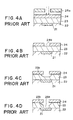
- Figs. 4A to 4D show cross sectional views respectively at the processes of the conventional hole forming method.
- a first conductive layer 21 is formed in the surface part of a semiconductor substrate 22.
- a second conductive layer (not shown) is formed thereon as a wiring layer.
- a contact hole is formed by the following manner.
- a resist film 24 is formed on the surface of the insulating film 23. Then it is subjected to an exposure using a photo mask 25a (Fig. 4A) having a mask pattern corresponding to a contact hole.
- a developing process is carried out to selectively remove an area 24a of the resist film 24 where a contact hole is to be formed (Fig. 4B).
- an isotropic etching is carried out to remove a surface part 23b of the insulating film 23 (Fig. 4C).
- An anisotropic etching process such as a reactive ion etching (RIE) is carried out to form a contact hole 23a in the first insulating film 23 (Fig. 4D).
- RIE reactive ion etching
- a second conductive layer 26 as an interconnection layer is formed on the surface of the insulating film 23 to thereby contact the second conductive layer 26 to the first conductive layer 21.
- an inclined portion is formed at the peripheral area 23b of the contact hole 23a by means of isotropic etching, and thereafter anisotropic etching is carried out to form the contact hole 23a.
- the distance between holes and the like must be shortened.
- a method of manufacturing a semiconductor device comprising the steps of: forming an insulating film on the surface of a semiconductor substrate; depositing a resist film on the surface of the insulating film; exposing the resist film for a first time by using a first mask having a pattern corresponding to a contact hole to be formed in the insulating film; exposing the resist film for a second time by using a second mask having a pattern corresponding to the contact hole and to an inclined portion to be formed at the peripheral portion of the contact hole; developing the resist film to remove a portion of the resist film corresponding to the contact hole and leave a portion having a thinner film thickness of the resist film corresponding to the inclined portion to be formed at the peripheral portion; and etching the insulating film to form the contact hole and the inclined portion at the peripheral portion respectively in the insulating film.
- a resist film is exposed by using two types of masks for appropriate exposure times, one corresponding to a contact hole and the other corresponding to the contact hole and an inclined portion to be formed at the peripheral portion of the contact hole, to thereby remove the portion of the resist film corresponding to the contact hole and leave the portion having a thinner film thickness of the resist film corresponding to the inclined portion.
- an insulating film is etched so that the portion of the insulating film corresponding to the contact hole is etched and the inclined portion is formed because of a presence of the resist film having a thinner film thickness. In this manner, a contact hole having an inclined portion at only a desired area can be formed, thereby allowing the distance between contact holes to be shortened and realize miniaturization of device elements, and further preventing an increase of the number of steps and improving throughput.
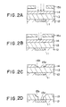
- Figs. 1A to 1D are cross sectional views of a device element at respective processes of the manufacturing method according to the embodiment.
- a first conductive region 11 formed in the surface part of a semiconductor substrate 12 there is formed an insulating film 13 on which further formed is a resist film 14.
- This resist film 14 is subjected to an exposure process using a first mask 15a having a pattern corresponding to a contact hole. This exposure is performed for a first time period shorter than the time period necessary for complete exposure by a second time period (Fig. 1A).
- the first mask 15a is replaced with a second mask 15b to again carry out an exposure process of the resist film 14 (Fig. 1B).
- This second mask 15b has a pattern corresponding not only to the contact hole itself but also to an inclined portion at the peripheral portion of the contact hole. This exposure is performed for the second time period.
- a portion 14a where the contact hole is to be formed is removed from the resist film 14, and there is left a portion 14b having a thinner film thickness where the inclined portion is to be formed (Fig. 1C).
- the processes starting from the resist coating process to the development process can be performed with the same processing apparatus.
- an anisotropic etching such as RIE is carried out.
- the portion of the insulating film 13 under the opening portion 14a without the resist film is first etched, and then the portion 14b having the thinner film thickness of the resist film 14 where the inclined portion is to be formed is etched, and thereafter the insulating film 13 under the portion 14 is gradually etched. Therefore, as shown in Fig. 1D, the insulating film 13 is formed such that it has a contact hole 13a and an inclined portion 13b at a particular peripheral portion thereof.
- the etching selection ratio is set to 5 and the second time duration is set such that the resist film 14b having a thickness of 0.1 ⁇ m is left at the region where the inclined portion is to be formed.
- the contact hole 13a and its inclined portion 13b are shown in the perspective view of Fig. 3. Different from a conventional contact hole, the contact hole is not radially formed at the same distance from the center, but it is formed only in a particular direction. As a result, even if the distance between contact holes is shortened, contact holes will not be short-circuited thereby realizing miniaturization of device elements.
- This method requires only one etching process and one resist depositing and developing process.
- a conventional method requires two lithography processes and two etching processes. Thus, the number of processes is reduced with an additional time period only required for mask replacement and exposure, thereby improving throughput.
- the exposure process using the first mask shown in Fig. 1A may be carried out after the exposure process using the second mask shown in Fig. 1B as shown in Figs. 2A-2D.
- the order of these exposure processes is determined in accordance with the photosensitive characteristic of a resist.
- the present invention is applicable to a method of forming holes in areas each having a different insulating film thickness and a different etching amount.
Abstract
In a method of manufacturing a semiconductor device, an insulating film (13) is formed on the surface of a semiconductor substrate (12); a resist film (14) is deposited on the surface of the insulating film (13); the resist film (14) is exposed for a first time by using a first mask (15a) having a pattern corresponding to a contact hole to be formed in the insulating film; the resist film (14) is exposed for a second time by using a second mask (15b) having a pattern corresponding to the contact hole (13a) and to an inclined portion (13b) to be formed at the peripheral portion of the contact hole; the resist film (14) is developed to remove a portion of the resist film corresponding to the contact hole (13a) and leave a portion having a thinner film thickness of the resist film corresponding to the inclined portion (13b) to be formed at the peripheral portion; and the insulating film (13) is etched to form the contact hole and the inclined portion at the peripheral portion respectively in the insulating film. The exposure processes using the first mask and the second mask are interchangeable.
Description
- The present invention relates to a method of manufacturing semi conductor devices, and more particularly to a method of forming contact holes.
- A conventional method of forming contact holes will be described.
- Figs. 4A to 4D show cross sectional views respectively at the processes of the conventional hole forming method. As shown in Fig. 4A, a first
conductive layer 21 is formed in the surface part of asemiconductor substrate 22. After aninsulating film 23 is formed on the surface of the firstconductive layer 21, a second conductive layer (not shown) is formed thereon as a wiring layer. In order to have an electrical connection between the second conductive layer and the firstconductive layer 21, it becomes necessary to form a contact hole in theinsulating film 23. In order to improve step coverage of the second conductive layer, the periphery of the contact hole is made inclined. Such a contact hole is formed by the following manner. - A
resist film 24 is formed on the surface of theinsulating film 23. Then it is subjected to an exposure using aphoto mask 25a (Fig. 4A) having a mask pattern corresponding to a contact hole. - A developing process is carried out to selectively remove an area 24a of the
resist film 24 where a contact hole is to be formed (Fig. 4B). - In order for a contact hole to have an inclined or rounded periphery, an isotropic etching is carried out to remove a
surface part 23b of the insulating film 23 (Fig. 4C). - An anisotropic etching process such as a reactive ion etching (RIE) is carried out to form a
contact hole 23a in the first insulating film 23 (Fig. 4D). - As shown in Fig. 5, after the
resist film 24 is removed, a secondconductive layer 26 as an interconnection layer is formed on the surface of theinsulating film 23 to thereby contact the secondconductive layer 26 to the firstconductive layer 21. - As described above, in the conventional method, an inclined portion is formed at the
peripheral area 23b of thecontact hole 23a by means of isotropic etching, and thereafter anisotropic etching is carried out to form thecontact hole 23a. - There are the following problems, however, associated with such a conventional contact hole forming method.
- In order to miniaturize a device element, the distance between holes and the like must be shortened. For this purpose, it is necessary to form an inclined area at a particular peripheral portion of the
contact hole 23a. If theperipheral portion 23b of the contact hole is removed by means of isotropic etching, the inclined portion of thecontact hole 23a is radially formed at the same distance from the center of thehole 23a, so that if the distance between contact holes is short, they may sometimes be electrically connected to each other. Thus, the work precision is lowered and a short-circuit occurs between interconnections. Furthermore, it is necessary to have an alignment margin between the contact hole and the conductive layer sufficiently larger than the diameter of the inclined portion, so that the distance between contact holes cannot be shortened, thus hindering miniaturization of device elements. - In addition, with the above conventional hole forming method, in order for a contact hole to have an inclined portion in a particular direction, it is necessary to provide at least two processes of removing insulating films, the process of making an inclined portion at the periphery of the contact hole, and the process of forming the contact hole. Namely, it is necessary to provide a lithography and etching process for making the inclined portion and a lithography and etching process for forming a contact hole, thus increasing the number of processes and lowering throughput.
- It is therefore an object of the present invention to provide a method of manufacturing a semiconductor device capable of miniaturizing device elements while minimizing an increase in the number of processes.
- According to the present invention, there is provided a method of manufacturing a semiconductor device comprising the steps of: forming an insulating film on the surface of a semiconductor substrate; depositing a resist film on the surface of the insulating film; exposing the resist film for a first time by using a first mask having a pattern corresponding to a contact hole to be formed in the insulating film; exposing the resist film for a second time by using a second mask having a pattern corresponding to the contact hole and to an inclined portion to be formed at the peripheral portion of the contact hole; developing the resist film to remove a portion of the resist film corresponding to the contact hole and leave a portion having a thinner film thickness of the resist film corresponding to the inclined portion to be formed at the peripheral portion; and etching the insulating film to form the contact hole and the inclined portion at the peripheral portion respectively in the insulating film.
- A resist film is exposed by using two types of masks for appropriate exposure times, one corresponding to a contact hole and the other corresponding to the contact hole and an inclined portion to be formed at the peripheral portion of the contact hole, to thereby remove the portion of the resist film corresponding to the contact hole and leave the portion having a thinner film thickness of the resist film corresponding to the inclined portion. By using the resist film thus formed, an insulating film is etched so that the portion of the insulating film corresponding to the contact hole is etched and the inclined portion is formed because of a presence of the resist film having a thinner film thickness. In this manner, a contact hole having an inclined portion at only a desired area can be formed, thereby allowing the distance between contact holes to be shortened and realize miniaturization of device elements, and further preventing an increase of the number of steps and improving throughput.
- In the accompanying drawings,
- Figs. 1A-1D are cross sectional views showing processes of a method of manufacturing a semiconductor device according to an embodiment of this invention;
- Figs. 2A-2D are cross sectional views showing processes of a method of manufacturing a semiconductor device according to another embodiment of this invention;
- Fig. 3 is a perspective view of a contact hole formed in accordance with the embodiment method;
- Figs. 4A-4D are cross sectional views at processes of a conventional method of manufacturing a semiconductor device; and
- Fig. 5 is a cross sectional view having a wiring layer on the contact hole formed by the method illustrated with Fig. 3.
- An embodiment of this invention will be described with reference to the accompanying drawings.
- Figs. 1A to 1D are cross sectional views of a device element at respective processes of the manufacturing method according to the embodiment. On a first
conductive region 11 formed in the surface part of asemiconductor substrate 12, there is formed aninsulating film 13 on which further formed is aresist film 14. This resistfilm 14 is subjected to an exposure process using afirst mask 15a having a pattern corresponding to a contact hole. This exposure is performed for a first time period shorter than the time period necessary for complete exposure by a second time period (Fig. 1A). - Then, the
first mask 15a is replaced with asecond mask 15b to again carry out an exposure process of the resist film 14 (Fig. 1B). Thissecond mask 15b has a pattern corresponding not only to the contact hole itself but also to an inclined portion at the peripheral portion of the contact hole. This exposure is performed for the second time period. - After a development process, a
portion 14a where the contact hole is to be formed is removed from theresist film 14, and there is left aportion 14b having a thinner film thickness where the inclined portion is to be formed (Fig. 1C). The processes starting from the resist coating process to the development process can be performed with the same processing apparatus. - Next, an anisotropic etching such as RIE is carried out. By properly setting the etching selection ratio, the portion of the
insulating film 13 under theopening portion 14a without the resist film is first etched, and then theportion 14b having the thinner film thickness of theresist film 14 where the inclined portion is to be formed is etched, and thereafter theinsulating film 13 under theportion 14 is gradually etched. Therefore, as shown in Fig. 1D, theinsulating film 13 is formed such that it has a contact hole 13a and aninclined portion 13b at a particular peripheral portion thereof. For example, if the etching portion having a depth of 0.5 µM is to be formed in the insulatingfilm 13 having a film thickness of 1.0 µm, the etching selection ratio is set to 5 and the second time duration is set such that the resistfilm 14b having a thickness of 0.1 µm is left at the region where the inclined portion is to be formed. - The contact hole 13a and its
inclined portion 13b are shown in the perspective view of Fig. 3. Different from a conventional contact hole, the contact hole is not radially formed at the same distance from the center, but it is formed only in a particular direction. As a result, even if the distance between contact holes is shortened, contact holes will not be short-circuited thereby realizing miniaturization of device elements. This method requires only one etching process and one resist depositing and developing process. A conventional method requires two lithography processes and two etching processes. Thus, the number of processes is reduced with an additional time period only required for mask replacement and exposure, thereby improving throughput. - The above-described embodiment has been given for the illustrative purposes only, and is not intended to limit the scope of this invention. For example, the exposure process using the first mask shown in Fig. 1A may be carried out after the exposure process using the second mask shown in Fig. 1B as shown in Figs. 2A-2D. The order of these exposure processes is determined in accordance with the photosensitive characteristic of a resist.
- Furthermore, the present invention is applicable to a method of forming holes in areas each having a different insulating film thickness and a different etching amount.
- Reference signs in the claims are intended for better understanding and shall not limit the scope.
Claims (2)
- A method of manufacturing a semiconductor device comprising the steps of:
forming an insulating film (13) on the surface of a semiconductor substrate (12);
depositing a resist film on the surface of said insulating film;
exposing said resist film' (14) for a first time by using a first mask (15a) having a pattern corresponding to a contact hole to be formed in said insulating film;
exposing said resist film for a second time by using a second mask (15b) having a pattern corresponding to said contact hole and to an inclined portion to be formed at the peripheral portion of said contact hole;
developing said resist film to remove a portion of said resist film corresponding to said contact hole and leave a portion having a thinner film thickness of said resist film corresponding to said inclined portion to be formed at said peripheral portion; and
etching said insulating film to form said contact hole and said inclined portion at said peripheral portion respectively in said insulating film. - A method of manufacturing a semiconductor device comprising the steps of:
forming an insulating film (13) on the surface of a semiconductor substrate (12);
depositing a resist film on the surface of said insulating film;
exposing said resist film (14) for a first time by using a first mask (15b) having a pattern corresponding to a contact hole to be formed in said insulating film and to an inclined portion to be formed at the peripheral portion of said contact hole;
exposing said resist film for a second time by using a second mask (15a) having a pattern corresponding to said contact hole;
developing said resist film to remove a portion of said resist film corresponding to said contact hole and leave a portion having a thinner film thickness of said resist film corresponding to said inclined portion to be formed at said peripheral portion; and
etching said insulating film to form said contact hole and said inclined portion at said peripheral portion respectively in said insulating film.
Applications Claiming Priority (2)
| Application Number | Priority Date | Filing Date | Title |
|---|---|---|---|
| JP65669/90 | 1990-03-16 | ||
| JP6566990A JPH03266437A (en) | 1990-03-16 | 1990-03-16 | Manufacture of semiconductor device |
Publications (2)
| Publication Number | Publication Date |
|---|---|
| EP0446939A2 true EP0446939A2 (en) | 1991-09-18 |
| EP0446939A3 EP0446939A3 (en) | 1994-03-30 |
Family
ID=13293639
Family Applications (1)
| Application Number | Title | Priority Date | Filing Date |
|---|---|---|---|
| EP91104008A Withdrawn EP0446939A2 (en) | 1990-03-16 | 1991-03-15 | Method of manufacturing semiconductor device |
Country Status (3)
| Country | Link |
|---|---|
| EP (1) | EP0446939A2 (en) |
| JP (1) | JPH03266437A (en) |
| KR (1) | KR950000090B1 (en) |
Families Citing this family (1)
| Publication number | Priority date | Publication date | Assignee | Title |
|---|---|---|---|---|
| US20050130075A1 (en) * | 2003-12-12 | 2005-06-16 | Mohammed Shaarawi | Method for making fluid emitter orifice |
Citations (4)
| Publication number | Priority date | Publication date | Assignee | Title |
|---|---|---|---|---|
| EP0034483A2 (en) * | 1980-02-14 | 1981-08-26 | Fujitsu Limited | Process for patterning a layer, for forming a contact through hole |
| US4714686A (en) * | 1985-07-31 | 1987-12-22 | Advanced Micro Devices, Inc. | Method of forming contact plugs for planarized integrated circuits |
| US4727045A (en) * | 1986-07-30 | 1988-02-23 | Advanced Micro Devices, Inc. | Plugged poly silicon resistor load for static random access memory cells |
| EP0315421A1 (en) * | 1987-11-05 | 1989-05-10 | Fujitsu Limited | Semiconductor integrated circuit device having at least two contact holes |
Family Cites Families (2)
| Publication number | Priority date | Publication date | Assignee | Title |
|---|---|---|---|---|
| JPS63258022A (en) * | 1987-04-15 | 1988-10-25 | Rohm Co Ltd | Manufacture of semiconductor device |
| JPH0237707A (en) * | 1988-07-27 | 1990-02-07 | Nec Corp | Manufacture of semiconductor device |
-
1990
- 1990-03-16 JP JP6566990A patent/JPH03266437A/en active Pending
-
1991
- 1991-03-14 KR KR1019910004026A patent/KR950000090B1/en not_active IP Right Cessation
- 1991-03-15 EP EP91104008A patent/EP0446939A2/en not_active Withdrawn
Patent Citations (4)
| Publication number | Priority date | Publication date | Assignee | Title |
|---|---|---|---|---|
| EP0034483A2 (en) * | 1980-02-14 | 1981-08-26 | Fujitsu Limited | Process for patterning a layer, for forming a contact through hole |
| US4714686A (en) * | 1985-07-31 | 1987-12-22 | Advanced Micro Devices, Inc. | Method of forming contact plugs for planarized integrated circuits |
| US4727045A (en) * | 1986-07-30 | 1988-02-23 | Advanced Micro Devices, Inc. | Plugged poly silicon resistor load for static random access memory cells |
| EP0315421A1 (en) * | 1987-11-05 | 1989-05-10 | Fujitsu Limited | Semiconductor integrated circuit device having at least two contact holes |
Also Published As
| Publication number | Publication date |
|---|---|
| EP0446939A3 (en) | 1994-03-30 |
| JPH03266437A (en) | 1991-11-27 |
| KR950000090B1 (en) | 1995-01-09 |
Similar Documents
| Publication | Publication Date | Title |
|---|---|---|
| JPS6260813B2 (en) | ||
| KR100443064B1 (en) | Image Reversal Method for Forming Small Scale Structures in Integrated Circuits | |
| EP0459252A2 (en) | Method of forming a thin film pattern with a trapezoidal cross section | |
| EP0540261B1 (en) | Process of removing polymers in semiconductor vias | |
| US20030003401A1 (en) | Technique for the size reduction of vias and other images in semiconductor chips | |
| US5679499A (en) | Method for forming photo mask for use in fabricating semiconductor device | |
| EP0446939A2 (en) | Method of manufacturing semiconductor device | |
| US6844143B2 (en) | Sandwich photoresist structure in photolithographic process | |
| US6372647B1 (en) | Via masked line first dual damascene | |
| CA1088382A (en) | Method of making a large scale integrated device having a planar surface | |
| US5338397A (en) | Method of forming a semiconductor device | |
| KR0170942B1 (en) | Flat conductor pattern forming method | |
| KR100226726B1 (en) | Method for forming metal interconnection layer of semiconductor device | |
| KR100257770B1 (en) | Method for forming fine conduction film of semiconductor device | |
| KR100235936B1 (en) | Method for manufacturing resist pattern | |
| KR100239435B1 (en) | Semiconductor manufacturing method | |
| KR0166488B1 (en) | Fine contact forming method in the semiconductor device | |
| KR100396689B1 (en) | Method for manufacturing gate of semiconductor device | |
| JP2980061B2 (en) | Method for manufacturing semiconductor device | |
| KR910001193B1 (en) | Semiconductor device | |
| KR100442288B1 (en) | Cell mask of semiconductor device and method for fabricating the same | |
| KR0147716B1 (en) | Formation method of elf alignment contact | |
| KR19990019502A (en) | Manufacturing Method of Semiconductor Device | |
| KR20010063661A (en) | Method of forming a damascene pattern in a semiconductor device | |
| KR19980058461A (en) | Manufacturing method of semiconductor device |
Legal Events
| Date | Code | Title | Description |
|---|---|---|---|
| PUAI | Public reference made under article 153(3) epc to a published international application that has entered the european phase |
Free format text: ORIGINAL CODE: 0009012 |
|
| 17P | Request for examination filed |
Effective date: 19910315 |
|
| AK | Designated contracting states |
Kind code of ref document: A2 Designated state(s): DE FR GB |
|
| PUAL | Search report despatched |
Free format text: ORIGINAL CODE: 0009013 |
|
| AK | Designated contracting states |
Kind code of ref document: A3 Designated state(s): DE FR GB |
|
| STAA | Information on the status of an ep patent application or granted ep patent |
Free format text: STATUS: THE APPLICATION HAS BEEN WITHDRAWN |
|
| 18W | Application withdrawn |
Withdrawal date: 19950719 |