EP0447856A1 - Nonvolatile semiconducteur memory - Google Patents
Nonvolatile semiconducteur memory Download PDFInfo
- Publication number
- EP0447856A1 EP0447856A1 EP91103051A EP91103051A EP0447856A1 EP 0447856 A1 EP0447856 A1 EP 0447856A1 EP 91103051 A EP91103051 A EP 91103051A EP 91103051 A EP91103051 A EP 91103051A EP 0447856 A1 EP0447856 A1 EP 0447856A1
- Authority
- EP
- European Patent Office
- Prior art keywords
- blocks
- data
- floating gate
- lines
- memory
- Prior art date
- Legal status (The legal status is an assumption and is not a legal conclusion. Google has not performed a legal analysis and makes no representation as to the accuracy of the status listed.)
- Granted
Links
- 239000004065 semiconductor Substances 0.000 claims abstract description 9
- 238000002347 injection Methods 0.000 claims abstract description 3
- 239000007924 injection Substances 0.000 claims abstract description 3
- 238000003491 array Methods 0.000 claims description 6
- 239000011159 matrix material Substances 0.000 claims description 4
- 238000009413 insulation Methods 0.000 claims 1
- 239000010410 layer Substances 0.000 description 22
- 101150068401 BSL1 gene Proteins 0.000 description 8
- 238000010586 diagram Methods 0.000 description 8
- 238000009792 diffusion process Methods 0.000 description 5
- 229910021420 polycrystalline silicon Inorganic materials 0.000 description 5
- 229920005591 polysilicon Polymers 0.000 description 5
- 101150011571 BSL2 gene Proteins 0.000 description 4
- 102100031885 General transcription and DNA repair factor IIH helicase subunit XPB Human genes 0.000 description 3
- 101000920748 Homo sapiens General transcription and DNA repair factor IIH helicase subunit XPB Proteins 0.000 description 3
- 101100049574 Human herpesvirus 6A (strain Uganda-1102) U5 gene Proteins 0.000 description 3
- 230000000694 effects Effects 0.000 description 3
- 101150064834 ssl1 gene Proteins 0.000 description 3
- 101150062870 ssl3 gene Proteins 0.000 description 3
- 230000005684 electric field Effects 0.000 description 2
- 239000002784 hot electron Substances 0.000 description 2
- 238000000034 method Methods 0.000 description 2
- 239000000758 substrate Substances 0.000 description 2
- 101100272788 Arabidopsis thaliana BSL3 gene Proteins 0.000 description 1
- XAGFODPZIPBFFR-UHFFFAOYSA-N aluminium Chemical compound [Al] XAGFODPZIPBFFR-UHFFFAOYSA-N 0.000 description 1
- 229910052782 aluminium Inorganic materials 0.000 description 1
- 239000003990 capacitor Substances 0.000 description 1
- 238000007796 conventional method Methods 0.000 description 1
- 239000011229 interlayer Substances 0.000 description 1
- 230000007774 longterm Effects 0.000 description 1
- 230000003071 parasitic effect Effects 0.000 description 1
- 238000004904 shortening Methods 0.000 description 1
Images


Classifications
-
- G—PHYSICS
- G11—INFORMATION STORAGE
- G11C—STATIC STORES
- G11C16/00—Erasable programmable read-only memories
- G11C16/02—Erasable programmable read-only memories electrically programmable
-
- G—PHYSICS
- G11—INFORMATION STORAGE
- G11C—STATIC STORES
- G11C16/00—Erasable programmable read-only memories
- G11C16/02—Erasable programmable read-only memories electrically programmable
- G11C16/06—Auxiliary circuits, e.g. for writing into memory
- G11C16/10—Programming or data input circuits
- G11C16/14—Circuits for erasing electrically, e.g. erase voltage switching circuits
- G11C16/16—Circuits for erasing electrically, e.g. erase voltage switching circuits for erasing blocks, e.g. arrays, words, groups
-
- H—ELECTRICITY
- H01—ELECTRIC ELEMENTS
- H01L—SEMICONDUCTOR DEVICES NOT COVERED BY CLASS H10
- H01L29/00—Semiconductor devices adapted for rectifying, amplifying, oscillating or switching, or capacitors or resistors with at least one potential-jump barrier or surface barrier, e.g. PN junction depletion layer or carrier concentration layer; Details of semiconductor bodies or of electrodes thereof ; Multistep manufacturing processes therefor
- H01L29/40—Electrodes ; Multistep manufacturing processes therefor
- H01L29/41—Electrodes ; Multistep manufacturing processes therefor characterised by their shape, relative sizes or dispositions
- H01L29/423—Electrodes ; Multistep manufacturing processes therefor characterised by their shape, relative sizes or dispositions not carrying the current to be rectified, amplified or switched
- H01L29/42312—Gate electrodes for field effect devices
- H01L29/42316—Gate electrodes for field effect devices for field-effect transistors
- H01L29/4232—Gate electrodes for field effect devices for field-effect transistors with insulated gate
- H01L29/42324—Gate electrodes for transistors with a floating gate
- H01L29/42328—Gate electrodes for transistors with a floating gate with at least one additional gate other than the floating gate and the control gate, e.g. program gate, erase gate or select gate
-
- H—ELECTRICITY
- H10—SEMICONDUCTOR DEVICES; ELECTRIC SOLID-STATE DEVICES NOT OTHERWISE PROVIDED FOR
- H10B—ELECTRONIC MEMORY DEVICES
- H10B69/00—Erasable-and-programmable ROM [EPROM] devices not provided for in groups H10B41/00 - H10B63/00, e.g. ultraviolet erasable-and-programmable ROM [UVEPROM] devices
Definitions
- the present invention relates to a nonvolatile semiconductor memory whose data can be electrically erased, and more particularly, to a nonvolatile semiconductor memory capable of preventing erroneous operation of non-selected cells by shortening the time during which a voltage stress is applied to the non-selected cells.
- An Electrically Erasable and Programmable ROM can electrically erase and write data by using an electric signal while it is mounted on a circuit board. Therefore, it is more useful than an EEPROM of an ultraviolet erase type.
- Demand for EEPROMs is therefore rapidly increasing for use with control circuits, IC cards (memory cards), and the like.
- IC cards memory cards
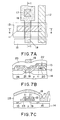
- its memory cell has the structure such as shown in Figs. 7A to 7C.
- Fig. 7A is a plan view showing a pattern layout
- Fig. 7B is a cross sectional view taken along line B-B of Fig. 7A
- Fig. 7C is a cross sectional view taken along line C-C of Fig. 7A.
- reference numeral 11 represents a floating gate made of a polysilicon first layer.
- Reference numeral 12 represents an erase gate made of a polysilicon second layer.
- Reference numeral 13 represents a control gate made of a polysilicon third layer. The control gate 13 is also used as a word line.
- Reference numeral 14 represents a P-type substrate.
- Reference numerals 15 and 16 represent a source and a drain made of an N+-type diffusion layer and formed on the substrate 14, respectively.
- Reference numeral 17 represents a contact hole.
- Reference numeral 18 represents a data line made of an aluminum layer connected to the drain 16 via the contact hole 17.
- Reference numeral 19 represents a gate insulating film at the floating gate transistor region having a thickness of 300 angstroms.
- Reference numeral 20 represents a gate insulating film having a thickness of 350 angstroms and formed between the floating gate 11 and the erase gate 12.
- Reference numeral 21 represents a gate insulating film formed between the floating gate 11 and the control gate 13. This gate insulating film 21 is made of a three-layer structure film having an Oxide-Nitride-Oxide (O-N-O) structure.
- Reference numeral 22 represents a gate insulating film formed between the erase gate 12 and the control gate 13 and also having the O-N-O structure.
- Reference numeral 23 represents a gate insulating film at a select transistor region which uses the polysilicon layer 13 as its gate electrode.
- Reference numeral 24 represents a field insulating film, and 25 represents an interlayer insulating film.
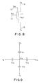
- FIG. 8 The equivalent circuit of the memory cell shown in Figs. 7A to 7C is shown in Fig. 8, and the equivalent circuit of the capacitance system is shown in Fig. 9.
- V D represents a drain potential
- V S a source potential
- V EG an erase gate potential
- V CG a control gate potential
- C FC represents a capacitance between the floating gate 11 and the control gate 13
- C FE a capacitance between the floating gate 11 and the erase gate 12
- C FD a capacitance between the floating gate 11 and the drain 16
- C FS another capacitance as viewed from the floating gate 11.
- the initial value Q (I) of electrical charge stored in all capacitors is given by the following equation.
- Q (I) (V FG - V CG )
- C T C FC + C FE + C FD + C FS (2)
- V FG ⁇ (V CG C FC + V EG C FE + V D C FD + V S C FS )/C T ⁇ + ⁇ Q (I) /C T ⁇ (3)
- V FG ⁇ (V CG C FC + V EG C FE + V D C FD )/C T ⁇ + V FG(I) (4)
- Memory cells each constructed as above are actually disposed in a matrix within a memory cell array.
- a four bit memory array having four memory cells M1 to M4 is shown in Fig. 10.
- Each of the drains 16 of the four memory cells M1 to M4 is connected to two data lines DL1 and DL2.
- Each of the control gates 13 is connected to two word lines WL1 and WL2.
- the erase gates 12 are commonly connected to one erase line EL, and the sources are applied with a reference voltage (e.g., 0 V).
- the source potential V S , drain potential V D , and control gate potential V CG of each memory cell are set to 0 V (namely, the data lines DL1 and DL2, and word lines WL1 and WL2 are set to 0 V), and the erase gate potential V EG is set to a high potential (e.g., +20 V).
- the Fowler-Nordheim's tunnel effect electrons in the floating gate 11 are emitted to the erase gate 12 by the electric field so that the floating gate 11 is charged positive.
- the control gate potential V CG potential at the word line WL1 for the selected memory cell M1 is set to a high potential, e.g., +12.5 V
- the drain potential V D potential at the data line DL1 is set to a high potential, e.g., +10 V
- the source voltage V S potentials at the data line DL2 and word line WL2 are set to 0 V.
- the erase gate potential V FG is set to +5 V for example so that the potential at the floating gate 11 rises to alleviate writing data into the selected cell M1.
- the hot electron effect occurs near the drain 16 of the selected cell M1 so that electrons generated by impact ionization are injected into the floating gate 11.
- the floating gate potential V FG With the control gate potential V CG of 12.5 V, the floating gate potential V FG will become 10.5 V according to the equation (4).
- the potential at the erase gate 12 as seen from the floating gate 11 is -5.5 V because the erase gate potential V EG is 5 V.
- electrical field is relaxed relative to the erase gate at the floating gate of a non-selected cell M2 connected to the same word line as that of the selected cell M1. Accordingly, erroneous operation due to erroneous data writing can be avoided, resulting in improved reliability.
- the maximum voltage stress to the floating gate among non-selected memory cells M2 to M4 in Fig. 10 is applied to the non-selected memory cell M3 when it has data "0", the control gate thereof being connected to the word line WL2 different from the word line WL1 of the selected memory cell M1.
- a voltage of +13.0 V is applied between the floating gate 11 and drain 16 of the non-selected cell M3. Electrons in the floating gate 11 are therefore likely to be emitted to the drain, and in some cases there is a fear of erroneously erasing the data.
- the case, second likely to be operated erroneously, is for the memory cell M2 when it has data "1". In this case, electrons are likely to be injected into the floating gate, resulting in a fear of writing data erroneously.
- Fig. 11 is a circuit diagram showing a conventional memory having memory cells described above.
- each of cells 30 in a memory cell array 31 is connected to n data lines DL1 to DLn, and each control gate 13 is connected to m word lines WL1 to WLm.
- Erase gates 12 of the memory cells 30 are commonly connected to an erase line EL, and a reference voltage, e.g., 0 V is applied to the sources 15.
- the erase gates of all the memory cells 30 in the memory cell array are commonly connected so that a voltage V EG is applied to the erase gates of all the memory cells 30 at the same time when data is written.
- V EG voltage
- reference numeral 32 represents a row decoder, 33 a column decoder, 34-1 to 34-n column select transistors, 35 a bus line, 36 a data input circuit, 37 a sense amplifier circuit, 38 a data output circuit, 39 an erase voltage booster circuit, and 41 an address buffer.
- the maximum time while a stress is applied to a non-selected memory cell becomes (m-1) x t per one bit (one cell) (for example, the stress time for a non-selected memory cell M3 in the possible erroneous data erase state as described with Table 1, is the time duration while the control gate 13 is applied with 0 V and the drain 16 is applied with 10 V).
- the maximum time while a stress is applied to a non-selected memory cell becomes (n-1) x t per one bit (one cell) (for example, the stress time for a non-selected memory cell M2 in the possible erroneous data write state as described with Table 1, is the time duration while the control gate 13 is applied with 12.5 V and the drain 16 is applied with 0 V).
- m represents the number of rows
- n represents the number of columns.
- a data write time for one bit is 1 ms
- Figs. 12A to 12C show a second example of a conventional EEPROM cell having no erase gate. Like elements to those in Figs. 7A to 7C are given identical reference numerals. Points of difference from the EEPROM shown in Figs. 7A to 7C reside in that the EEPROM shown in Figs. 12A to 12C has no erase gate and no select transistor having the control gate 13 as its gate, and the floating gate 11 is in direct contact with the source 15 and drain 16.
- the floating gate insulating film 19 is formed as thin as about 100 angstroms.
- the source 15 is applied with an erase voltage of 10 V, the drain 16 is made to enter a floating state, and the control gate 13 is set to 0 V.
- a high voltage is applied via the thin floating insulating film 19 across the floating gate 11 and source 15. In this condition, by the Fowler-Nordheim's tunnel effect, electrons in the floating gate 11 are emitted to the source 15 to thereby erase the data.
- the drain 16 is set to about 6 V, the source to 0 V, and the control gate 13 to 12 V. In this condition, hot electrons generated near at the drain 16 are injected into the floating gate 11 to thereby write the data.
- the drain 16 In reading data, the drain 16 is set to 1 V, the source 15 to 0 V, and the control gate 13 to 5 V. In this condition, the data "0" or "1" is read which is determined in accordance with whether or not electrons are present in the floating gate 11.
- Memory cells described above may also be used in place of memory cells shown in Fig. 11 to form a memory cell array.
- the erase lines EL are connected to the sources V S common for all memory cells. In this arrangement, data can be erased collectively for all memory cells.
- the memory cell area is divided into a plurality of small sub-areas (hereinafter called blocks) and data is erased on the block unit basis (hereinafter called block erase).
- block erase erase gates of memory cells connected to two word lines are coupled together.
- V EG 20 V by means of an erase decoder (not shown). In this manner, only memory cells belonging to the selected block can be erased, thus allowing block erase.
- the EEPROM in Figs. 12A to 12C shown as the second conventional example has its memory cell constructed by using only two polysilicon layers so that it is suitable for miniaturization.
- the insulating film 19 in particular is as thin as 100 angstroms so that practical block erase is difficult.
- the present invention has been made while considering the above problems. It is therefore an object of this invention to provide a non-volatile semiconductor memory wherein the memory cell array is divided into a plurality of blocks and a stress is not allowed to be applied to non-selected blocks during data write to thereby prevent erroneous operation of non-selected memory cells during the data write.
- the non-volatile semiconductor memory cell comprises: a plurality of blocks each having a plurality of floating gate transistors as memory cells, the floating gate transistor having a drain, a source, a floating gate, and a control gate capacitively coupled to the floating gate, and a data program of the floating gate transistor being effected by data write through injection of electrons into the floating gate and by data erase through emission of electrons from the floating gates; means for applying an erase signal to a selected one of the blocks to emit electrons from the floating gates of a plurality of memory cells in the selected block and to erase data in all of said memory cells in said selected block at the same time; and means for applying an erase signal to the drains of the floating transistors in the selected block, without applying the write signal to the drains of the floating gate transistors in non-selected blocks.
- a memory cell array is divided into a plurality of blocks to erase data in the block unit basis and to prevent a voltage stress to non-selected blocks during data write.
- the embodiments realize high reliability of W/E cycles.
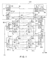
- Fig. 1 shows the first embodiment of this invention.
- like elements to those shown in Fig. 11 are represented by identical reference numerals and symbols of Fig. 1.
- Ac represents a column address
- Ar a row address
- Ae an erase address
- a BS a block select address.
- Each memory cell array 31-1 to 31-k is a set (block) of memory cells connected to a plurality of word lines (in this case, two word lines).
- the word lines of each block is connected to the corresponding one of row decoders 32-1 to 32-k.
- erase gates of a plurality of memory cells are commonly connected, and the commonly connected erase gate are connected to the corresponding one of the erase lines EL1 to ELk.
- Erase decoders 44-1 to 44-k are used to select a corresponding one of the erase lines EL1 to ELk.
- drains of a plurality of memory cells 30 in the same column are connected to a same common drain 43.
- This common drain 43 is connected, via the corresponding one of array select transistors 42-1 to 42-n, to the corresponding one of data lines DL1 to DLn. Gates of each of these block select transistors 42-1 to 42-n are connected to the corresponding one of block select lines BSL1 to BSLk. Each of these select lines BSL1 to BSLk is connected to the corresponding one of block select decoders 45-1 to 45-k.
- the other structure is substantially the same as that shown in Fig. 11.
- the erase decoder 44-1 is selected so that an erase voltage V EG (about 20 V) is applied to the erase line EL1.
- the other erase decoders 44-2 to 44-k are not selected, so the erase lines EL2 to ELk are set to 0 V.
- the word lines of all the arrays 31-1 to 31-k are set to 0 V, the block select lines BSL1 to BSLk are also set to 0 V, and the common drain 43 is set substantially to 0 V. As a result, all memory cells within the memory cell array 31-1 are erased at the same time.
- the non-selected block select lines BSL2 becomes 0 V. Therefore, all the block select transistors 42-1 to 42-n of the non-selected block cell arrays 31-2 to 31-k are being turned off. Accordingly, all the common drains 43 within the non-selected block cell arrays 31-2 to 31-k are generally 0 V (in a floating state). For this reason, a voltage stress is not applied to the drain of each cell 30 within the non-selected cell arrays 31-2 to 31-k.
- the block select decoder 45-1 is selected so that only the block select line BSL1 becomes 5 V.
- the other lines BSL2 to BSLk are not selected and become 0 V.
- the word line WL1 of the selected block 31-1 is selected by the row decoder 32-1 so that the word line WL1 becomes 5 V.
- the column select line CL1 is selected by the column decoder 33, the data line DL1 is selected. In this condition, the data is read from the selected memory cell M1. In this case, all the block select transistors 42-2 to 42-k of the non-selected blocks 31-2 to 31-k are being turned off.
- the common drains 43 of the other arrays 31-2 to 31-k are disconnected from the data line DL1 so that parasitic capacitance on the data line DL1 is considerably reduced.
- the charge/discharge time of the data line DL1 is shortened and data is read from the memory cell M1 at high speed. If the read speed is allowed to be slower than this, all the block select lines BSL1 to BSLk may be set to 5 V.
- the stress time of the memory cell M3 for example will be compared with that of the memory shown in Fig. 11, assuming that the memory of 1 M bits is constructed as shown in Fig. 1.
- the stress is applied to the memory cell M3 only when data is to be written in the cell M1 within the same block 31-1, and is not applied when data is to be written in any cell within the other blocks 31-2 to 31-k. Therefore, the stress time of the cell M3 is one data write time in the memory shown in Fig. 1 (wherein two word lines are connected to one row decoder). Assuming that the one data write time is 1 ms similar to the conventional case described above, the stress time is 1 ms which is extremely short as compared with 1.023 sec obtained by the equation (a) in the conventional memory. Consequently, the cell M3 is not erroneously erased in practice.
- Fig. 2 is a circuit diagram showing a part of the actual layout pattern similar to the circuit shown in Fig. 1.
- Figs. 3A to 3C are a plan view and cross sectional views of the circuit shown in Fig. 2. Namely, Fig. 3A is a plan view, Fig. 3B is a cross sectional view taken along line B-B of Fig. 2, and Fig. 3C is a cross sectional view taken along line C-C of Fig. 2.
- like elements to those shown in Figs. 7A to 7C are represented by identical reference numerals and symbols.
- drains 16 of the four memory cells are commonly connected by using only a diffusion layer 16A without contacting them directly to an A1 layer.
- the drains 16 commonly connected via the diffusion layer 16A are connected to the block select transistor 42-1.
- the diffusion layer 16A is connected to the data line (A1) DL 18 via a contact 17.
- only one contact hole is used for eight transistors, within two blocks, connected to one data line, reducing the number of contacts to one fourth the conventional memory per one block and contributing to efficiently reducing the pattern dimension.
- the sources 15 of a pair of cells 30 are commonly connected by using a diffusion layer 15A which is in turn connected to a V SS line (A1) 26 via a contact hole 17a.
- Fig. 4 shows another embodiment also capable of block erase.
- Fig. 4 corresponds to the memory without an erase gate shown in Figs. 12A to 12C.
- the different point of Fig. 4 from Fig. 2 is that there is formed a source select transistor 47 between a common source line V SS* and a common source 46 of memory cells within a block.
- the gates of these transistors 47 within a block are commonly connected to the corresponding one of source select lines SSL1 to SSLk (in Fig. 4, only SSL2 and SSL3 are shown).
- the circuit indicated by 100 shown in Figs. 4 and 6 is the same as the circuit 100 shown in Fig. 1.
- the block select line BSL2 and word lines WL5 to WL8 is set to 0 V, and the source select line SSL2 and common source line V SS* are set to 12 V.
- the source select lines SSL1, SSL3 to SSLk of the non-selected blocks are all set to 0 V. In this condition, there is applied about 10 V only to the common source line 46 of the selected block. On the other hand, an erase voltage is not applied to the sources of memory cells of the non-selected block to avoid data erase.
- the block select line BSL2 and source select line SSL2 are selected and become 12 V.
- the common source line V SS* becomes 0 V.
- data is written in the memory cell 30 (M1).
- the block select lines BSL1, BSL3 to BSLk of the other blocks are all set to 0 V, any stress is applied to the drains of memory cells 30 of the non-selected blocks even if the data line DL1 becomes 6 V.
- the source select lines SSL1, SSL3 to SSLk of the non-selected blocks be set to 0 V. However, even if the source select transistors are being turned on, there occurs no problem.
- Fig. 4A shows a device that enables a reduction of the width of the device of Fig. 4.
- the device shown in Fig. 4A is a single data system for two adjacent data lines shown in Fig. 4.
- the two data lines DL2 and DL3 of Fig. 4 becomes the one data line DL23.
- the two common drains 43, 43 positioned on each side of the two data lines that were one data line, become the one common drain 43A.
- the two common drains 43, 43 are made into the one common drain 43A and so the two array selector transistors that were respectively connected to the drains 43, 43 become one array selector transistor.
- the selector transistors 42-2 and 42-3 become the one array selector transistor 42-23.
- Fig. 4A shows a device that enables a reduction of the width of the device of Fig. 4.
- the device shown in Fig. 4A is a single data system for two adjacent data lines shown in Fig. 4.
- a common source line V SS*1 and V SS*2 between the two cells (for example M1 and M2) that are symmetrical left and right is formed a common source line V SS*1 and V SS*2 .
- the source voltage that is applied to those common source lines is determined by the source decoder SD.
- the source decoder SD has the array address A C (see Fig. 1), A C+1 and the erase signal Erase applied to it.
- the data write, read and erase operations in Fig. 4A are performed by applying a voltage to each of the lines in the same manner as shown in Fig. 4. However, in the case of Fig. 4A, the selection of the common source line for each of the operations differs from that for Fig. 4. More specifically, when there is erase, the Erase signal is applied to the source decoder SD. The source decoder SD applies 12 V to all of the common source lines V SS*1 and V SS*2 . In addition, when there is write, the array decoder 33 (see Fig. 1) makes the data line DL23 for example, 6V due to the array address A C .
- the source decoder makes the common source lines V SS*1 and V SS*2 for example, the 0 V and open status, respectively on the basis of the array addresses A C and A C+1 . All common source lines other than these are also in the open status.
- the data line 23 is selected, for example, only one of the common source lines V SS*1 and V SS*2 is made 0 V.
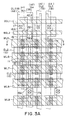
- Figs. 5A to 5C show the actual layout of the circuit shown in Fig. 4.
- Fig. 5A is a plan view
- Fig. 5B is a cross sectional view taken along line B-B of Fig. 4
- Fig. 5C is a cross sectional view taken along line C-C of Fig. 4.
- the fundamental layout shown in Figs. 5A to 5C is similar to that shown in Figs. 3A to 3C.
- the different points are that the common source line V SS* 27 is made of the second A1 layer, the data lines DL1 to DLn are made of the first A1 layer, and the common source line V SS* is disposed perpendicular to the data lines DL1 to DLn.
- this layout it is possible to determine the cell pitch in the lateral or row direction in accordance with the pitch of the first AL wirings of the data lines DL1 to DLn.
- the common source line V SS* may be made of the first A1 layer, and the data lines may be made of the second A1 layer. Furthermore, the common source line V SS* may be disposed in parallel with the data lines as shown in Figs. 3A to 3C. With such a layout, although a cell size becomes large more or less, wirings for the common source lines and data lines can be realized with a single A1 layer, thereby allowing easy processes.
- FIG. 6 Another embodiment is shown in Fig. 6. The different point from that shown in Fig. 4 is that instead of providing the source select line and source select transistor, source lines V SS*1 to V SS*k (only V SS*2 and V SS*3 are shown) dedicated to each block are provided to each memory common source 46.
- a high voltage is applied only to the common source line of a selected block.
- the block having the word lines WL5 to WL8 is selected, only the common source line V SS*2 is selected by an erase decoder (44-2) and applied with 10 V to erase the data of memory cells within the selected block.
- the common source lines V SS*1 , V SS*3 to V SS*k of the non-selected blocks are set to 0 V, and data erase is not carried out.
- the common source lines V SS*1 to V SS*k may be used in common in the column direction and disposed in parallel with the data lines DL1 to DLk, to allow wirings using only a single A1 layer and provide easy processes. In this case, block erase cannot be allowed, but all cells of the memory are collectively erased. If block erase is intended, the common source line V SS* is set to 10 V, only the word lines of the selected block, e.g., the word lines WL5 to WL8, are set to 0 V, and the word lines WL1 to WL4, WL9 to WLm of the other non-selected blocks are all set to 12 V.
- the voltage between the floating gate 11 and source 15 of a memory cell connected to the non-selected word line becomes considerably small as compared with that of the selected memory cell. Accordingly, the data in the memory cell connected to the non-selected word line is not erased, but only the data in the memory cell connected to the selected word line is erased.
Abstract
Description
- The present invention relates to a nonvolatile semiconductor memory whose data can be electrically erased, and more particularly, to a nonvolatile semiconductor memory capable of preventing erroneous operation of non-selected cells by shortening the time during which a voltage stress is applied to the non-selected cells.
- An Electrically Erasable and Programmable ROM (EEPROM) can electrically erase and write data by using an electric signal while it is mounted on a circuit board. Therefore, it is more useful than an EEPROM of an ultraviolet erase type. Demand for EEPROMs is therefore rapidly increasing for use with control circuits, IC cards (memory cards), and the like. In order to realize an EEPROM having a large capacity in particular, its memory cell has the structure such as shown in Figs. 7A to 7C.
- Fig. 7A is a plan view showing a pattern layout, Fig. 7B is a cross sectional view taken along line B-B of Fig. 7A, and Fig. 7C is a cross sectional view taken along line C-C of Fig. 7A. In these figures,
reference numeral 11 represents a floating gate made of a polysilicon first layer.Reference numeral 12 represents an erase gate made of a polysilicon second layer.Reference numeral 13 represents a control gate made of a polysilicon third layer. Thecontrol gate 13 is also used as a word line.Reference numeral 14 represents a P-type substrate.Reference numerals substrate 14, respectively.Reference numeral 17 represents a contact hole.Reference numeral 18 represents a data line made of an aluminum layer connected to thedrain 16 via thecontact hole 17.Reference numeral 19 represents a gate insulating film at the floating gate transistor region having a thickness of 300 angstroms.Reference numeral 20 represents a gate insulating film having a thickness of 350 angstroms and formed between thefloating gate 11 and theerase gate 12.Reference numeral 21 represents a gate insulating film formed between thefloating gate 11 and thecontrol gate 13. Thisgate insulating film 21 is made of a three-layer structure film having an Oxide-Nitride-Oxide (O-N-O) structure.Reference numeral 22 represents a gate insulating film formed between theerase gate 12 and thecontrol gate 13 and also having the O-N-O structure.Reference numeral 23 represents a gate insulating film at a select transistor region which uses thepolysilicon layer 13 as its gate electrode.Reference numeral 24 represents a field insulating film, and 25 represents an interlayer insulating film. - The equivalent circuit of the memory cell shown in Figs. 7A to 7C is shown in Fig. 8, and the equivalent circuit of the capacitance system is shown in Fig. 9. In Fig. 8, VD represents a drain potential, VS a source potential, VFG a floating gate potential, VEG an erase gate potential, and VCG a control gate potential. In Fig. 9, CFC represents a capacitance between the
floating gate 11 and thecontrol gate 13, CFE a capacitance between thefloating gate 11 and theerase gate 12, CFD a capacitance between thefloating gate 11 and thedrain 16, and CFS another capacitance as viewed from thefloating gate 11. In this capacitance system, the initial value Q(I) of electrical charge stored in all capacitors is given by the following equation.


- The total capacitance CT is given by the following equation.

- The voltage VFG applied to the floating gate is therefore given by the following equation.


- By substituting Q(i)/CT = VFG(i) and VS = 0 V into the equation (3), we obtain


- Memory cells each constructed as above are actually disposed in a matrix within a memory cell array. For simplicity of description, a four bit memory array having four memory cells M1 to M4 is shown in Fig. 10. Each of the
drains 16 of the four memory cells M1 to M4 is connected to two data lines DL1 and DL2. Each of thecontrol gates 13 is connected to two word lines WL1 and WL2. Theerase gates 12 are commonly connected to one erase line EL, and the sources are applied with a reference voltage (e.g., 0 V). - In the memory cell array constructed as above, data is erased collectively for all the memory cells M1 to M4. More in particular, the source potential VS, drain potential VD, and control gate potential VCG of each memory cell are set to 0 V (namely, the data lines DL1 and DL2, and word lines WL1 and WL2 are set to 0 V), and the erase gate potential VEG is set to a high potential (e.g., +20 V). In this case, by the Fowler-Nordheim's tunnel effect, electrons in the
floating gate 11 are emitted to theerase gate 12 by the electric field so that the floatinggate 11 is charged positive. Assuming that the potential VFG(I) of thefloating gate 11 rises for example to +3 V (assuming in this case the threshold voltage VTH of the floating gate transistor is 1 V), then an inversion layer is formed under thefloating gate 11 so that the threshold voltages of the memory cells M1 to M4 become lower. This state assumes that data "1" is being stored. - Consider next writing data in a selected memory cell, e.g., memory cell M1 in the memory cell array. In order to write data in the selected memory cell M1, the control gate potential VCG (potential at the word line WL1) for the selected memory cell M1 is set to a high potential, e.g., +12.5 V, the drain potential VD (potential at the data line DL1) is set to a high potential, e.g., +10 V, and the source voltage VS, and potentials at the data line DL2 and word line WL2 are set to 0 V. The erase gate potential VFG is set to +5 V for example so that the potential at the
floating gate 11 rises to alleviate writing data into the selected cell M1. The hot electron effect occurs near thedrain 16 of the selected cell M1 so that electrons generated by impact ionization are injected into thefloating gate 11. With the control gate potential VCG of 12.5 V, the floating gate potential VFG will become 10.5 V according to the equation (4). However, the potential at theerase gate 12 as seen from thefloating gate 11 is -5.5 V because the erase gate potential VEG is 5 V. By applying 5 V to theerase gate 12 as in the above case, electrical field is relaxed relative to the erase gate at the floating gate of a non-selected cell M2 connected to the same word line as that of the selected cell M1. Accordingly, erroneous operation due to erroneous data writing can be avoided, resulting in improved reliability. Apart from the above discussion, the voltage stress applied between thedrain 16 and the floating gate changes greatly with whether the data of a memory cell is "1" or "0". The voltage stresses applied between thedrain 16 and thefloating gate 11 of each of four memory cells M1 to M4 are summarized in Table 1.
- The maximum voltage stress to the floating gate among non-selected memory cells M2 to M4 in Fig. 10 is applied to the non-selected memory cell M3 when it has data "0", the control gate thereof being connected to the word line WL2 different from the word line WL1 of the selected memory cell M1. Specifically, as seen from Table 1, a voltage of +13.0 V is applied between the
floating gate 11 anddrain 16 of the non-selected cell M3. Electrons in the floatinggate 11 are therefore likely to be emitted to the drain, and in some cases there is a fear of erroneously erasing the data. The case, second likely to be operated erroneously, is for the memory cell M2 when it has data "1". In this case, electrons are likely to be injected into the floating gate, resulting in a fear of writing data erroneously. - Fig. 11 is a circuit diagram showing a conventional memory having memory cells described above. In Fig. 11, each of
cells 30 in amemory cell array 31 is connected to n data lines DL1 to DLn, and eachcontrol gate 13 is connected to m word lines WL1 to WLm. Erasegates 12 of thememory cells 30 are commonly connected to an erase line EL, and a reference voltage, e.g., 0 V is applied to thesources 15. The erase gates of all thememory cells 30 in the memory cell array are commonly connected so that a voltage VEG is applied to the erase gates of all thememory cells 30 at the same time when data is written. In Fig. 11,reference numeral 32 represents a row decoder, 33 a column decoder, 34-1 to 34-n column select transistors, 35 a bus line, 36 a data input circuit, 37 a sense amplifier circuit, 38 a data output circuit, 39 an erase voltage booster circuit, and 41 an address buffer. - Consider the case where it takes a time t to write data in one cell (one bit) and data is written sequentially for all bits. The maximum time while a stress is applied to a non-selected memory cell becomes (m-1) x t per one bit (one cell) (for example, the stress time for a non-selected memory cell M3 in the possible erroneous data erase state as described with Table 1, is the time duration while the
control gate 13 is applied with 0 V and thedrain 16 is applied with 10 V). On the other hand, the maximum time while a stress is applied to a non-selected memory cell becomes (n-1) x t per one bit (one cell) (for example, the stress time for a non-selected memory cell M2 in the possible erroneous data write state as described with Table 1, is the time duration while thecontrol gate 13 is applied with 12.5 V and thedrain 16 is applied with 0 V). As described above, m represents the number of rows, and n represents the number of columns. - For example, for a memory of 1 M bits (128 K words x 8 bits), n = 128 and m = 1024. Assuming that a data write time for one bit is 1 ms, the stress time during the possible erroneous data erase state is given by

The stress time during the possible erroneous data write state is given by

These stress times pose no practical problem when it is considered that the thickness of the insulating film of the floating gate 111 is 300 angstroms and that the probability of erroneous data erase or write is proportional to the stress time. - Figs. 12A to 12C show a second example of a conventional EEPROM cell having no erase gate. Like elements to those in Figs. 7A to 7C are given identical reference numerals. Points of difference from the EEPROM shown in Figs. 7A to 7C reside in that the EEPROM shown in Figs. 12A to 12C has no erase gate and no select transistor having the
control gate 13 as its gate, and the floatinggate 11 is in direct contact with thesource 15 anddrain 16. The floatinggate insulating film 19 is formed as thin as about 100 angstroms. - Next, the operation principle of the EEPROM shown in Figs. 12A to 12C will be described.
- In erasing data, the
source 15 is applied with an erase voltage of 10 V, thedrain 16 is made to enter a floating state, and thecontrol gate 13 is set to 0 V. As a result, a high voltage is applied via the thin floating insulatingfilm 19 across the floatinggate 11 andsource 15. In this condition, by the Fowler-Nordheim's tunnel effect, electrons in the floatinggate 11 are emitted to thesource 15 to thereby erase the data. - In writing data, the
drain 16 is set to about 6 V, the source to 0 V, and thecontrol gate 13 to 12 V. In this condition, hot electrons generated near at thedrain 16 are injected into the floatinggate 11 to thereby write the data. - In reading data, the
drain 16 is set to 1 V, thesource 15 to 0 V, and thecontrol gate 13 to 5 V. In this condition, the data "0" or "1" is read which is determined in accordance with whether or not electrons are present in the floatinggate 11. - Memory cells described above may also be used in place of memory cells shown in Fig. 11 to form a memory cell array. In this case, the erase lines EL are connected to the sources VS common for all memory cells. In this arrangement, data can be erased collectively for all memory cells.
- In the first conventional technique described above, the stress state of all memory cells is cleared upon collective erase. Therefore, even if write and erase (hereinafter abbreviated as W/E) operations are repeated for example 10⁴ times, the stresses will not be accumulated, thereby posing no problem.
- However, with collective erase, data not desired to be erased is forced to be erased. In this case, the collective erase is not useful and is associated with various difficulties. In order to solve this problem, it may be considered that the memory cell area is divided into a plurality of small sub-areas (hereinafter called blocks) and data is erased on the block unit basis (hereinafter called block erase). In more particular, erase gates of memory cells connected to two word lines are coupled together. In erasing data, one of a plurality of such common erase lines is selected and applied with an erase voltage VEG = 20 V by means of an erase decoder (not shown). In this manner, only memory cells belonging to the selected block can be erased, thus allowing block erase.
- Consider the time while a stress is applied to a non-selected cell for the case where cells are divided into blocks. First, consider the stress time with possible erroneous data write (refer to Table 1). This stress time is the same as for collective erase without dividing into blocks. Next, consider the stress time with possible erroneous data erase (refer to Table 1). The maximum stress time under the condition that all blocks (corresponding to 1022 word lines) other than the selected block (corresponding to 2 word lines) repeat W/E operations 10⁴ times, is given by

Such a long term stress time may cause erroneous data erase. - The EEPROM in Figs. 12A to 12C shown as the second conventional example has its memory cell constructed by using only two polysilicon layers so that it is suitable for miniaturization. However, as described above, in block erase, a large stress is applied to the drain of non-selected cells. In addition, the insulating
film 19 in particular is as thin as 100 angstroms so that practical block erase is difficult. - The present invention has been made while considering the above problems. It is therefore an object of this invention to provide a non-volatile semiconductor memory wherein the memory cell array is divided into a plurality of blocks and a stress is not allowed to be applied to non-selected blocks during data write to thereby prevent erroneous operation of non-selected memory cells during the data write.
- According to one aspect of the present invention, the non-volatile semiconductor memory cell comprises:
a plurality of blocks each having a plurality of floating gate transistors as memory cells, the floating gate transistor having a drain, a source, a floating gate, and a control gate capacitively coupled to the floating gate, and a data program of the floating gate transistor being effected by data write through injection of electrons into the floating gate and by data erase through emission of electrons from the floating gates;
means for applying an erase signal to a selected one of the blocks to emit electrons from the floating gates of a plurality of memory cells in the selected block and to erase data in all of said memory cells in said selected block at the same time; and
means for applying an erase signal to the drains of the floating transistors in the selected block, without applying the write signal to the drains of the floating gate transistors in non-selected blocks. -
- Fig. 1 is a circuit diagram showing a first embodiment of this invention;
- Fig. 2 is a circuit diagram of a part of the actual layout pattern similar to the circuit shown in Fig. 1;
- Fig. 3A is a plan view of the layout pattern of Fig. 2;
- Figs. 3B and 3C are cross sectional views taken along lines B-B and A-A of Fig. 3A;
- Figs. 4 and 4A are circuit diagrams of a part of the actual layout pattern of the memory according to second and third embodiments of this invention;
- Fig. 5A is a plan view of the layout pattern of Fig. 4;
- Figs. 5B and 5C are cross sectional views taken along lines B-B and C-C of Fig. 5A;
- Fig. 6 is a circuit diagram of a part of the actual layout pattern of the memory according to a fourth embodiment of this invention;
- Fig. 7A is a plan view showing the layout of a conventional memory cell;
- Figs. 7B and 7C are cross sectional views taken along lines B-B and A-A of Fig. 7A;
- Figs. 8 and 9 are an equivalent circuit of the memory cell shown in Fig. 7A and an equivalent circuit with respect to capacitances of the memory cell;
- Fig. 10 is a circuit diagram showing a part of a conventional memory cell array;
- Fig. 11 is a circuit diagram of a conventional memory;
- Fig. 12A is a plan view showing the layout of another conventional memory cell; and
- Figs. 12B and 12C are cross sectional views taken along lines B-B and C-C of Fig. 12A.
- In brief, in the embodiments of this invention, a memory cell array is divided into a plurality of blocks to erase data in the block unit basis and to prevent a voltage stress to non-selected blocks during data write. With this arrangement, the embodiments realize high reliability of W/E cycles.
- Fig. 1 shows the first embodiment of this invention. In Fig. 1, like elements to those shown in Fig. 11 are represented by identical reference numerals and symbols of Fig. 1. In Fig. 1, Ac represents a column address, Ar a row address, Ae an erase address, and ABS a block select address.
- Each memory cell array 31-1 to 31-k is a set (block) of memory cells connected to a plurality of word lines (in this case, two word lines). The word lines of each block is connected to the corresponding one of row decoders 32-1 to 32-k. In each block (each memory cell array 31-1 to 31-k), erase gates of a plurality of memory cells are commonly connected, and the commonly connected erase gate are connected to the corresponding one of the erase lines EL1 to ELk. Erase decoders 44-1 to 44-k are used to select a corresponding one of the erase lines EL1 to ELk. In each block, drains of a plurality of
memory cells 30 in the same column are connected to a samecommon drain 43. Thiscommon drain 43 is connected, via the corresponding one of array select transistors 42-1 to 42-n, to the corresponding one of data lines DL1 to DLn. Gates of each of these block select transistors 42-1 to 42-n are connected to the corresponding one of block select lines BSL1 to BSLk. Each of these select lines BSL1 to BSLk is connected to the corresponding one of block select decoders 45-1 to 45-k. - The other structure is substantially the same as that shown in Fig. 11.
- The operation of the above-described memory will be described.
- The description will be directed to the case where the block of the memory cell array 31-1 is erased.
- In this case, first the erase decoder 44-1 is selected so that an erase voltage VEG (about 20 V) is applied to the erase line EL1. The other erase decoders 44-2 to 44-k are not selected, so the erase lines EL2 to ELk are set to 0 V. The word lines of all the arrays 31-1 to 31-k are set to 0 V, the block select lines BSL1 to BSLk are also set to 0 V, and the
common drain 43 is set substantially to 0 V. As a result, all memory cells within the memory cell array 31-1 are erased at the same time. - Next, data write will be described. For example, it is assumed that data "0" is supplied to a data input Din and is written in a memory cell M1 within the array 31-1. In this case, a write voltage is outputted from a
data input circuit 36 to acommon bus line 35 so that thecommon bus line 35 becomes 12 V. The column select line CL1 is selected by thecolumn decoder 33 so that the column select line CL1 becomes 12 V. In addition, the block select decoder 45-1 is selected so that the block select line BSL1 becomes 12 V. When the column select line CL1 is selected, the data line DL1 becomes 10 V. When the block select line BSL1 is selected, thecommon drain 43 connected to the transistor 42-1 also becomes 10 V. The row decoder 32-1 selects the word line WL1 so that the word line WL1 becomes 12 V. In this condition, the data is written in the selected memory cell M1. - On the other hand, the non-selected block select lines BSL2 becomes 0 V. Therefore, all the block select transistors 42-1 to 42-n of the non-selected block cell arrays 31-2 to 31-k are being turned off. Accordingly, all the
common drains 43 within the non-selected block cell arrays 31-2 to 31-k are generally 0 V (in a floating state). For this reason, a voltage stress is not applied to the drain of eachcell 30 within the non-selected cell arrays 31-2 to 31-k. - Next, data read will be described. The description will be directed to the case where data is read from the memory cell M1. In this case, the block select decoder 45-1 is selected so that only the block select line BSL1 becomes 5 V. The other lines BSL2 to BSLk are not selected and become 0 V. The word line WL1 of the selected block 31-1 is selected by the row decoder 32-1 so that the word line WL1 becomes 5 V. When the column select line CL1 is selected by the
column decoder 33, the data line DL1 is selected. In this condition, the data is read from the selected memory cell M1. In this case, all the block select transistors 42-2 to 42-k of the non-selected blocks 31-2 to 31-k are being turned off. Therefore, thecommon drains 43 of the other arrays 31-2 to 31-k are disconnected from the data line DL1 so that parasitic capacitance on the data line DL1 is considerably reduced. Thus, the charge/discharge time of the data line DL1 is shortened and data is read from the memory cell M1 at high speed. If the read speed is allowed to be slower than this, all the block select lines BSL1 to BSLk may be set to 5 V. - The stress time of the memory cell M3 for example will be compared with that of the memory shown in Fig. 11, assuming that the memory of 1 M bits is constructed as shown in Fig. 1. The stress is applied to the memory cell M3 only when data is to be written in the cell M1 within the same block 31-1, and is not applied when data is to be written in any cell within the other blocks 31-2 to 31-k. Therefore, the stress time of the cell M3 is one data write time in the memory shown in Fig. 1 (wherein two word lines are connected to one row decoder). Assuming that the one data write time is 1 ms similar to the conventional case described above, the stress time is 1 ms which is extremely short as compared with 1.023 sec obtained by the equation (a) in the conventional memory. Consequently, the cell M3 is not erroneously erased in practice.
- Fig. 2 is a circuit diagram showing a part of the actual layout pattern similar to the circuit shown in Fig. 1. Figs. 3A to 3C are a plan view and cross sectional views of the circuit shown in Fig. 2. Namely, Fig. 3A is a plan view, Fig. 3B is a cross sectional view taken along line B-B of Fig. 2, and Fig. 3C is a cross sectional view taken along line C-C of Fig. 2. In Figs. 3A to 3C, like elements to those shown in Figs. 7A to 7C are represented by identical reference numerals and symbols.
- As seen from Fig. 2, four word lines are contained in each block, so there are four memory cells connected to one data line (e.g. DL1) via the block select transistor 42-1. As seen from Fig. 3A, the characteristic feature of this layout resides in that drains 16 of the four memory cells are commonly connected by using only a
diffusion layer 16A without contacting them directly to an A1 layer. Thedrains 16 commonly connected via thediffusion layer 16A are connected to the block select transistor 42-1. Thediffusion layer 16A is connected to the data line (A1)DL 18 via acontact 17. With this layout, only one contact hole is used for eight transistors, within two blocks, connected to one data line, reducing the number of contacts to one fourth the conventional memory per one block and contributing to efficiently reducing the pattern dimension. Thesources 15 of a pair ofcells 30 are commonly connected by using adiffusion layer 15A which is in turn connected to a VSS line (A1) 26 via a contact hole 17a. - Fig. 4 shows another embodiment also capable of block erase. Fig. 4 corresponds to the memory without an erase gate shown in Figs. 12A to 12C. The different point of Fig. 4 from Fig. 2 is that there is formed a source
select transistor 47 between a common source line VSS* and acommon source 46 of memory cells within a block. The gates of thesetransistors 47 within a block are commonly connected to the corresponding one of source select lines SSL1 to SSLk (in Fig. 4, only SSL2 and SSL3 are shown). The circuit indicated by 100 shown in Figs. 4 and 6 is the same as thecircuit 100 shown in Fig. 1. - The operation of the memory shown in Fig. 4 will be described.
- It is assumed that the block having word lines WL5 to WL8 is selected.
- In erasing data, the block select line BSL2 and word lines WL5 to WL8 is set to 0 V, and the source select line SSL2 and common source line VSS* are set to 12 V. The source select lines SSL1, SSL3 to SSLk of the non-selected blocks are all set to 0 V. In this condition, there is applied about 10 V only to the
common source line 46 of the selected block. On the other hand, an erase voltage is not applied to the sources of memory cells of the non-selected block to avoid data erase. - Data write into the cell M1 will then be described. The data line DL1 and word line WL5 are selected so that it becomes DL1 = 6 V, and WL5 = 12 V.
the block select line BSL2 and source select line SSL2 are selected and become 12 V. The common source line VSS* becomes 0 V. In this condition, data is written in the memory cell 30 (M1). In this case, since the block select lines BSL1, BSL3 to BSLk of the other blocks are all set to 0 V, any stress is applied to the drains ofmemory cells 30 of the non-selected blocks even if the data line DL1 becomes 6 V. It is preferable that the source select lines SSL1, SSL3 to SSLk of the non-selected blocks be set to 0 V. However, even if the source select transistors are being turned on, there occurs no problem. - Fig. 4A shows a device that enables a reduction of the width of the device of Fig. 4. The device shown in Fig. 4A is a single data system for two adjacent data lines shown in Fig. 4. For example, the two data lines DL2 and DL3 of Fig. 4 becomes the one data line DL23. The two
common drains common drain 43A. The twocommon drains common drain 43A and so the two array selector transistors that were respectively connected to thedrains - In Fig. 4A, those portions that are the same as those in Fig. 4 are indicated with the same numerals.
- The data write, read and erase operations in Fig. 4A are performed by applying a voltage to each of the lines in the same manner as shown in Fig. 4. However, in the case of Fig. 4A, the selection of the common source line for each of the operations differs from that for Fig. 4. More specifically, when there is erase, the Erase signal is applied to the source decoder SD. The source decoder SD applies 12 V to all of the common source lines VSS*1 and VSS*2. In addition, when there is write, the array decoder 33 (see Fig. 1) makes the data line DL23 for example, 6V due to the array address AC. At this time, the source decoder makes the common source lines VSS*1 and VSS*2 for example, the 0 V and open status, respectively on the basis of the array addresses AC and AC+1. All common source lines other than these are also in the open status. When there is read, and the
data line 23 is selected, for example, only one of the common source lines VSS*1 and VSS*2 is made 0 V. - Figs. 5A to 5C show the actual layout of the circuit shown in Fig. 4. Fig. 5A is a plan view, Fig. 5B is a cross sectional view taken along line B-B of Fig. 4, and Fig. 5C is a cross sectional view taken along line C-C of Fig. 4. The fundamental layout shown in Figs. 5A to 5C is similar to that shown in Figs. 3A to 3C. The different points are that the common
source line V SS* 27 is made of the second A1 layer, the data lines DL1 to DLn are made of the first A1 layer, and the common source line VSS* is disposed perpendicular to the data lines DL1 to DLn. With this layout, it is possible to determine the cell pitch in the lateral or row direction in accordance with the pitch of the first AL wirings of the data lines DL1 to DLn. - Contrary to the above, the common source line VSS* may be made of the first A1 layer, and the data lines may be made of the second A1 layer. Furthermore, the common source line VSS* may be disposed in parallel with the data lines as shown in Figs. 3A to 3C. With such a layout, although a cell size becomes large more or less, wirings for the common source lines and data lines can be realized with a single A1 layer, thereby allowing easy processes.
- Another embodiment is shown in Fig. 6. The different point from that shown in Fig. 4 is that instead of providing the source select line and source select transistor, source lines VSS*1 to VSS*k (only VSS*2 and VSS*3 are shown) dedicated to each block are provided to each memory
common source 46. - The operation of the memory shown in Fig. 6 will be described. In erasing data, a high voltage is applied only to the common source line of a selected block. Assuming that the block having the word lines WL5 to WL8 is selected, only the common source line VSS*2 is selected by an erase decoder (44-2) and applied with 10 V to erase the data of memory cells within the selected block. The common source lines VSS*1, VSS*3 to VSS*k of the non-selected blocks are set to 0 V, and data erase is not carried out.
- In data write and read, all the common source lines VSS*1 to VSS*k are set to 0 V. Except for this point, the other signals are the same as the operation described with Figs. 3A to 3C. In the embodiment shown in Fig. 6, the common source lines VSS*1 to VSS*k made of the second A1 layer are disposed perpendicular to the data lines made of the first A1 layer, similar to the embodiment shown in Figs. 5A to 5C.
- Although not shown, in the embodiment shown in Fig. 6, the common source lines VSS*1 to VSS*k may be used in common in the column direction and disposed in parallel with the data lines DL1 to DLk, to allow wirings using only a single A1 layer and provide easy processes. In this case, block erase cannot be allowed, but all cells of the memory are collectively erased. If block erase is intended, the common source line VSS* is set to 10 V, only the word lines of the selected block, e.g., the word lines WL5 to WL8, are set to 0 V, and the word lines WL1 to WL4, WL9 to WLm of the other non-selected blocks are all set to 12 V. With this arrangement, the voltage between the floating
gate 11 andsource 15 of a memory cell connected to the non-selected word line becomes considerably small as compared with that of the selected memory cell. Accordingly, the data in the memory cell connected to the non-selected word line is not erased, but only the data in the memory cell connected to the selected word line is erased. - Reference signs in the claims are intended for better understanding and shall not limit the scope.
Claims (23)
- A non-volatile semiconductor memory cell comprising:
a plurality of blocks (31-1 to 31-k) each having a plurality of floating gate transistors (30) as memory cells, said floating gate transistor (30) having a drain (16), a source (15), a floating gate (11), and a control gate (13) capacitively coupled to said floating gate (11), and a data program of said floating gate transistor (30) being effected by data write through the injection of electrons into said floating gate (11) and by data erase through emission of electrons from said floating gates (11);
means for applying an erase signal to a selected one of said blocks to emit electrons from said floating gates of a plurality of memory cells (30) in said selected block and to erase data in all of said memory cells in said selected block at the same time; and
means (36) for applying a write signal to the drains (16) of said floating gate transistors (30) in said selected block, without applying said write signal to the drains (16) of said floating gate transistors (30) in non-selected blocks. - A memory according to claim 1, wherein said memory cells (30) within each of said blocks are disposed in a matrix.
- A memory according to claim 2, wherein the drains (16) of said memory cells (30) disposed in a column direction within each of said blocks are commonly connected to constitute a common drain (43).
- A memory according to claim 3, wherein said common drains within each of said blocks are connected, via a corresponding one of first switching elements (42-1 to 42-n), to a corresponding one of data lines (DL1 to DLn) for transfer of said write signal and read out data.
- A memory according to claim 4, wherein each of said data lines is connected to a data input circuit (36) via a corresponding one of second switching elements (34-1 to 34-n).
- A memory according to claim 4, wherein said first switching elements (42-1 to 42-n) within each of said blocks are connected to a corresponding one of block select decoders (45-1 to 45-k) to be commonly turned on and off by an output from said block select decoder.
- A memory according to claim 5, wherein said second switching elements (34-1 to 34-n) are connected to a column decoder (33) so that at least one of said second switching elements is turned on by an output of said column decoder.
- A memory according to claim 4, wherein said data line corresponding to said memory cells (30) disposed in one column within one of said blocks and said data line corresponding to said memory cells disposed in said one column within another of said blocks are connected to said data input circuit 36 via a corresponding one of said second switching elements (34-1 to 34-n).
- A memory according to claim 8, wherein said second switching elements (34-1 to 34-n) are connected to a column decoder (33) so that at least one of said second switching elements is turned on by an output of said column decoder.
- A memory according to claim 8, wherein said first switching elements (42-1 to 42-n) within each of said blocks are connected to a corresponding one of block select decoders (45-1 to 45-k) to be commonly turned on and off by an output from said block select decoder.
- A memory according to claim 9, wherein said first switching elements (42-1 to 42-n) within each of said blocks are connected to a corresponding one of block select decoders (45-1 to 45-k) to be commonly turned on and off by an output from said block select decoder.
- A memory according to claim 11, wherein said floating gate transistor (30) includes an erase gate (12) to which said erase signal of a positive voltage is applied from a corresponding one of said erase signal applying means (44-1 to 44-k) when data is erased, to thereby pull out electrons from said floating gate (11).
- A memory according to claim 11, wherein said floating gate transistor (30) has no erase gate for pulling out electrons from said floating gate (11), but said floating gate transistor pulls said electrons into said source (15), and said erase signal applying means (44-2, 44-3) applies said erase signal of a positive voltage to the source (16) of each of said floating gate transistors.
- A memory according to claim 12, wherein the sources (15) of said floating gate transistors (30) in the same column within one of said blocks are commonly connected.
- A memory according to claim 13, wherein the sources (15) of said floating gate transistors (30) in the same column within one of said blocks are commonly connected.
- A memory according to claim 14, wherein the sources (15) of the memory cells (30) in the corresponding columns of adjacent ones of said blocks are connected in common.
- A memory according to claim 15, wherein the sources (16) of the memory cells (30) in the corresponding columns of adjacent ones of said blocks are connected to a corresponding one of common source lines (VSS*) via a corresponding one of third switching elements (47).
- A memory according to claim 15, wherein the sources within each of said blocks are connected to a corresponding one of common source lines (VSS*2, VSS*3).
- The memory according to claim 4, wherein:
said data line (DL1, DL2, ...) is provided to each memory cell array in the column direction. - The memory according to claim 4, wherein:
of said data line (DL23, DL45, ...) is provided with respect to two memory cell arrays in the column direction. - The memory cell according to claim 20, wherein:
applying a signal to said source is performed by a source decoder (SD). - A non-volatile semiconductor memory comprising:
a plurality of blocks (31-1 to 31-b; B1, B2, ...) each having a memory cell array including non-volatile semiconductor memory cells (30) each having a gate insulation film (19), said memory cells (30) each storing data therein by injecting charges through said insulating film, said memory cells being arranged in a matrix fashion with a plurality of row lines and a plurality of a common drain lines (43),
said blocks (31-1 to 31-k) each having first switching elements (42-1 to 42-n) each connecting said plurality of common drain lines (43) to a plurality of common bit lines (DL1 to DLn),
row decoders (32-1 to 32-k) for selecting said row lines,
column decoder (33) for selecting said common bit lines (DL1 to DLn),
first block select decoders (45-1, 45-2) for selecting said first switching elements (42-1, 42-2, ...),
second block select decoder (44-2, 44-3) for selecting common source (VSS*) of said memory cells (30) within each of said blocks,
thereby writing data are only applied to said cells (30) in said selected blocks and not applied to said cells (30) in said non-selected blocks. - A non-volatile semiconductor memory comprising:
a plurality of blocks (B1, B2) each having a memory cell array including non-volatile memory cells (30) being arranged in a matrix fashion with a plurality of row lines (WL5, WL6, ...), a plurality of drain lines (43) and a plurality of source liens (46), said each two adjacent memory cells being connected by connecting one drain to other drain and one source to other source each other along a direction of row lines,
said blocks each having first switching element (42-1 - 42-n) each connecting said plurality of drain lines (43) to a plurality of common bit lines (DL23, DL45, ...),
a second switching elements (47) each connecting said plurality of souce lines to said plurality of common souce lines (VSS*1, ...),
a row decoders (32-2) for selecting said row lines (WL5, WL6, ...),
a column decoder (33) for selecting said common bit lines (DL23, DL45...),
a source decoder (SD) for selecting said common source lines (VSS*1, VSS*2),
first block select deocder (45-1, 45-2...) for selecting said first switching elements,
second block select decoders (44-2, 44-3, ...) for selecting said common source lines VSS*1, VSS*2),
thereby writing data are only applied to said cells (30) in said selected blocks and not applied to said cells (30) in said non-selected blocks.
Applications Claiming Priority (2)
| Application Number | Priority Date | Filing Date | Title |
|---|---|---|---|
| JP48126/90 | 1990-02-28 | ||
| JP4812690A JP2624864B2 (en) | 1990-02-28 | 1990-02-28 | Non-volatile semiconductor memory |
Publications (2)
| Publication Number | Publication Date |
|---|---|
| EP0447856A1 true EP0447856A1 (en) | 1991-09-25 |
| EP0447856B1 EP0447856B1 (en) | 1996-05-08 |
Family
ID=12794637
Family Applications (1)
| Application Number | Title | Priority Date | Filing Date |
|---|---|---|---|
| EP91103051A Expired - Lifetime EP0447856B1 (en) | 1990-02-28 | 1991-02-28 | Nonvolatile semiconducteur memory |
Country Status (5)
| Country | Link |
|---|---|
| US (2) | US5418742A (en) |
| EP (1) | EP0447856B1 (en) |
| JP (1) | JP2624864B2 (en) |
| KR (1) | KR920000079A (en) |
| DE (1) | DE69119277T2 (en) |
Cited By (8)
| Publication number | Priority date | Publication date | Assignee | Title |
|---|---|---|---|---|
| EP0561271A2 (en) * | 1992-03-17 | 1993-09-22 | Hitachi, Ltd. | Data line disturbance free memory block divided flash memory and microcomputer having flash memory therein |
| US5280454A (en) * | 1990-11-21 | 1994-01-18 | Kabushiki Kaisha Toshiba | Electrically erasable programmable read-only memory with block-erase function |
| EP0582991A2 (en) * | 1992-08-10 | 1994-02-16 | Hitachi, Ltd. | Data processing apparatus having a flash memory built-in which is rewritable by use of external device |
| US5473564A (en) * | 1993-04-01 | 1995-12-05 | Gemplus Card International | Memory card having an integrated circuit for the secure counting down of units |
| EP0728359A1 (en) * | 1994-09-13 | 1996-08-28 | Macronix International Co., Ltd. | Flash eprom integrated circuit architecture |
| US5633185A (en) * | 1992-01-22 | 1997-05-27 | Macronix International Co., Ltd. | Method of making a non-volatile memory cell |
| US6414878B2 (en) | 1992-03-17 | 2002-07-02 | Hitachi, Ltd. | Data line disturbance free memory block divided flash memory and microcomputer having flash memory therein |
| US7057937B1 (en) | 1992-03-17 | 2006-06-06 | Renesas Technology Corp. | Data processing apparatus having a flash memory built-in which is rewritable by use of external device |
Families Citing this family (18)
| Publication number | Priority date | Publication date | Assignee | Title |
|---|---|---|---|---|
| US6243293B1 (en) | 1992-01-29 | 2001-06-05 | Interuniversitair Micro-Elektronica Centrum | Contacted cell array configuration for erasable and programmable semiconductor memories |
| US5687345A (en) * | 1992-03-17 | 1997-11-11 | Hitachi, Ltd. | Microcomputer having CPU and built-in flash memory that is rewritable under control of the CPU analyzing a command supplied from an external device |
| US5592415A (en) | 1992-07-06 | 1997-01-07 | Hitachi, Ltd. | Non-volatile semiconductor memory |
| JPH09502824A (en) * | 1993-05-28 | 1997-03-18 | マクロニクス インターナショナル カンパニイ リミテッド | Flash EPROM with block erase flag for overerase protection |
| US5563823A (en) * | 1993-08-31 | 1996-10-08 | Macronix International Co., Ltd. | Fast FLASH EPROM programming and pre-programming circuit design |
| JPH07201191A (en) * | 1993-12-28 | 1995-08-04 | Toshiba Corp | Nonvolatile semiconductor memory device |
| US5646429A (en) * | 1996-02-23 | 1997-07-08 | Micron Quantum Devices, Inc. | Segmented non-volatile memory array having multiple sources |
| TW365001B (en) * | 1996-10-17 | 1999-07-21 | Hitachi Ltd | Non-volatile semiconductor memory apparatus and the operation method |
| EP0851426A3 (en) * | 1996-12-27 | 1999-11-24 | STMicroelectronics S.r.l. | Memory block for realizing semiconductor memory devices and corresponding manufacturing process |
| US5945717A (en) * | 1997-03-11 | 1999-08-31 | Micron Technology, Inc. | Segmented non-volatile memory array having multiple sources |
| TW419812B (en) * | 1998-02-18 | 2001-01-21 | Sanyo Electric Co | Non-volatile semiconductor memory |
| TW412861B (en) * | 1998-02-27 | 2000-11-21 | Sanyo Electric Co | Non-volatile semiconductor memory |
| DE10008002C2 (en) * | 2000-02-22 | 2003-04-10 | X Fab Semiconductor Foundries | Split-gate flash memory device, arrangement of split-gate flash memory elements and method of erasing same |
| US20040028559A1 (en) * | 2001-11-06 | 2004-02-12 | Peter Schuck | Sample delivery system with laminar mixing for microvolume biosensing |
| US7839682B2 (en) * | 2009-01-29 | 2010-11-23 | Silicon Storage Technology, Inc. | Array and pitch of non-volatile memory cells |
| US9418744B2 (en) * | 2014-05-12 | 2016-08-16 | Silicon Storage Technology, Inc. | System and method to reduce disturbances during programming of flash memory cells |
| CN107799146B (en) * | 2016-08-31 | 2020-06-09 | 中芯国际集成电路制造(上海)有限公司 | Memory array and reading, programming and erasing operation method thereof |
| JP2022159956A (en) | 2021-04-05 | 2022-10-18 | キオクシア株式会社 | semiconductor storage device |
Citations (2)
| Publication number | Priority date | Publication date | Assignee | Title |
|---|---|---|---|---|
| US4366555A (en) * | 1980-08-01 | 1982-12-28 | National Semiconductor Corporation | Electrically erasable programmable read only memory |
| JPH01230110A (en) * | 1987-09-04 | 1989-09-13 | Tektronix Inc | Current generator |
Family Cites Families (23)
| Publication number | Priority date | Publication date | Assignee | Title |
|---|---|---|---|---|
| JPS6025837B2 (en) * | 1978-09-14 | 1985-06-20 | 株式会社東芝 | semiconductor storage device |
| EP0052982B1 (en) * | 1980-11-20 | 1986-08-13 | Kabushiki Kaisha Toshiba | Semiconductor memory device and method for manufacturing the same |
| US4408306A (en) * | 1981-09-28 | 1983-10-04 | Motorola, Inc. | Column and row erasable EEPROM |
| US4797856A (en) * | 1987-04-16 | 1989-01-10 | Intel Corporation | Self-limiting erase scheme for EEPROM |
| US4970692A (en) * | 1987-09-01 | 1990-11-13 | Waferscale Integration, Inc. | Circuit for controlling a flash EEPROM having three distinct modes of operation by allowing multiple functionality of a single pin |
| JP2685770B2 (en) * | 1987-12-28 | 1997-12-03 | 株式会社東芝 | Nonvolatile semiconductor memory device |
| JPH07109701B2 (en) * | 1987-11-30 | 1995-11-22 | 株式会社東芝 | Cache memory |
| JPH01271996A (en) * | 1988-04-22 | 1989-10-31 | Mitsubishi Electric Corp | Nonvolatile semiconductor memory |
| US4949309A (en) * | 1988-05-11 | 1990-08-14 | Catalyst Semiconductor, Inc. | EEPROM utilizing single transistor per cell capable of both byte erase and flash erase |
| JPH01296496A (en) * | 1988-05-25 | 1989-11-29 | Mitsubishi Electric Corp | Control system for non-volatile semiconductor memory |
| US5315547A (en) * | 1988-07-11 | 1994-05-24 | Hitachi, Ltd. | Nonvolatile semiconductor memory device with selective tow erasure |
| US5047981A (en) * | 1988-07-15 | 1991-09-10 | Texas Instruments Incorporated | Bit and block erasing of an electrically erasable and programmable read-only memory array |
| JP2685825B2 (en) * | 1988-08-12 | 1997-12-03 | 株式会社東芝 | Non-volatile semiconductor memory |
| US5023681A (en) * | 1988-10-08 | 1991-06-11 | Hyundai Electronics Industries Co., Ltd. | Method for arranging EEPROM cells and a semiconductor device manufactured by the method |
| EP0389693B1 (en) * | 1989-03-31 | 1994-02-16 | Koninklijke Philips Electronics N.V. | EPROM enabling multiple use of bit line contacts |
| US5283758A (en) * | 1989-06-13 | 1994-02-01 | Mitsubishi Denki Kabushiki Kaisha | Non-volatile semiconductor memory device |
| US5023837A (en) * | 1989-09-05 | 1991-06-11 | Texas Instruments Incorporated | Bitline segmentation in logic arrays |
| US5065364A (en) * | 1989-09-15 | 1991-11-12 | Intel Corporation | Apparatus for providing block erasing in a flash EPROM |
| US5126808A (en) * | 1989-10-23 | 1992-06-30 | Advanced Micro Devices, Inc. | Flash EEPROM array with paged erase architecture |
| US5022008A (en) * | 1989-12-14 | 1991-06-04 | Texas Instruments Incorporated | PROM speed measuring method |
| US5020026A (en) * | 1989-12-14 | 1991-05-28 | Texas Instruments Incorporated | Method and apparatus for reading and programming electrically programmable memory cells |
| US5117389A (en) * | 1990-09-05 | 1992-05-26 | Macronix International Co., Ltd. | Flat-cell read-only-memory integrated circuit |
| US5197029A (en) * | 1991-02-07 | 1993-03-23 | Texas Instruments Incorporated | Common-line connection for integrated memory array |
-
1990
- 1990-02-28 JP JP4812690A patent/JP2624864B2/en not_active Expired - Lifetime
-
1991
- 1991-02-27 KR KR1019910003153A patent/KR920000079A/en not_active Application Discontinuation
- 1991-02-28 EP EP91103051A patent/EP0447856B1/en not_active Expired - Lifetime
- 1991-02-28 DE DE69119277T patent/DE69119277T2/en not_active Expired - Fee Related
-
1992
- 1992-12-10 US US07/989,935 patent/US5418742A/en not_active Expired - Lifetime
-
1994
- 1994-07-12 US US08/273,922 patent/US5761119A/en not_active Expired - Fee Related
Patent Citations (2)
| Publication number | Priority date | Publication date | Assignee | Title |
|---|---|---|---|---|
| US4366555A (en) * | 1980-08-01 | 1982-12-28 | National Semiconductor Corporation | Electrically erasable programmable read only memory |
| JPH01230110A (en) * | 1987-09-04 | 1989-09-13 | Tektronix Inc | Current generator |
Cited By (32)
| Publication number | Priority date | Publication date | Assignee | Title |
|---|---|---|---|---|
| US5280454A (en) * | 1990-11-21 | 1994-01-18 | Kabushiki Kaisha Toshiba | Electrically erasable programmable read-only memory with block-erase function |
| US5633185A (en) * | 1992-01-22 | 1997-05-27 | Macronix International Co., Ltd. | Method of making a non-volatile memory cell |
| US6166953A (en) * | 1992-03-17 | 2000-12-26 | Hitachi, Ltd. | Data line disturbance free memory block divided flash memory and microcomputer having flash memory therein |
| US6690603B2 (en) | 1992-03-17 | 2004-02-10 | Hitachi, Ltd. | Microcomputer including a flash memory that is two-way programmable |
| US6181598B1 (en) | 1992-03-17 | 2001-01-30 | Hitachi, Ltd. | Data line disturbance free memory block divided flash memory and microcomputer having flash memory |
| EP0561271A2 (en) * | 1992-03-17 | 1993-09-22 | Hitachi, Ltd. | Data line disturbance free memory block divided flash memory and microcomputer having flash memory therein |
| US7505329B2 (en) | 1992-03-17 | 2009-03-17 | Renesas Technology Corp. | Data line disturbance free memory block divided flash memory and microcomputer having flash memory therein |
| EP0893799A2 (en) * | 1992-03-17 | 1999-01-27 | Hitachi, Ltd. | Data line disturbance free memory block divided flash memory and microcomputer having flash memory therein |
| EP0902436A2 (en) * | 1992-03-17 | 1999-03-17 | Hitachi, Ltd. | Microcomputer with flash memory programmable via external terminal |
| EP0893799A3 (en) * | 1992-03-17 | 1999-05-19 | Hitachi, Ltd. | Data line disturbance free memory block divided flash memory and microcomputer having flash memory therein |
| EP0902436A3 (en) * | 1992-03-17 | 1999-05-19 | Hitachi, Ltd. | Microcomputer with flash memory programmable via external terminal |
| US7295476B2 (en) | 1992-03-17 | 2007-11-13 | Renesas Technology Corp. | Data line disturbance free memory block divided flash memory and microcomputer having flash memory therein |
| US7184321B2 (en) | 1992-03-17 | 2007-02-27 | Hitachi Ulsi Systems Co., Ltd. | Data line disturbance free memory block divided flash memory and microcomputer having flash memory therein |
| US6026020A (en) * | 1992-03-17 | 2000-02-15 | Hitachi, Ltd. | Data line disturbance free memory block divided flash memory and microcomputer having flash memory therein |
| US6064593A (en) * | 1992-03-17 | 2000-05-16 | Hitachi, Ltd. | Semiconductor integrated circuit device having an electrically erasable and programmable nonvolatile memory and a built-in processing unit |
| US6130836A (en) * | 1992-03-17 | 2000-10-10 | Hitachi, Ltd. | Semiconductor IC device having a control register for designating memory blocks for erasure |
| US7965563B2 (en) | 1992-03-17 | 2011-06-21 | Renesas Technology Corp. | Data line disturbance free memory block divided flash memory and microcomputer having flash memory therein |
| US7057937B1 (en) | 1992-03-17 | 2006-06-06 | Renesas Technology Corp. | Data processing apparatus having a flash memory built-in which is rewritable by use of external device |
| EP1094470A1 (en) * | 1992-03-17 | 2001-04-25 | Hitachi, Ltd. | Data line disturbance free memory block divided flash memory and microcomputer having flash memory therein |
| US6335879B1 (en) | 1992-03-17 | 2002-01-01 | Hitachi, Ltd. | Method of erasing and programming a flash memory in a single-chip microcomputer having a processing unit and memory |
| US6999350B2 (en) | 1992-03-17 | 2006-02-14 | Renesas Technology Corp. | Data line disturbance free memory block divided flash memory and microcomputer having flash memory therein |
| US6400609B1 (en) | 1992-03-17 | 2002-06-04 | Hitachi, Ltd. | Data line disturbance free memory block divided flash memory and microcomputer having flash memory therein |
| US6414878B2 (en) | 1992-03-17 | 2002-07-02 | Hitachi, Ltd. | Data line disturbance free memory block divided flash memory and microcomputer having flash memory therein |
| US6493271B2 (en) | 1992-03-17 | 2002-12-10 | Hitachi, Ltd. | Data line disturbance free memory block divided flash memory and microcomputer having flash memory therein |
| EP0561271A3 (en) * | 1992-03-17 | 1995-07-26 | Hitachi Ltd | |
| US6804152B2 (en) | 1992-03-17 | 2004-10-12 | Renesas Technology Corp. | Method for manufacturing a printed board on which a semiconductor device having two modes is mounted |
| EP0582991A3 (en) * | 1992-08-10 | 1999-06-16 | Hitachi, Ltd. | Data processing apparatus having a flash memory built-in which is rewritable by use of external device |
| EP0582991A2 (en) * | 1992-08-10 | 1994-02-16 | Hitachi, Ltd. | Data processing apparatus having a flash memory built-in which is rewritable by use of external device |
| US5473564A (en) * | 1993-04-01 | 1995-12-05 | Gemplus Card International | Memory card having an integrated circuit for the secure counting down of units |
| EP1176602A1 (en) * | 1994-09-13 | 2002-01-30 | Macronix International Co., Ltd. | Flash EPROM integrated circuit architecture |
| EP0728359A4 (en) * | 1994-09-13 | 1999-07-14 | Macronix Int Co Ltd | Flash eprom integrated circuit architecture |
| EP0728359A1 (en) * | 1994-09-13 | 1996-08-28 | Macronix International Co., Ltd. | Flash eprom integrated circuit architecture |
Also Published As
| Publication number | Publication date |
|---|---|
| JPH03250495A (en) | 1991-11-08 |
| EP0447856B1 (en) | 1996-05-08 |
| KR920000079A (en) | 1992-01-10 |
| JP2624864B2 (en) | 1997-06-25 |
| DE69119277D1 (en) | 1996-06-13 |
| US5418742A (en) | 1995-05-23 |
| US5761119A (en) | 1998-06-02 |
| DE69119277T2 (en) | 1996-10-02 |
Similar Documents
| Publication | Publication Date | Title |
|---|---|---|
| EP0447856B1 (en) | Nonvolatile semiconducteur memory | |
| US5936887A (en) | Non-volatile memory device with NAND type cell structure | |
| JP2862584B2 (en) | Nonvolatile semiconductor memory device | |
| KR920011000B1 (en) | Non-erasible semiconductor memory circuit | |
| US5677872A (en) | Low voltage erase of a flash EEPROM system having a common erase electrode for two individual erasable sectors | |
| KR100331563B1 (en) | NAND-type flash memory device and method for operating the same | |
| US5126808A (en) | Flash EEPROM array with paged erase architecture | |
| US5596523A (en) | Electrically erasable programmable read-only memory with an array of one-transistor memory cells | |
| US5508957A (en) | Non-volatile semiconductor memory with NAND cell structure and switching transistors with different channel lengths to reduce punch-through | |
| US8345488B2 (en) | Flash memory array of floating gate-based non-volatile memory cells | |
| EP0042964B1 (en) | Memory matrix using one-transistor floating gate mos cells | |
| KR19980017439A (en) | Flash memory device and driving method thereof | |
| US4527259A (en) | Semiconductor device having insulated gate type non-volatile semiconductor memory elements | |
| US4630087A (en) | Nonvolatile semiconductor memory device | |
| US4878199A (en) | Semiconductor memory device | |
| KR100307114B1 (en) | Non volatile semiconductor memory, method for controlling the same, memory card and memory system | |
| US6654282B2 (en) | Nonvolatile semiconductor memory device | |
| US5355332A (en) | Electrically erasable programmable read-only memory with an array of one-transistor memory cells | |
| US4912534A (en) | Nonvolatile semiconductor memory device | |
| JPS62154786A (en) | Nonvolatile semiconductor memory | |
| JPH0793017B2 (en) | Non-volatile semiconductor memory | |
| US6654291B2 (en) | Electrically erasable programmable read-only memory and method of erasing select memory cells | |
| JPH0581194B2 (en) | ||
| US6291843B1 (en) | Semiconductor memory device | |
| KR100332000B1 (en) | Non-volatile semiconductor memory |
Legal Events
| Date | Code | Title | Description |
|---|---|---|---|
| PUAI | Public reference made under article 153(3) epc to a published international application that has entered the european phase |
Free format text: ORIGINAL CODE: 0009012 |
|
| 17P | Request for examination filed |
Effective date: 19910228 |
|
| AK | Designated contracting states |
Kind code of ref document: A1 Designated state(s): DE FR GB |
|
| 17Q | First examination report despatched |
Effective date: 19940825 |
|
| GRAH | Despatch of communication of intention to grant a patent |
Free format text: ORIGINAL CODE: EPIDOS IGRA |
|
| GRAA | (expected) grant |
Free format text: ORIGINAL CODE: 0009210 |
|
| AK | Designated contracting states |
Kind code of ref document: B1 Designated state(s): DE FR GB |
|
| REF | Corresponds to: |
Ref document number: 69119277 Country of ref document: DE Date of ref document: 19960613 |
|
| ET | Fr: translation filed | ||
| PLBE | No opposition filed within time limit |
Free format text: ORIGINAL CODE: 0009261 |
|
| STAA | Information on the status of an ep patent application or granted ep patent |
Free format text: STATUS: NO OPPOSITION FILED WITHIN TIME LIMIT |
|
| 26N | No opposition filed | ||
| REG | Reference to a national code |
Ref country code: GB Ref legal event code: 746 Effective date: 19981007 |
|
| REG | Reference to a national code |
Ref country code: FR Ref legal event code: D6 |
|
| REG | Reference to a national code |
Ref country code: GB Ref legal event code: IF02 |
|
| PGFP | Annual fee paid to national office [announced via postgrant information from national office to epo] |
Ref country code: DE Payment date: 20070222 Year of fee payment: 17 |
|
| PGFP | Annual fee paid to national office [announced via postgrant information from national office to epo] |
Ref country code: GB Payment date: 20070228 Year of fee payment: 17 |
|
| PGFP | Annual fee paid to national office [announced via postgrant information from national office to epo] |
Ref country code: FR Payment date: 20080208 Year of fee payment: 18 |
|
| GBPC | Gb: european patent ceased through non-payment of renewal fee |
Effective date: 20080228 |
|
| PG25 | Lapsed in a contracting state [announced via postgrant information from national office to epo] |
Ref country code: DE Free format text: LAPSE BECAUSE OF NON-PAYMENT OF DUE FEES Effective date: 20080902 |
|
| PG25 | Lapsed in a contracting state [announced via postgrant information from national office to epo] |
Ref country code: GB Free format text: LAPSE BECAUSE OF NON-PAYMENT OF DUE FEES Effective date: 20080228 |
|
| REG | Reference to a national code |
Ref country code: FR Ref legal event code: ST Effective date: 20091030 |
|
| PG25 | Lapsed in a contracting state [announced via postgrant information from national office to epo] |
Ref country code: FR Free format text: LAPSE BECAUSE OF NON-PAYMENT OF DUE FEES Effective date: 20090302 |