EP0447884A2 - Semiconductor device having a low temperature UV-cured epoxy seal and method for making the same - Google Patents
Semiconductor device having a low temperature UV-cured epoxy seal and method for making the same Download PDFInfo
- Publication number
- EP0447884A2 EP0447884A2 EP91103481A EP91103481A EP0447884A2 EP 0447884 A2 EP0447884 A2 EP 0447884A2 EP 91103481 A EP91103481 A EP 91103481A EP 91103481 A EP91103481 A EP 91103481A EP 0447884 A2 EP0447884 A2 EP 0447884A2
- Authority
- EP
- European Patent Office
- Prior art keywords
- base
- package
- lid
- semiconductor device
- electronic component
- Prior art date
- Legal status (The legal status is an assumption and is not a legal conclusion. Google has not performed a legal analysis and makes no representation as to the accuracy of the status listed.)
- Granted
Links
Images
Classifications
-
- H—ELECTRICITY
- H01—ELECTRIC ELEMENTS
- H01L—SEMICONDUCTOR DEVICES NOT COVERED BY CLASS H10
- H01L21/00—Processes or apparatus adapted for the manufacture or treatment of semiconductor or solid state devices or of parts thereof
- H01L21/02—Manufacture or treatment of semiconductor devices or of parts thereof
- H01L21/04—Manufacture or treatment of semiconductor devices or of parts thereof the devices having at least one potential-jump barrier or surface barrier, e.g. PN junction, depletion layer or carrier concentration layer
- H01L21/50—Assembly of semiconductor devices using processes or apparatus not provided for in a single one of the subgroups H01L21/06 - H01L21/326, e.g. sealing of a cap to a base of a container
-
- H—ELECTRICITY
- H01—ELECTRIC ELEMENTS
- H01L—SEMICONDUCTOR DEVICES NOT COVERED BY CLASS H10
- H01L23/00—Details of semiconductor or other solid state devices
- H01L23/02—Containers; Seals
- H01L23/10—Containers; Seals characterised by the material or arrangement of seals between parts, e.g. between cap and base of the container or between leads and walls of the container
-
- H—ELECTRICITY
- H01—ELECTRIC ELEMENTS
- H01L—SEMICONDUCTOR DEVICES NOT COVERED BY CLASS H10
- H01L23/00—Details of semiconductor or other solid state devices
- H01L23/28—Encapsulations, e.g. encapsulating layers, coatings, e.g. for protection
- H01L23/29—Encapsulations, e.g. encapsulating layers, coatings, e.g. for protection characterised by the material, e.g. carbon
- H01L23/293—Organic, e.g. plastic
-
- H—ELECTRICITY
- H01—ELECTRIC ELEMENTS
- H01L—SEMICONDUCTOR DEVICES NOT COVERED BY CLASS H10
- H01L23/00—Details of semiconductor or other solid state devices
- H01L23/28—Encapsulations, e.g. encapsulating layers, coatings, e.g. for protection
- H01L23/31—Encapsulations, e.g. encapsulating layers, coatings, e.g. for protection characterised by the arrangement or shape
- H01L23/3107—Encapsulations, e.g. encapsulating layers, coatings, e.g. for protection characterised by the arrangement or shape the device being completely enclosed
- H01L23/3121—Encapsulations, e.g. encapsulating layers, coatings, e.g. for protection characterised by the arrangement or shape the device being completely enclosed a substrate forming part of the encapsulation
-
- H—ELECTRICITY
- H01—ELECTRIC ELEMENTS
- H01L—SEMICONDUCTOR DEVICES NOT COVERED BY CLASS H10
- H01L2224/00—Indexing scheme for arrangements for connecting or disconnecting semiconductor or solid-state bodies and methods related thereto as covered by H01L24/00
- H01L2224/01—Means for bonding being attached to, or being formed on, the surface to be connected, e.g. chip-to-package, die-attach, "first-level" interconnects; Manufacturing methods related thereto
- H01L2224/42—Wire connectors; Manufacturing methods related thereto
- H01L2224/47—Structure, shape, material or disposition of the wire connectors after the connecting process
- H01L2224/48—Structure, shape, material or disposition of the wire connectors after the connecting process of an individual wire connector
- H01L2224/481—Disposition
- H01L2224/48151—Connecting between a semiconductor or solid-state body and an item not being a semiconductor or solid-state body, e.g. chip-to-substrate, chip-to-passive
- H01L2224/48221—Connecting between a semiconductor or solid-state body and an item not being a semiconductor or solid-state body, e.g. chip-to-substrate, chip-to-passive the body and the item being stacked
- H01L2224/48245—Connecting between a semiconductor or solid-state body and an item not being a semiconductor or solid-state body, e.g. chip-to-substrate, chip-to-passive the body and the item being stacked the item being metallic
- H01L2224/48247—Connecting between a semiconductor or solid-state body and an item not being a semiconductor or solid-state body, e.g. chip-to-substrate, chip-to-passive the body and the item being stacked the item being metallic connecting the wire to a bond pad of the item
-
- H—ELECTRICITY
- H01—ELECTRIC ELEMENTS
- H01L—SEMICONDUCTOR DEVICES NOT COVERED BY CLASS H10
- H01L24/00—Arrangements for connecting or disconnecting semiconductor or solid-state bodies; Methods or apparatus related thereto
- H01L24/01—Means for bonding being attached to, or being formed on, the surface to be connected, e.g. chip-to-package, die-attach, "first-level" interconnects; Manufacturing methods related thereto
- H01L24/42—Wire connectors; Manufacturing methods related thereto
- H01L24/47—Structure, shape, material or disposition of the wire connectors after the connecting process
- H01L24/48—Structure, shape, material or disposition of the wire connectors after the connecting process of an individual wire connector
-
- H—ELECTRICITY
- H01—ELECTRIC ELEMENTS
- H01L—SEMICONDUCTOR DEVICES NOT COVERED BY CLASS H10
- H01L2924/00—Indexing scheme for arrangements or methods for connecting or disconnecting semiconductor or solid-state bodies as covered by H01L24/00
- H01L2924/0001—Technical content checked by a classifier
- H01L2924/00014—Technical content checked by a classifier the subject-matter covered by the group, the symbol of which is combined with the symbol of this group, being disclosed without further technical details
-
- H—ELECTRICITY
- H01—ELECTRIC ELEMENTS
- H01L—SEMICONDUCTOR DEVICES NOT COVERED BY CLASS H10
- H01L2924/00—Indexing scheme for arrangements or methods for connecting or disconnecting semiconductor or solid-state bodies as covered by H01L24/00
- H01L2924/10—Details of semiconductor or other solid state devices to be connected
- H01L2924/11—Device type
- H01L2924/14—Integrated circuits
-
- H—ELECTRICITY
- H01—ELECTRIC ELEMENTS
- H01L—SEMICONDUCTOR DEVICES NOT COVERED BY CLASS H10
- H01L2924/00—Indexing scheme for arrangements or methods for connecting or disconnecting semiconductor or solid-state bodies as covered by H01L24/00
- H01L2924/15—Details of package parts other than the semiconductor or other solid state devices to be connected
- H01L2924/151—Die mounting substrate
- H01L2924/1515—Shape
- H01L2924/15153—Shape the die mounting substrate comprising a recess for hosting the device
-
- H—ELECTRICITY
- H01—ELECTRIC ELEMENTS
- H01L—SEMICONDUCTOR DEVICES NOT COVERED BY CLASS H10
- H01L2924/00—Indexing scheme for arrangements or methods for connecting or disconnecting semiconductor or solid-state bodies as covered by H01L24/00
- H01L2924/15—Details of package parts other than the semiconductor or other solid state devices to be connected
- H01L2924/151—Die mounting substrate
- H01L2924/15165—Monolayer substrate
-
- H—ELECTRICITY
- H01—ELECTRIC ELEMENTS
- H01L—SEMICONDUCTOR DEVICES NOT COVERED BY CLASS H10
- H01L2924/00—Indexing scheme for arrangements or methods for connecting or disconnecting semiconductor or solid-state bodies as covered by H01L24/00
- H01L2924/15—Details of package parts other than the semiconductor or other solid state devices to be connected
- H01L2924/151—Die mounting substrate
- H01L2924/156—Material
- H01L2924/157—Material with a principal constituent of the material being a metal or a metalloid, e.g. boron [B], silicon [Si], germanium [Ge], arsenic [As], antimony [Sb], tellurium [Te] and polonium [Po], and alloys thereof
- H01L2924/15738—Material with a principal constituent of the material being a metal or a metalloid, e.g. boron [B], silicon [Si], germanium [Ge], arsenic [As], antimony [Sb], tellurium [Te] and polonium [Po], and alloys thereof the principal constituent melting at a temperature of greater than or equal to 950 C and less than 1550 C
- H01L2924/15747—Copper [Cu] as principal constituent
-
- H—ELECTRICITY
- H01—ELECTRIC ELEMENTS
- H01L—SEMICONDUCTOR DEVICES NOT COVERED BY CLASS H10
- H01L2924/00—Indexing scheme for arrangements or methods for connecting or disconnecting semiconductor or solid-state bodies as covered by H01L24/00
- H01L2924/15—Details of package parts other than the semiconductor or other solid state devices to be connected
- H01L2924/161—Cap
- H01L2924/1615—Shape
- H01L2924/16152—Cap comprising a cavity for hosting the device, e.g. U-shaped cap
-
- H—ELECTRICITY
- H01—ELECTRIC ELEMENTS
- H01L—SEMICONDUCTOR DEVICES NOT COVERED BY CLASS H10
- H01L2924/00—Indexing scheme for arrangements or methods for connecting or disconnecting semiconductor or solid-state bodies as covered by H01L24/00
- H01L2924/15—Details of package parts other than the semiconductor or other solid state devices to be connected
- H01L2924/181—Encapsulation
Definitions
- This invention relates to semiconductor devices and more particularly to semiconductor devices having an electronic component sealed within a package.
- hermetic package seals In the assembly of semiconductor devices, such as an integrated circuit (IC) device, or the like it is desirable to avoid exposing the devices to excessive heat that may cause damage to certain materials present in the device.
- Conventional materials and assembly processes used to form hermetic package seals often require high temperature process steps. For example, high temperature steps are often used to form a hermetic glass seal between the base and the lid of the package housing an electronic component.
- the glass sealing process is typically performed at temperatures ranging from about 400 to 500 degrees centigrade and heating times of about 1 to 2 hours. In this time and temperature range many glass materials begin to exhibit flow characteristics, which is necessary to form a glass seal, but the high temperature sealing process can also cause oxidation of many metals used to form package leads.
- the glass sealing process can cause cracking of the passivation layers overlying the circuit components of the IC device. Once the passivation layer has been compromised, the protection of the circuit elements against moisture and contamination has been lost and a potential for premature failure of the IC device exists.
- thermoplastic materials and thermosetting polymers such as epoxy resins
- thermal epoxies that can be cured at temperatures between 150 and 200 degrees centigrade have been developed. The thermal epoxy curing process initiates cross-linking of low-molecular-weight polymer chains forming high molecular weight interlinked polymer units.
- epoxy sealant materials offer several advantages to semiconductor device manufactures and can be used for low temperature sealing of ceramic packages such as pin-grid-arrays (PGAs) and ceramic-quad-flat-packs (CQFPs).
- PGAs pin-grid-arrays
- CQFPs ceramic-quad-flat-packs
- An low temperature epoxy sealant has potential to offer a highly reliable sealant in applications where a totally hermetic seal is not required.
- thermal epoxy materials can suffer defects during processing even at relatively moderate sealing temperatures.
- a layer of epoxy is screened onto a ceramic base then partially cured using a heat cycle of short duration to partially bond the epoxy to the lid.
- This step is known in the art as B-stage processing.
- a ceramic lid is then clamped onto the base and the assembly is heated to drive of solvents present in the epoxy and to form polymer cross-links in the epoxy film.
- the base and the lid are configured such that when they are brought together a cavity is formed in the interior of the package.
- the cured epoxy forms a seal between the lid and the base enclosing the IC device within the cavity.
- This process has the advantage of producing a seal at a lower temperature than that used to form a glass seal; however, the process is sensitive to pressure differentials between the cavity and the ambient environment.
- air trapped inside the cavity can expand and escape the confines of the cavity through the curing epoxy film.
- the air traversing the thermal epoxy film creates holes or voids in the epoxy resulting in the formation of a structurally weak seal that is prone to rupturing.
- a similar problem can be encountered if the assembly is cooled too rapidly after curing the epoxy. With rapid cooing the air pressure inside the cavity can momentarily drop below that of the outside ambient and air can flow into the cavity through the warm epoxy film forming voids in the film.
- the benefit of using a thermal epoxy as a seal material can thus be compromised by a pressure differential forcing air through the epoxy as the film is cured.
- thermal epoxies overcome some of the problems of glass seals, but are themselves prone to seal integrity problems. Accordingly, a need existed for a semiconductor device having a package seal material capable of forming a seal at room temperature which overcomes the problems associated with high temperature glass seals and with epoxy seals, and a process for fabricating the same.
- An object of the invention is to provide an improved semiconductor device having a protective seal free from temperature and pressure induced defects.
- Another object of the invention is to provide an improved semiconductor device having a package sealed at room temperature.
- a further object of the invention is to provide a room temperature sealing process for the assembly of a semiconductor device.
- a semiconductor device comprising. a base having an electronic component attached thereto; an adhesive material overlying a lead mounting portion of the base; a plurality of metal package leads partially embedded in the adhesive material extending outwardly from a position proximate the electronic component for electrically coupling the electronic component to a mounting substrate; a plurality of device leads electrically connecting the electronic component to the plurality of package leads; and closure means for covering the electronic component, the plurality of device leads and at least a portion of each of the plurality of package leads, the closure means including at least one UV-curable epoxy material, whereby the closure means enables the semiconductor device to be sealed at room temperature.
- a method for fabricating a semiconductor device comprising: providing a base having an electronic component attached thereto; screen printing a layer of UV-curable epoxy onto a bonding portion of a lid; positioning the lid onto the base such that an area of UV-curable epoxy is outwardly exposed between the base and the lid; and irradiating the outwardly exposed area with UV frequency radiation to cure the layer of UV-curable epoxysealing the lid to the base.
- the UV-curable epoxy material is a UV-curable thixotropic, acrylated epoxy.
- the package is sealed at room temperature by polymer cross-linking of the epoxy initiated by exposure of at least a portion of the epoxy to ultraviolet (UV) frequency radiation.
- UV ultraviolet
- an advantage of the present invention is that it can provide an improved semiconductor device having an oxide free copper leadframe, since the sealing process takes place at room temperature.
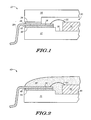
- FIG. 1 Shown in FIG. 1, in cross section, is a portion of a semiconductor device 10, in accordance with one embodiment of the invention, comprising a base 12 and an electronic component 14, such as an IC device, attached to a recessed bonding surface 16.
- a package lead 18 extends outwardly from electronic component 14 and is partially embedded in a first adhesive layer 20.
- Package lead 18 is connected to electronic component 14 by an device lead 22.
- a lid 24 covers electronic component 14 and is bonded to base 12 and portions of metal lead 18 by a second adhesive layer 26.
- First adhesive layer 20 and second adhesive layer 26 form a package seal 28.
- the union of lid 24 with base 12 forms a cavity 30 surrounding electronic component 14.
- package leads such as package lead 18, are numerous and extend outwardly from all four sides of the package.
- Package lead 18 is configured for surface mounting semiconductor device 10 onto a mounting substrate such as a printed circuit board.
- the package leads can be forged into other surface mounting compatible shapes such as a J-lead or a butt-joint configuration, or the like.
- the construction of package seal 28 begins with the formation of first adhesive layer 20.
- a solution containing a thermal epoxy material such as a novolak resin dissolved in a volatile organic solvent, is screened onto a lead mounting surface 32 at the perimeter of base 12.
- a thermoplastic resin material such as polyimide or polyimide-siloxane, or the like, can be used.
- Base 12 having first adhesive layer 20 in place, is then transferred to a furnace and heated to partially thermally cure first adhesive layer 20.
- a leadframe having a plurality of package leads, such as package lead 18, is clamped to base 12 bringing the package leads into intimate contact with first adhesive layer 20.
- the assembly is then placed in a furnace and heated at a temperature between about 125 to 175 degrees centigrade for about 1 to 2 hours.
- the heat cycle cures the epoxy by driving off solvents present in the screened epoxy mixture and cross-linking polymer chains in the epoxy.
- the clamping force partially embeds the leads in the epoxy compression bonding the leads in first adhesive layer 20.
- electronic component 14 is bonded to bonding surface 16 with a bonding material such as a polyimide or a filled bonding epoxy, or the like.
- Electronic component 14 is then electrically coupled to package lead 18 by forming device lead 22.
- Device lead 22 is one of many such leads used to connect electronic component 14 to the package leads of semiconductor device 10.
- Electronic component 14 can be one of several types of electronic devices such as an integrated circuit device, a discrete device or a hybrid device, or the like.
- device lead 22 can be a wire bond or a tape-automated-bond (TAB) bond.
- TAB tape-automated-bond
- electronic component 14 is mounted in a flip-chip configuration and bonded directly to the package leads.
- device lead 22 is depicted in the Figures as a wire bonded connection structure, it is intended that TAB and flip-chip methods of connection of electronic component 14 to package lead 18 be included within the scope of the invention.
- the construction of package seal 28 continues with the formation of second adhesive layer 26 using an epoxy material that can be cured at room temperature by exposure to UV frequency radiation.
- a UV-curable acrylated epoxy having a viscosity between about 20,000 to 60,000 centipoise, such as Westinghouse B-567 or B-5678-1 acrylated epoxy urethane compound, is screen printed onto a bonding portion 34 of lid 24.
- Lid 24 is then positioned onto base 12 and second adhesive layer 26 is brought into intimate contact with first adhesive layer 20 and package lead 18.
- lid 24 is constructed from a material that is opaque to UV radiation, such as alumina, aluminum nitride, copper, aluminum or brass, or the like.
- the outer edge of package seal 28 is then irradiated with about 340 to 360 millijoules per square centimeter of UV radiation at an intensity of about 290 to 310 watts per square centimeter for about 2 to 10 seconds.
- the exact radiation exposure conditions are dependant upon the particular epoxy chosen.
- the UV radiation is directed to each side of the QFP and initially impinges on an outer edge of package seal 28 as will be subsequently described in the discussion of the sealing process.
- the acrylated epoxy forming second adhesive layer 26 begins to cure, the polymer cross-linking process proceeds laterally toward cavity 30 until the entire seal area has been cured.
- the UV activated polymer cross-linking can continue to propagate laterally because as the epoxy cures it continues to transmit UV radiation.
- the UV radiation impinging on the outer edge of package seal 28 is not blocked by the previously cured epoxy on the outermost edge of package seal 28 and continues to laterally propagate through the acrylated epoxy.
- the characteristic of the cured acrylated epoxy to transmit UV radiation permits lid 24 to be clamped to base 14 prior to exposure to UV radiation.
- Semiconductor device 10 is then rotated so that all sides of the QFP package can be exposed to the UV radiation.
- lid 24 is constructed of a UV transparent material such as fused quartz, or unfilled or partially filled, polyphenylene sulfide plastic, or the like.
- a UV transparent material such as fused quartz, or unfilled or partially filled, polyphenylene sulfide plastic, or the like.
- the UV transparent nature of these materials allow the UV radiation to be directed to package seal 28 from a position directly above lid 24 on the opposite side of bonding portion 34.
- the use of a UV transparent material for the construction of lid 24 has the advantage of enabling the entire area of package seal 28 to be irradiated in a single operation.
- the QFP package can be sealed in one irradiation step thereby increasing the throughput of the sealing operation.
- FIG. 2 Shown in FIG. 2, in cross section, is a portion of a semiconductor device 40, in accordance with a further embodiment of the invention, comprising a base 41 having an IC device 42 attached to a recess surface portion 44.
- An adhesive layer 46 having a partially embedded package lead 50 therein, overlies a lead mount area 48.
- An inner lead 52 electrically couples IC device 42 with package lead 50.
- a body of UV-curable acrylated epoxy 54 overlies package lead 50 and covers inner lead 52 and IC device 42.
- Epoxy 54 forms a protective layer enclosing the environmentally sensitive elements of semiconductor device 40.
- a layer of UV-curable acrylated epoxy such as that previously described, is spread onto base 41.
- the thixotropic nature of epoxy material 54 causes the epoxy, when spread onto base 41, to flow in a conformal manner over base 41 such that the epoxy completely surrounds IC device 42 and inner lead 52.
- a protective seal is then formed upon exposure of epoxy material 54 to an amount of UV radiation sufficient to completely cure epoxy material 54.
- the QFP package type shown in FIG. 2 is illustrative of a standard surface mountable package; however, the invention is not intended to be so limited and other types of packages, both surface mountable and through-hole mountable packages can be used.
- lead 50 can be configured as a J-lead or a butt joint for surface mounting semiconductor device 40 to a mounting substrate.
- the present invention can be embodied in a standard dual-in-line package and package lead 50 configured for through-hole mounting of semiconductor device 40.
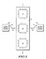
- FIG. 3 One embodiment of a room temperature package sealing process, according to the present invention, is schematically illustrated in FIG. 3.
- a number of semiconductor devices 10 having lid 24 screen printed with a UV-curable epoxy to a thickness of about 5 mill-inches and clamped to a base 12 are placed on a carrier tray 60.
- Carrier tray 60 is then placed on a moving belt (not shown) and transported between two UV-source units 62 and 64.
- the belt transporting carrier tray 60 and UV-source units 62 and 64 operate in an ambient environment having a temperature of about 20 to 40 degrees centigrade.
- the arrows shown in FIG. 3 indicate the direction of movement of carrier tray 60 relative to UV-source units 62 and 64.
- UV-sources units 62 and 64 are equipped with directional probes 66 and 68 connected to UV-source units 62 and 64 by fiber optic cables 70 and 72 respectively.
- UV-source units are capable of delivering 100 to 400 watts per square centimeter of UV radiation having a wavelength ranging from 320 to 380 nanometers.
- the flux of UV radiation emitted by directional probes 66 and 68 impinges on the outwardly exposed edge portion of the UV-curable epoxy.
- the amount of UV radiation necessary to perform the package seal process is dependant upon interrelated process parameters. For example, the amount of UV radiation necessary to seal a given package is dependent upon the particular type and thickness of UV-curable epoxy screen printed onto each lid of semiconductor devices 10. The linear speed the belt transporting carrier tray 60 is then adjusted to allow the necessary UV-radiation dose to be delivered to each of semiconductor devices 10.
- semiconductor devices 10 After initially transporting tray 60 past directional probes 66 and 68, the opposite sides of each of semiconductor devices 10 will have been sealed. At this point semiconductor devices 10 are rotated 90 degrees on carrier tray 60 and either again transported past UV-source units 62 and 68, or alternatively, transported past a second set UV radiation source units (not shown). It will be apparent to one skilled in the art that many variations of the process illustrated in FIG. 3 are possible. For example, semiconductor devices 10 can be vertically stacked in a rack and the rack can then be either raised or lowered through a UV-radiation field generated by four or more UV-source units, thus sealing the four sides of semiconductor devices 10 in one single UV exposure operation. Furthermore, a series of UV-reflective mirrors can be used to direct the UV-radiation from a single UV-source unit thereby exposing two or more sides of semiconductor devices 10 simultaneously.
- An advantage of the present invention is that the package is sealed at room temperature thus avoiding damage to temperature sensitive materials present in the electronic component housed within the package, and the oxidation of metals within the package.
- Package sealing processes of the prior art have been carried out at temperatures ranging from 400 to 500 degrees centigrade in the case of glass sealing, and 150 to 200 degrees in the case of thermal epoxy sealing. At these temperatures many metals such as those used to construct package leads 18 and 50 can oxidize. Oxidation of metals used to fabricate the package leads is undesirable because even a slight amount of oxidation can render the lead non-solder wettable compromising the ability to attach the semiconductor device to a mounting substrate such as a printed circuit board.
- oxide scales formed on the metal surface can flake off causing electrical shorting between adjacent device leads.
- the ability to seal the package at room temperature permits the use of certain metals having low electrical resistance for the construction of package leads 18 and 50. Metals such as copper, for example, could not be used in processes of the prior art because of the formation of oxide scales on the copper surface during package sealing.
- the ability to form a package seal at room temperature allows the use of copper package leads having a low electrical resistance. A semiconductor device having improved electrical performance that can be fabricated at a reduced cost is thus realized by the use of a UV-curable epoxy according to the present invention.
- a further advantage of the present invention relates to the ability to maintain the same air pressure in the cavity as the ambient during the formation of the package seal. Sealing the package at room temperature avoids a pressure build up in the cavity removing the driving force that would cause air to flow through the epoxy film as it is cured. A strong seal of uniform density is thus obtained that is free of voids or air pockets.
Abstract
Description
- This invention relates to semiconductor devices and more particularly to semiconductor devices having an electronic component sealed within a package.
- In the assembly of semiconductor devices, such as an integrated circuit (IC) device, or the like it is desirable to avoid exposing the devices to excessive heat that may cause damage to certain materials present in the device. Conventional materials and assembly processes used to form hermetic package seals often require high temperature process steps. For example, high temperature steps are often used to form a hermetic glass seal between the base and the lid of the package housing an electronic component. The glass sealing process is typically performed at temperatures ranging from about 400 to 500 degrees centigrade and heating times of about 1 to 2 hours. In this time and temperature range many glass materials begin to exhibit flow characteristics, which is necessary to form a glass seal, but the high temperature sealing process can also cause oxidation of many metals used to form package leads. For example, copper and aluminum must be plated with a non-readily oxidizable material such as nickel to prevent the formation of oxide scales on the lead surface. Additionally, the glass sealing process can cause cracking of the passivation layers overlying the circuit components of the IC device. Once the passivation layer has been compromised, the protection of the circuit elements against moisture and contamination has been lost and a potential for premature failure of the IC device exists.
- The need to produce more reliable semiconductor devices has led to the development of assembly processes using low temperature sealing materials. Both thermoplastic materials and thermosetting polymers, such as epoxy resins, have been developed for use as sealant materials to enclose an IC device within a package body. Thermal epoxies that can be cured at temperatures between 150 and 200 degrees centigrade have been developed. The thermal epoxy curing process initiates cross-linking of low-molecular-weight polymer chains forming high molecular weight interlinked polymer units.
- The use of epoxy sealant materials offers several advantages to semiconductor device manufactures and can be used for low temperature sealing of ceramic packages such as pin-grid-arrays (PGAs) and ceramic-quad-flat-packs (CQFPs). An low temperature epoxy sealant has potential to offer a highly reliable sealant in applications where a totally hermetic seal is not required. However, it has been observed that thermal epoxy materials can suffer defects during processing even at relatively moderate sealing temperatures.
- In an assembly process using a thermal epoxy, a layer of epoxy is screened onto a ceramic base then partially cured using a heat cycle of short duration to partially bond the epoxy to the lid. This step is known in the art as B-stage processing. A ceramic lid is then clamped onto the base and the assembly is heated to drive of solvents present in the epoxy and to form polymer cross-links in the epoxy film. Typically, the base and the lid are configured such that when they are brought together a cavity is formed in the interior of the package. The cured epoxy forms a seal between the lid and the base enclosing the IC device within the cavity. This process has the advantage of producing a seal at a lower temperature than that used to form a glass seal; however, the process is sensitive to pressure differentials between the cavity and the ambient environment. During the curing process, air trapped inside the cavity can expand and escape the confines of the cavity through the curing epoxy film. The air traversing the thermal epoxy film creates holes or voids in the epoxy resulting in the formation of a structurally weak seal that is prone to rupturing. A similar problem can be encountered if the assembly is cooled too rapidly after curing the epoxy. With rapid cooing the air pressure inside the cavity can momentarily drop below that of the outside ambient and air can flow into the cavity through the warm epoxy film forming voids in the film. The benefit of using a thermal epoxy as a seal material can thus be compromised by a pressure differential forcing air through the epoxy as the film is cured.
- The thermal epoxies overcome some of the problems of glass seals, but are themselves prone to seal integrity problems. Accordingly, a need existed for a semiconductor device having a package seal material capable of forming a seal at room temperature which overcomes the problems associated with high temperature glass seals and with epoxy seals, and a process for fabricating the same.
- An object of the invention is to provide an improved semiconductor device having a protective seal free from temperature and pressure induced defects.
- Another object of the invention is to provide an improved semiconductor device having a package sealed at room temperature.
- A further object of the invention is to provide a room temperature sealing process for the assembly of a semiconductor device.
- In accordance with a first aspect of the invention there is provided a semiconductor device comprising.
a base having an electronic component attached thereto;
an adhesive material overlying a lead mounting portion of the base;
a plurality of metal package leads partially embedded in the adhesive material extending outwardly from a position proximate the electronic component for electrically coupling the electronic component to a mounting substrate;
a plurality of device leads electrically connecting the electronic component to the plurality of package leads; and
closure means for covering the electronic component, the plurality of device leads and at least a portion of each of the plurality of package leads, the closure means including at least one UV-curable epoxy material,
whereby the closure means enables the semiconductor device to be sealed at room temperature. - In accordance with a second aspect of the invention there is provided a method for fabricating a semiconductor device comprising:
providing a base having an electronic component attached thereto;
screen printing a layer of UV-curable epoxy onto a bonding portion of a lid;
positioning the lid onto the base such that an area of UV-curable epoxy is outwardly exposed between the base and the lid; and
irradiating the outwardly exposed area with UV frequency radiation to cure the layer of UV-curable epoxysealing the lid to the base. - Preferably, the UV-curable epoxy material is a UV-curable thixotropic, acrylated epoxy.
- The package is sealed at room temperature by polymer cross-linking of the epoxy initiated by exposure of at least a portion of the epoxy to ultraviolet (UV) frequency radiation.
- It will be appreciated that an advantage of the present invention is that it can provide an improved semiconductor device having an oxide free copper leadframe, since the sealing process takes place at room temperature.
-
- FIG. 1 is a partial cross sectional view of a semiconductor device in accordance with one embodiment of the invention; and
- FIG. 2 is a partial cross sectional view of a semiconductor device in accordance with a further embodiment of the invention; and
- FIG. 3 schematically illustrates one embodiment of a package sealing process according to the invention.
- It will be appreciated that in FIGs. 1 and 2 the proportions of the various parts are not to scale. For example, the dimensions of some of the elements are exaggerated relative to each other for clarity.
- Shown in FIG. 1, in cross section, is a portion of a
semiconductor device 10, in accordance with one embodiment of the invention, comprising abase 12 and anelectronic component 14, such as an IC device, attached to a recessedbonding surface 16. Apackage lead 18 extends outwardly fromelectronic component 14 and is partially embedded in a firstadhesive layer 20.Package lead 18 is connected toelectronic component 14 by andevice lead 22. Alid 24 coverselectronic component 14 and is bonded tobase 12 and portions ofmetal lead 18 by a secondadhesive layer 26. Firstadhesive layer 20 and secondadhesive layer 26 form apackage seal 28. The union oflid 24 withbase 12 forms acavity 30 surroundingelectronic component 14. Those skilled in the art will recognize the package structure illustrated in FIG. 1 as having the configuration of a quad-flat-pack (QFP). In the standard QFP package design, package leads, such aspackage lead 18, are numerous and extend outwardly from all four sides of the package.Package lead 18 is configured for surfacemounting semiconductor device 10 onto a mounting substrate such as a printed circuit board. Alternatively, the package leads can be forged into other surface mounting compatible shapes such as a J-lead or a butt-joint configuration, or the like. - In accordance with one embodiment of the invention, the construction of
package seal 28 begins with the formation of firstadhesive layer 20. A solution containing a thermal epoxy material, such as a novolak resin dissolved in a volatile organic solvent, is screened onto alead mounting surface 32 at the perimeter ofbase 12. Alternatively, a thermoplastic resin material, such as polyimide or polyimide-siloxane, or the like, can be used.Base 12, having firstadhesive layer 20 in place, is then transferred to a furnace and heated to partially thermally cure firstadhesive layer 20. Following a cooling period, a leadframe having a plurality of package leads, such aspackage lead 18, is clamped to base 12 bringing the package leads into intimate contact with firstadhesive layer 20. The assembly is then placed in a furnace and heated at a temperature between about 125 to 175 degrees centigrade for about 1 to 2 hours. The heat cycle cures the epoxy by driving off solvents present in the screened epoxy mixture and cross-linking polymer chains in the epoxy. As the thermal epoxy approaches its glass transition temperature, the clamping force partially embeds the leads in the epoxy compression bonding the leads in firstadhesive layer 20. - After the package leads are partially embedded in first
adhesive layer 20,electronic component 14 is bonded tobonding surface 16 with a bonding material such as a polyimide or a filled bonding epoxy, or the like.Electronic component 14 is then electrically coupled to packagelead 18 by formingdevice lead 22.Device lead 22 is one of many such leads used to connectelectronic component 14 to the package leads ofsemiconductor device 10.Electronic component 14 can be one of several types of electronic devices such as an integrated circuit device, a discrete device or a hybrid device, or the like. In addition,device lead 22 can be a wire bond or a tape-automated-bond (TAB) bond. In another embodiment of the inventionelectronic component 14 is mounted in a flip-chip configuration and bonded directly to the package leads. Althoughdevice lead 22 is depicted in the Figures as a wire bonded connection structure, it is intended that TAB and flip-chip methods of connection ofelectronic component 14 to packagelead 18 be included within the scope of the invention. - According to the invention, the construction of
package seal 28 continues with the formation of secondadhesive layer 26 using an epoxy material that can be cured at room temperature by exposure to UV frequency radiation. A UV-curable acrylated epoxy, having a viscosity between about 20,000 to 60,000 centipoise, such as Westinghouse B-567 or B-5678-1 acrylated epoxy urethane compound, is screen printed onto abonding portion 34 oflid 24.Lid 24 is then positioned ontobase 12 and secondadhesive layer 26 is brought into intimate contact with firstadhesive layer 20 andpackage lead 18. In one embodiment of the invention,lid 24 is constructed from a material that is opaque to UV radiation, such as alumina, aluminum nitride, copper, aluminum or brass, or the like. The outer edge ofpackage seal 28 is then irradiated with about 340 to 360 millijoules per square centimeter of UV radiation at an intensity of about 290 to 310 watts per square centimeter for about 2 to 10 seconds. The exact radiation exposure conditions are dependant upon the particular epoxy chosen. The UV radiation is directed to each side of the QFP and initially impinges on an outer edge ofpackage seal 28 as will be subsequently described in the discussion of the sealing process. As the acrylated epoxy forming secondadhesive layer 26 begins to cure, the polymer cross-linking process proceeds laterally towardcavity 30 until the entire seal area has been cured. The UV activated polymer cross-linking can continue to propagate laterally because as the epoxy cures it continues to transmit UV radiation. Thus, the UV radiation impinging on the outer edge ofpackage seal 28 is not blocked by the previously cured epoxy on the outermost edge ofpackage seal 28 and continues to laterally propagate through the acrylated epoxy. The characteristic of the cured acrylated epoxy to transmit UV radiation permitslid 24 to be clamped tobase 14 prior to exposure to UV radiation.Semiconductor device 10 is then rotated so that all sides of the QFP package can be exposed to the UV radiation. - In another embodiment of the invention,
lid 24 is constructed of a UV transparent material such as fused quartz, or unfilled or partially filled, polyphenylene sulfide plastic, or the like. The UV transparent nature of these materials allow the UV radiation to be directed to packageseal 28 from a position directly abovelid 24 on the opposite side ofbonding portion 34. The use of a UV transparent material for the construction oflid 24 has the advantage of enabling the entire area ofpackage seal 28 to be irradiated in a single operation. In this embodiment of the invention the QFP package can be sealed in one irradiation step thereby increasing the throughput of the sealing operation. - One skilled in the art will recognize that other types of packages may be sealed using the UV-curable acrylated epoxy of the invention. Shown in FIG. 2, in cross section, is a portion of a
semiconductor device 40, in accordance with a further embodiment of the invention, comprising a base 41 having anIC device 42 attached to arecess surface portion 44. Anadhesive layer 46, having a partially embeddedpackage lead 50 therein, overlies alead mount area 48. Aninner lead 52 electricallycouples IC device 42 withpackage lead 50. A body of UV-curable acrylated epoxy 54overlies package lead 50 and coversinner lead 52 andIC device 42.Epoxy 54 forms a protective layer enclosing the environmentally sensitive elements ofsemiconductor device 40. In the process of assemblingsemiconductor device 40, afterlead 50 has been embedded inadhesive layer 46 andIC device 42 has been attached tobase 41, a layer of UV-curable acrylated epoxy, such as that previously described, is spread ontobase 41. The thixotropic nature ofepoxy material 54 causes the epoxy, when spread ontobase 41, to flow in a conformal manner overbase 41 such that the epoxy completely surroundsIC device 42 andinner lead 52. A protective seal is then formed upon exposure ofepoxy material 54 to an amount of UV radiation sufficient to completely cureepoxy material 54. - The QFP package type shown in FIG. 2 is illustrative of a standard surface mountable package; however, the invention is not intended to be so limited and other types of packages, both surface mountable and through-hole mountable packages can be used. For example, lead 50 can be configured as a J-lead or a butt joint for surface mounting
semiconductor device 40 to a mounting substrate. Furthermore, the present invention can be embodied in a standard dual-in-line package and package lead 50 configured for through-hole mounting ofsemiconductor device 40. - One embodiment of a room temperature package sealing process, according to the present invention, is schematically illustrated in FIG. 3. A number of
semiconductor devices 10 havinglid 24 screen printed with a UV-curable epoxy to a thickness of about 5 mill-inches and clamped to a base 12 are placed on acarrier tray 60.Carrier tray 60 is then placed on a moving belt (not shown) and transported between two UV-source units carrier tray 60 and UV-source units carrier tray 60 relative to UV-source units sources units directional probes source units fiber optic cables directional probes semiconductor devices 10. The linear speed the belt transportingcarrier tray 60 is then adjusted to allow the necessary UV-radiation dose to be delivered to each ofsemiconductor devices 10. - After initially transporting
tray 60 pastdirectional probes semiconductor devices 10 will have been sealed. At thispoint semiconductor devices 10 are rotated 90 degrees oncarrier tray 60 and either again transported past UV-source units semiconductor devices 10 can be vertically stacked in a rack and the rack can then be either raised or lowered through a UV-radiation field generated by four or more UV-source units, thus sealing the four sides ofsemiconductor devices 10 in one single UV exposure operation. Furthermore, a series of UV-reflective mirrors can be used to direct the UV-radiation from a single UV-source unit thereby exposing two or more sides ofsemiconductor devices 10 simultaneously. - An advantage of the present invention is that the package is sealed at room temperature thus avoiding damage to temperature sensitive materials present in the electronic component housed within the package, and the oxidation of metals within the package. Package sealing processes of the prior art have been carried out at temperatures ranging from 400 to 500 degrees centigrade in the case of glass sealing, and 150 to 200 degrees in the case of thermal epoxy sealing. At these temperatures many metals such as those used to construct package leads 18 and 50 can oxidize. Oxidation of metals used to fabricate the package leads is undesirable because even a slight amount of oxidation can render the lead non-solder wettable compromising the ability to attach the semiconductor device to a mounting substrate such as a printed circuit board. Furthermore, oxide scales formed on the metal surface can flake off causing electrical shorting between adjacent device leads. The ability to seal the package at room temperature, as provided by the present invention, permits the use of certain metals having low electrical resistance for the construction of package leads 18 and 50. Metals such as copper, for example, could not be used in processes of the prior art because of the formation of oxide scales on the copper surface during package sealing. The ability to form a package seal at room temperature, provided by the present invention, allows the use of copper package leads having a low electrical resistance. A semiconductor device having improved electrical performance that can be fabricated at a reduced cost is thus realized by the use of a UV-curable epoxy according to the present invention.
- A further advantage of the present invention relates to the ability to maintain the same air pressure in the cavity as the ambient during the formation of the package seal. Sealing the package at room temperature avoids a pressure build up in the cavity removing the driving force that would cause air to flow through the epoxy film as it is cured. A strong seal of uniform density is thus obtained that is free of voids or air pockets.
- Thus it is apparent that there has been provided, in accordance with the invention, a semiconductor device and process which fully meets the objects and advantages set forth above. Although particular embodiments of the invention have been described in the foregoing description, it will be apparent to one skilled in the art that numerous modifications and variations can be made to the presented embodiments which still fall within the spirit and scope of the invention. For example, the invention can be applied to semiconductor devices lacking outwardly extending exterior leads such as a leadless-chip-carrier (LCC) or and other types of ceramic packages such as a PGA or a ceramic dual-in-line package (DIP). Accordingly, it is intended that all such variations and modifications as fall within the scope of the appended claims and equivalents thereof be included within the invention.
Claims (8)
- A semiconductor device (10) comprising:
a base (12) having an electronic component (14) attached thereto;
an adhesive material (20) overlying a lead mounting portion (32) of the base (12);
a plurality of metal package leads (18) partially embedded in the adhesive material (20) extending outwardly from a position proximate the electronic component (14) for electrically coupling the electronic component (14) to a mounting substrate;
a plurality of device leads (22) electrically connecting the electronic component (14) to the plurality of package leads (18); and
closure means (24) for covering the electronic component (14), the plurality of device leads (22) and at least a portion of each of the plurality of package leads (18), the closure means (24) including at least one UV-curable epoxy material (26), whereby the closure means (24) enables the semiconductor device (10) to be sealed at room temperature. - The semiconductor device of claim 1 wherein the closure means (24) comprises a lid (24) bonded to the base (12) by the UV-curable epoxy material (26).
- The semiconductor device (10) of claim 2 wherein the lid (24) is constructed from a UV transmitting material.
- The semiconductor device (10) of claim 2 wherein the lid (24) is constructed from a material selected from the group consisting of alumina, aluminum nitride, aluminum, copper and brass.
- The semiconductor device (10) of claim 1 wherein the closure means comprises a body of UV-curable epoxy material (26) disposed on the base (12) forming a protective seal enclosing the electronic component (14) and at least a portion of each of the plurality of package leads (18).
- A method for fabricating a semiconductor device (10) comprising:
providing a base (12) having an electronic component (14) attached thereto;
screen printing a layer of UV-curable epoxy (26) onto a bonding portion (26) of a lid (24);
positioning the lid (24) onto the base (12) such that an area of UV-curable epoxy is outwardly exposed between the base (12) and the lid (24); and
irradiating the outwardly exposed area with UV frequency radiation to cure the layer of UV-curable epoxy (26) sealing the lid (24) to the base (12). - The method of claim 6 wherein said irradiating comprises directing a beam of UV radiation having a wavelength of about 320 to 380 nm to the outwardly exposed edge area.
- The method of claim 6 wherein the step of irradiating comprises passing the outwardly exposed area of UV-curable epoxy through a UV radiation field in a continuous linear operation.
Applications Claiming Priority (2)
| Application Number | Priority Date | Filing Date | Title |
|---|---|---|---|
| US498156 | 1990-03-23 | ||
| US07/498,156 US5117279A (en) | 1990-03-23 | 1990-03-23 | Semiconductor device having a low temperature uv-cured epoxy seal |
Publications (3)
| Publication Number | Publication Date |
|---|---|
| EP0447884A2 true EP0447884A2 (en) | 1991-09-25 |
| EP0447884A3 EP0447884A3 (en) | 1994-02-23 |
| EP0447884B1 EP0447884B1 (en) | 1998-07-01 |
Family
ID=23979815
Family Applications (1)
| Application Number | Title | Priority Date | Filing Date |
|---|---|---|---|
| EP91103481A Expired - Lifetime EP0447884B1 (en) | 1990-03-23 | 1991-03-07 | Method for making a semiconductor device having a low temperature UV-cured epoxy seal |
Country Status (4)
| Country | Link |
|---|---|
| US (1) | US5117279A (en) |
| EP (1) | EP0447884B1 (en) |
| JP (1) | JP3010784B2 (en) |
| DE (1) | DE69129668T2 (en) |
Cited By (9)
| Publication number | Priority date | Publication date | Assignee | Title |
|---|---|---|---|---|
| EP0637839A2 (en) * | 1993-08-03 | 1995-02-08 | International Business Machines Corporation | Chip carrier with protective coating for circuitized surface |
| EP0673547A1 (en) * | 1992-12-09 | 1995-09-27 | Olin Corporation | Electronic package sealed with a dispensable adhesive |
| WO1996007204A1 (en) * | 1994-08-26 | 1996-03-07 | National Semiconductor Corporation | Ultra-thin composite package for integrated circuits |
| EP0862790A1 (en) * | 1996-09-20 | 1998-09-09 | Motorola, Inc. | Electronic control module having fluid-tight seals |
| EP1251557A2 (en) * | 1994-07-26 | 2002-10-23 | Koninklijke Philips Electronics N.V. | Method of manufacturing semiconductor devices and semiconductor device |
| WO2005091359A1 (en) * | 2004-03-20 | 2005-09-29 | Robert Bosch Gmbh | Method for producing a sensor module and corresponding sensor module |
| EP1619726A1 (en) * | 2004-07-22 | 2006-01-25 | St Microelectronics S.A. | Package for optical semiconductor detector |
| US7127362B2 (en) | 2000-08-22 | 2006-10-24 | Mundt Randall S | Process tolerant methods and apparatus for obtaining data |
| EP2019424A3 (en) * | 2007-07-26 | 2009-12-30 | SEMIKRON Elektronik GmbH & Co. KG | High performance semiconductor module with sealant device on substrate carrier and corresponding production method |
Families Citing this family (29)
| Publication number | Priority date | Publication date | Assignee | Title |
|---|---|---|---|---|
| TW332348B (en) * | 1992-06-23 | 1998-05-21 | Sony Co Ltd | Manufacturing method for solid state motion picture device provides a highly accurate and low cost solid state motion picture device by use of empty package made of resin. |
| US5477008A (en) * | 1993-03-19 | 1995-12-19 | Olin Corporation | Polymer plug for electronic packages |
| JPH0837252A (en) * | 1994-07-22 | 1996-02-06 | Nec Corp | Semiconductor device |
| WO1996034517A1 (en) * | 1995-04-26 | 1996-10-31 | Buztronics, Inc. | Electronic novelty assembly including a pin switch and embedded printed circuit component |
| US7041771B1 (en) | 1995-08-11 | 2006-05-09 | Kac Holdings, Inc. | Encapsulant with fluxing properties and method of use in flip-chip surface mount reflow soldering |
| US5938956A (en) * | 1996-09-10 | 1999-08-17 | Micron Technology, Inc. | Circuit and method for heating an adhesive to package or rework a semiconductor die |
| US6426484B1 (en) | 1996-09-10 | 2002-07-30 | Micron Technology, Inc. | Circuit and method for heating an adhesive to package or rework a semiconductor die |
| US6274927B1 (en) * | 1999-06-03 | 2001-08-14 | Amkor Technology, Inc. | Plastic package for an optical integrated circuit device and method of making |
| US6432752B1 (en) * | 2000-08-17 | 2002-08-13 | Micron Technology, Inc. | Stereolithographic methods for fabricating hermetic semiconductor device packages and semiconductor devices including stereolithographically fabricated hermetic packages |
| JP4003860B2 (en) * | 2000-11-02 | 2007-11-07 | 富士通株式会社 | Microactuator and manufacturing method thereof |
| US6376266B1 (en) * | 2000-11-06 | 2002-04-23 | Semiconductor Components Industries Llc | Semiconductor package and method for forming same |
| US6747298B2 (en) * | 2001-07-23 | 2004-06-08 | Cree, Inc. | Collets for bonding of light emitting diodes having shaped substrates |
| US6888167B2 (en) | 2001-07-23 | 2005-05-03 | Cree, Inc. | Flip-chip bonding of light emitting devices and light emitting devices suitable for flip-chip bonding |
| US6692610B2 (en) * | 2001-07-26 | 2004-02-17 | Osram Opto Semiconductors Gmbh | Oled packaging |
| US6861720B1 (en) | 2001-08-29 | 2005-03-01 | Amkor Technology, Inc. | Placement template and method for placing optical dies |
| US6759266B1 (en) * | 2001-09-04 | 2004-07-06 | Amkor Technology, Inc. | Quick sealing glass-lidded package fabrication method |
| US20030054583A1 (en) * | 2001-09-20 | 2003-03-20 | Eastman Kodak Company | Method for producing an image sensor assembly |
| US7276394B2 (en) * | 2001-09-20 | 2007-10-02 | Eastman Kodak Company | Large area flat image sensor assembly |
| US6507097B1 (en) * | 2001-11-29 | 2003-01-14 | Clarisay, Inc. | Hermetic package for pyroelectric-sensitive electronic device and method of manufacturing the same |
| US6784534B1 (en) | 2002-02-06 | 2004-08-31 | Amkor Technology, Inc. | Thin integrated circuit package having an optically transparent window |
| JP3560161B1 (en) * | 2003-01-30 | 2004-09-02 | 日立化成工業株式会社 | Method for producing epoxy resin composition for semiconductor encapsulation |
| US7195953B2 (en) * | 2003-04-02 | 2007-03-27 | Yamaha Corporation | Method of manufacturing a semiconductor package using a lead frame having through holes or hollows therein |
| US7517728B2 (en) * | 2004-03-31 | 2009-04-14 | Cree, Inc. | Semiconductor light emitting devices including a luminescent conversion element |
| KR100782798B1 (en) * | 2006-02-22 | 2007-12-05 | 삼성전기주식회사 | COB Package and Its Manufacturing method |
| DE102006008793A1 (en) * | 2006-02-24 | 2007-09-13 | Osram Opto Semiconductors Gmbh | Electronic component |
| US8421214B2 (en) * | 2007-10-10 | 2013-04-16 | Vishay General Semiconductor Llc | Semiconductor device and method for manufacturing a semiconductor device |
| US9147813B2 (en) | 2011-09-09 | 2015-09-29 | Avago Technologies General Ip (Singapore) Pte. Ltd. | High thermal conductivity and low degradation die attach with dual adhesive |
| US9907177B2 (en) | 2013-12-19 | 2018-02-27 | Daishinku Corporation | Electronic component-use package and piezoelectric device |
| US10170304B1 (en) | 2017-10-25 | 2019-01-01 | Globalfoundries Inc. | Self-aligned nanotube structures |
Citations (6)
| Publication number | Priority date | Publication date | Assignee | Title |
|---|---|---|---|---|
| US4000054A (en) * | 1970-11-06 | 1976-12-28 | Microsystems International Limited | Method of making thin film crossover structure |
| US4141055A (en) * | 1977-04-27 | 1979-02-20 | Bell Telephone Laboratories, Incorporated | Crossover structure for microelectronic circuits |
| EP0114258A1 (en) * | 1982-11-30 | 1984-08-01 | Kabushiki Kaisha Toshiba | Resin encapsulation type photo-semiconductor devices |
| US4524238A (en) * | 1982-12-29 | 1985-06-18 | Olin Corporation | Semiconductor packages |
| US4703338A (en) * | 1983-10-14 | 1987-10-27 | Daicel Chemical Industries, Ltd. | Resin composition to seal electronic device |
| US4783697A (en) * | 1985-01-07 | 1988-11-08 | Motorola, Inc. | Leadless chip carrier for RF power transistors or the like |
Family Cites Families (1)
| Publication number | Priority date | Publication date | Assignee | Title |
|---|---|---|---|---|
| US4480009A (en) * | 1980-12-15 | 1984-10-30 | M&T Chemicals Inc. | Siloxane-containing polymers |
-
1990
- 1990-03-23 US US07/498,156 patent/US5117279A/en not_active Expired - Fee Related
-
1991
- 1991-03-07 EP EP91103481A patent/EP0447884B1/en not_active Expired - Lifetime
- 1991-03-07 DE DE69129668T patent/DE69129668T2/en not_active Expired - Fee Related
- 1991-03-22 JP JP3130804A patent/JP3010784B2/en not_active Expired - Fee Related
Patent Citations (6)
| Publication number | Priority date | Publication date | Assignee | Title |
|---|---|---|---|---|
| US4000054A (en) * | 1970-11-06 | 1976-12-28 | Microsystems International Limited | Method of making thin film crossover structure |
| US4141055A (en) * | 1977-04-27 | 1979-02-20 | Bell Telephone Laboratories, Incorporated | Crossover structure for microelectronic circuits |
| EP0114258A1 (en) * | 1982-11-30 | 1984-08-01 | Kabushiki Kaisha Toshiba | Resin encapsulation type photo-semiconductor devices |
| US4524238A (en) * | 1982-12-29 | 1985-06-18 | Olin Corporation | Semiconductor packages |
| US4703338A (en) * | 1983-10-14 | 1987-10-27 | Daicel Chemical Industries, Ltd. | Resin composition to seal electronic device |
| US4783697A (en) * | 1985-01-07 | 1988-11-08 | Motorola, Inc. | Leadless chip carrier for RF power transistors or the like |
Non-Patent Citations (1)
| Title |
|---|
| PATENT ABSTRACTS OF JAPAN vol. 12 no. 369 (E-665) Oct. 4, 1988; & JP-A-63-122249 * |
Cited By (16)
| Publication number | Priority date | Publication date | Assignee | Title |
|---|---|---|---|---|
| EP0673547A1 (en) * | 1992-12-09 | 1995-09-27 | Olin Corporation | Electronic package sealed with a dispensable adhesive |
| EP0673547A4 (en) * | 1992-12-09 | 1996-03-13 | Olin Corp | Electronic package sealed with a dispensable adhesive. |
| CN1051402C (en) * | 1993-08-03 | 2000-04-12 | 国际商业机器公司 | Chip carrier with protective coating for circuitized surface |
| EP0637839A3 (en) * | 1993-08-03 | 1995-06-28 | Ibm | Chip carrier with protective coating for circuitized surface. |
| EP0637839A2 (en) * | 1993-08-03 | 1995-02-08 | International Business Machines Corporation | Chip carrier with protective coating for circuitized surface |
| EP1251557A3 (en) * | 1994-07-26 | 2003-04-09 | Koninklijke Philips Electronics N.V. | Method of manufacturing semiconductor devices and semiconductor device |
| EP1251557A2 (en) * | 1994-07-26 | 2002-10-23 | Koninklijke Philips Electronics N.V. | Method of manufacturing semiconductor devices and semiconductor device |
| US6184575B1 (en) | 1994-08-26 | 2001-02-06 | National Semiconductor Corporation | Ultra-thin composite package for integrated circuits |
| WO1996007204A1 (en) * | 1994-08-26 | 1996-03-07 | National Semiconductor Corporation | Ultra-thin composite package for integrated circuits |
| EP0862790A4 (en) * | 1996-09-20 | 1999-08-04 | Motorola Inc | Electronic control module having fluid-tight seals |
| EP0862790A1 (en) * | 1996-09-20 | 1998-09-09 | Motorola, Inc. | Electronic control module having fluid-tight seals |
| US7127362B2 (en) | 2000-08-22 | 2006-10-24 | Mundt Randall S | Process tolerant methods and apparatus for obtaining data |
| WO2005091359A1 (en) * | 2004-03-20 | 2005-09-29 | Robert Bosch Gmbh | Method for producing a sensor module and corresponding sensor module |
| EP1619726A1 (en) * | 2004-07-22 | 2006-01-25 | St Microelectronics S.A. | Package for optical semiconductor detector |
| EP2019424A3 (en) * | 2007-07-26 | 2009-12-30 | SEMIKRON Elektronik GmbH & Co. KG | High performance semiconductor module with sealant device on substrate carrier and corresponding production method |
| US8053884B2 (en) | 2007-07-26 | 2011-11-08 | Semikron Elektronik Gmbh & Co. Kg | Power semiconductor module with sealing device for sealing to a substrate carrier and method for manufacturing it |
Also Published As
| Publication number | Publication date |
|---|---|
| EP0447884A3 (en) | 1994-02-23 |
| JPH0621251A (en) | 1994-01-28 |
| DE69129668T2 (en) | 1999-03-11 |
| EP0447884B1 (en) | 1998-07-01 |
| US5117279A (en) | 1992-05-26 |
| JP3010784B2 (en) | 2000-02-21 |
| DE69129668D1 (en) | 1998-08-06 |
Similar Documents
| Publication | Publication Date | Title |
|---|---|---|
| US5117279A (en) | Semiconductor device having a low temperature uv-cured epoxy seal | |
| US6432253B1 (en) | Cover with adhesive preform and method for applying same | |
| JP3692935B2 (en) | Manufacturing method of semiconductor device | |
| US6428650B1 (en) | Cover for an optical device and method for making same | |
| US4480262A (en) | Semiconductor casing | |
| JP4362366B2 (en) | Method for forming air cavity package of semiconductor circuit element | |
| US5650593A (en) | Thermally enhanced chip carrier package | |
| EP0421579B1 (en) | Plastic encapsulated integrated circuit die packages and method of making same | |
| US5458716A (en) | Methods for manufacturing a thermally enhanced molded cavity package having a parallel lid | |
| US6409859B1 (en) | Method of making a laminated adhesive lid, as for an Electronic device | |
| KR100336329B1 (en) | Manufacturing method of semiconductor device | |
| US20040108588A1 (en) | Package for microchips | |
| JPH08274204A (en) | Hermetic seal system and hermetic seal method for device | |
| JP2006121861A (en) | Power converter | |
| US5567984A (en) | Process for fabricating an electronic circuit package | |
| JP3414755B2 (en) | System and method for curing liquid resin encapsulants of microelectronic components with microwave energy | |
| EP1503412A2 (en) | Semiconductor device and manufacturing method of the same | |
| JP4288517B2 (en) | Manufacturing method of semiconductor device | |
| MXPA98008326A (en) | Solidification with microwave energy of liquid resin encapsulants for microelectron components | |
| EP0892986A1 (en) | Curing liquid resin encapsulants of microelectronics components with microwave energy | |
| JP4583086B2 (en) | Optical semiconductor device | |
| JPS6215840A (en) | Chip carrier for electronic element | |
| JP2005252310A (en) | Semiconductor device and its manufacturing method, circuit board, and electronic apparatus | |
| KR20000005272A (en) | Curable liquid resin encapsulants of microelectronics components with microwave energy | |
| JPH0220032A (en) | Sealing method for resin of semiconductor element |
Legal Events
| Date | Code | Title | Description |
|---|---|---|---|
| PUAI | Public reference made under article 153(3) epc to a published international application that has entered the european phase |
Free format text: ORIGINAL CODE: 0009012 |
|
| AK | Designated contracting states |
Kind code of ref document: A2 Designated state(s): DE FR GB IT |
|
| PUAL | Search report despatched |
Free format text: ORIGINAL CODE: 0009013 |
|
| AK | Designated contracting states |
Kind code of ref document: A3 Designated state(s): DE FR GB IT |
|
| 17P | Request for examination filed |
Effective date: 19940818 |
|
| 17Q | First examination report despatched |
Effective date: 19951124 |
|
| GRAG | Despatch of communication of intention to grant |
Free format text: ORIGINAL CODE: EPIDOS AGRA |
|
| GRAG | Despatch of communication of intention to grant |
Free format text: ORIGINAL CODE: EPIDOS AGRA |
|
| GRAH | Despatch of communication of intention to grant a patent |
Free format text: ORIGINAL CODE: EPIDOS IGRA |
|
| GRAH | Despatch of communication of intention to grant a patent |
Free format text: ORIGINAL CODE: EPIDOS IGRA |
|
| GRAA | (expected) grant |
Free format text: ORIGINAL CODE: 0009210 |
|
| ITF | It: translation for a ep patent filed |
Owner name: BARZANO' E ZANARDO ROMA S.P.A. |
|
| AK | Designated contracting states |
Kind code of ref document: B1 Designated state(s): DE FR GB IT |
|
| REF | Corresponds to: |
Ref document number: 69129668 Country of ref document: DE Date of ref document: 19980806 |
|
| ET | Fr: translation filed | ||
| PG25 | Lapsed in a contracting state [announced via postgrant information from national office to epo] |
Ref country code: GB Free format text: LAPSE BECAUSE OF NON-PAYMENT OF DUE FEES Effective date: 19990307 |
|
| PLBE | No opposition filed within time limit |
Free format text: ORIGINAL CODE: 0009261 |
|
| STAA | Information on the status of an ep patent application or granted ep patent |
Free format text: STATUS: NO OPPOSITION FILED WITHIN TIME LIMIT |
|
| 26N | No opposition filed | ||
| GBPC | Gb: european patent ceased through non-payment of renewal fee |
Effective date: 19990307 |
|
| PG25 | Lapsed in a contracting state [announced via postgrant information from national office to epo] |
Ref country code: FR Free format text: LAPSE BECAUSE OF NON-PAYMENT OF DUE FEES Effective date: 19991130 |
|
| REG | Reference to a national code |
Ref country code: FR Ref legal event code: ST |
|
| PG25 | Lapsed in a contracting state [announced via postgrant information from national office to epo] |
Ref country code: DE Free format text: LAPSE BECAUSE OF NON-PAYMENT OF DUE FEES Effective date: 20000101 |
|
| PG25 | Lapsed in a contracting state [announced via postgrant information from national office to epo] |
Ref country code: IT Free format text: LAPSE BECAUSE OF NON-PAYMENT OF DUE FEES;WARNING: LAPSES OF ITALIAN PATENTS WITH EFFECTIVE DATE BEFORE 2007 MAY HAVE OCCURRED AT ANY TIME BEFORE 2007. THE CORRECT EFFECTIVE DATE MAY BE DIFFERENT FROM THE ONE RECORDED. Effective date: 20050307 |