EP0452054A1 - HEMT structure with passivated structure - Google Patents
HEMT structure with passivated structure Download PDFInfo
- Publication number
- EP0452054A1 EP0452054A1 EP91303050A EP91303050A EP0452054A1 EP 0452054 A1 EP0452054 A1 EP 0452054A1 EP 91303050 A EP91303050 A EP 91303050A EP 91303050 A EP91303050 A EP 91303050A EP 0452054 A1 EP0452054 A1 EP 0452054A1
- Authority
- EP
- European Patent Office
- Prior art keywords
- layer
- schottky
- gate
- donor
- semiconductive material
- Prior art date
- Legal status (The legal status is an assumption and is not a legal conclusion. Google has not performed a legal analysis and makes no representation as to the accuracy of the status listed.)
- Granted
Links
- 239000000463 material Substances 0.000 claims abstract description 29
- 239000000758 substrate Substances 0.000 claims abstract description 8
- 229910000530 Gallium indium arsenide Inorganic materials 0.000 claims description 8
- 230000005669 field effect Effects 0.000 claims description 5
- 229910000980 Aluminium gallium arsenide Inorganic materials 0.000 claims 1
- 239000004065 semiconductor Substances 0.000 claims 1
- 238000002161 passivation Methods 0.000 abstract description 11
- 229910052782 aluminium Inorganic materials 0.000 abstract description 4
- XAGFODPZIPBFFR-UHFFFAOYSA-N aluminium Chemical compound [Al] XAGFODPZIPBFFR-UHFFFAOYSA-N 0.000 abstract description 4
- 230000003647 oxidation Effects 0.000 description 9
- 238000007254 oxidation reaction Methods 0.000 description 9
- 238000005530 etching Methods 0.000 description 6
- 125000006850 spacer group Chemical group 0.000 description 6
- JBRZTFJDHDCESZ-UHFFFAOYSA-N AsGa Chemical compound [As]#[Ga] JBRZTFJDHDCESZ-UHFFFAOYSA-N 0.000 description 4
- FTWRSWRBSVXQPI-UHFFFAOYSA-N alumanylidynearsane;gallanylidynearsane Chemical compound [As]#[Al].[As]#[Ga] FTWRSWRBSVXQPI-UHFFFAOYSA-N 0.000 description 4
- 230000004888 barrier function Effects 0.000 description 4
- 229910001218 Gallium arsenide Inorganic materials 0.000 description 3
- 229910000673 Indium arsenide Inorganic materials 0.000 description 1
- 229910052581 Si3N4 Inorganic materials 0.000 description 1
- VYPSYNLAJGMNEJ-UHFFFAOYSA-N Silicium dioxide Chemical compound O=[Si]=O VYPSYNLAJGMNEJ-UHFFFAOYSA-N 0.000 description 1
- 230000002411 adverse Effects 0.000 description 1
- AJGDITRVXRPLBY-UHFFFAOYSA-N aluminum indium Chemical compound [Al].[In] AJGDITRVXRPLBY-UHFFFAOYSA-N 0.000 description 1
- 230000015556 catabolic process Effects 0.000 description 1
- 238000006731 degradation reaction Methods 0.000 description 1
- 230000000694 effects Effects 0.000 description 1
- 238000000034 method Methods 0.000 description 1
- 230000004048 modification Effects 0.000 description 1
- 238000012986 modification Methods 0.000 description 1
- 230000001590 oxidative effect Effects 0.000 description 1
- 230000001902 propagating effect Effects 0.000 description 1
- 230000009467 reduction Effects 0.000 description 1
- 230000004044 response Effects 0.000 description 1
- 229910052710 silicon Inorganic materials 0.000 description 1
- 239000010703 silicon Substances 0.000 description 1
- HQVNEWCFYHHQES-UHFFFAOYSA-N silicon nitride Chemical compound N12[Si]34N5[Si]62N3[Si]51N64 HQVNEWCFYHHQES-UHFFFAOYSA-N 0.000 description 1
- 229910052814 silicon oxide Inorganic materials 0.000 description 1
- 230000007480 spreading Effects 0.000 description 1
Images

Classifications
-
- H—ELECTRICITY
- H01—ELECTRIC ELEMENTS
- H01L—SEMICONDUCTOR DEVICES NOT COVERED BY CLASS H10
- H01L29/00—Semiconductor devices adapted for rectifying, amplifying, oscillating or switching, or capacitors or resistors with at least one potential-jump barrier or surface barrier, e.g. PN junction depletion layer or carrier concentration layer; Details of semiconductor bodies or of electrodes thereof ; Multistep manufacturing processes therefor
- H01L29/02—Semiconductor bodies ; Multistep manufacturing processes therefor
- H01L29/12—Semiconductor bodies ; Multistep manufacturing processes therefor characterised by the materials of which they are formed
- H01L29/20—Semiconductor bodies ; Multistep manufacturing processes therefor characterised by the materials of which they are formed including, apart from doping materials or other impurities, only AIIIBV compounds
- H01L29/201—Semiconductor bodies ; Multistep manufacturing processes therefor characterised by the materials of which they are formed including, apart from doping materials or other impurities, only AIIIBV compounds including two or more compounds, e.g. alloys
- H01L29/205—Semiconductor bodies ; Multistep manufacturing processes therefor characterised by the materials of which they are formed including, apart from doping materials or other impurities, only AIIIBV compounds including two or more compounds, e.g. alloys in different semiconductor regions, e.g. heterojunctions
-
- H—ELECTRICITY
- H01—ELECTRIC ELEMENTS
- H01L—SEMICONDUCTOR DEVICES NOT COVERED BY CLASS H10
- H01L23/00—Details of semiconductor or other solid state devices
- H01L23/28—Encapsulations, e.g. encapsulating layers, coatings, e.g. for protection
- H01L23/29—Encapsulations, e.g. encapsulating layers, coatings, e.g. for protection characterised by the material, e.g. carbon
- H01L23/291—Oxides or nitrides or carbides, e.g. ceramics, glass
-
- H—ELECTRICITY
- H01—ELECTRIC ELEMENTS
- H01L—SEMICONDUCTOR DEVICES NOT COVERED BY CLASS H10
- H01L29/00—Semiconductor devices adapted for rectifying, amplifying, oscillating or switching, or capacitors or resistors with at least one potential-jump barrier or surface barrier, e.g. PN junction depletion layer or carrier concentration layer; Details of semiconductor bodies or of electrodes thereof ; Multistep manufacturing processes therefor
- H01L29/02—Semiconductor bodies ; Multistep manufacturing processes therefor
- H01L29/12—Semiconductor bodies ; Multistep manufacturing processes therefor characterised by the materials of which they are formed
- H01L29/15—Structures with periodic or quasi periodic potential variation, e.g. multiple quantum wells, superlattices
- H01L29/151—Compositional structures
- H01L29/152—Compositional structures with quantum effects only in vertical direction, i.e. layered structures with quantum effects solely resulting from vertical potential variation
- H01L29/155—Comprising only semiconductor materials
-
- H—ELECTRICITY
- H01—ELECTRIC ELEMENTS
- H01L—SEMICONDUCTOR DEVICES NOT COVERED BY CLASS H10
- H01L29/00—Semiconductor devices adapted for rectifying, amplifying, oscillating or switching, or capacitors or resistors with at least one potential-jump barrier or surface barrier, e.g. PN junction depletion layer or carrier concentration layer; Details of semiconductor bodies or of electrodes thereof ; Multistep manufacturing processes therefor
- H01L29/66—Types of semiconductor device ; Multistep manufacturing processes therefor
- H01L29/68—Types of semiconductor device ; Multistep manufacturing processes therefor controllable by only the electric current supplied, or only the electric potential applied, to an electrode which does not carry the current to be rectified, amplified or switched
- H01L29/76—Unipolar devices, e.g. field effect transistors
- H01L29/772—Field effect transistors
- H01L29/778—Field effect transistors with two-dimensional charge carrier gas channel, e.g. HEMT ; with two-dimensional charge-carrier layer formed at a heterojunction interface
- H01L29/7782—Field effect transistors with two-dimensional charge carrier gas channel, e.g. HEMT ; with two-dimensional charge-carrier layer formed at a heterojunction interface with confinement of carriers by at least two heterojunctions, e.g. DHHEMT, quantum well HEMT, DHMODFET
- H01L29/7783—Field effect transistors with two-dimensional charge carrier gas channel, e.g. HEMT ; with two-dimensional charge-carrier layer formed at a heterojunction interface with confinement of carriers by at least two heterojunctions, e.g. DHHEMT, quantum well HEMT, DHMODFET using III-V semiconductor material
-
- H—ELECTRICITY
- H01—ELECTRIC ELEMENTS
- H01L—SEMICONDUCTOR DEVICES NOT COVERED BY CLASS H10
- H01L29/00—Semiconductor devices adapted for rectifying, amplifying, oscillating or switching, or capacitors or resistors with at least one potential-jump barrier or surface barrier, e.g. PN junction depletion layer or carrier concentration layer; Details of semiconductor bodies or of electrodes thereof ; Multistep manufacturing processes therefor
- H01L29/66—Types of semiconductor device ; Multistep manufacturing processes therefor
- H01L29/68—Types of semiconductor device ; Multistep manufacturing processes therefor controllable by only the electric current supplied, or only the electric potential applied, to an electrode which does not carry the current to be rectified, amplified or switched
- H01L29/76—Unipolar devices, e.g. field effect transistors
- H01L29/772—Field effect transistors
- H01L29/778—Field effect transistors with two-dimensional charge carrier gas channel, e.g. HEMT ; with two-dimensional charge-carrier layer formed at a heterojunction interface
- H01L29/7786—Field effect transistors with two-dimensional charge carrier gas channel, e.g. HEMT ; with two-dimensional charge-carrier layer formed at a heterojunction interface with direct single heterostructure, i.e. with wide bandgap layer formed on top of active layer, e.g. direct single heterostructure MIS-like HEMT
- H01L29/7787—Field effect transistors with two-dimensional charge carrier gas channel, e.g. HEMT ; with two-dimensional charge-carrier layer formed at a heterojunction interface with direct single heterostructure, i.e. with wide bandgap layer formed on top of active layer, e.g. direct single heterostructure MIS-like HEMT with wide bandgap charge-carrier supplying layer, e.g. direct single heterostructure MODFET
-
- H—ELECTRICITY
- H01—ELECTRIC ELEMENTS
- H01L—SEMICONDUCTOR DEVICES NOT COVERED BY CLASS H10
- H01L2924/00—Indexing scheme for arrangements or methods for connecting or disconnecting semiconductor or solid-state bodies as covered by H01L24/00
- H01L2924/0001—Technical content checked by a classifier
- H01L2924/0002—Not covered by any one of groups H01L24/00, H01L24/00 and H01L2224/00
Landscapes
- Engineering & Computer Science (AREA)
- Microelectronics & Electronic Packaging (AREA)
- Power Engineering (AREA)
- Physics & Mathematics (AREA)
- Ceramic Engineering (AREA)
- Condensed Matter Physics & Semiconductors (AREA)
- General Physics & Mathematics (AREA)
- Computer Hardware Design (AREA)
- Chemical & Material Sciences (AREA)
- Materials Engineering (AREA)
- Junction Field-Effect Transistors (AREA)
Abstract
Description
- The present invention generally relates to the art of electronic transistors, and more specifically to a high electron mobility field-effect transistor structure having a passivated donor layer.
- A modulation-doped field-effect transistor (MODFET), otherwise known as a high electron mobility field-effect transistor (HEMT), is an extremely fast three-terminal electronic transistor device which has broad applications in millimeter wave systems, satellite receivers and transmitters, as well as advanced radar and fiber-optic systems. However, problems including device passivation have affected the reliability of HEMTs to such an adverse extent that widespread practical implementation has not been heretofore possible.
- A
conventional HEMT structure 10 illustrated in FIG. 1 includes asubstrate 12,channel layer 14,spacer layer 16,donor layer 18, Schottkylayer 20, andcap layer 22 formed on thesubstrate 12. Asource 24 anddrain 26 are formed on thecap layer 22. Agrate 28 is forced on the bottom of arecess 30 which extends through thecap layer 22 and at least partially through the Schottkylayer 20. The spacer, donor and Schottkylayers cap layers reference numeral 32 designates areas in which the Schottkylayer 20 is exposed to the atmosphere and oxidized thereby. The oxidation spreads through the Schottkylayer 20 into thedonor layer 18, causing substantial reduction of the channel current. - Oxidation can be prevented by forming a passivation layer of dielectric silicon nitride or silicon oxide over the entire surface of the device, as described in an article entitled "A New GaAs Technology for Stable FET's at 300°C, by K. Fricke et al, in IEEE Electron Device Letters, vol. 10, no. 12, pp. 577-579 (Dec. 1989). The passivation layer hermetically seals the structure, preventing oxidation of the Schottky and donor layers. However, this compromises the performance of the device because of the extra capacitance created by the dielectric passivation layer. In addition, such passivation layers must be deposited at relatively high temperatures, which can degrade the performance of the device.
- The present invention provides an improved field-effect transistor structure including at least one passivation or stop layer incorporated into the transistor, which prevents oxidation of a donor layer and resulting degradation of the performance and reliability of the device. The invention eliminates the necessity of forming a passivation layer over the entire surface of the device, and the requisite high temperature processing steps.
- In a transistor structure embodying the present invention, a donor layer, Schottky layer, and cap layer are formed on a substrate. A source and drain are formed on the cap layer. A gate is formed on the cap layer, or at the bottom of a recess which is formed through the cap layer and partially extends into the Schottky layer. The donor and Schottky layers are formed of a semiconductive material which includes an oxidizable component such as aluminum. A passivation or stop layer of a lattice-matched, non-oxidizable material is formed underlying the source, drain, and gate, and sealingly overlying the donor layer. The stop layer may be formed between the Schottky layer and the donor layer, or constitute a superlattice in combination with the Schottky layer consisting of alternating stop and Schottky sublayers. Alternatively, the stop layer may sealingly overlie the Schottky layer, and further constitute the cap layer.
- These and other features and advantages of the present invention will be apparent to those skilled in the art from the following detailed description, taken together with the accompanying drawings, in which like reference numerals refer to like parts.
-
- FIG. 1 is a simplified sectional view of a conventional HEMT structure, illustrating oxidation of Schottky and donor layers thereof;
- FIG. 2 is a simplified sectional view of a first embodiment of a passivated transistor structure embodying the prevent invention;
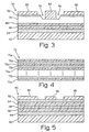
- FIG. 3 is similar to FIG. 2 but illustrates a second embodiment of the invention;
- FIG. 4 is an enlarged sectional view illustrating a superlattice layer structure of the embodiment of FIG. 3; and
- FIG. 5 is similar to FIG. 2, but illustrates a third embodiment of the present invention.
- Referring now to FIG. 2 of the drawing, a HEMT structure embodying the present invention is generally designated as 40, and includes a
substrate 42 formed of a suitable material such as GaAs, GaInAs, or InP, which may have a buffer layer (not shown) of, for example, AlInAs formed thereon. Achannel layer 44,spacer layer 46,donor layer 48, Schottkylayer 50, passivation orstop layer 52, Schottkylayer 54, andcap layer 56 are formed on thesubstrate 42 such that each successive layer overlies the previous layers. Arecess 58 is formed through thecap layer 56, and extends at least partially into the Schottkylayer 54. Asource 60 anddrain 62 are formed on thecap layer 56 on opposite sides of therecess 58. Agate 64 is formed on the bottom of therecess 58. - The HEMT 40 operates in a conventional manner, with electrons propagating through the
channel layer 44 between thesource 60 and drain 62 in response to a voltage applied thereacross. The magnitude of electron flow is determined by a voltage applied to thegate 64. Thedonor layer 48 andchannel layer 44 form a heterojunction structure, with mobile electrons from thedonor layer 48 being induced into thechannel layer 44 due to a space charge effect between thelayers 48 and 44 (which extends across the spacer layer 46). The absence of donor atoms in thechannel layer 44 greatly increases the mobility of electrons therein. The Schottkylayer 54 is provided to reduce the gate leakage current of the device. - The
spacer layer 46,donor layer 48, and Schottkylayers channel layer 44 andcap layer 56 are formed of a narrow bandgap material which does not include an oxidizable component, such as GaInAs or GaAs, and is lattice-matched to the wide bandgap material. In accordance with the present invention, the passivation orstop layer 52 is formed of a lattice-matched or pseudomorphic material, preferably the same narrow bandgap material which constitutes the channel andcap layers - As indicated at 66 in FIG. 2, portions of the Schottky
layer 54 on opposite sides of thegate 64 in therecess 58 are exposed to the atmosphere and may oxidize. However, the oxidation is prevented from spreading to thedonor layer 48 by theoverlying stop layer 52, which is formed of a non-oxidizable material. The addition of thestop layer 52 reduces the Schottky barrier height of the device to a small extent, but this is not a significant problem if thestop layer 52 is made sufficiently thin. - The Schottky
layer 50 is optional, and may be omitted in accordance with a particular application. The embodiment of FIG. 2 is particularly advantageous for forming discrete devices in GaInAs in which the spacing between thegate 64 andchannel layer 44 is the same for all devices on a wafer, and is determined by a common etching process step. - Typical values for the thicknesses of the component layers of the
structure 40 are as follows. However, these values are exemplary, and not to be construed as limiting the scope of the invention. - Channel layer 44 - 400 angstroms; spacer layer 46 -15 angstroms; donor layer 48 (doped with silicon) - 50 to 80 angstroms; Schottky layer 50 - 20 to 40 angstroms; stop layer 52 - as thin as possible, typically 5 to 15 angstroms; Schottky layer 54 - 150 to 200 angstroms; cap layer 56 - 50 to 75 angstroms. The thickness of the Schottky
layer 54 in therecess 58 under thegate 64 may be approximately 20 to 60 angstroms. - FIGs. 3 and 4 illustrate another embodiment of the present invention, in which like elements are designated by the same reference numerals used in FIG. 2. In a
transistor structure 70, thelayers superlattice 72 which is shown to an enlarged scale in FIG. 4. More specifically, thesuperlattice 72 is formed of alternating Schottky andstop sublayers superlattice 72 is equivalent to the Schottkylayers stop layer 52 of FIG. 2 taken in combination. Arecess 74 may be etched into thesuperlattice 72 to a depth which provides the desired gate to channel spacing and Schottky barrier height. Although edges of the Schottkysublayers 72a which are exposed by etching of therecess 74 are subject to oxidation, the etching is controlled to such an extent that at least onestop sublayer 72b is left unetched to sealingly overlie thedonor layer 48. - Typically, the thickness of the
superlattice 72 will be 200 to 250 angstroms. The Schottky sublayers 72a will be on the order of 30 angstroms thick, with thestop sublayers 72b will being 10 angstroms thick. The superlattice period (number of alternating sublayers) will be 5 to 6. - The embodiment of FIGs. 3 and 4 is advantageous in that it enables adjustment of the gate to channel spacing on an individual device basis. It also reduces the need for precise control over the gate region etch, in applications where such precision is a particularly undesirable requirement. In the embodiment of FIG. 2, the etching must be stopped before it reaches the
stop layer 52. If it did not, the oxidation could proceed through the underlying Schottky layer 50 (if provided) anddonor layer 48. The embodiment of FIGs. 3 and 4 allows greater latitude in etching, since a slight over or underetch will still provide at least onestop sublayer 72b under thegate 64. The embodiment of FIGs. 3 and 4 is particularly suitable for forming dissimilar devices, having different gate to channel spacings, in a material such as AlGaAs, which has a higher Schottky barrier height and lower gate leakage current than GaInAs. - FIG. 5 illustrates another embodiment of the present invention, with like elements again designated by the same reference numerals. A
transistor structure 80 includes aunitary cap layer 82 which further constitutes a stop layer. Thesource 84,drain 86, andgate 88 are formed on thecap layer 82. Thestructure 80 does not include a recess in which thegate 88 is formed, and is advantageous in that the etching steps required for forming a gate recess are eliminated. Thecap layer 82 sealingly overlies theSchottky layer 54 anddonor layer 48, preventing them from ever being exposed to an oxidizing atmosphere. The embodiment of FIG. 5 is suitable in applications where thecap layer 82 may be made thin enough to maintain an adequate Schottky barrier height for thegate 88, and where limited flexibility in selection of parameters such as the device pinch-off voltage is not a problem. - While several illustrative embodiments of the invention have been shown and described, numerous variations and alternate embodiments will occur to those skilled in the art, without departing from the spirit and scope of the invention. Accordingly, it is intended that the present invention not be limited solely to the specifically described illustrative embodiments. Various modifications are contemplated and can be made without departing from the spirit and scope of the invention as defined by the appended claims.
Claims (9)
- A field-effect transistor structure including a substrate; a channel layer formed of a narrow bandgap semiconductor material over said substrate; a donor layer formed of an oxidizable wide bandgap semiconductive material over said channel layer to form a heterojunction therewith; and a source, drain, and gate formed over said donor layer; and characterized by:
a single homogeneous oxidation-stop layer formed of a non-oxidizable narrow bandgap semiconductive material under said source, drain, and gate and sealingly extending over said donor layer. - A structure as in claim 1, further comprising a Schottky layer formed of said wide bandgap semiconductive material between said source, drain, and gate and said stop layer.
- A structure as in claim 2, in which said Schottky layer is formed with a recess extending partially therethrough;
said gate being formed on a bottom of said recess. - A structure as in claim 3, further comprising a cap layer formed of said narrow bandgap semiconductive material between said source and drain and said Schottky layer laterally external of said recess.
- A structure as in claim 2, further comprising a second Schottky layer formed of said wide bandgap semiconductive material between said stop layer and said donor layer.
- A structure as in claim 1, further comprising a Schottky layer formed of said wide bandgap semiconductive material between said source, drain, and gate and said donor layer.
- A structure as in claim 6, further comprising a cap layer formed of said narrow bandgap semiconductive material between said source, drain, and gate and said Schottky layer.
- A structure as in claim 6, in which said wide bandgap semiconductive material as AlInAs, and said narrow bandgap semiconductive material is GaInAs.
- A structure as in claim 6, in which said wide bandgap semiconductive material is AlGaAs, and said narrow bandgap semiconductive material is GaInAs.
Applications Claiming Priority (2)
| Application Number | Priority Date | Filing Date | Title |
|---|---|---|---|
| US50794590A | 1990-04-11 | 1990-04-11 | |
| US507945 | 1990-04-11 |
Publications (2)
| Publication Number | Publication Date |
|---|---|
| EP0452054A1 true EP0452054A1 (en) | 1991-10-16 |
| EP0452054B1 EP0452054B1 (en) | 1995-07-12 |
Family
ID=24020751
Family Applications (1)
| Application Number | Title | Priority Date | Filing Date |
|---|---|---|---|
| EP91303050A Expired - Lifetime EP0452054B1 (en) | 1990-04-11 | 1991-04-08 | HEMT structure with passivated structure |
Country Status (3)
| Country | Link |
|---|---|
| EP (1) | EP0452054B1 (en) |
| JP (1) | JP2609004B2 (en) |
| DE (1) | DE69111120T2 (en) |
Cited By (3)
| Publication number | Priority date | Publication date | Assignee | Title |
|---|---|---|---|---|
| EP0627768A2 (en) * | 1993-06-01 | 1994-12-07 | Nec Corporation | Field effect transistor with a Schottky gate |
| US5796127A (en) * | 1995-11-16 | 1998-08-18 | Mitsubishi Denki Kabushiki Kaisha | High electron mobility transistor |
| CN113889529A (en) * | 2019-03-28 | 2022-01-04 | 英诺赛科(珠海)科技有限公司 | Semiconductor device with a plurality of semiconductor chips |
Citations (1)
| Publication number | Priority date | Publication date | Assignee | Title |
|---|---|---|---|---|
| US4914488A (en) * | 1987-06-11 | 1990-04-03 | Hitachi, Ltd. | Compound semiconductor structure and process for making same |
Family Cites Families (7)
| Publication number | Priority date | Publication date | Assignee | Title |
|---|---|---|---|---|
| JPH0789584B2 (en) * | 1984-12-19 | 1995-09-27 | 日本電気株式会社 | Semiconductor device |
| JPS63228763A (en) * | 1987-03-18 | 1988-09-22 | Fujitsu Ltd | Semiconductor device |
| JPH088352B2 (en) * | 1987-09-17 | 1996-01-29 | 富士通株式会社 | Heterojunction FET |
| JPH01265573A (en) * | 1988-04-15 | 1989-10-23 | Mitsubishi Electric Corp | Manufacture of semiconductor device |
| JP2764942B2 (en) * | 1988-09-22 | 1998-06-11 | ソニー株式会社 | Solid-state imaging device |
| JP2617120B2 (en) * | 1988-09-26 | 1997-06-04 | 日本電信電話株式会社 | Field effect transistor and method of manufacturing the same |
| JP2630446B2 (en) * | 1988-10-12 | 1997-07-16 | 富士通株式会社 | Semiconductor device and manufacturing method thereof |
-
1991
- 1991-04-08 EP EP91303050A patent/EP0452054B1/en not_active Expired - Lifetime
- 1991-04-08 DE DE1991611120 patent/DE69111120T2/en not_active Expired - Fee Related
- 1991-04-09 JP JP3103866A patent/JP2609004B2/en not_active Expired - Lifetime
Patent Citations (1)
| Publication number | Priority date | Publication date | Assignee | Title |
|---|---|---|---|---|
| US4914488A (en) * | 1987-06-11 | 1990-04-03 | Hitachi, Ltd. | Compound semiconductor structure and process for making same |
Non-Patent Citations (2)
| Title |
|---|
| I.E.E.E. ELECTRON DEVICE LETTERS, vol. 9, no. 9, September 1988, pages 482-484; U.K. MISHRA et al.: "Ultra-high-speed digital circuit performance in 0.2-mum gate-length AlInAs/GaInAs HEMT technology" * |
| IEEE TRANSACTIONS ON ELECTRON DEVICES, vol. ED-33, no. 5, May 1986, pages 601-607; H. HIDA et al.: "A new low-noise AlGaAs/GaAs 2DEG FET with a surface undoped layer" * |
Cited By (6)
| Publication number | Priority date | Publication date | Assignee | Title |
|---|---|---|---|---|
| EP0627768A2 (en) * | 1993-06-01 | 1994-12-07 | Nec Corporation | Field effect transistor with a Schottky gate |
| EP0627768A3 (en) * | 1993-06-01 | 1995-06-07 | Nippon Electric Co | Field effect transistor with a Schottky gate. |
| US5635735A (en) * | 1993-06-01 | 1997-06-03 | Nec Corporation | Field effect transistor with an improved Schottky gate structure |
| US5796127A (en) * | 1995-11-16 | 1998-08-18 | Mitsubishi Denki Kabushiki Kaisha | High electron mobility transistor |
| CN113889529A (en) * | 2019-03-28 | 2022-01-04 | 英诺赛科(珠海)科技有限公司 | Semiconductor device with a plurality of semiconductor chips |
| CN113889529B (en) * | 2019-03-28 | 2024-01-23 | 英诺赛科(珠海)科技有限公司 | Semiconductor device with a semiconductor device having a plurality of semiconductor chips |
Also Published As
| Publication number | Publication date |
|---|---|
| DE69111120D1 (en) | 1995-08-17 |
| DE69111120T2 (en) | 1996-04-04 |
| JP2609004B2 (en) | 1997-05-14 |
| JPH04226041A (en) | 1992-08-14 |
| EP0452054B1 (en) | 1995-07-12 |
Similar Documents
| Publication | Publication Date | Title |
|---|---|---|
| US5172197A (en) | Hemt structure with passivated donor layer | |
| US5124762A (en) | Gaas heterostructure metal-insulator-semiconductor integrated circuit technology | |
| US20060197129A1 (en) | Buried and bulk channel finFET and method of making the same | |
| KR102630424B1 (en) | Enhancement-mode GaN transistor with selective and non-selective etch layers for improved uniformity of GaN spacer thickness | |
| US5405797A (en) | Method of producing a monolithically integrated millimeter wave circuit | |
| US5043777A (en) | Power FETS with improved high voltage performance | |
| US6248666B1 (en) | Process of manufacturing a semiconductor device including a buried channel field effect transistor | |
| US5334865A (en) | MODFET structure for threshold control | |
| US4652896A (en) | Modulation doped GaAs/AlGaAs field effect transistor | |
| JP3348673B2 (en) | Field effect transistor | |
| US5552330A (en) | Resonant tunneling fet and methods of fabrication | |
| EP0452054A1 (en) | HEMT structure with passivated structure | |
| US20080064155A1 (en) | Method for Producing a Multi-Stage Recess in a Layer Structure and a Field Effect Transistor with a Multi-Recessed Gate | |
| US5837570A (en) | Heterostructure semiconductor device and method of fabricating same | |
| US5389807A (en) | Field effect transistor | |
| US4774555A (en) | Power hemt structure | |
| JPH0271563A (en) | Semiconductor device, insulated gate type field effect transistor and schottky gate type field effect transistor | |
| KR940010557B1 (en) | Semiconductor device | |
| EP0271080B1 (en) | Indium-phosphide hetero-mis-gate field effect transistor | |
| US5994725A (en) | MOSFET having Schottky gate and bipolar device | |
| JPH0815205B2 (en) | Semiconductor device | |
| JPH01122173A (en) | Field-effect transistor | |
| WO1999027586A2 (en) | INxGa1-xP STOP-ETCH LAYER FOR SELECTIVE RECESS OF GALLIUM ARSENIDE-BASED EPTITAXIAL FIELD EFFECT TRANSISTORS AND PROCESS THEREFOR | |
| Bert et al. | Implications of the interface effects in the normally-off type GaAs MESFETs | |
| EP0308969A2 (en) | High electron mobility transistor structure |
Legal Events
| Date | Code | Title | Description |
|---|---|---|---|
| PUAI | Public reference made under article 153(3) epc to a published international application that has entered the european phase |
Free format text: ORIGINAL CODE: 0009012 |
|
| AK | Designated contracting states |
Kind code of ref document: A1 Designated state(s): DE FR |
|
| 17P | Request for examination filed |
Effective date: 19920323 |
|
| 17Q | First examination report despatched |
Effective date: 19940224 |
|
| GRAA | (expected) grant |
Free format text: ORIGINAL CODE: 0009210 |
|
| AK | Designated contracting states |
Kind code of ref document: B1 Designated state(s): DE FR |
|
| REF | Corresponds to: |
Ref document number: 69111120 Country of ref document: DE Date of ref document: 19950817 |
|
| ET | Fr: translation filed | ||
| PLBE | No opposition filed within time limit |
Free format text: ORIGINAL CODE: 0009261 |
|
| STAA | Information on the status of an ep patent application or granted ep patent |
Free format text: STATUS: NO OPPOSITION FILED WITHIN TIME LIMIT |
|
| 26N | No opposition filed | ||
| REG | Reference to a national code |
Ref country code: FR Ref legal event code: TP Ref country code: FR Ref legal event code: CD Ref country code: FR Ref legal event code: CA |
|
| PGFP | Annual fee paid to national office [announced via postgrant information from national office to epo] |
Ref country code: FR Payment date: 20020311 Year of fee payment: 12 |
|
| PGFP | Annual fee paid to national office [announced via postgrant information from national office to epo] |
Ref country code: DE Payment date: 20020314 Year of fee payment: 12 |
|
| PG25 | Lapsed in a contracting state [announced via postgrant information from national office to epo] |
Ref country code: DE Free format text: LAPSE BECAUSE OF NON-PAYMENT OF DUE FEES Effective date: 20031101 |
|
| PG25 | Lapsed in a contracting state [announced via postgrant information from national office to epo] |
Ref country code: FR Free format text: LAPSE BECAUSE OF NON-PAYMENT OF DUE FEES Effective date: 20031231 |
|
| REG | Reference to a national code |
Ref country code: FR Ref legal event code: ST |