EP0455966A2 - Compounding preprocessor for cache - Google Patents
Compounding preprocessor for cache Download PDFInfo
- Publication number
- EP0455966A2 EP0455966A2 EP91104318A EP91104318A EP0455966A2 EP 0455966 A2 EP0455966 A2 EP 0455966A2 EP 91104318 A EP91104318 A EP 91104318A EP 91104318 A EP91104318 A EP 91104318A EP 0455966 A2 EP0455966 A2 EP 0455966A2
- Authority
- EP
- European Patent Office
- Prior art keywords
- instruction
- instructions
- parallel
- tag
- storage mechanism
- Prior art date
- Legal status (The legal status is an assumption and is not a legal conclusion. Google has not performed a legal analysis and makes no representation as to the accuracy of the status listed.)
- Granted
Links
- 238000013329 compounding Methods 0.000 title claims abstract description 38
- 230000007246 mechanism Effects 0.000 claims description 49
- 238000000034 method Methods 0.000 abstract description 5
- 230000008569 process Effects 0.000 abstract description 4
- 150000001875 compounds Chemical class 0.000 description 42
- 238000010276 construction Methods 0.000 description 7
- 238000006073 displacement reaction Methods 0.000 description 6
- 238000004458 analytical method Methods 0.000 description 3
- 230000006872 improvement Effects 0.000 description 3
- 230000009471 action Effects 0.000 description 2
- 239000000872 buffer Substances 0.000 description 2
- 230000000694 effects Effects 0.000 description 2
- 238000005516 engineering process Methods 0.000 description 2
- 238000012986 modification Methods 0.000 description 2
- 230000004048 modification Effects 0.000 description 2
- 230000000063 preceeding effect Effects 0.000 description 2
- 238000004364 calculation method Methods 0.000 description 1
- 230000001419 dependent effect Effects 0.000 description 1
- 230000008520 organization Effects 0.000 description 1
- 238000012913 prioritisation Methods 0.000 description 1
- 230000004044 response Effects 0.000 description 1
Images


Classifications
-
- G—PHYSICS
- G06—COMPUTING; CALCULATING OR COUNTING
- G06F—ELECTRIC DIGITAL DATA PROCESSING
- G06F9/00—Arrangements for program control, e.g. control units
- G06F9/06—Arrangements for program control, e.g. control units using stored programs, i.e. using an internal store of processing equipment to receive or retain programs
- G06F9/30—Arrangements for executing machine instructions, e.g. instruction decode
- G06F9/38—Concurrent instruction execution, e.g. pipeline, look ahead
- G06F9/3818—Decoding for concurrent execution
- G06F9/382—Pipelined decoding, e.g. using predecoding
-
- G—PHYSICS
- G06—COMPUTING; CALCULATING OR COUNTING
- G06F—ELECTRIC DIGITAL DATA PROCESSING
- G06F9/00—Arrangements for program control, e.g. control units
- G06F9/06—Arrangements for program control, e.g. control units using stored programs, i.e. using an internal store of processing equipment to receive or retain programs
- G06F9/30—Arrangements for executing machine instructions, e.g. instruction decode
- G06F9/38—Concurrent instruction execution, e.g. pipeline, look ahead
- G06F9/3802—Instruction prefetching
-
- G—PHYSICS
- G06—COMPUTING; CALCULATING OR COUNTING
- G06F—ELECTRIC DIGITAL DATA PROCESSING
- G06F9/00—Arrangements for program control, e.g. control units
- G06F9/06—Arrangements for program control, e.g. control units using stored programs, i.e. using an internal store of processing equipment to receive or retain programs
- G06F9/30—Arrangements for executing machine instructions, e.g. instruction decode
- G06F9/38—Concurrent instruction execution, e.g. pipeline, look ahead
- G06F9/3836—Instruction issuing, e.g. dynamic instruction scheduling or out of order instruction execution
- G06F9/3853—Instruction issuing, e.g. dynamic instruction scheduling or out of order instruction execution of compound instructions
Definitions
- the computer system of Fig. 1 also includes an instruction fetch and issue mechanism coupled to the compound instruction cache 12 for supplying adjacent instructions stored therein to different ones of the functional instruction processing units 13-15 when the instruction tag fields indicate that they may be processed in parallel.
- This mechanism is represented by instruction fetch and issue unit 16.
- Fetch and issue unit 16 fetches instructions from cache 12, examines their tag fields and operation code (op code) fields and, based upon such examinations, sends the instructions to the appropriate ones of the functional units 13-15.
- the compound analyzer 22 includes instruction compatibility logic 30 for examining the op code of Instruction 0 and the op code of Instruction 1 and determining whether these two op codes are compatible for purposes of execution in parallel.
- Logic 30 is constructed in accordance with predetermined rules to select which pairs of op codes are compatible for execution in parallel. More particularly, logic 30 includes logic circuitry for implementing rules which define which types of instructions are compatible for parallel execution in the particular hardware configuration used for the computer system being considered. If the op codes for Instructions 0 and 1 are compatible, then logic 30 produces at its output a binary one level signal. If they are not compatible, logic 30 produces a binary zero value on its output line.
- Compound analyzer 22 further includes first register dependency logic 32 for detecting conflicts in the usage of the general purpose registers designated by the R1 and R2 fields of Instructions 0 and 1. These general purpose registers will be discussed in greater detail hereinafter.
- dependency logic 32 may be constructed to detect the occurrence of a data dependency condition wherein a second instruction (Instruction 1) needs to use the results obtained by the performance of the proceeding instruction (Instruction 0). In this case, either the second instruction can be executed by the dependency collapsing hardware, thus executing in parallel with the first instruction, or the execution of the second instruction must await completion of the execution of the preceeding instruction and, hence, cannot be executed in parallel with the preceeding instruction.
- Tag 2 has a binary value of one
- the status of its associated Instruction 2 is dependent on the binary value for Tag 3. If Tag 3 has a binary value of zero, then Instructions 2 and 3 can be executed in parallel. If, on the other hand, Tag 3 has a binary value of one, then Instruction 2 will be executed in a singular, nonparallel manner. It is noted that the logic implemented for the tag generator 26 does not permit the occurrence of two successive tag bits having binary values of zero.
- FIG. 7 there is shown a detailed example of how a computer system can be constructed for using the compounding tags of the present invention to provide parallel processing of machine-level computer instructions.
- the instruction compounding unit 20 used in Fig. 7 is assumed to be of the type described in Fig. 3 and, as such, it adds to each instruction a one-bit tag field. These tag fields are used to identify which pairs of instructions may be processed in the parallel. These tagged instructions are supplied to and stored into the compound instruction cache 12.
- Fetch/Issue control unit 60 fetches the tagged instructions from cache 12, as needed, and arranges for their processing by the appropriate one or ones of a plurality of functional instruction processing units 61, 62, 63 and 64.
- Fetch/Issue unit 60 examines the tag fields and op code fields of the fetched instructions. If the tag fields indicate that two successive instructions may be processed in parallel, then fetch/issue unit 60 assigns them to the appropriate ones of the functional units 61-64 as determined by their op codes and they are processed in parallel by the selected functional units. If the tag fields indicate that a particular instruction is to be processed in a singular, nonparallel manner, then fetch/issue unit 60 assigns it to a particular functional unit as determined by its op code and it is processed or executed by itself.
- the computer system embodiment of Fig. 7 also includes a set of general purpose registers 65 for use in executing some of the machine-level instructions.
- these general purpose registers 65 are used for temporarily storing data operands and address operands or are used as counters or for other data processing purposes.
- sixteen (16) such general purpose registers are provided.
- general purpose registers 65 are assumed to be of the multiport type wherein two or more registers may be accessed at the same time.
- the computer system of Fig. 7 further includes a high-speed data cache storage mechanism 66 for storing data operands obtained from the higher-level storage unit 10. Data in the cache 66 may also be transferred back to the higher-level storage unit 10. Data cache 66 may be of a known type and its operation relative to the higher-level storage 10 may be conducted in a known manner.
- the table of Fig. 9 gives further information on each of these Fig. 8 instructions.
- the R/M column in Fig. 9 indicates the content of a first field in each instruction which is typically used to identify the particular one of general purpose registers 65 which contains the first operand. An exception is the case of the Branch on Condition instruction, wherein the R/M field contains a condition code mask.
- the R/X column in Fig. 9 indicates the content of a second field in each instruction, which field is typically used to identify a second one of the general purpose registers 65. Such register may contain the second operand or may contain an address index value (X).
- the B column in Fig. 9 indicates the content of a third possible field in each instruction, which field may identify a particular one of the general purpose registers 65 which contains a base address value.
- the branch unit 61 commences to calculate the potential branch address (0 + R7 + 20) and at the same time compares the condition code obtained from the previous Compare instruction with the condition code mask M. If the condition code value is the same as the mask code value, the necessary branch condition is met and the branch address calculated by the branch unit 61 is thereupon loaded into an instruction counter in control unit 60. This instruction counter controls the fetching of the instructions from the compound instruction cache 12. If, on the other hand, the condition is not met (that is, the condition code set by the previous instruction does not have a value of eight), then no branch is taken and no branch address is supplied to the instruction counter in control unit 60.
- Fig. 8 The foregoing instruction sequence of Fig. 8 is intended as an example only.
- the computer system embodiment of Fig. 7 is equally capable of processing various and sundry other instruction sequences.
Abstract
Description
- The present United States patent application is related to the following copending United States patent applications:
- (1) Application Serial No: 07/519,384 (IBM Docket EN9-90-020), filed May 4, 1990, entitled "Scalable Compound Instruction Set Machine Architecture", the inventors being Stamatis Vassiliadis et al;
- (2) Application Serial No: 07/519,382 (IBM Docket EN9-90-019), filed May 4, 1990, entitled "General Purpose Compound Apparatus For Instruction-Level Parallel Processors", the inventors being Richard J. Eickemeyer et al;
- (3) Application Serial No: 07/504,910 (IBM Docket EN9-90-014), filed April 4, 1990, entitled "Data Dependency Collapsing Hardware Apparatus", the inventors being Stamatis Vassiliadis et al.
- These copending applications and the present application are owned by one and the same assignee, namely, International Business Machines Corporation of Armonk, New York.
- The descriptions set forth in these copending applications are hereby incorporated into the present application by this reference thereto.
- This invention relates to digital computers and digital data processors and particularly to digital computers and data processors capable of processing two or more instructions in parallel.
- The performance of traditional computers which execute instructions one at a time in a sequential manner has improved significantly in the past largely due to improvements in circuit technology. Such one-at-a-time instruction execution computers are sometimes referred to as "scalar" computers or processors. As the circuit technology is pushed to its limits, computer designers have had to investigate other means to obtain significant performance improvements.
- Recently, so called "super scalar" computers have been proposed which attempt to increase performance by executing more than one instruction at a time from a single instruction stream. Such proposed super scalar machines typically decide at instruction execution time if a given number of instructions may be executed in parallel. Such decision is based on the operation codes (op codes) of the instructions and on data dependencies which may exist between adjacent instructions. The op codes determine the particular hardware components each of the instructions will utilize and, in general, it is not possible for two or more instructions to utilize the same hardware component at the same time nor to execute an instruction that depends on the results of a previous instruction (data dependency). These hardware and data dependencies prevent the execution of some instruction combinations in parallel. In this case, the affected instructions are instead executed by themselves in a non-parallel manner. This, of course, reduces the performance of a super scalar machine.
- Proposed super scalar computers provide some improvement in performance but also have disadvantages which it would be desirable to minimize. For one thing, deciding at instruction execution time which instructions can be executed in parallel takes a small, but noticeable, amount of time which cannot be very readily masked by overlapping it with other normal machine operations. This disadvantage becomes more pronounced as the complexity of the instruction set architecture increases. Another disadvantage is that the decision making must be repeated all over again each time the same instructions are to be executed a second or further time.
- As discussed in copending application Serial No. 08/519,384 (IBM Docket EN9-90-020), one of the attributes of a Scalable Compound Instruction Set Machine (SCISM) is: Don't do the parallel execution decision making at execution time. Do it at an earlier point in the overall instruction handling process. For example, do it ahead of the instruction buffer in those machines which have instruction buffers or instruction stacks. For another example, do it ahead of the instruction cache in those machines which flow the instructions through a cache unit.
- Another attribute of a SCISM machine is to record the results of the parallel execution decision making so that such results are available in the event that those same instructions are used a second or further time.
- In one embodiment of the present invention, the recording of the parallel execution decision making is accomplished by generating tags which are added to or inserted into the individual instructions in an instruction stream. These tags tell whether the instructions can be executed in parallel or whether they need to be executed one at a time. This instruction tagging process is sometimes referred to herein as "compounding". It serves, in effect, to combine two or more individual instructions into a single compound instruction for parallel processing purposes.
- In a particularly advantageous embodiment of the present invention, the computer is one which includes a cache storage mechanism for temporarily storing machine instructions in their journey from a higher-level storage unit of the computer to the instruction execution units of the computer and the compounding or instructing tagging process is performed intermediate to the higher-level storage unit and the cache storage mechanism so that there is stored in the cache storage mechanism both instructions and compounding tags. As is known, the use of a well-designed cache storage mechanism, in and of itself, serves to improve the overall performance of a computer. And the storing of the compounding tags into the cache storage mechanism enables the tags to be used over and over again so long as the instructions in question remain in the cache storage mechanism. As is known, instructions frequently remain in a cache long enough to be used more than once.
- For a better understanding of the present invention, together with other and further advantages and features thereof, reference is made to the following description taken in connection with the accompanying drawings, the scope of the invention being pointed out in the appended claims.
- Referring to the drawings:
- Fig. 1
- shows a representative embodiment of a portion of a digital computer system constructed in accordance with the present invention;
- Fig. 2
- shows a length of an instruction stream having compounding tags or tag fields associated with the instructions;
- Fig. 3
- shows in greater detail the internal construction of a representative embodiment of an instruction compounding unit which can be used in the computer system of Fig. 1;
- Fig. 4
- shows in greater detail a representative internal construction for each of the compound analyzer units of Fig. 3;
- Fig. 5
- shows an example of logic circuitry that may be used to implement the compound analyzer and tag generator portions of Fig. 3 which produce the compounding tags for the first three instructions in the instruction stream;
- Fig. 6
- is a table used in explaining the operation of the Fig. 5 example;
- Fig. 7
- shows a representative embodiment of a portion of a digital computer system and is used to explain how the compounded instructions may be processed in parallel by multiple functional instructions processing units;
- Fig. 8
- shows an example of a particular sequence of instructions which may be processed by the computer system of Fig. 7; and
- Fig. 9
- is a table used in explaining the processing of the Fig. 8 instruction sequence by the computer system of Fig. 7.
- Referring to Fig. 1 of the drawings, there is shown a representative embodiment of a portion of a digital computer system or digital data processing system constructed in accordance with the present invention. This computer system is capable of processing two or more instructions in parallel. It includes a first storage mechanism for storing instructions and data to be processed. This storage mechanism is identified as higher-
level storage 10. Thisstorage 10 is a larger-capacity, lower-speed storage mechanism and may be, for example, a large- capacity system storage unit or the lower portion of a comprehensive hierarchical storage system or the like. - The computer system of Fig. 1 also includes an instruction compounding mechanism for receiving instructions from the higher-
level storage 10 and associating with these instructions tag fields which indicate which of these instructions may be processed in parallel with one another. This instruction compounding mechanism is represented byinstruction compounding unit 11. Thisinstruction compounding unit 11 analyzes the incoming instructions for determining which ones may be processed in parallel. Furthermore,instruction compounding unit 11 produces for these analyzed instructions tag information or tag fields which indicate which instructions may be processed in parallel with one another and which ones may not be processed in parallel with one another. - The Fig. 1 system further includes a second storage mechanism coupled to the
instruction compounding mechanism 11 for receiving and storing the analyzed instructions and their associated tag fields. This second or further storage mechanism is represented bycompound instruction cache 12.Cache 12 is a smaller-capacity, higher-speed storage mechanism of the kind commonly used for improving the performance rate of a computer system by reducing the frequency of having to access the lower-speed storage mechanism 10. - The Fig. 1 system further includes a plurality of functional instruction processing units which operate in parallel with one another. These functional instruction processing units are represented by
functional units - The computer system of Fig. 1 also includes an instruction fetch and issue mechanism coupled to the
compound instruction cache 12 for supplying adjacent instructions stored therein to different ones of the functional instruction processing units 13-15 when the instruction tag fields indicate that they may be processed in parallel. This mechanism is represented by instruction fetch andissue unit 16. Fetch andissue unit 16 fetches instructions fromcache 12, examines their tag fields and operation code (op code) fields and, based upon such examinations, sends the instructions to the appropriate ones of the functional units 13-15. - If a desired instruction is resident in the
compound instruction cache 12, the appropriate address is sent to thecache 12 to fetch therefrom the desired instruction. This is sometimes referred to as a "cache hit". If the requested instruction does not reside incache 12, then it must be fetched from the higher-level storage 10 and brought intocache 12. This is sometimes referred to as a "cache miss". When a miss occurs, the address of the requested instruction is sent to thehigher level storage 10. In response thereto,storage 10 commences the transfer out or read out of a line of instructions which includes the requested instruction. These instructions are transferred to the input of theinstruction compounding unit 11, which unit proceeds to analyze these incoming instructions and generate the appropriate tag field for each instruction. The tagged instructions are thereafter supplied to thecompound instruction cache 12 and stored therein for subsequent use, if needed, by thefunctional units - The instruction analysis performed in the
instruction compounding unit 11 does require a certain relatively small amount of time. - However, the instruction compounding analysis is performed only when an instruction cache miss occurs and is thus relatively infrequent.
- Fig. 2 shows a portion of a stream of compounded or tagged instructions as they might appear at the output of the
instruction compounding unit 11 of Fig. 1. As is seen, each instruction (Instr.) has a tag field added to it by theinstruction compounding unit 11. The tagged instructions, like those shown in Fig. 2, are stored into thecompound instruction cache 12. As needed, the tagged instructions incache 12 are fetched by the instruction fetch andissue unit 16. As the tagged instructions are received by fetch andissue unit 16, their tag fields are examined to determine if they may be processed in parallel and their operation code (op code) fields are examined to determine which of the available functional units is most appropriate for their processing. If the tag fields indicate that two or more of the instructions are suitable for processing in parallel, then they are sent to the appropriate ones of the functional units in accordance with the codings of their op code fields. Such instructions are then processed concurrently with one another by their respective functional units. - When an instruction is encountered that is not suitable for parallel processing, then it is sent to the appropriate functional unit as determined by its op code and it is thereupon processed alone and by itself by the selected functional unit.
- In the most perfect case, where plural instructions are always being processed in parallel, the instruction execution rate of the computer system would be N times as great as for the case where instructions are executed one at a time, with N being the number of instructions in the groups which are being processed in parallel.
- Fig. 3 shows in greater detail the internal construction of a representative embodiment of an instruction compounding unit constructed in accordance with the present invention. This
instruction compounding unit 20 is suitable for use as theinstruction compounding unit 11 of Fig. 1. Theinstruction compounding unit 20 of Fig. 3 is designed for the case where a maximum of two instructions at a time may be processed in parallel. In this case, a one-bit tag field is used. A tag bit value of "one" means that the instruction is a "first" instruction. A tag bit value of "zero" means that the instruction is "second" instruction and may be executed in parallel with the proceeding first instruction. An instruction having a tag bit value of one may be executed either by itself or at the same time and in parallel with the next instruction, depending on the tag bit value for such next instruction. - Each pairing of an instruction having a tag bit value of one with a succeeding instruction having a tag bit value of zero forms a compound instruction for parallel execution purposes, that is, the instructions in such a pair may be processed in parallel with one another. When the tag bits for two succeeding instructions each have a value of one, the first of these instructions is executed by itself in a nonparallel manner. In the worst possible case, all of the instructions in the sequence would have a tag bit value of one. In this worst case, all of the instructions would be executed one at a time in a nonparallel manner.
- The
instruction compounding unit 20 of Fig. 3 includes a plural-instruction instruction register 21 for receiving a plurality of successive instructions from the higher-level storage unit 10.Instruction compounding unit 20 also includes a plurality of rule-based instruction analyzer mechanisms. Each such instruction analyzer mechanism analyzes a different pair of side-by-side instructions in theinstruction register 21 and produces a compoundability signal which indicates whether or not the two instructions in its pair may be processed in parallel. In Fig. 3, there are shown a plurality of compound analyzer units 22-25. Each of these compound analyzer units 22-25 includes two of the instruction analyzer mechanisms just mentioned. Thus, each of these analyzers units 22-25 produces two of the compoundability signals. For example, the firstcompound analyzer unit 22 produces a first compoundability signal M01 which indicates whether or notInstructions Compound analyzer unit 22 also produces a second compoundability signal M12 which indicates whether or notInstructions - In a similar manner, the second
compound analyzer unit 23 produces a first compoundability signal M23 which indicates whether or notInstructions Instructions third compound analyzer 24 produces a first compoundability signal M45 which indicates whether or notInstructions Instructions fourth compound analyzer 25 produces a first compoundability signal M67 which indicates whether or notInstructions Instructions - The
instruction compounding unit 20 further includes atag generating mechanism 26 responsive to the compoundability signals appearing at the outputs of the analyzer units 22-23 for generating the individual tag fields for the different instructions in theinstruction register 21. These tag fields T0, T1, T2, etc. are supplied to a taggedinstruction register 27, as are the instructions themselves, the latter being obtained from theinput instruction register 21. In this manner, there is provided in the compounding unit output register 27 a tag field T0 forInstruction 0, a tag field T1 forInstruction 1, etc. - In the present embodiment, each tag field T0, T1, T2, etc. is comprised of a single binary bit. A tag bit value of "one" indicates that the immediately following instruction to which it is attached is a "first" instruction. A tag bit value of "zero" indicates that the immediately following instruction is a "second" instruction. An instruction having a tag bit value of one followed by an instruction having a tag bit value of zero indicates that those two instructions may be executed in parallel with one another. The tagged instructions in the compounding unit output register 27 are supplied to the input of the
compound instruction cache 12 of Fig. 1 and are stored into suchcompound instruction cache 12. - It should be noted that the amount of register hardware shown in Fig. 3 can be reduced by storing the compound instructions directly to the compound instruction cache.
- Referring now to Fig. 4, there is shown in greater detail the internal construction used for the
compound analyzer unit 22 of Fig. 3. The other compound analyzer units 23-25 are of a similar construction. As shown in Fig. 4, thecompound analyzer 22 includesinstruction compatibility logic 30 for examining the op code ofInstruction 0 and the op code ofInstruction 1 and determining whether these two op codes are compatible for purposes of execution in parallel.Logic 30 is constructed in accordance with predetermined rules to select which pairs of op codes are compatible for execution in parallel. More particularly,logic 30 includes logic circuitry for implementing rules which define which types of instructions are compatible for parallel execution in the particular hardware configuration used for the computer system being considered. If the op codes forInstructions logic 30 produces at its output a binary one level signal. If they are not compatible,logic 30 produces a binary zero value on its output line. -
Compound analyzer 22 further includes a secondinstruction compatibility logic 31 for examining the op codes ofInstructions Logic 31 is constructed in the same manner aslogic 30 in accordance with the same predetermined rules used forlogic 30 to select which pairs of op codes are compatible for execution in parallel for the case ofInstructions logic 31 includes logic circuitry for implementing rules which define which types of instructions are compatible for parallel execution, these rules being the same as those used inlogic 30. If the op codes forInstructions logic 31 produces a binary one level output. Otherwise, it produces a binary zero level output. -
Compound analyzer 22 further includes firstregister dependency logic 32 for detecting conflicts in the usage of the general purpose registers designated by the R1 and R2 fields ofInstructions dependency logic 32 may be constructed to detect the occurrence of a data dependency condition wherein a second instruction (Instruction 1) needs to use the results obtained by the performance of the proceeding instruction (Instruction 0). In this case, either the second instruction can be executed by the dependency collapsing hardware, thus executing in parallel with the first instruction, or the execution of the second instruction must await completion of the execution of the preceeding instruction and, hence, cannot be executed in parallel with the preceeding instruction. (It is noted that a technique for circumventing some data dependencies of this type will be discussed hereinafter.) If there are no register dependencies which prevent execution ofInstructions logic 32 is given a binary value of one. If there is a dependency, then it is given a binary value of zero. -
Compound analyzer 22 further includes secondregister dependency logic 33 for detecting conflicts in the usage of the general purpose registers designated by the R1 and R2 fields ofInstructions logic 33 is of the same construction as the previously discussedlogic 32 and produces a binary one level output if there are no register dependencies or the register dependencies can be executed by the data dependency collapsing hardware, and a binary zero level output otherwise. - The output lines from the
instruction compatibility logic 30 and theregister dependency logic 32 are connected to the two inputs of an ANDcircuit 34. The output line of AND 34 has a binary one value if the two op codes being considered are compatible and if there are no register dependencies. This binary one value on the AND 34 output line indicates that the two instructions being considered are compoundable, that is, are executable in parallel. If, on the other hand, the AND 34 output line has a binary value of zero, then the two instructions are not compoundable. Thus, there is produced on the AND 34 output line a first compoundability signal M01 which indicates whether or notInstructions tag generator 26. - The output lines from the
second compatibility logic 31 and thesecond dependency logic 33 are connected to the two inputs of ANDcircuit 35. AND 35 produces on its output line a second compoundability signal M12 which has a binary value of one if the two op codes being considered (op codes forInstructions 1 and 2) are compatible and if there are no register dependencies forInstructions tag generator 26. - The other compound analyzers 23-25 shown in Fig. 3 are of the same internal construction as shown in Fig. 4 for the
first compound analyzer 22. - Referring now to Fig. 5, there is shown an example of the logic circuitry that can be used to implement the
compound analyzer 22 and the portion of thetag generator 26 which is used to generate the first three tags,Tag 0,Tag 1 andTag 2. For the example of Fig. 5, it is assumed that there are two categories of instructions which are designated as category A and category B. The rules for compounding these categories of instructions are assumed to be as follows: - (1) A can always compound with A
- (2) A can never compound with B
- (3) B can never compound with B
- (4) B can always compound with A
- (5) Rule (4) has preference over Rule (1).
- Note that these rules are sensitive to the order of occurrence of the instructions.
- It is further assumed that these rules are such that when they are observed, there will be no problems with register dependencies because the rules implicitly indicate that in case there is any interlock, such an interlock is always executable by the data dependency collapsing hardware. In other words, it is assumed for the Fig. 5 example, that the
register dependency logics circuits logic 30 becomes the M01 signal and the output oflogic 31 becomes the M12 signal. - For these assumptions, Fig. 5 shows the internal logic circuitry that may be used for the
instruction compatibility logic 30 and theinstruction compatibility logic 31 of Fig. 4. With reference to Fig. 5, theinstruction compatibility logic 30 includesdecoders 40 and 41, ANDcircuits circuit 44. The secondinstruction compatibility logic 31 includesdecoders 41 and 45, ANDcircuits 46 and 47 and OR circuit 48. The middle decoder 41 is shared by bothlogics - The
first logic 30 examines the op codes OP0 and OP1 ofInstructions Decoder 40 looks at the op code of the first instruction and if it is a category A op code, the A output line ofdecoder 40 is set to the one level. If OP0 is a category B op code, then the B output line ofdecoder 40 is set to a one level. If OP0 belongs to neither category A nor category B, then both outputs ofdecoder 40 are at the binary zero level. The second decoder 41 does a similar kind of decoding for the second op code OP1. - AND
circuit 42 implements Rule (1) above. If OP0 is a category A op code and OP1 is also a category A op code, then AND 42 produces a one level output. Otherwise, the output of AND 42 is a binary zero level. AND 43 implements Rule (4) above. If the first op code is a category B op code and the second op code is a category A op code, then AND 43 produces a one level output. Otherwise, it produces a zero level output. If either AND 42 or AND 43 produces a one level output, this drives the output of ORcircuit 44 to the one level, in which case, the compoundability signal M01 has a value of one. This one value indicates that the first and second instructions (Instructions 0 and 1) are compatible for parallel execution purposes. - If any other combination of op code categories is detected by
decoders 40 and 41, then the outputs of AND 42 and AND 43 remain at the zero level and compoundability signal M01 has the noncompoundability-indicating value of zero. Thus, the occurrence of the combinations indicated by Rules (2) and (3) above do not satisfy AND's 42 and 43 and M01 remains at the zero level. If there are further catorgories of op codes in addition to catorgories A and B, their occurrences in the instruction stream do not activate the outputs ofdecoders 40 and 41. Hence, they likewise result in an M01 compoundability signal value of zero. - The second
instruction compatibility logic 31 performs a similar type of op code analysis for the second and third instructions (Instructions 1 and 2). If the second op code OP1 is a category A op code and the third op code OP2 is a category A opcode, then, per Rule (1), AND 46 produces a one level output and the second compoundability signal M12 is driven to the compoundability-indicating binary one level. If, on the other hand OP1 is a category B opcode and OP2 is a category A opcode, then, per Rule (4), AND 47 is activated to produce a binary one level for the second compoundability signal M12. For any op code combinations other than those set forth in Rules (1) and (4), the M12 signal has a value of zero. - The M01 and M12 compoundability signals are supplied to the
tag generator 26. Fig. 5 shows the logic circuitry that can be used intag generator 26 to respond to the M01 and M12 compoundability signals to produce the desired tag bit values forTags tag generator 26 forTags - For the case of the first row in Fig. 6, all three tag bits have a value of one. This means that each of
Instructions Instructions Tag 0 has the required one value andTag 1 has the required zero value. For the third row in Fig. 6,Instruction 0 will be executed in a singular manner, whileInstructions Instructions - For those cases where
Tag 2 has a binary value of one, the status of its associatedInstruction 2 is dependent on the binary value forTag 3. IfTag 3 has a binary value of zero, thenInstructions Tag 3 has a binary value of one, thenInstruction 2 will be executed in a singular, nonparallel manner. It is noted that the logic implemented for thetag generator 26 does not permit the occurrence of two successive tag bits having binary values of zero. - An examination of Fig. 6 reveals the logic needed to be implemented by the portion of
tag generator 26 shown in Fig. 5. As indicated in Fig. 6,Tag 0 will always have a binary value of one. This is accomplished by providing a constant binary value of one to taggenerator output line 50 which constitutes theTag 0 output line. An examination of Fig. 6 further reveals that the bit value forTag 1 is always the opposite of the bit value of the M01 compoundability signal. This result is accomplished by connectingoutput line 51 forTag 1 to the output ofNOT circuit 52, the input of which is connected to the M01 signal line. - The binary level on
Tag 2output line 53 is determined by anOR circuit 54 and aNOT circuit 55. One input of OR 54 is connected to the M01 line. If M01 has a value of one, thenTag 2 has a value of one. This takes care of theTag 2 values in the second and fourth rows of Fig. 6. The other input of OR 54 is connected by way of NOT 55 to the M12 signal line. If M12 has a binary value of zero, this value is inverted by NOT 55 to supply a binary one value to the second input of OR 54. This causes theTag 2output line 53 to have a binary one value. This takes care of theTag 2 value for row one of Fig. 6. Note that for therow 3 case,Tag 2 must have a value of zero. This will occur because, for this case, M01 will have a value of zero and M12 will have a value of one which is inverted by NOT 55 to produce a zero at the second input of OR 54. - Implicit in the logic of Fig. 6 is a prioritization rule for the row four case where each of M01 and M12 has a binary value of one. This row four case can be produced by an instruction category sequence of BAA. This could be implemented by a tag sequence of 101 as shown in Fig. 6 or, alternatively, by a tag sequence of 110. In the present embodiment, Rule (5) is followed and the 101 sequence shown in Fig. 6 is chosen. In other words, the BA pairing is given preference over the AA pairing.
- The 1,1 pattern for M01 and M12 can also be produced by an op code sequence of AAA. In this case, the 101 tag sequence of Fig. 6 is again selected. This is better because it provides a one value for
Tag 2 and, hence, potentially enablesInstruction 2 to be compounded withInstruction 3 ifInstruction 2 is compatible withInstruction 3. - Referring to Fig. 7, there is shown a detailed example of how a computer system can be constructed for using the compounding tags of the present invention to provide parallel processing of machine-level computer instructions. The
instruction compounding unit 20 used in Fig. 7 is assumed to be of the type described in Fig. 3 and, as such, it adds to each instruction a one-bit tag field. These tag fields are used to identify which pairs of instructions may be processed in the parallel. These tagged instructions are supplied to and stored into thecompound instruction cache 12. Fetch/Issue control unit 60 fetches the tagged instructions fromcache 12, as needed, and arranges for their processing by the appropriate one or ones of a plurality of functionalinstruction processing units Issue unit 60 examines the tag fields and op code fields of the fetched instructions. If the tag fields indicate that two successive instructions may be processed in parallel, then fetch/issue unit 60 assigns them to the appropriate ones of the functional units 61-64 as determined by their op codes and they are processed in parallel by the selected functional units. If the tag fields indicate that a particular instruction is to be processed in a singular, nonparallel manner, then fetch/issue unit 60 assigns it to a particular functional unit as determined by its op code and it is processed or executed by itself. - The first
functional unit 61 is a branch instruction processing unit for processing branch type instructions. The secondfunctional unit 62 is a three input address generation arithmetic and logic unit (ALU) which is used to calculate the storage address for instructions which transfer operands to or from storage. The thirdfunctional unit 63 is a general purpose arithmetic and logic unit (ALU) which is used for performing mathematical and logical type operations. The fourthfunctional unit 64 in the present example is a data dependency collapsing ALU of the kind described in the above-referenced copending application Serial No: 07/504,910 (IBM Docket EN9-90-014). Thisdependency collapsing ALU 64 is a three-input ALU capable of performing two arithmetical/logical operations in a single machine cycle. - The computer system embodiment of Fig. 7 also includes a set of general purpose registers 65 for use in executing some of the machine-level instructions. Typically, these general purpose registers 65 are used for temporarily storing data operands and address operands or are used as counters or for other data processing purposes. In a typical computer system, sixteen (16) such general purpose registers are provided. In the present embodiment, general purpose registers 65 are assumed to be of the multiport type wherein two or more registers may be accessed at the same time.
- The computer system of Fig. 7 further includes a high-speed data
cache storage mechanism 66 for storing data operands obtained from the higher-level storage unit 10. Data in thecache 66 may also be transferred back to the higher-level storage unit 10.Data cache 66 may be of a known type and its operation relative to the higher-level storage 10 may be conducted in a known manner. - Fig. 8 shows an example of a compounded or tagged instruction sequence which may be processed by the computer system of Fig. 7. The Fig. 8 example is composed of the following instructions in the following sequence: Load, Add, Compare, Branch on Condition and Store. These are identified as instructions I1-I5, respectively. The tag bits for these instructions are 1,1,0,1 and 0, respectively. Because of the organization of the machine shown in Fig. 7, the Load instruction is processed in a singular manner by itself. The Add and Compare instructions are treated as a compound instruction and are processed in parallel with one another. The Branch and Store instructions are also treated as a compound instruction and are also processed in parallel with one another.
- The table of Fig. 9 gives further information on each of these Fig. 8 instructions. The R/M column in Fig. 9 indicates the content of a first field in each instruction which is typically used to identify the particular one of general purpose registers 65 which contains the first operand. An exception is the case of the Branch on Condition instruction, wherein the R/M field contains a condition code mask. The R/X column in Fig. 9 indicates the content of a second field in each instruction, which field is typically used to identify a second one of the general purpose registers 65. Such register may contain the second operand or may contain an address index value (X). The B column in Fig. 9 indicates the content of a third possible field in each instruction, which field may identify a particular one of the general purpose registers 65 which contains a base address value. A zero in the B column indicates the absence of a B field or the absence of a corresponding address component in the B field. The D field of Fig. 9 indicates the content of a further field in each instruction which, when used for address generation purposes, includes an address displacement value. A zero in the D column may also indicate the absence of a corresponding field in the particular instruction being considered or, alternatively, an address displacement value of zero.
- Considering now the processing of the Load instruction of Fig. 8, the fetch/
issue control unit 60 determines from the tag bits for this Load instruction and the following Add instruction that the Load instruction is to be processed in a singular manner by itself. The action to be performed by this Load instruction is to fetch an operand from storage, in this case thedata cache 66, and to place such operand into the R2 general purpose register. The storage address from which this operand is to be fetched is determined by adding together the index value in register X, the base value in register B and the displacement value D. The fetch/issue control unit 60 assigns this address generation operation to theaddress generation ALU 62. In this case,ALU 62 adds together the address index value in register X (a value of zero in the present example), the base address value contained in general purpose register R7 and the displacement address value (a value of zero in the present example) contained in the instruction itself. The resulting calculated storage address appearing at the output ofALU 62 is supplied to the address input ofdata cache 66 to access the desired operand. This accessed operand is loaded into the R2 general purpose register in register set 65. - Considering now the processing of the Add and Compare instructions, these instructions are fetched by the fetch/
issue control unit 60. Thecontrol unit 60 examines the compounding tags for these two instructions and notes that they may be executed in parallel. As seen from Fig. 9, the Compare instruction has an apparent data dependency on the Add instruction since the Add must be completed before R3 can be compared. This dependency, however, can be handled by the datadependency collapsing ALU 64. Consequently, these two instructions can be processed in parallel in the Fig. 7 configuration. In particular, thecontrol unit 60 assigns the processing of the Add instruction toALU 63 and assigns the processing of the Compare instruction to thedependency collapsing ALU 64. -
ALU 63 adds the contents of the R2 general purpose register to the contents of the R3 general purpose register and places the result of the addition back into the R3 general purpose register. At the same time, thedependency collapsing ALU 64 performs the following mathematical operation:
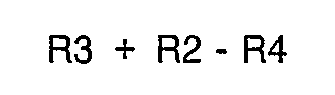
- The condition code for the result of this operation is sent to a condition code register located in
branch unit 61. The data dependency is collapsed becauseALU 64, in effect, calculates the sum of R3 + R2 and then compares this sum with R4 to determine the condition code. In this manner,ALU 64 does not have to wait on the results from theALU 63 which is performing the Add instruction. In this particular case, the numerical results calculated by the ALU 64 and appearing at the output ofALU 64 is not supplied back to the general purpose registers 65. In this case,ALU 64 merely sets the condition code. - Considering now the processing of the Branch instruction and the Store instruction shown in Fig. 8, these instructions are fetched from the
compound instruction cache 12 by the fetch/issue control unit 60.Control unit 60 determines from the tag bits for these instructions that they may be processed in parallel with one another. It further determines from the op codes of the two instructions that the Branch instruction should be processed by thebranch unit 61 and the Store instruction should be processed by theaddress generation ALU 62. In accordance with this determination, the mask field M and the displacement field D of the Branch instruction are supplied to thebranch unit 61. Likewise, the address index value in register X and the address base value in register B for this Branch instruction are obtained from the general purpose registers 65 and supplied to thebranch unit 61. In the present example, the X value is zero and the base value is obtained from the R7 general purpose register. The displacement value D has a hexadecimal value of twenty, while the mask field M has a mask position value of eight. - The
branch unit 61 commences to calculate the potential branch address (0 + R7 + 20) and at the same time compares the condition code obtained from the previous Compare instruction with the condition code mask M. If the condition code value is the same as the mask code value, the necessary branch condition is met and the branch address calculated by thebranch unit 61 is thereupon loaded into an instruction counter incontrol unit 60. This instruction counter controls the fetching of the instructions from thecompound instruction cache 12. If, on the other hand, the condition is not met (that is, the condition code set by the previous instruction does not have a value of eight), then no branch is taken and no branch address is supplied to the instruction counter incontrol unit 60. - At the same time that the
branch unit 61 is busy carrying out its processing actions for the Branch instruction, theaddress generation ALU 62 is busy doing the address calculation (0 + R7 + 0) for the Store instruction. The address calculated byALU 62 is supplied to thedata cache 66. If no branch is taken by thebranch unit 61, then the Store instruction operates to store the operand in the R3 general purpose register into thedata cache 66 at the address calculated byALU 62. If, on the other hand, the branch condition is met and the branch is taken, then the contents of the R3 general purpose register is not stored into thedata cache 66. - The foregoing instruction sequence of Fig. 8 is intended as an example only. The computer system embodiment of Fig. 7 is equally capable of processing various and sundry other instruction sequences. The example of Fig. 8, however, clearly shows the utility of the compound instruction tags in determining which pairs of instructions may be processed in parallel with one another.
- While there have been described what are at present considered to be preferred embodiments of this invention, it will be obvious to those skilled in the art that various changes and modifications may be made therein without departing from the invention, and it is, therefore, intended to cover all such changes and modifications as fall within the true spirit and scope of the invention.
Claims (8)
- In a digital computer system capable of processing two or more instructions in parallel, the combination comprising:
a larger-capacity, lower-speed storage mechanism for storing instructions to be processed;
a smaller-capacity, higher-speed storage mechanism for storing instructions with associated tag information;
and an instruction compounding mechanism coupled between the lower-speed storage mechanism and the higher-speed storage mechanism for receiving instructions from the lower-speed storage mechanism, for analyzing these instructions and producing tag information which indicates which instructions may be processed in parallel with one another and for supplying these instructions and associated tag information to the higher-speed storage mechanism for storage therein. - The combination of claim 1 wherein the higher-speed storage mechanism is a cache storage mechanism.
- The combination of claim 1 or 2 wherein the tag information is comprised of a plurality of tag fields, a different one of which is associated with each instruction analyzed by the instruction compounding mechanism.
- The combination of one of claims 1 to 3 wherein the computer system includes a plurality of functional instruction processing units which operate in parallel with one another and the tag information is used in issuing two or more instructions from the higher-speed storage mechanism to different ones of the functional units.
- The combination of claim 3 or 4 wherein the instruction compounding mechanism includes:
a plural-instruction instruction register for receiving a plurality of successive instructions from the lower-speed storage mechanism;
a plurality of rule-based instruction analyzer mechanisms, each of which analyzes a different pair of side-by-side instructions in the instruction register and produces a compoundability signal which indicates whether or not the two instructions in its pair may be processed in parallel;
and a tag generating mechanism responsive to the compoundability signals for generating the individual tag fields for the different instructions in the instruction register. - The combination of claim 5 wherein:
the computer system has a particular instruction processing configuration;
and each instruction analyzer mechanism includes logic circuitry for implementing rules which define which types of instructions are compatible for parallel execution in the particular instruction processing configuration used for the computer system, such logic circuitry producing the compoundability signal for that analyzer mechanism. - In a digital computer system capable of processing two or more instructions in parallel, the combination comprising:
a first storage mechanism for storing instructions to be processed;
an instruction compounding mechanism for receiving instructions from the first storage mechanism and associating with these instructions tag fields which indicate which of these instructions may be processed in parallel with one another;
a further storage mechanism coupled to the instruction compounding mechanism for receiving and storing the instructions and their associated tag fields;
a plurality of functional instruction processing units which operate in parallel with one another;
and an instruction issue mechanism coupled to the further storage mechanism for supplying adjacent instructions stored therein to different ones of the functional instruction processing units when their tag fields indicate that they may be processed in parallel. - The combination of claim 7 wherein the further storage mechanism is a small-capacity, high-speed cache storage mechanism.
Applications Claiming Priority (2)
| Application Number | Priority Date | Filing Date | Title |
|---|---|---|---|
| US07/522,291 US5214763A (en) | 1990-05-10 | 1990-05-10 | Digital computer system capable of processing two or more instructions in parallel and having a coche and instruction compounding mechanism |
| US522291 | 1991-01-16 |
Publications (3)
| Publication Number | Publication Date |
|---|---|
| EP0455966A2 true EP0455966A2 (en) | 1991-11-13 |
| EP0455966A3 EP0455966A3 (en) | 1993-11-10 |
| EP0455966B1 EP0455966B1 (en) | 1995-12-13 |
Family
ID=24080285
Family Applications (1)
| Application Number | Title | Priority Date | Filing Date |
|---|---|---|---|
| EP91104318A Expired - Lifetime EP0455966B1 (en) | 1990-05-10 | 1991-03-20 | Compounding preprocessor for cache |
Country Status (11)
| Country | Link |
|---|---|
| US (2) | US5214763A (en) |
| EP (1) | EP0455966B1 (en) |
| JP (1) | JPH0776924B2 (en) |
| AT (1) | ATE131637T1 (en) |
| BR (1) | BR9101913A (en) |
| CA (1) | CA2040304C (en) |
| CZ (1) | CZ279899B6 (en) |
| DE (1) | DE69115344T2 (en) |
| HU (1) | HU214423B (en) |
| PL (1) | PL165491B1 (en) |
| RU (1) | RU2111531C1 (en) |
Cited By (18)
| Publication number | Priority date | Publication date | Assignee | Title |
|---|---|---|---|---|
| EP0492968A2 (en) * | 1990-12-21 | 1992-07-01 | STMicroelectronics Limited | Multiple instruction issue |
| EP0496928A2 (en) * | 1991-01-15 | 1992-08-05 | International Business Machines Corporation | Compounding preprocessor for cache |
| EP0667571A2 (en) * | 1994-02-14 | 1995-08-16 | Hewlett-Packard Company | Steering of instructions in a computer system |
| GB2320775A (en) * | 1996-11-04 | 1998-07-01 | Ibm | Issuing instructions out of order in data processing |
| EP0855648A2 (en) * | 1997-01-24 | 1998-07-29 | Texas Instruments Inc. | Data processing with parallel or sequential execution of program instructions |
| EP0924603A2 (en) * | 1997-12-16 | 1999-06-23 | Lucent Technologies Inc. | Compiler controlled dynamic scheduling of program instructions |
| WO1999063417A3 (en) * | 1998-05-29 | 2000-03-16 | Ericsson Telefon Ab L M | Method and apparatus for distributing commands to a plurality of processing units |
| WO2000038059A2 (en) * | 1998-12-23 | 2000-06-29 | Cray Inc. | Method and system for calculating instruction lookahead |
| US6314471B1 (en) | 1998-11-13 | 2001-11-06 | Cray Inc. | Techniques for an interrupt free operating system |
| US6321379B1 (en) | 1998-12-23 | 2001-11-20 | Cray Inc. | Method and system for target register allocation |
| US6353829B1 (en) | 1998-12-23 | 2002-03-05 | Cray Inc. | Method and system for memory allocation in a multiprocessing environment |
| US6415433B1 (en) | 1998-12-23 | 2002-07-02 | Cray Inc. | Method and system for identifying locations to move portions of the computer program |
| US6480818B1 (en) | 1998-11-13 | 2002-11-12 | Cray Inc. | Debugging techniques in a multithreaded environment |
| SG95605A1 (en) * | 1998-10-13 | 2003-04-23 | Motorola Inc | Data processor system and instruction system using grouping |
| US6862635B1 (en) | 1998-11-13 | 2005-03-01 | Cray Inc. | Synchronization techniques in a multithreaded environment |
| US6952827B1 (en) | 1998-11-13 | 2005-10-04 | Cray Inc. | User program and operating system interface in a multithreaded environment |
| US6961925B2 (en) | 1998-12-23 | 2005-11-01 | Cray Inc. | Parallelism performance analysis based on execution trace information |
| US7424598B2 (en) | 1988-11-11 | 2008-09-09 | Renesas Technology Corp. | Data processor |
Families Citing this family (71)
| Publication number | Priority date | Publication date | Assignee | Title |
|---|---|---|---|---|
| EP0463965B1 (en) * | 1990-06-29 | 1998-09-09 | Digital Equipment Corporation | Branch prediction unit for high-performance processor |
| JP2535252B2 (en) * | 1990-10-17 | 1996-09-18 | 三菱電機株式会社 | Parallel processor |
| JP2532300B2 (en) * | 1990-10-17 | 1996-09-11 | 三菱電機株式会社 | Instruction supply device in parallel processing device |
| US5446849A (en) * | 1990-11-30 | 1995-08-29 | Kabushiki Kaisha Toshiba | Electronic computer which executes squash branching |
| US5446850A (en) * | 1991-01-15 | 1995-08-29 | International Business Machines Corporation | Cross-cache-line compounding algorithm for scism processors |
| US5488729A (en) * | 1991-05-15 | 1996-01-30 | Ross Technology, Inc. | Central processing unit architecture with symmetric instruction scheduling to achieve multiple instruction launch and execution |
| JPH04367936A (en) * | 1991-06-17 | 1992-12-21 | Mitsubishi Electric Corp | Superscalar processor |
| US5826055A (en) * | 1991-07-08 | 1998-10-20 | Seiko Epson Corporation | System and method for retiring instructions in a superscalar microprocessor |
| US5493687A (en) | 1991-07-08 | 1996-02-20 | Seiko Epson Corporation | RISC microprocessor architecture implementing multiple typed register sets |
| US5539911A (en) | 1991-07-08 | 1996-07-23 | Seiko Epson Corporation | High-performance, superscalar-based computer system with out-of-order instruction execution |
| US5363495A (en) * | 1991-08-26 | 1994-11-08 | International Business Machines Corporation | Data processing system with multiple execution units capable of executing instructions out of sequence |
| US5787303A (en) * | 1991-10-31 | 1998-07-28 | Kabushiki Kaisha Toshiba | Digital computer system capable of processing a plurality of instructions in parallel based on a VLIW architecture |
| EP0636256B1 (en) * | 1992-03-31 | 1997-06-04 | Seiko Epson Corporation | Superscalar risc processor instruction scheduling |
| WO1993022722A1 (en) * | 1992-05-01 | 1993-11-11 | Seiko Epson Corporation | A system and method for retiring instructions in a superscalar microprocessor |
| US5590348A (en) * | 1992-07-28 | 1996-12-31 | International Business Machines Corporation | Status predictor for combined shifter-rotate/merge unit |
| US5337415A (en) * | 1992-12-04 | 1994-08-09 | Hewlett-Packard Company | Predecoding instructions for supercalar dependency indicating simultaneous execution for increased operating frequency |
| US5651121A (en) * | 1992-12-18 | 1997-07-22 | Xerox Corporation | Using mask operand obtained from composite operand to perform logic operation in parallel with composite operand |
| US5604912A (en) * | 1992-12-31 | 1997-02-18 | Seiko Epson Corporation | System and method for assigning tags to instructions to control instruction execution |
| EP0682789B1 (en) | 1992-12-31 | 1998-09-09 | Seiko Epson Corporation | System and method for register renaming |
| US5628021A (en) * | 1992-12-31 | 1997-05-06 | Seiko Epson Corporation | System and method for assigning tags to control instruction processing in a superscalar processor |
| US5673409A (en) * | 1993-03-31 | 1997-09-30 | Vlsi Technology, Inc. | Self-defining instruction size |
| US5752013A (en) * | 1993-06-30 | 1998-05-12 | Intel Corporation | Method and apparatus for providing precise fault tracing in a superscalar microprocessor |
| DE69422780T2 (en) * | 1993-11-05 | 2000-08-17 | Intergraph Corp | Superscalar computer architecture with software scheduling |
| EP0652509B1 (en) * | 1993-11-05 | 2000-05-10 | Intergraph Corporation | Instruction cache associative cross-bar switch |
| US6360313B1 (en) | 1993-11-05 | 2002-03-19 | Intergraph Corporation | Instruction cache associative crossbar switch |
| TW260765B (en) * | 1994-03-31 | 1995-10-21 | Ibm | |
| US5546599A (en) * | 1994-03-31 | 1996-08-13 | International Business Machines Corporation | Processing system and method of operation for processing dispatched instructions with detected exceptions |
| US5559976A (en) * | 1994-03-31 | 1996-09-24 | International Business Machines Corporation | System for instruction completion independent of result write-back responsive to both exception free completion of execution and completion of all logically prior instructions |
| TW353732B (en) * | 1994-03-31 | 1999-03-01 | Ibm | Processing system and method of operation |
| US5644779A (en) * | 1994-04-15 | 1997-07-01 | International Business Machines Corporation | Processing system and method of operation for concurrent processing of branch instructions with cancelling of processing of a branch instruction |
| JPH07281893A (en) * | 1994-04-15 | 1995-10-27 | Internatl Business Mach Corp <Ibm> | Processing system and arithmetic method |
| US5659722A (en) * | 1994-04-28 | 1997-08-19 | International Business Machines Corporation | Multiple condition code branching system in a multi-processor environment |
| US5748950A (en) * | 1994-09-20 | 1998-05-05 | Intel Corporation | Method and apparatus for providing an optimized compare-and-branch instruction |
| US6128720A (en) * | 1994-12-29 | 2000-10-03 | International Business Machines Corporation | Distributed processing array with component processors performing customized interpretation of instructions |
| US5742784A (en) * | 1995-01-25 | 1998-04-21 | International Business Machines Corporation | System for reordering of instructions before placement into cache to reduce dispatch latency |
| US5758114A (en) * | 1995-04-12 | 1998-05-26 | Advanced Micro Devices, Inc. | High speed instruction alignment unit for aligning variable byte-length instructions according to predecode information in a superscalar microprocessor |
| US5991869A (en) * | 1995-04-12 | 1999-11-23 | Advanced Micro Devices, Inc. | Superscalar microprocessor including a high speed instruction alignment unit |
| US5828895A (en) * | 1995-09-20 | 1998-10-27 | International Business Machines Corporation | Methods and system for predecoding instructions in a superscalar data processing system |
| US5867681A (en) * | 1996-05-23 | 1999-02-02 | Lsi Logic Corporation | Microprocessor having register dependent immediate decompression |
| US5896519A (en) * | 1996-06-10 | 1999-04-20 | Lsi Logic Corporation | Apparatus for detecting instructions from a variable-length compressed instruction set having extended and non-extended instructions |
| US5794010A (en) * | 1996-06-10 | 1998-08-11 | Lsi Logic Corporation | Method and apparatus for allowing execution of both compressed instructions and decompressed instructions in a microprocessor |
| US5924128A (en) * | 1996-06-20 | 1999-07-13 | International Business Machines Corporation | Pseudo zero cycle address generator and fast memory access |
| US6014513A (en) * | 1997-12-23 | 2000-01-11 | University Of Washington | Discovering code and data in a binary executable program |
| US6314493B1 (en) | 1998-02-03 | 2001-11-06 | International Business Machines Corporation | Branch history cache |
| US6237086B1 (en) * | 1998-04-22 | 2001-05-22 | Sun Microsystems, Inc. | 1 Method to prevent pipeline stalls in superscalar stack based computing systems |
| US6230260B1 (en) | 1998-09-01 | 2001-05-08 | International Business Machines Corporation | Circuit arrangement and method of speculative instruction execution utilizing instruction history caching |
| JP2001034474A (en) * | 1999-07-16 | 2001-02-09 | Nec Corp | Data processor and data processing method |
| JP3730455B2 (en) * | 1999-10-01 | 2006-01-05 | 富士通株式会社 | Information processing apparatus and information processing method |
| US6697939B1 (en) * | 2000-01-06 | 2004-02-24 | International Business Machines Corporation | Basic block cache microprocessor with instruction history information |
| US6633969B1 (en) | 2000-08-11 | 2003-10-14 | Lsi Logic Corporation | Instruction translation system and method achieving single-cycle translation of variable-length MIPS16 instructions |
| US6738794B2 (en) | 2001-04-10 | 2004-05-18 | Analog Devices, Inc. | Parallel bit correlator |
| US7711926B2 (en) * | 2001-04-18 | 2010-05-04 | Mips Technologies, Inc. | Mapping system and method for instruction set processing |
| US7082452B2 (en) * | 2001-11-30 | 2006-07-25 | Analog Devices, Inc. | Galois field multiply/multiply-add/multiply accumulate |
| US6766345B2 (en) | 2001-11-30 | 2004-07-20 | Analog Devices, Inc. | Galois field multiplier system |
| US7283628B2 (en) | 2001-11-30 | 2007-10-16 | Analog Devices, Inc. | Programmable data encryption engine |
| US7895253B2 (en) | 2001-11-30 | 2011-02-22 | Analog Devices, Inc. | Compound Galois field engine and Galois field divider and square root engine and method |
| US7269615B2 (en) * | 2001-12-18 | 2007-09-11 | Analog Devices, Inc. | Reconfigurable input Galois field linear transformer system |
| US7177891B2 (en) * | 2002-10-09 | 2007-02-13 | Analog Devices, Inc. | Compact Galois field multiplier engine |
| CN1316383C (en) * | 2001-11-30 | 2007-05-16 | 阿纳洛格装置公司 | Reconfigurable input galois field linear transformer system |
| US7508937B2 (en) * | 2001-12-18 | 2009-03-24 | Analog Devices, Inc. | Programmable data encryption engine for advanced encryption standard algorithm |
| US20030126414A1 (en) * | 2002-01-02 | 2003-07-03 | Grochowski Edward T. | Processing partial register writes in an out-of order processor |
| US7000090B2 (en) * | 2002-01-21 | 2006-02-14 | Analog Devices, Inc. | Center focused single instruction multiple data (SIMD) array system |
| US6941446B2 (en) * | 2002-01-21 | 2005-09-06 | Analog Devices, Inc. | Single instruction multiple data array cell |
| US6865661B2 (en) * | 2002-01-21 | 2005-03-08 | Analog Devices, Inc. | Reconfigurable single instruction multiple data array |
| US20040128483A1 (en) * | 2002-12-31 | 2004-07-01 | Intel Corporation | Fuser renamer apparatus, systems, and methods |
| US7421076B2 (en) * | 2003-09-17 | 2008-09-02 | Analog Devices, Inc. | Advanced encryption standard (AES) engine with real time S-box generation |
| US7512647B2 (en) * | 2004-11-22 | 2009-03-31 | Analog Devices, Inc. | Condensed Galois field computing system |
| US7526633B2 (en) * | 2005-03-23 | 2009-04-28 | Qualcomm Incorporated | Method and system for encoding variable length packets with variable instruction sizes |
| US9436468B2 (en) * | 2005-11-22 | 2016-09-06 | Intel Corporation | Technique for setting a vector mask |
| TW200910195A (en) * | 2007-08-20 | 2009-03-01 | Sunplus Technology Co Ltd | A device of using serial bits to determine instruction length at a multi-mode processor and the method thereof |
| US8898433B2 (en) * | 2012-04-26 | 2014-11-25 | Avago Technologies General Ip (Singapore) Pte. Ltd. | Efficient extraction of execution sets from fetch sets |
Citations (7)
| Publication number | Priority date | Publication date | Assignee | Title |
|---|---|---|---|---|
| EP0052194A1 (en) * | 1980-11-17 | 1982-05-26 | International Business Machines Corporation | Paging data processing apparatus |
| JPS61245239A (en) * | 1985-04-23 | 1986-10-31 | Toshiba Corp | Logical circuit system |
| EP0238810A2 (en) * | 1986-03-27 | 1987-09-30 | Hewlett-Packard Company | Method and system for facilitating instruction processing of a digital computer |
| US4873629A (en) * | 1984-06-20 | 1989-10-10 | Convex Computer Corporation | Instruction processing unit for computer |
| EP0449661A2 (en) * | 1990-03-30 | 1991-10-02 | Kabushiki Kaisha Toshiba | Computer for Simultaneously executing plural instructions |
| EP0454985A2 (en) * | 1990-05-04 | 1991-11-06 | International Business Machines Corporation | Scalable compound instruction set machine architecture |
| EP0454984A2 (en) * | 1990-05-04 | 1991-11-06 | International Business Machines Corporation | General purpose compounding technique for instruction-level processors |
Family Cites Families (16)
| Publication number | Priority date | Publication date | Assignee | Title |
|---|---|---|---|---|
| US3293616A (en) * | 1963-07-03 | 1966-12-20 | Ibm | Computer instruction sequencing and control system |
| US3470540A (en) * | 1967-04-24 | 1969-09-30 | Rca Corp | Multiprocessing computer system with special instruction sequencing |
| US3611306A (en) * | 1969-02-05 | 1971-10-05 | Burroughs Corp | Mechanism to control the sequencing of partially ordered instructions in a parallel data processing system |
| US3781814A (en) * | 1971-10-07 | 1973-12-25 | Raytheon Co | Method and apparatus for applying source language statements to a digital computer |
| US4197589A (en) * | 1977-12-05 | 1980-04-08 | Texas Instruments Incorporated | Operation sequencing mechanism |
| US4295193A (en) * | 1979-06-29 | 1981-10-13 | International Business Machines Corporation | Machine for multiple instruction execution |
| US4439828A (en) * | 1981-07-27 | 1984-03-27 | International Business Machines Corp. | Instruction substitution mechanism in an instruction handling unit of a data processing system |
| JPS5932045A (en) * | 1982-08-16 | 1984-02-21 | Hitachi Ltd | Information processor |
| US4594655A (en) * | 1983-03-14 | 1986-06-10 | International Business Machines Corporation | (k)-Instructions-at-a-time pipelined processor for parallel execution of inherently sequential instructions |
| US4847755A (en) * | 1985-10-31 | 1989-07-11 | Mcc Development, Ltd. | Parallel processing method and apparatus for increasing processing throughout by parallel processing low level instructions having natural concurrencies |
| US4766566A (en) * | 1986-08-18 | 1988-08-23 | International Business Machines Corp. | Performance enhancement scheme for a RISC type VLSI processor using dual execution units for parallel instruction processing |
| JPS63131230A (en) * | 1986-11-21 | 1988-06-03 | Hitachi Ltd | Information processor |
| US4829422A (en) * | 1987-04-02 | 1989-05-09 | Stellar Computer, Inc. | Control of multiple processors executing in parallel regions |
| US5050068A (en) * | 1988-10-03 | 1991-09-17 | Duke University | Method and apparatus for using extracted program flow information to prepare for execution multiple instruction streams |
| JPH0769824B2 (en) * | 1988-11-11 | 1995-07-31 | 株式会社日立製作所 | Multiple instruction simultaneous processing method |
| JPH02253356A (en) * | 1989-03-28 | 1990-10-12 | Toshiba Corp | Hierarchical cache memory device and its control system |
-
1990
- 1990-05-10 US US07/522,291 patent/US5214763A/en not_active Expired - Lifetime
-
1991
- 1991-03-20 EP EP91104318A patent/EP0455966B1/en not_active Expired - Lifetime
- 1991-03-20 AT AT91104318T patent/ATE131637T1/en not_active IP Right Cessation
- 1991-03-20 DE DE69115344T patent/DE69115344T2/en not_active Expired - Lifetime
- 1991-04-03 PL PL91289720A patent/PL165491B1/en not_active IP Right Cessation
- 1991-04-03 RU SU4894952A patent/RU2111531C1/en active
- 1991-04-03 JP JP3096094A patent/JPH0776924B2/en not_active Expired - Lifetime
- 1991-04-04 CZ CS91933A patent/CZ279899B6/en not_active IP Right Cessation
- 1991-04-04 HU HU911099A patent/HU214423B/en not_active IP Right Cessation
- 1991-04-12 CA CA002040304A patent/CA2040304C/en not_active Expired - Lifetime
- 1991-05-09 BR BR919101913A patent/BR9101913A/en unknown
-
1994
- 1994-01-24 US US08/186,225 patent/US5475853A/en not_active Expired - Lifetime
Patent Citations (7)
| Publication number | Priority date | Publication date | Assignee | Title |
|---|---|---|---|---|
| EP0052194A1 (en) * | 1980-11-17 | 1982-05-26 | International Business Machines Corporation | Paging data processing apparatus |
| US4873629A (en) * | 1984-06-20 | 1989-10-10 | Convex Computer Corporation | Instruction processing unit for computer |
| JPS61245239A (en) * | 1985-04-23 | 1986-10-31 | Toshiba Corp | Logical circuit system |
| EP0238810A2 (en) * | 1986-03-27 | 1987-09-30 | Hewlett-Packard Company | Method and system for facilitating instruction processing of a digital computer |
| EP0449661A2 (en) * | 1990-03-30 | 1991-10-02 | Kabushiki Kaisha Toshiba | Computer for Simultaneously executing plural instructions |
| EP0454985A2 (en) * | 1990-05-04 | 1991-11-06 | International Business Machines Corporation | Scalable compound instruction set machine architecture |
| EP0454984A2 (en) * | 1990-05-04 | 1991-11-06 | International Business Machines Corporation | General purpose compounding technique for instruction-level processors |
Non-Patent Citations (3)
| Title |
|---|
| IEEE TRANSACTIONS ON COMPUTERS vol. C-27, no. 3, March 1978, US pages 270 - 275 HIGBIE 'Overlapped Operation with Microprogramming' * |
| PATENT ABSTRACTS OF JAPAN vol. 11, no. 93 (P-559)24 March 1987 & JP-A-61 245 239 ( TOSHIBA ) 31 October 1986 * |
| PROCEEDINGS OF THE INTERNATIONAL CONFERENCE ON PARALLEL PROCESSING vol. 1, August 1988, US pages 426 - 429 WANG, WU 'distributed instruction set computer' * |
Cited By (45)
| Publication number | Priority date | Publication date | Assignee | Title |
|---|---|---|---|---|
| US7424598B2 (en) | 1988-11-11 | 2008-09-09 | Renesas Technology Corp. | Data processor |
| US5742783A (en) * | 1990-12-21 | 1998-04-21 | Inmos Limited | System for grouping instructions for multiple issue using plural decoders having forward and backward propagation of decoding information |
| EP0492968A3 (en) * | 1990-12-21 | 1994-11-30 | Inmos Ltd | Multiple instruction issue |
| EP0492968A2 (en) * | 1990-12-21 | 1992-07-01 | STMicroelectronics Limited | Multiple instruction issue |
| EP0496928A2 (en) * | 1991-01-15 | 1992-08-05 | International Business Machines Corporation | Compounding preprocessor for cache |
| EP0496928A3 (en) * | 1991-01-15 | 1993-01-27 | International Business Machines Corporation | Compounding preprocessor for cache |
| EP0667571A3 (en) * | 1994-02-14 | 1995-12-13 | Hewlett Packard Co | Steering of instructions in a computer system. |
| EP0667571A2 (en) * | 1994-02-14 | 1995-08-16 | Hewlett-Packard Company | Steering of instructions in a computer system |
| US5974534A (en) * | 1994-02-14 | 1999-10-26 | Hewlett-Packard Company | Predecoding and steering mechanism for instructions in a superscalar processor |
| US5812812A (en) * | 1996-11-04 | 1998-09-22 | International Business Machines Corporation | Method and system of implementing an early data dependency resolution mechanism in a high-performance data processing system utilizing out-of-order instruction issue |
| GB2320775B (en) * | 1996-11-04 | 2001-07-11 | Ibm | Method and system for data processing |
| GB2320775A (en) * | 1996-11-04 | 1998-07-01 | Ibm | Issuing instructions out of order in data processing |
| EP0855648A2 (en) * | 1997-01-24 | 1998-07-29 | Texas Instruments Inc. | Data processing with parallel or sequential execution of program instructions |
| EP0855648A3 (en) * | 1997-01-24 | 1999-12-22 | Texas Instruments Inc. | Data processing with parallel or sequential execution of program instructions |
| EP0924603A3 (en) * | 1997-12-16 | 2001-02-07 | Lucent Technologies Inc. | Compiler controlled dynamic scheduling of program instructions |
| EP0924603A2 (en) * | 1997-12-16 | 1999-06-23 | Lucent Technologies Inc. | Compiler controlled dynamic scheduling of program instructions |
| US6345355B1 (en) | 1998-05-29 | 2002-02-05 | Telefonaktiebolaget Lm Ericsson (Publ) | Method and apparatus for distributing commands to a plurality of circuit blocks |
| WO1999063417A3 (en) * | 1998-05-29 | 2000-03-16 | Ericsson Telefon Ab L M | Method and apparatus for distributing commands to a plurality of processing units |
| AU765179B2 (en) * | 1998-05-29 | 2003-09-11 | Unwired Planet, Llc | Method and apparatus for distributing commands to a plurality of processing units |
| SG95605A1 (en) * | 1998-10-13 | 2003-04-23 | Motorola Inc | Data processor system and instruction system using grouping |
| US7165150B2 (en) | 1998-11-13 | 2007-01-16 | Cray Inc. | Restricting access to memory in a multithreaded environment |
| US7428727B2 (en) | 1998-11-13 | 2008-09-23 | Cray Inc. | Debugging techniques in a multithreaded environment |
| US7904685B1 (en) | 1998-11-13 | 2011-03-08 | Cray Inc. | Synchronization techniques in a multithreaded environment |
| US7558910B2 (en) | 1998-11-13 | 2009-07-07 | Cray Inc. | Detecting access to a memory location in a multithreaded environment |
| US6480818B1 (en) | 1998-11-13 | 2002-11-12 | Cray Inc. | Debugging techniques in a multithreaded environment |
| US7558889B2 (en) | 1998-11-13 | 2009-07-07 | Cray Inc. | Accessing a collection of data items in a multithreaded environment |
| US6314471B1 (en) | 1998-11-13 | 2001-11-06 | Cray Inc. | Techniques for an interrupt free operating system |
| US6848097B1 (en) | 1998-11-13 | 2005-01-25 | Cray Inc. | Debugging techniques in a multithreaded environment |
| US6862635B1 (en) | 1998-11-13 | 2005-03-01 | Cray Inc. | Synchronization techniques in a multithreaded environment |
| US6952827B1 (en) | 1998-11-13 | 2005-10-04 | Cray Inc. | User program and operating system interface in a multithreaded environment |
| US7536690B2 (en) | 1998-11-13 | 2009-05-19 | Cray Inc. | Deferred task swapping in a multithreaded environment |
| US7020767B2 (en) | 1998-11-13 | 2006-03-28 | Cray Inc. | Techniques for reducing the rate of instruction issuance |
| US7117330B1 (en) | 1998-11-13 | 2006-10-03 | Cray Inc. | Synchronization techniques in a multithreaded environment |
| US7426732B2 (en) | 1998-11-13 | 2008-09-16 | Cray Inc. | Placing a task of a multithreaded environment in a known state |
| US7191444B2 (en) | 1998-11-13 | 2007-03-13 | Cray Inc. | Stream management in a multithreaded environment |
| US7360221B2 (en) | 1998-11-13 | 2008-04-15 | Cray Inc. | Task swap out in a multithreaded environment |
| US7392525B2 (en) | 1998-11-13 | 2008-06-24 | Cray Inc. | Inter-thread long jumps in a multithreaded environment |
| WO2000038059A2 (en) * | 1998-12-23 | 2000-06-29 | Cray Inc. | Method and system for calculating instruction lookahead |
| WO2000038059A3 (en) * | 1998-12-23 | 2000-12-28 | Tera Comp Company | Method and system for calculating instruction lookahead |
| US6353829B1 (en) | 1998-12-23 | 2002-03-05 | Cray Inc. | Method and system for memory allocation in a multiprocessing environment |
| US6961925B2 (en) | 1998-12-23 | 2005-11-01 | Cray Inc. | Parallelism performance analysis based on execution trace information |
| US6321379B1 (en) | 1998-12-23 | 2001-11-20 | Cray Inc. | Method and system for target register allocation |
| US6430676B1 (en) | 1998-12-23 | 2002-08-06 | Cray Inc. | Method and system for calculating instruction lookahead |
| US7739667B2 (en) | 1998-12-23 | 2010-06-15 | Cray Inc. | Parallelism performance analysis based on execution trace information |
| US6415433B1 (en) | 1998-12-23 | 2002-07-02 | Cray Inc. | Method and system for identifying locations to move portions of the computer program |
Also Published As
| Publication number | Publication date |
|---|---|
| ATE131637T1 (en) | 1995-12-15 |
| BR9101913A (en) | 1991-12-17 |
| RU2111531C1 (en) | 1998-05-20 |
| DE69115344T2 (en) | 1996-06-20 |
| HUT57454A (en) | 1991-11-28 |
| CA2040304C (en) | 1995-04-11 |
| DE69115344D1 (en) | 1996-01-25 |
| US5214763A (en) | 1993-05-25 |
| CS93391A3 (en) | 1992-05-13 |
| EP0455966B1 (en) | 1995-12-13 |
| US5475853A (en) | 1995-12-12 |
| JPH0776924B2 (en) | 1995-08-16 |
| PL165491B1 (en) | 1994-12-30 |
| JPH04230528A (en) | 1992-08-19 |
| EP0455966A3 (en) | 1993-11-10 |
| HU214423B (en) | 1998-03-30 |
| CZ279899B6 (en) | 1995-08-16 |
| HU911099D0 (en) | 1991-10-28 |
Similar Documents
| Publication | Publication Date | Title |
|---|---|---|
| US5214763A (en) | Digital computer system capable of processing two or more instructions in parallel and having a coche and instruction compounding mechanism | |
| US5355460A (en) | In-memory preprocessor for compounding a sequence of instructions for parallel computer system execution | |
| US5295249A (en) | Compounding preprocessor for cache for identifying multiple instructions which may be executed in parallel | |
| US5659722A (en) | Multiple condition code branching system in a multi-processor environment | |
| Sprunt | Pentium 4 performance-monitoring features | |
| US5303356A (en) | System for issuing instructions for parallel execution subsequent to branch into a group of member instructions with compoundability in dictation tag | |
| KR100638703B1 (en) | Cellular engine for a data processing system | |
| US6542985B1 (en) | Event counter | |
| US5504932A (en) | System for executing scalar instructions in parallel based on control bits appended by compounding decoder | |
| EP0473420A2 (en) | Virtual long instruction word memory architecture for digital signal processor | |
| US5398321A (en) | Microcode generation for a scalable compound instruction set machine | |
| US6023751A (en) | Computer system and method for evaluating predicates and Boolean expressions | |
| US5940625A (en) | Density dependent vector mask operation control apparatus and method | |
| EP0825529A2 (en) | System for preparing instructions for instruction parallel processor and system with mechanism for branching in the middle of a compound instruction | |
| CA2040637C (en) | Compounding preprocessor for cache | |
| EP1069499A2 (en) | Data processing apparatus and method for simultaneously executing plural instructions | |
| Richardson | The Fred VHDL Model | |
| JPH0778737B2 (en) | Complex preprocessor method for cache |
Legal Events
| Date | Code | Title | Description |
|---|---|---|---|
| PUAI | Public reference made under article 153(3) epc to a published international application that has entered the european phase |
Free format text: ORIGINAL CODE: 0009012 |
|
| AK | Designated contracting states |
Kind code of ref document: A2 Designated state(s): AT CH DE DK ES FR GB IT LI NL SE |
|
| 17P | Request for examination filed |
Effective date: 19911219 |
|
| PUAL | Search report despatched |
Free format text: ORIGINAL CODE: 0009013 |
|
| AK | Designated contracting states |
Kind code of ref document: A3 Designated state(s): AT CH DE DK ES FR GB IT LI NL SE |
|
| 17Q | First examination report despatched |
Effective date: 19940428 |
|
| GRAA | (expected) grant |
Free format text: ORIGINAL CODE: 0009210 |
|
| AK | Designated contracting states |
Kind code of ref document: B1 Designated state(s): AT CH DE DK ES FR GB IT LI NL SE |
|
| PG25 | Lapsed in a contracting state [announced via postgrant information from national office to epo] |
Ref country code: LI Effective date: 19951213 Ref country code: ES Free format text: THE PATENT HAS BEEN ANNULLED BY A DECISION OF A NATIONAL AUTHORITY Effective date: 19951213 Ref country code: DK Effective date: 19951213 Ref country code: CH Effective date: 19951213 Ref country code: AT Effective date: 19951213 |
|
| REF | Corresponds to: |
Ref document number: 131637 Country of ref document: AT Date of ref document: 19951215 Kind code of ref document: T |
|
| ITF | It: translation for a ep patent filed |
Owner name: IBM - DR. ALFREDO BRAVI |
|
| REF | Corresponds to: |
Ref document number: 69115344 Country of ref document: DE Date of ref document: 19960125 |
|
| REG | Reference to a national code |
Ref country code: CH Ref legal event code: NV Representative=s name: CARL O. BARTH C/O IBM CORPORATION ZURICH INTELLECT |
|
| PG25 | Lapsed in a contracting state [announced via postgrant information from national office to epo] |
Ref country code: SE Effective date: 19960313 |
|
| ET | Fr: translation filed | ||
| PGFP | Annual fee paid to national office [announced via postgrant information from national office to epo] |
Ref country code: NL Payment date: 19960329 Year of fee payment: 6 |
|
| REG | Reference to a national code |
Ref country code: CH Ref legal event code: PL |
|
| PLBE | No opposition filed within time limit |
Free format text: ORIGINAL CODE: 0009261 |
|
| STAA | Information on the status of an ep patent application or granted ep patent |
Free format text: STATUS: NO OPPOSITION FILED WITHIN TIME LIMIT |
|
| 26N | No opposition filed | ||
| PGFP | Annual fee paid to national office [announced via postgrant information from national office to epo] |
Ref country code: FR Payment date: 19970304 Year of fee payment: 7 |
|
| PGFP | Annual fee paid to national office [announced via postgrant information from national office to epo] |
Ref country code: DE Payment date: 19970326 Year of fee payment: 7 |
|
| PG25 | Lapsed in a contracting state [announced via postgrant information from national office to epo] |
Ref country code: NL Effective date: 19971001 |
|
| NLV4 | Nl: lapsed or anulled due to non-payment of the annual fee |
Effective date: 19971001 |
|
| PG25 | Lapsed in a contracting state [announced via postgrant information from national office to epo] |
Ref country code: DE Free format text: LAPSE BECAUSE OF THE APPLICANT RENOUNCES Effective date: 19980323 |
|
| PG25 | Lapsed in a contracting state [announced via postgrant information from national office to epo] |
Ref country code: FR Free format text: THE PATENT HAS BEEN ANNULLED BY A DECISION OF A NATIONAL AUTHORITY Effective date: 19980331 |
|
| REG | Reference to a national code |
Ref country code: FR Ref legal event code: ST |
|
| PGFP | Annual fee paid to national office [announced via postgrant information from national office to epo] |
Ref country code: GB Payment date: 20010301 Year of fee payment: 11 |
|
| REG | Reference to a national code |
Ref country code: GB Ref legal event code: IF02 |
|
| PG25 | Lapsed in a contracting state [announced via postgrant information from national office to epo] |
Ref country code: GB Free format text: LAPSE BECAUSE OF NON-PAYMENT OF DUE FEES Effective date: 20020320 |
|
| GBPC | Gb: european patent ceased through non-payment of renewal fee |
Effective date: 20020320 |
|
| PG25 | Lapsed in a contracting state [announced via postgrant information from national office to epo] |
Ref country code: IT Free format text: LAPSE BECAUSE OF NON-PAYMENT OF DUE FEES Effective date: 20050320 |