EP0469892A2 - Filter device for decimation and interpolation of chrominance components of a video signal - Google Patents
Filter device for decimation and interpolation of chrominance components of a video signal Download PDFInfo
- Publication number
- EP0469892A2 EP0469892A2 EP91307027A EP91307027A EP0469892A2 EP 0469892 A2 EP0469892 A2 EP 0469892A2 EP 91307027 A EP91307027 A EP 91307027A EP 91307027 A EP91307027 A EP 91307027A EP 0469892 A2 EP0469892 A2 EP 0469892A2
- Authority
- EP
- European Patent Office
- Prior art keywords
- signal
- pixel data
- filter
- interpolation
- correlation
- Prior art date
- Legal status (The legal status is an assumption and is not a legal conclusion. Google has not performed a legal analysis and makes no representation as to the accuracy of the status listed.)
- Granted
Links
Images


Classifications
-
- H—ELECTRICITY
- H04—ELECTRIC COMMUNICATION TECHNIQUE
- H04N—PICTORIAL COMMUNICATION, e.g. TELEVISION
- H04N9/00—Details of colour television systems
- H04N9/64—Circuits for processing colour signals
- H04N9/646—Circuits for processing colour signals for image enhancement, e.g. vertical detail restoration, cross-colour elimination, contour correction, chrominance trapping filters
-
- H—ELECTRICITY
- H04—ELECTRIC COMMUNICATION TECHNIQUE
- H04N—PICTORIAL COMMUNICATION, e.g. TELEVISION
- H04N9/00—Details of colour television systems
- H04N9/77—Circuits for processing the brightness signal and the chrominance signal relative to each other, e.g. adjusting the phase of the brightness signal relative to the colour signal, correcting differential gain or differential phase
Definitions
- the present invention relates to a chroma signal decimation filter device for removing sampled data from the chrominance component of a digital video signal and a chroma signal interpolation filter device for interpolating the sampled data with the use of their adjacent data.
- a method of decimation of horizontal or vertical sample data of the signal is commonly employed. While the signal for recording or transmission is decreased in the amount of data, its frequency band to be reproduced is less than a particular (or Nyquist) frequency which has a wavelength two times the sampling period. If the frequency band before sampling exceeds the Nyquist frequency, aliasing distortion will appear declining the quality of a reproduced image. The Nyquist theorem suggests that the sampled data dropped by decimation will be restored through filtering them to pass only a Nyquist bandwidth portion.
- the aliasing distortion is undesired in visual reproduction and intended to be eliminated by reducing prior to data decimation the bandwidth of a signal to less than the Nyquist frequency with a lowpass filter in a conventional signal decimation device.
- the same lowpass filter for limiting a bandwidth to less than the Nyquist frequency can be used. More specifically, all the frequency components below the Nyquist frequency can be decoded with the LPF which is thus desirable for use as an interpolation device.
- the technique of decimating the chrominance components is preferred for reducing the data quantity of a video signal.
- Such devices for limiting the band of the chrominance components to a suitable width for decimation and interpolation are known as a chroma signal decimation filter device and a chroma signal interpolation filter device.
- known chroma signal decimation and interpolation filter devices are not capable, never in theory, of reproducing a frequency band more than the Nyquist frequency.
- an image data which contains an elaborate picture pattern of colors can be processed by the known chroma signal decimation and interpolation filter devices with the development of undesired color fringing.
- a chroma signal decimation filter device comprises: a correlation detector for detecting a correlation between pixel data of a luminance signal which correspond in a positional assignment on a picture screen to those of a chrominance signal; a filter unit for performing at least two different filterings using a target pixel data and its adjacent pixel data of the chrominance signal; and a filter selector for determining the filtering procedure of the filter unit in accordance with the correlation between the pixel data of the luminance signal detected by the correlation detector.
- a chroma signal interpolation filter device comprises: a correlation detector for detecting a correlation between pixel data of a luminance signal which correspond in the positional assignment on a picture screen to those of a chrominance signal, one of which is a target pixel data to be interpolated and has a value of 0; a filter unit for performing a filtering using some other chrominance pixel data than the target pixel data to be interpolated; and a filter selector for determining filter coefficients of the filter unit in accordance with the correlation between the pixel data of the luminance signal detected by the correlation detector.
- Another chroma signal interpolation filter device comprising: a correlation detector for detecting a correlation between pixel data of a luminance signal which correspond to those of a chrominance signal, one of which is a target pixel data to be interpolated, in the positional assignment on a screen; a filter unit for performing at least two different filterings on the target pixel data to be interpolated using some other chrominance pixel data than the target pixel data while no filtering the other pixel data of the chrominance signal; and a filter selector for determining the filtering procedure of the filter unit in accordance with the correlation between the pixel data of the luminance signal detected by the correlation detector.
- the aliasing distortion which is unwanted in visual display will appear with the Nyquist thoerem if the filtering for limiting a frequency band in accordance is not carried out during the decimation and interpolation of chrominance data.
- a conventional hardware arrangement designed for performing the foregoing filtering with the Nyquist theorem is large in the size whereby aliasing distortion will hardly be avoided.
- the aliasing distortion tends to appear in the form of color fringing at the edge and outline regions of a reproduced picture and if worse, the filtering itself will cause more error in a particular video signal than the aliasing distortion thus declining the quality of the picture.
- the chrominance component of a video signal is closely related with the luminance component and its edge or outline pattern of picture will appear at the same location on a screen as of the luminance signal. Accordingly, declination in the picture quality during the decimation and interpolation of the chrominance components can be prevented by detecting the location of an edge or outline portion from the luminance components which is neither decimated nor interpolated and filtering the edge or outline pattern data with a filter which provides less color fringing and the remaining data with another filter which provides less aliasing distortion.
- the correlation detector is actuated for calculating a correlation between pixel data of the luminance component. For example, if the correlation calculated by the correlation detector is low, it is determined that an edge or outline pattern data is carried. Then, the filter selector actuates the filter unit to select a filter which provides less color fringing. Otherwise, a filter which provides less aliasing distortion will be selected. Also, more than two types of filters may be provided for corresponding to the location of an edge pattern and the magnitude of a correlation. With the use of the foregoing improved arrangement, the quality of a reproduced image will be much improved as compared with a conventional arrangement employing a stationary Nyquist filter.
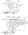
- Fig.1 is a block diagram of a chroma signal decimation filter device showing a first embodiment of the present invention. Illustrated in Fig.1 are an input chrominance signal 1, an input luminance signal 2, a correlation detector 3 for calculating a correlation between two data of the input luminance signal 3, a correlation signal 4, a filter selector 5 for selecting a filter to be used, a filter selecting signal 6 for activating the filter selected by the filter selector 5, and a filter unit 7 for filtering the input chrominance signal 1.
- the filter unit 7 comprises a couple of filters 10a and 10b for filtering the input chrominance signal 1 and a selector switch 11 for connecting one of the two filters 10a and 10b of which output is delivered as an output signal 8.
- the operation of the chroma signal decimation filter device of the first embodiment having the foregoing arrangement will now be described.
- the input luminance signal 2 is fed to the correlation detector 3 where a correlation between pixel data is calculated. If the correlation is high, the input luminance signal 2 is relatively flat. If it is low, the image data represents a sharp edge or outline pattern of picture.
- the chrominance signal is closely related to the luminance signal and if the luminance signal contains a sharp edge or outline image data, there is high probability that similar data of chrominance signal is in the same position on a screen.
- the filter selector 5 is hence actuated to select either the filter 10a for improving the quality of a flat pattern or the filter 10b for improving the quality of a sharp edge or outline pattern. More particularly, if the correlation is high, the filter 10a is selected by the action of the selector switch 11 for filtering the input chrominance signal 1 and if low, the filter 10b is selected.
- the filter unit 7 containing the two filters 10a and 10b and the selector switch 11 is controlled by the filter selector 5 for activating appropriate one of the filters 10a and 10b in correspondence to the image data carried in the input signal, thus minimizing a distortion in the picture quality which is inherent in a conventional chroma signal decimation filter device.
- Fig.2 is a block diagram of a chroma signal decimation filter device showing a second embodiment of the present invention, in which a correlation detector 3 and a filter selector 5 are identical in the arrangement to those of the first embodiment shown in Fig.1 while a filter unit 7 is different.
- the filter unit 7 comprises two delayers 20a and 20b for producing delay of an input chrominance signal 1, a ROM 21 arranged for delivering three different outputs 22a, 22b, and 22c on receiving an output signal 6 of the filter selector 5, three multipliers 23a, 23b, and 23c for multiplication of the input signal 1 by the output 22a, a delay signal of the delayer 20a by the output 22b, and a delay signal of the delayer 20b by the output 22c respectively, and an adder 25 for summing product signals 24a, 24b, and 24c of their respective multipliers 23a, 23b, and 23c to a sum signal which is in turn delivered as the filter output 8.
- the operation of the chroma signal decimation filter device of the second embodiment having the foregoing arrangement will be explained.
- the second embodiment is differed from the first embodiment shown in Fig.1 by the arrangement of the filter unit 7 in which the action of the two filters 10a and 10b and the selector switch 11 is substituted with the arithmetic operation of three different filter coefficients for producing different filter effects.
- the filter unit 7 shown in Fig.2 forms a three-tap filter associated with the three filter coefficients 22a, 22b, and 22c.
- the filter coefficients 22a, 22b, and 22c are derived from three discrete address data of the ROM 21 and released upon receipt of the output signal 6 of the filter selector 5.
- the sum of the three filter coefficients 22a, 22b, and 22c is 1 so that the energy of an output chrominance signal which has been filtered becomes equal to that of the input chrominance signal 1.
- the three filter coefficients 22a, 22b, and 22c of the ROM 21 are predetermined so that if the filter selector 5 detects that the luminance signal carries edge image data, they provides a filtering for improving the quality of an edge pattern and if not, a filtering for improving the quality of a flat pattern.
- the filter coefficients 22a, 22b, and 22c are multiplied by the input signal 1, the delay signal of the delayer 20a, and the delay signal of the delayer 20b respectively to the product signals 24a, 24b, and 24c.
- the product signals 24a, 24b, and 24c are then summed up by the adder 25 to the filter output 8.
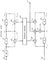
- Fig.3 is a block diagram of a line decimation filter device, another form of the chroma signal decimation filter device, showing a third embodiment of the present invention.
- an input terminal 100 for receiving a luminance signal
- a couple of 1H delayers 101 and 102 for subtracters 103 and 104 for calculating a differential between two line data
- a coefficient calculator 105 for calculating two multiplication coefficients p and q from difference signals of the subtracters 103 and 104
- an input terminal 106 for receiving a chrominance signal
- an adder 112 for summing the product signals from their respective multipliers 109, 110, and 111
- an output terminal 113 for delivering a sum signal.
- a pixel data of the chrominance signal is denoted by C i and two, upper and lower, pixel data next to the pixel data C i situated on the preceding and succeeding lines are represented by C i-1 and C i+1 respectively.
- a pixel data of the luminance signal at the same location of a screen as of the pixel C i is denoted by Y i and its adjacent two pixel data on the preceding and succeeding lines are represented by Y i-1 and Y i-1 respectively.
- the luminance signal is first examined about Y i , Y i-1 , and Y i-1 which are located at the same points as shown in Fig.4.
- the coefficients p and q are determined by the two differentials between the current line and its preceding and succeeding lines of the luminance signal as calculated using the following equations (2) and (3), in which a is a constant for preeventing the coefficients p and q from being set to extreme values when the two differentials between the lines both are small.
- the luminance signal fed from the input terminal 100 is examined by the subtracters 103 and 104 in which the differentials Y i ⁇ 1-Y i and Y i -Y i+1 between the current line and the preceding and succeeding lines are calculated respectively for output to the coefficient calculator 105.
- the coefficient calculator 105 converts the two differentials to their absolute values and calculates the multiplication coefficients p and q using the equations (2) and (3).
- the chrominance signal fed to the input terminal 106 is filtered through multiplication of C i-1 , C i , and C i+1 by p and q with their respective multipliers 109, 111, and 110 and summation of the resultant products with the adder 112 using the equation (1).
- the first case (i) exhibits no change in the luminance signal and thus, the filter device acts as a 3-tap linear phase filter of which action is equal to that of a conventional filter device and expressed by the equation (1a).
- the other two cases (ii) and (iii) indicate that the luminance signal carries edge image data and thus, the chrominance signal is filtered corresponding to the correlation between pixel data of the luminance signal. Accordingly, when the correlation between the chrominance and luminance signal data at the same pixel position is high or their respective edge patterns are precisely overlapped each other, no color fringing will appear because edge of the chrominance signal are restored.
- Fig.7 is a block diagram showing another arrangement of a coefficient calculating means in which a coefficient selector 114 is added.
- the two coefficients p and q calculated by the coefficient calculator 105 are not directly used for multiplication. They are fed to the coefficient selector 114 which is provided with a plurality of predetermined coefficient pairs.
- the coefficient selector 114 selects one coefficient pair and delivers them as a pair of given coefficients to the corresponding multipliers.
- the hardware complexity of the filter device will be facilitated with the use of a filter coefficient equal to the n-th power of 1/2.
- the third embodiment of the present invention provides an improved filtering action for line decimation of data of the chrominance signal in which if the correlation between the chrominance and luminance data is high, color fringing in the edge pattern of the chrominance signal will hardly be generated and no aliasing distortion will appear.
- Fig.8 is a block diagram of a chroma signal decimation filter device showing a fourth embodiment of the present invention. Illustrated in Fig.8 are a couple of filters 150a and 150b for filtering a luminance signal 2, output signals 151a and 151b from their respective filters 150a and 150b, two subtracters 152a and 152b, difference signals 4a and 4b from their respective subtracters 152a and 152b, a filter 10a for improving the quality of a picture which contains no edge pattern, a filter 10b for improving the quality of a picture which shows an edge pattern between two pixels, a filter 10c for improving the quality of a picture shows an edge pattern in the front, and a filter 10d for improving the quality of a picture which show an edge pattern in the rear.
- filters 150a and 150b for filtering a luminance signal 2
- output signals 151a and 151b from their respective filters 150a and 150b
- two subtracters 152a and 152b difference signals 4a and 4b from their respective
- the filters 150a and 150b are arranged for emphasizing the edge pattern in front and rear of decimated pixel data respectively.
- the edge emphasized signals 151a and 151b are fed to their respective subtracters 152a and 152b where they are subtracted from the input signal 2.
- the resultant difference signals 4a and 4b represent the magnitude of the edge pattern data. More particularly, if 4a is greater than 4b, the edge pattern exists in the front and if 4b is greater than 4a, it appears in the rear. Accordingly, a filter selector 5 determines the optimum filter from the four different cases:
- the selection of an optimum filter is conducted by detection of the edge pattern at high accuracy and thus, the quality of a reproduced picture will be improved.
- it is examined whether the edge pattern appears between pixels Y i-2 , Y i-1 , Y i , Y i+1 , and Y i+2 of the luminance signal.
- Fig.10 is a block diagram showing a correlation detector for detection of the edge pattern by the foregoing procedure. Illustrated are an luminance signal 2, four delayers 160a, 160b, 160c, and 160d for producing delay signals from the luminance signal, delay signals 161a, 161b, 161c, and 161d from their respective delayers 160a, 160b, 160c, and 160d, four subtracters 162a, 162b, 162d, and 162e, difference signals 163a, 163b, 163d, and 163e from their respective subtracters 162a, 162b, 162d, and 162e, a couple of adders 164c and 164f, two shifters 165c and 165f for multiplication by 1/2, two comparators 166a and 166b , and output signals 4a and 4b from their respective comparators 166a and 166b.
- an luminance signal 2 four delayers 160a, 160b, 160c, and 160d for producing delay signals from the luminance signal, delay signals
- the correlation detector is designed for detecting whether the edge pattern appears between Y i-2 , Y i-1 , Y i , Y i+1 , and Y i+2 of the luminance signal in order to determine an appropriate filter for decimation of pixel data about the pixel C i shown in Fig.9.
- the input luminance signal 2 is fed to a row of the delayers 160a, 160b, 160c, and 160d where delay signals are produced.
- the delay signals 161a, 161b, 161c, and 161d are Y i+1 , Y i , Y i-1 , and Y i-2 .
- the difference signals 163a, 163b, 163d, and 163e from their respective subtracters 162a, 162b, 162d, and 162e are equal to Y i+2 -Y i+1 , Y i -Y i+1 , Y i-2 -Y i-1 ,and Y i - Y i -1 respectively.
- the comparator 166b performs comparison between the absolute values of Y i+2 -Y i+1 , Y i -Y i+1 , and Y i+2 /2+Y i /2-Y i+1 and delivers the least value as an output.
- the absolute value of Y i+2 -Y i+1 is the least, it is determined that the edge pattern appears between Y i+2 and Y i+1 . If the absolute value of Y i -Y i+1 is the least, it is determined that the edge pattern appears between Y i and Y i+1 . If the absolute value of Y i+2 /2+Y i /2-Y i+1 is the least, it is determined that no edge pattern appears between Y i and Y i+2 . The resultant output of the comparator 166b is delivered as the signal 4b.
- the comparator 166a performs comparison between the absolutes values of Y i-2 -Y i-1 , Y i -Y i-1 , and Y i-2 /2+Y i /2-Y i-1 and delivers the least value as an output. More specifically, if the absolute value of Y i-2 -Y i-1 is the least, it is determined that the edge pattern appears between Y i and Y i-1 . If the absolute value of Y i -Y i-1 is the least, it is determined that the edge pattern appears between Y i-2 and Y i-1 .
- Fig.11 is a block diagram of a chroma signal interpolation filter device showing a fifth embodiment of the present invention. Illustrated in Fig.11 are an input chrominance signal 51, an input luminance signal 52, a correlation detector 53 for calculating a correlation between two data of the luminance signal 52, a correlation signal 54, a filter selector 55 for selecting a filter to be used, a filter selecting signal 56 for activating the filter selected by the filter selector 55, and a filter unit 57 for filtering the input chrominance signal 51.
- the filter unit 57 comprises a zero-value insertion unit 60 for insertion of 0 into the interpolated pixel value of the input chrominance signal 51, three filters 61a, 61b, and 61c for filtering an output signal of the zero-value insertion unit 60, and a selector switch 62 for connecting one of the three filters 61a, 61b, and 61c of which output is delivered as an output signal 58 of the filter device.
- the input luminance signal 52 is fed to the correlation detector 53 where a correlation between pixel data is calculated. If the correlation is high, the input luminance signal 52 carries an image data which exhibits a relatively flat pattern throughout the pixels. If it is low, the image data represents a sharp edge or outline pattern of picture.
- the chrominance signal is closely related to the luminance signal and if the luminance signal contains a sharp edge or outline image data, will at high probability carry similar data about the same location of a picture screen.
- the filter selector 55 is hence actuated to select through the action of the selector switch 62 one of the three filters 61a, 61b, and 61c for optimum filtering of the input chrominance signal 51. More particularly, if the correlation is high, the filter 61a is selected for performing ultimate interpolation on a flat pattern. If it is low, either the filter 61b or 61c is selected depending on the location (in the front or rear) of an edge pattern. For filtering both the interpolated pixel data and the pixel data to be used for interpolation of the input chrominance signal 51 at an equal level, a zero-value insertion unit 60 is provided for presetting the interpolated data value to 0.
- the filter unit 57 containing the three filters 61a, 61b, and 61c and the selector switch 62 is controlled by the filter selector 55 for activating the most favorable filter for enhancing the quality of a picture which exhibits an edge or flat pattern, thus minimizing a declination in the picture quality which is inherent in a conventional chroma signal interpolation filter device.
- Fig.12 is a block diagram of a chroma signal interpolation filter device showing a sixth embodiment of the present invention, in which a correlation detector 53 and a filter selector 55 are identical in the arrangement to those of the fifth embodiment shown in Fig.11 while a filter unit 57 is different.
- the filter unit 57 comprises two delayers 70a and 70b for producing delay of an input chrominance signal 51, a ROM 71 arranged for delivering three different outputs 72a, 72b, and 72c on receiving an output signal 56 of the filter selector 55, three multipliers 73a, 73b, and 73c for multiplication of the input signal 51 by the output 72a, a delay signal of the delayer 70a by the output 72b, and a delay signal of the delayer 70b by the output 72c respectively, and an adder 75 for summing product signals 74a, 74b, and 74c of their respective multipliers 73a, 73b, and 73c to a sum signal which is in turn delivered as the filter output 58.
- the sixth embodiment is differed from the fifth embodiment shown in Fig.11 by the arrangement of the filter unit in which the selection from the three fillers 61a, 61b, and 61c with the selector switch 62 is substituted with the arithmetic operation of three different filter coefficients for producing different filter effects.
- the filter unit 57 shown in Fig.12 forms a three-tap filter associated with the three filter coefficients 72a, 72b, and 72c.
- the filter coefficients 72a, 72b, and 72c are derived from three discrete address data of the ROM 71 and released upon receipt of the output signal 56 of the filter selector 55.
- the sum of the filter coefficients 72a and 72c is 1 and also, 72b is 1 so that the energy of an output chrominance signal which has been filtered becomes equal to that of the input chrominance signal 51.
- the three filter coefficients 72a, 72b, and 72c of the ROM 71 are predetermined so that if the filter selector 55 detects that the luminance signal carries edge image data, they provide a filtering action for enhancing the quality of an edge pattern and if not, a filtering action for enhancing the quality of a flat pattern.
- the filter coefficients 72a, 72b, and 72c are multiplied by the input signal 51, the delay signal of the delayer 70a, and the delay signal of the delayer 70b respectively to the product signals 74a, 74b, and 74c.
- the product signals 74a, 74b, and 74c are then summed up by the adder 75 to the filter output 58.
- Fig.13 is a block diagram of a line interpolation filter device, another form of the chroma signal interpolation filter device, showing a seventh embodiment of the present invention.
- an input terminal 200 for receiving a luminance signal
- a couple of 1H delayers 201 and 202 for subtracters 203 and 204 for calculating a differential between two line data
- a coefficient calculator 205 for calculating two multiplication coefficients p and q from difference signals of the subtracters 203 and 204
- an input terminal 206 for receiving a chrominance signal
- a couple of 1H delayers 207 and 208 two multipliers 209 and 210
- an adder 211 for summing the product signals from their respective multipliers 209 and 210 and the delay signal from the 1H delayer 207
- an output terminal 213 for delivering a sum signal.
- a pixel data of the chrominance signal is denoted by C i and two, upper and lower, pixel data next to the pixel C i situated on the preceding and succeeding lines are represented by C i-1 and C i+1 respectively.
- a pixel data of the luminance signal at the same location of a screen as of the pixel C i is denoted by Y i and its two adjacent pixel data on the preceding and succeeding lines are represented by Y i-1 and Y i+1 respectively.
- the interpolation filtering of the chrominance signal is executed through examining the data of Y i , Y i-1 , and Y i+1 .
- the coefficients p and q are determined by the two differentials between the current line and its preceding and succeeding lines of the luminance signal as calculated using the following equations (5) and (6), in which b is a constant provided for the same purpose as of the constant a of the equation (1).
- the luminance signal fed from the input terminal 200 is examined by the subtracters 203 and 204 in which the differentials Y i-1 -Y i and Y i -Y i+1 between the lines are calculated respectively for output to the coefficient calculator 205.
- the coefficient calculator 205 converts the two differentials to their absolute values and calculates the multiplication coefficients p and q using the equations (5) and (6).
- the chrominance signal processed by zero insertion and fed to the input terminal 206 is filtered through multiplication by p and q with the multipliers 209 and 210 and summation of the resultant products with the adder 212 using the equation (4).
- the principle of the filtering action is identical to that for the line decimated signal. Accordingly, when the correlation between the chrominance and luminance signal data at the same pixel position is high and their respective edge patterns are precisely overlapped each other, no color fringing will appear because edge components of the chrominance signal are restored.
- the determination of filter coefficients in this embodiment will also be carried out by the same procedure as depicted in Fig.7.
- the seventh embodiment of the present invention provides an improved filtering action for interpolation of the line decimated chrominance signal in which if the correlation between the chrominance and luminance data is high, color fringing in the edge pattern of the chrominance signal will hardly be generated and no aliasing distortion will appear.
- Fig.15 is a block diagram of a chroma signal interpolation filter device showing a eighth embodiment of the present invention, in which a correlation detector 53 and a filter selector 55 are identical in the arrangement to those of the fifth embodiment shown in Fig.11 while a filter unit 57 is different.
- the filter unit 57 comprises three filters 61a, 61b, and 61c for filtering the interpolated pixel value of an the input chrominance signal 51, a selector switch 62 activated by a signal 56 from the filter selector 55 for connecting one of the three filters 61a, 61b, and 61c of which output is delivered as an output signal 58 of the filter device, and a selector switch 80 for directly transmitting the other component than the interpolated pixel data of the input chrominance signal 51 to the output by switching actions which are triggered at equal intervals.
- the filter selector 55 is hence actuated to select through the action of the selector switch 62 one of the three filters 61a, 61b, and 61c for optimum filtering of the input chrominance signal 51. More particularly, if the correlation between two data is high, the filter 61a is selected for performing ultimate interpolation on a flat pattern data. If it is low, either the filter 61b or 61c is selected depending on the location of an edge pattern.
- the filtering action of the filter 61a, 61b, or 61c needs to work on the interpolated pixel component of the signal but not the other component.
- the selector switch 80 performs a periodic switching action for if the interpolated pixel data is involved, passing the output of a selected filter and if not, transmitting the input chrominance signal 51 directly across the filter unit 57.
- the number of pixel data to be filtered is decreased as compared with the fifth embodiment shown in Fig.11 and thus, the speed of the filtering action will be increased.
- the filter unit 57 containing the three filters 61a, 61b, and 61c, the selector switch 62, and the extra selector switch 80 is controlled by the filter selector 55 for activating the most favorable filter for enhancing the quality of a picture which exhibits an edge or flat pattern, thus minimizing a declination in the picture quality during the filtering action.
- Fig.16 is a block diagram of a chroma signal interpolation filter device showing a ninth embodiment of the present invention.
- another form of the correlation detector 53 of the eighth embodiment is provided comprising a couple of delayers 90 and 92 for producing two delay signals 91 and 93 respectively, two subtracters 94 and 96 for producing two difference signals 95 and 97 respectively, and an average calculator 98 for calculating an average value 99.
- the correlation detector 53 is designed for detecting whether the edge pattern exists in the front and rear of the pixel data of an input luminance signal situated at the same location of the interpolated pixel data of a chrominance signal. It is assumed that the luminance signal pixel is Y i and its preceding and succeeding pixels are Y i-1 and Y i+1 respectively. If the delay signal 91 is Y i , the input signal 52 and the delay signal 93 are Y i+1 and Y i-1 .
- the difference signals 95 and 97 from their respective subtracters 94 and 96 are equal to Y i+1 -Y i and Y i-1 -Y i respectively and the average signal 99 of the average calculator 98 is expressed as Y i+1 /2+Y i-1 /2-Y i . It is now compared between the absolute values of the signals 95, 97, and 98. If the absolute value of the signal 98 is the least, it is determined that no edge pattern is present and the interpolation on the chrominance signal is carried out using the filter 61a for enhancing the quality of a flat pattern.
- the filter 61b for enhancing the quality of the edge pattern in the front. If the absolute value of the signal 97 is the least, the interpolation is carried out with the filter 61c for enhancing the edge pattern in the rear.
- the chroma signal interpolation filter device will be simple in the hardware arrangement yet ensuring ultimate filtering capability.
- Fig.17 is a block diagram of a chroma signal interpolation filter device showing a tenth embodiment of the present invention. Illustrated are an input luminance signal 244, a delayer 245 for producing (one line -1)-pixel delay, a delay output 246 of the delayer 245, a delayer 247 for producing 1-pixel delay, a delay output 248 of the delayer 247, a subtracter 249, a difference signal 250 of the subtracter 249, a delayer 251 for producing 1-pixel delay, a delay output 252 of the delayer 251, a subtracter 253, a difference signal 254 of the subtracter 253, a subtracter 255, a difference signal 256 of the subtracter 255, a delayer 257 for producing 1-line relay, a delay output 258 of the delayer 257, a subtracter 259, a difference signal 260 of the subtracter 259, an adder 261, a sum signal 262 of the adder 261, a divider 263, a quotient
- Fig.19 is an explanatory view of interpolation in the embodiment, showing an enlargement of Fig.18.
- Y represents a pixel data of the chrominance signal to be interpolated and A, B, C, and D are existing data pixels.
- a data pixel of the luminance signal at the same location as of Y is denoted by the letter y and pixels a, b, c, and d correspond to A, B, C, and D respectively.
- the criteria for comparing action of an interpolating means is expressed as: if
- , then Y (A+B) /2, if
- , then Y (C+D) /2, if
- the input luminance signal 244 is fed to the delayer 245 where it is delayed by (one line-1)-pixel to determine the pixel d.
- the delay signal 246 is then 1-pixel delayed by the delayer 247 determining the pixel y.
- the subtracters 249 and 255 perform subtraction of the delay signal 246 and the input luminance signal 244 from the delay signal 248 respectively thus producing (y-d) and (y-b).
- the difference signal 250 is 1-pixel delayed by the delayer 251 to the delay signal 252 which is then subtracted from the difference signal 250 at the subtracter 253.
- the difference signal 254 is (2y-c-d) equivalent to 2(y-y2).
- the difference signal 256 is 1-line-pixel delayed by the delayer 257 to the delay signal 258 which is then subtracted from the difference signal 256 at the subtracter 259.
- the difference signal 260 is 2(y-y1).
- the two difference signals 254 and 260 are summed up by the adder 261 to the sum signal 262 which is then divided by two at the divider 263 to the quotient signal 264 equal to 2(y-y3).
- the absolute values of the difference signals 254 and 260 and the quotient signal 264 are compared from one another by the comparator 265 which in turn delivers the comparison signal 266 instructing a desired interpolation procedure by which the absolute value is minimized.
- the input chrominance signal 267 is fed to the delayer 268 where it is delayed by (one line-1)-pixel to the delay signal 269.
- the delay signal 269 is further 2-pixel delayed by the delayer 270 to the delay signal 271.
- the two delay signals 269 and 271 are summed by the adder 272 to the sum signal 273 equal to (C+D).
- the delay signal 271 is (one line-1)-pixel delayer by the delayer 274 to the delay signal 275 which is then summed with the input chrominance signal 267 by the adder 276 to the sum signal 277 equal to (A+B).
- the two sum signals 273 and 277 are summed up by the adder 278 to the sum signal 279 which is in turn divided by two at the divider 280 to the quotient signal 281 equivalent to (A+B+C+D)/2.
- the selector 282 selects one from the two sum signals 273 and 277 and the quotient signal 281 which corresponds to the interpolating means determined by the comparison signal 266 and then delivers it as the chrominance interpolation signal 283. It is noted that the output of the chroma signal interpolation filter device of this embodiment is not normalized and hence, should be multiplied by 1/2 at either the input or output end of the device.
- each embodiment of the present invention allows the chrominance signal to be interpolated by three discrete, vertical, horizontal, and planar, interpolation techniques so that a reproduced image of interpolated data can be enhanced in the quality with the use of a relatively simple hardware arrangement.
- FIG.20 is a block diagram showing the decimation of horizontal pixel data according to the present invention, in which there are provided a lowpass filter 120 for decimation of data and four 1-pixel delayers 121, 122, 123, and 124.
- the luminance signal is sampled by frequencies of a multiple of an integer of the chrominance signal and the number of its samples in each horizontal scanning period becomes n times (n is an integer) that of the chrominance signal.
- the luminance signal is sampled by a frequency two time greater than that of the chrominance signal, the number of samples is two times that of the chrominance signal. Simultaneously, its frequency bandwidth for transmission is also doubled.
- the luminance signal having such a two-time bandwidth is correlation detected, its aliasing component causes erratic filtering of the chrominance signal. Accordingly, the bandwidth of the luminance signal is reduced to 1/2 by the lowpass filter 120 prior to the data decimation and filter coefficients for decimation of the chrominance signal is determined by detecting a correlation between pixel data of the luminance signal which correspond those of the chrominance signal in the respect of position and bandwidth.
- Fig.21 is a block diagram showing the interpolation of horizontal pixel data according to the present invention, in which there are provided a lowpass filter 220 for data interpolation and four 1-pixel delayers 221, 222, 223, and 224.
- the processing of the luminance signal by the arrangement shown in Fig.21 is similar to that of the data decimation. More particularly, the luminance signal is bandlimit filtered and interpolated by the lowpass 220 filter and a correlation between two data thereof is detected for calculating filter coefficients for interpolation of the chrominance signal.
- Both the chroma signal decimation filter device and the chroma signal interpolation device of the present invention are almost identical in the arrangement and can commonly be used for decimation and interpolation by shifting their filter coefficients from decimation values to interpolation values or vice versa.
- the correlation values p and q and the decimation or interpolation coefficients for C i shown in Figs.3 and 13 may be varied for desired filtering action without changing the arrangement of components.
- the number of filter taps and the setting of coefficients are not limited to the embodiments of the present invention which are only illustrative. They will arbitrarily be determined in respect to the accuracy of filtering action and the feasibility of hardware.
Landscapes
- Engineering & Computer Science (AREA)
- Multimedia (AREA)
- Signal Processing (AREA)
- Processing Of Color Television Signals (AREA)
- Color Television Systems (AREA)
Abstract
Description
- The present invention relates to a chroma signal decimation filter device for removing sampled data from the chrominance component of a digital video signal and a chroma signal interpolation filter device for interpolating the sampled data with the use of their adjacent data.
- For reducing the data of a video signal to a desired size for ease of recording or transmission, a method of decimation of horizontal or vertical sample data of the signal is commonly employed. While the signal for recording or transmission is decreased in the amount of data, its frequency band to be reproduced is less than a particular (or Nyquist) frequency which has a wavelength two times the sampling period. If the frequency band before sampling exceeds the Nyquist frequency, aliasing distortion will appear declining the quality of a reproduced image. The Nyquist theorem suggests that the sampled data dropped by decimation will be restored through filtering them to pass only a Nyquist bandwidth portion.
- The aliasing distortion is undesired in visual reproduction and intended to be eliminated by reducing prior to data decimation the bandwidth of a signal to less than the Nyquist frequency with a lowpass filter in a conventional signal decimation device. For interpolation of a data portion below the Nyquist frequency, the same lowpass filter for limiting a bandwidth to less than the Nyquist frequency can be used. More specifically, all the frequency components below the Nyquist frequency can be decoded with the LPF which is thus desirable for use as an interpolation device.
- It is known that the visual sensitivity of human eyes is not high to a chrominance signal as compared with to a luminance signal and also, high frequency components are less sensitive than low frequency components. Accordingly, the technique of decimating the chrominance components is preferred for reducing the data quantity of a video signal. Such devices for limiting the band of the chrominance components to a suitable width for decimation and interpolation are known as a chroma signal decimation filter device and a chroma signal interpolation filter device.
- However, known chroma signal decimation and interpolation filter devices are not capable, never in theory, of reproducing a frequency band more than the Nyquist frequency. For example, an image data which contains an elaborate picture pattern of colors can be processed by the known chroma signal decimation and interpolation filter devices with the development of undesired color fringing.
- It is an object of the present invention to provide a chroma signal decimation filter device and a chroma signal interpolation filter device which both can reproduce a band of frequencies of a video signal more than a level determined by the Nyquist frequency without development of aliasing distortion after the decimation and interpolation of chrominance data.
- For achievement of the above object, a chroma signal decimation filter device according to the present invention comprises: a correlation detector for detecting a correlation between pixel data of a luminance signal which correspond in a positional assignment on a picture screen to those of a chrominance signal; a filter unit for performing at least two different filterings using a target pixel data and its adjacent pixel data of the chrominance signal; and a filter selector for determining the filtering procedure of the filter unit in accordance with the correlation between the pixel data of the luminance signal detected by the correlation detector.
- Also, a chroma signal interpolation filter device according to the present invention comprises: a correlation detector for detecting a correlation between pixel data of a luminance signal which correspond in the positional assignment on a picture screen to those of a chrominance signal, one of which is a target pixel data to be interpolated and has a value of 0; a filter unit for performing a filtering using some other chrominance pixel data than the target pixel data to be interpolated; and a filter selector for determining filter coefficients of the filter unit in accordance with the correlation between the pixel data of the luminance signal detected by the correlation detector.
- Another chroma signal interpolation filter device according to the present invention is provided comprising: a correlation detector for detecting a correlation between pixel data of a luminance signal which correspond to those of a chrominance signal, one of which is a target pixel data to be interpolated, in the positional assignment on a screen; a filter unit for performing at least two different filterings on the target pixel data to be interpolated using some other chrominance pixel data than the target pixel data while no filtering the other pixel data of the chrominance signal; and a filter selector for determining the filtering procedure of the filter unit in accordance with the correlation between the pixel data of the luminance signal detected by the correlation detector.
- As understood from the description of the prior art, the aliasing distortion which is unwanted in visual display will appear with the Nyquist thoerem if the filtering for limiting a frequency band in accordance is not carried out during the decimation and interpolation of chrominance data. Also, a conventional hardware arrangement designed for performing the foregoing filtering with the Nyquist theorem is large in the size whereby aliasing distortion will hardly be avoided. In particular, the aliasing distortion tends to appear in the form of color fringing at the edge and outline regions of a reproduced picture and if worse, the filtering itself will cause more error in a particular video signal than the aliasing distortion thus declining the quality of the picture.
- In common, the chrominance component of a video signal is closely related with the luminance component and its edge or outline pattern of picture will appear at the same location on a screen as of the luminance signal. Accordingly, declination in the picture quality during the decimation and interpolation of the chrominance components can be prevented by detecting the location of an edge or outline portion from the luminance components which is neither decimated nor interpolated and filtering the edge or outline pattern data with a filter which provides less color fringing and the remaining data with another filter which provides less aliasing distortion.
- In operation of the chroma signal decimation and interpolation filter devices of the present invention, the correlation detector is actuated for calculating a correlation between pixel data of the luminance component. For example, if the correlation calculated by the correlation detector is low, it is determined that an edge or outline pattern data is carried. Then, the filter selector actuates the filter unit to select a filter which provides less color fringing. Otherwise, a filter which provides less aliasing distortion will be selected. Also, more than two types of filters may be provided for corresponding to the location of an edge pattern and the magnitude of a correlation. With the use of the foregoing improved arrangement, the quality of a reproduced image will be much improved as compared with a conventional arrangement employing a stationary Nyquist filter.
-
- Fig.1 is a block diagram of a chroma signal decimation filter device showing a first embodiment of the present invention;
- Fig.2 is a block diagram of a chroma signal decimation filter device showing a second embodiment of the present invention;
- Fig.3 is a block diagram of a chroma signal decimation filter device showing a third embodiment of the present invention;
- Fig.4 is an explanatory illustration showing the pixel data arrangement of both a chrominance signal and a luminance signal;
- Fig.5 is an explanatory illustration showing variations in the luminance signal;
- Fig.6 is an explanatory illustration showing a filter output of the chrominance signal which contains an edge pattern data;
- Fig.7 is a block diagram showing an arrangement of a coefficient selector means;
- Fig.8 is a block diagram of a chroma signal decimation filter device showing a fourth embodiment of the present invention;
- Fig.9 is an explanatory illustration showing the pixel data arrangement of both a chrominance signal and a luminance signal;
- Fig.10 is a block diagram showing an arrangement of a correlation detector;
- Fig.11 is a block diagram of a chroma signal interpolation filter device showing a fifth embodiment of the present invention;
- Fig.12 is a block diagram of a chroma signal interpolation filter device showing a sixth embodiment of the present invention;
- Fig.13 is a block diagram of a chroma signal interpolation filter device showing a seventh embodiment of the present invention;
- Fig.14 is an explanatory illustration showing the pixel data arrangement of both a chrominance signal and a luminance signal;
- Fig.15 is a block diagram of a chroma signal interpolation filter device showing a eighth embodiment of the present invention;
- Fig.16 is a block diagram of a chroma signal interpolation filter device showing a ninth embodiment of the present invention;
- Fig.17 is a block diagram of a chroma signal interpolation filter device showing a tenth embodiment of the present invention;
- Fig.18 is an explanatory illustration showing the pixel data arrangement of a chrominance signal;
- Fig.19 is an explanatory illustration showing the pixel data arrangement of both a chrominance signal and a luminance signal;
- Fig.20 is a block diagram of the chroma signal decimation filter device of the third embodiment for decimation of horizontal data; and
- Fig.21 is a block diagram of the chroma signal decimation filter device of the seventh embodiment for interpolation of horizontal data.
- Fig.1 is a block diagram of a chroma signal decimation filter device showing a first embodiment of the present invention. Illustrated in Fig.1 are an
input chrominance signal 1, aninput luminance signal 2, acorrelation detector 3 for calculating a correlation between two data of theinput luminance signal 3, acorrelation signal 4, afilter selector 5 for selecting a filter to be used, afilter selecting signal 6 for activating the filter selected by thefilter selector 5, and afilter unit 7 for filtering theinput chrominance signal 1. Thefilter unit 7 comprises a couple offilters input chrominance signal 1 and aselector switch 11 for connecting one of the twofilters output signal 8. - The operation of the chroma signal decimation filter device of the first embodiment having the foregoing arrangement will now be described. The
input luminance signal 2 is fed to thecorrelation detector 3 where a correlation between pixel data is calculated. If the correlation is high, theinput luminance signal 2 is relatively flat. If it is low, the image data represents a sharp edge or outline pattern of picture. The chrominance signal is closely related to the luminance signal and if the luminance signal contains a sharp edge or outline image data, there is high probability that similar data of chrominance signal is in the same position on a screen. In operation, thefilter selector 5 is hence actuated to select either thefilter 10a for improving the quality of a flat pattern or thefilter 10b for improving the quality of a sharp edge or outline pattern. More particularly, if the correlation is high, thefilter 10a is selected by the action of theselector switch 11 for filtering theinput chrominance signal 1 and if low, thefilter 10b is selected. - As understood, the
filter unit 7 containing the twofilters selector switch 11 is controlled by thefilter selector 5 for activating appropriate one of thefilters - Fig.2 is a block diagram of a chroma signal decimation filter device showing a second embodiment of the present invention, in which a
correlation detector 3 and afilter selector 5 are identical in the arrangement to those of the first embodiment shown in Fig.1 while afilter unit 7 is different. Thefilter unit 7 comprises twodelayers input chrominance signal 1, aROM 21 arranged for delivering threedifferent outputs output signal 6 of thefilter selector 5, threemultipliers input signal 1 by theoutput 22a, a delay signal of thedelayer 20a by theoutput 22b, and a delay signal of thedelayer 20b by theoutput 22c respectively, and anadder 25 for summingproduct signals respective multipliers filter output 8. - The operation of the chroma signal decimation filter device of the second embodiment having the foregoing arrangement will be explained. The second embodiment is differed from the first embodiment shown in Fig.1 by the arrangement of the
filter unit 7 in which the action of the twofilters selector switch 11 is substituted with the arithmetic operation of three different filter coefficients for producing different filter effects. Thefilter unit 7 shown in Fig.2 forms a three-tap filter associated with the threefilter coefficients filter coefficients ROM 21 and released upon receipt of theoutput signal 6 of thefilter selector 5. It is understood that the sum of the threefilter coefficients input chrominance signal 1. Also, the threefilter coefficients ROM 21 are predetermined so that if thefilter selector 5 detects that the luminance signal carries edge image data, they provides a filtering for improving the quality of an edge pattern and if not, a filtering for improving the quality of a flat pattern. Thefilter coefficients input signal 1, the delay signal of thedelayer 20a, and the delay signal of thedelayer 20b respectively to theproduct signals adder 25 to thefilter output 8. - Fig.3 is a block diagram of a line decimation filter device, another form of the chroma signal decimation filter device, showing a third embodiment of the present invention. As shown, there are provided an
input terminal 100 for receiving a luminance signal, a couple of 1H delayers 101 and 102, twosubtracters coefficient calculator 105 for calculating two multiplication coefficients p and q from difference signals of thesubtracters input terminal 106 for receiving a chrominance signal, a couple of 1H delayers 107 and 108, threemultipliers adder 112 for summing the product signals from theirrespective multipliers output terminal 113 for delivering a sum signal. The operation of the above arrangement will be explained. - It is assumed that a pixel data of the chrominance signal is denoted by Ci and two, upper and lower, pixel data next to the pixel data Ci situated on the preceding and succeeding lines are represented by Ci-1 and Ci+1 respectively. Similarly, a pixel data of the luminance signal at the same location of a screen as of the pixel Ci is denoted by Yi and its adjacent two pixel data on the preceding and succeeding lines are represented by Yi-1 and Yi-1 respectively. For filtering the pixel data Ci, Ci-1, and Ci-1 of the chrominance signal, the luminance signal is first examined about Yi, Yi-1, and Yi-1 which are located at the same points as shown in Fig.4. More specifically, the filtering of Ci is expressed by:


- As shown in Fig.3, the luminance signal fed from the
input terminal 100 is examined by thesubtracters coefficient calculator 105. Thecoefficient calculator 105 converts the two differentials to their absolute values and calculates the multiplication coefficients p and q using the equations (2) and (3). Meanwhile, the chrominance signal fed to theinput terminal 106 is filtered through multiplication of Ci-1, Ci, and Ci+1 by p and q with theirrespective multipliers adder 112 using the equation (1). - For description in more detail of operation of the equations (1), (2), and (3), three cases with variations in the luminance signal are assumed as shown in Fig.5. The three cases are expressed, using the equation (1), by:


- The first case (i) exhibits no change in the luminance signal and thus, the filter device acts as a 3-tap linear phase filter of which action is equal to that of a conventional filter device and expressed by the equation (1a). The other two cases (ii) and (iii) indicate that the luminance signal carries edge image data and thus, the chrominance signal is filtered corresponding to the correlation between pixel data of the luminance signal. Accordingly, when the correlation between the chrominance and luminance signal data at the same pixel position is high or their respective edge patterns are precisely overlapped each other, no color fringing will appear because edge of the chrominance signal are restored. It is now understood that the present invention is not limited to the foregoing three cases in which variations in the luminance signal are great and its filtering action corresponding to the correlation between pixel data of the luminance signal will with equal success be performed at any other case using the equations (1), (2), and (3).
- Fig.7 is a block diagram showing another arrangement of a coefficient calculating means in which a
coefficient selector 114 is added. In particular, the two coefficients p and q calculated by thecoefficient calculator 105 are not directly used for multiplication. They are fed to thecoefficient selector 114 which is provided with a plurality of predetermined coefficient pairs. In accordance with p and q, thecoefficient selector 114 selects one coefficient pair and delivers them as a pair of given coefficients to the corresponding multipliers. As the result, the hardware complexity of the filter device will be facilitated with the use of a filter coefficient equal to the n-th power of 1/2. - As set forth above, the third embodiment of the present invention provides an improved filtering action for line decimation of data of the chrominance signal in which if the correlation between the chrominance and luminance data is high, color fringing in the edge pattern of the chrominance signal will hardly be generated and no aliasing distortion will appear.
- Fig.8 is a block diagram of a chroma signal decimation filter device showing a fourth embodiment of the present invention. Illustrated in Fig.8 are a couple of
filters luminance signal 2,output signals respective filters subtracters respective subtracters filter 10a for improving the quality of a picture which contains no edge pattern, afilter 10b for improving the quality of a picture which shows an edge pattern between two pixels, afilter 10c for improving the quality of a picture shows an edge pattern in the front, and afilter 10d for improving the quality of a picture which show an edge pattern in the rear. - The operation of the above fourth embodiment will be described. The
filters signals respective subtracters input signal 2. The resultant difference signals 4a and 4b represent the magnitude of the edge pattern data. More particularly, if 4a is greater than 4b, the edge pattern exists in the front and if 4b is greater than 4a, it appears in the rear. Accordingly, afilter selector 5 determines the optimum filter from the four different cases: - (i) no edge-is present;
- (ii) two edge patterns in both the front and rear;
- (iii) edge pattern appears in the front; and
- (iv) edge pattern in the rear.
- A procedure of edge pattern detection will now be explained. As best shown in Fig.9, white dots represent pixel data to be decimated and black dots are pixel data not to be decimated. It is assumed that the filtering action is executed about the pixel Ci. In an interpolation filter device, both Ci-1 and Ci+1 are interpolated between Ci-2 and Ci and Ci and Ci+2 respectively. Accordingly, during the filtering action, it is examined not only whether the edge pattern appears on both the sides of Ci but also whether the edge pattern appears between Ci-2 and Ci-1 and between Ci+1 and Ci+2. As the result, the selection of an optimum filter is conducted by detection of the edge pattern at high accuracy and thus, the quality of a reproduced picture will be improved. In other words, it is examined whether the edge pattern appears between pixels Yi-2 , Yi-1 , Yi , Yi+1 , and Yi+2 of the luminance signal.
- Fig.10 is a block diagram showing a correlation detector for detection of the edge pattern by the foregoing procedure. Illustrated are an
luminance signal 2, fourdelayers delay signals respective delayers subtracters adders 164c and 164f, two shifters 165c and 165f for multiplication by 1/2, twocomparators 166a and 166b , andoutput signals 4a and 4b from theirrespective comparators 166a and 166b. - The operation of the correlation detector having the above arrangement will be explained. The correlation detector is designed for detecting whether the edge pattern appears between Yi-2 , Yi-1 , Yi , Yi+1 , and Yi+2 of the luminance signal in order to determine an appropriate filter for decimation of pixel data about the pixel Ci shown in Fig.9. The
input luminance signal 2 is fed to a row of the delayers 160a, 160b, 160c, and 160d where delay signals are produced. If theinput luminance signal 2 is Yi+2 , the delay signals 161a, 161b, 161c, and 161d are Yi+1 , Yi , Yi-1 , and Yi-2. Hence, the difference signals 163a, 163b, 163d, and 163e from their respective subtracters 162a, 162b, 162d, and 162e are equal to Yi+2-Yi+1 , Yi-Yi+1 , Yi-2-Yi-1 ,and Yi - Yi-1 respectively. They are then summed by theadders 164c and 164f to two sum signals which are in turn multiplied by 1/2 with the multipliers 165c and 165f respectively. Thus, the output signals of their respective multipliers 165c and 165f become Yi+2/2+Yi/2-Yi+1 and Yi-2/2+Yi/2-Yi-1. Thecomparator 166b performs comparison between the absolute values of Yi+2-Yi+1, Yi-Yi+1, and Yi+2/2+Yi/2-Yi+1 and delivers the least value as an output. In more particular, if the absolute value of Yi+2 -Yi+1 is the least, it is determined that the edge pattern appears between Yi+2 and Yi+1. If the absolute value of Yi-Yi+1 is the least, it is determined that the edge pattern appears between Yi and Yi+1. If the absolute value of Yi+2/2+Yi/2-Yi+1 is the least, it is determined that no edge pattern appears between Yi and Yi+2. The resultant output of thecomparator 166b is delivered as thesignal 4b. Similarly, the comparator 166a performs comparison between the absolutes values of Yi-2-Yi-1, Yi-Yi-1, and Yi-2/2+Yi/2-Yi-1 and delivers the least value as an output. More specifically, if the absolute value of Yi-2-Yi-1 is the least, it is determined that the edge pattern appears between Yi and Yi-1. If the absolute value of Yi-Yi-1 is the least, it is determined that the edge pattern appears between Yi-2 and Yi-1. If the absolute value of Yi-2 /2+Yi/2-Yi-1 is the least, it is determined that no edge pattern appears between Yi and Yi-2. The resultant output of the comparator 166a is delivered as the signal 4a. In this manner, the existence of an edge pattern about the pixel Yi can be detected. - Fig.11 is a block diagram of a chroma signal interpolation filter device showing a fifth embodiment of the present invention. Illustrated in Fig.11 are an
input chrominance signal 51, aninput luminance signal 52, acorrelation detector 53 for calculating a correlation between two data of theluminance signal 52, acorrelation signal 54, afilter selector 55 for selecting a filter to be used, afilter selecting signal 56 for activating the filter selected by thefilter selector 55, and afilter unit 57 for filtering theinput chrominance signal 51. Thefilter unit 57 comprises a zero-value insertion unit 60 for insertion of 0 into the interpolated pixel value of theinput chrominance signal 51, threefilters value insertion unit 60, and aselector switch 62 for connecting one of the threefilters output signal 58 of the filter device. - The operation of the chroma signal interpolation filter device of the fifth embodiment having the foregoing arrangement will now be described. The
input luminance signal 52 is fed to thecorrelation detector 53 where a correlation between pixel data is calculated. If the correlation is high, theinput luminance signal 52 carries an image data which exhibits a relatively flat pattern throughout the pixels. If it is low, the image data represents a sharp edge or outline pattern of picture. The chrominance signal is closely related to the luminance signal and if the luminance signal contains a sharp edge or outline image data, will at high probability carry similar data about the same location of a picture screen. In operation, thefilter selector 55 is hence actuated to select through the action of theselector switch 62 one of the threefilters input chrominance signal 51. More particularly, if the correlation is high, thefilter 61a is selected for performing ultimate interpolation on a flat pattern. If it is low, either thefilter input chrominance signal 51 at an equal level, a zero-value insertion unit 60 is provided for presetting the interpolated data value to 0. - As understood, the
filter unit 57 containing the threefilters selector switch 62 is controlled by thefilter selector 55 for activating the most favorable filter for enhancing the quality of a picture which exhibits an edge or flat pattern, thus minimizing a declination in the picture quality which is inherent in a conventional chroma signal interpolation filter device. - Fig.12 is a block diagram of a chroma signal interpolation filter device showing a sixth embodiment of the present invention, in which a
correlation detector 53 and afilter selector 55 are identical in the arrangement to those of the fifth embodiment shown in Fig.11 while afilter unit 57 is different. Thefilter unit 57 comprises twodelayers input chrominance signal 51, aROM 71 arranged for delivering threedifferent outputs output signal 56 of thefilter selector 55, threemultipliers input signal 51 by theoutput 72a, a delay signal of thedelayer 70a by theoutput 72b, and a delay signal of thedelayer 70b by theoutput 72c respectively, and anadder 75 for summingproduct signals respective multipliers filter output 58. - The operation of the chroma signal interpolation filter device of the sixth embodiment having the foregoing arrangement will be explained. The sixth embodiment is differed from the fifth embodiment shown in Fig.11 by the arrangement of the filter unit in which the selection from the three
fillers selector switch 62 is substituted with the arithmetic operation of three different filter coefficients for producing different filter effects. Thefilter unit 57 shown in Fig.12 forms a three-tap filter associated with the threefilter coefficients filter coefficients ROM 71 and released upon receipt of theoutput signal 56 of thefilter selector 55. It is understood that the sum of thefilter coefficients input chrominance signal 51. Also, the threefilter coefficients ROM 71 are predetermined so that if thefilter selector 55 detects that the luminance signal carries edge image data, they provide a filtering action for enhancing the quality of an edge pattern and if not, a filtering action for enhancing the quality of a flat pattern. Thefilter coefficients input signal 51, the delay signal of thedelayer 70a, and the delay signal of thedelayer 70b respectively to theproduct signals adder 75 to thefilter output 58. - Fig.13 is a block diagram of a line interpolation filter device, another form of the chroma signal interpolation filter device, showing a seventh embodiment of the present invention. As shown, there are provided an
input terminal 200 for receiving a luminance signal, a couple of 1H delayers 201 and 202, twosubtracters coefficient calculator 205 for calculating two multiplication coefficients p and q from difference signals of thesubtracters input terminal 206 for receiving a chrominance signal, a couple of 1H delayers 207 and 208, twomultipliers respective multipliers 1H delayer 207, and anoutput terminal 213 for delivering a sum signal. The operation of the above arrangement will be explained. - It is assumed, similar to the third embodiment shown in Fig.3, that a pixel data of the chrominance signal is denoted by Ci and two, upper and lower, pixel data next to the pixel Ci situated on the preceding and succeeding lines are represented by Ci-1 and Ci+1 respectively. Equally, a pixel data of the luminance signal at the same location of a screen as of the pixel Ci is denoted by Yi and its two adjacent pixel data on the preceding and succeeding lines are represented by Yi-1 and Yi+1 respectively. The interpolation filtering of the chrominance signal is executed through examining the data of Yi , Yi-1, and Yi+1. Figs.14-a and 14-
b 5 illustrate the luminance signal and the chrominance signal respectively. More specifically, the filtering of Ci is expressed by:


- As shown in Fig.13, the luminance signal fed from the
input terminal 200 is examined by thesubtracters coefficient calculator 205. Thecoefficient calculator 205 converts the two differentials to their absolute values and calculates the multiplication coefficients p and q using the equations (5) and (6). Meanwhile, the chrominance signal processed by zero insertion and fed to theinput terminal 206 is filtered through multiplication by p and q with themultipliers adder 212 using the equation (4). - The chrominance signal fed from the
input terminal 206 which has been processed by line decimation is now interpolated with 0s at the pixel points on each decimated line. More particularly, this action is expressed as, using the equation (4):

- As set forth above, the seventh embodiment of the present invention provides an improved filtering action for interpolation of the line decimated chrominance signal in which if the correlation between the chrominance and luminance data is high, color fringing in the edge pattern of the chrominance signal will hardly be generated and no aliasing distortion will appear.
- Fig.15 is a block diagram of a chroma signal interpolation filter device showing a eighth embodiment of the present invention, in which a
correlation detector 53 and afilter selector 55 are identical in the arrangement to those of the fifth embodiment shown in Fig.11 while afilter unit 57 is different. Thefilter unit 57 comprises threefilters input chrominance signal 51, aselector switch 62 activated by asignal 56 from thefilter selector 55 for connecting one of the threefilters output signal 58 of the filter device, and aselector switch 80 for directly transmitting the other component than the interpolated pixel data of theinput chrominance signal 51 to the output by switching actions which are triggered at equal intervals. - The operation of the chroma signal interpolation filter device of the eighth embodiment having the foregoing arrangement will now be described. The action of the
correlation detector 53 and thefilter selector 55 is the same as of those shown in Fig.11. In operation, thefilter selector 55 is hence actuated to select through the action of theselector switch 62 one of the threefilters input chrominance signal 51. More particularly, if the correlation between two data is high, thefilter 61a is selected for performing ultimate interpolation on a flat pattern data. If it is low, either thefilter filter selector switch 80 performs a periodic switching action for if the interpolated pixel data is involved, passing the output of a selected filter and if not, transmitting theinput chrominance signal 51 directly across thefilter unit 57. As the result, the number of pixel data to be filtered is decreased as compared with the fifth embodiment shown in Fig.11 and thus, the speed of the filtering action will be increased. - As understood, the
filter unit 57 containing the threefilters selector switch 62, and theextra selector switch 80 is controlled by thefilter selector 55 for activating the most favorable filter for enhancing the quality of a picture which exhibits an edge or flat pattern, thus minimizing a declination in the picture quality during the filtering action. - Fig.16 is a block diagram of a chroma signal interpolation filter device showing a ninth embodiment of the present invention. In the ninth embodiment, another form of the
correlation detector 53 of the eighth embodiment is provided comprising a couple ofdelayers delay signals subtracters average calculator 98 for calculating anaverage value 99. - The operation of the chroma signal interpolation filter device of the ninth embodiment having the above arrangement will be explained. The
correlation detector 53 is designed for detecting whether the edge pattern exists in the front and rear of the pixel data of an input luminance signal situated at the same location of the interpolated pixel data of a chrominance signal. It is assumed that the luminance signal pixel is Yi and its preceding and succeeding pixels are Yi-1 and Yi+1 respectively. If thedelay signal 91 is Yi, theinput signal 52 and thedelay signal 93 are Yi+1 and Yi-1 . Hence the difference signals 95 and 97 from theirrespective subtracters average signal 99 of theaverage calculator 98 is expressed as Yi+1/2+Yi-1 /2-Yi. It is now compared between the absolute values of thesignals signal 98 is the least, it is determined that no edge pattern is present and the interpolation on the chrominance signal is carried out using thefilter 61a for enhancing the quality of a flat pattern. If the absolute value of thesignal 95 is the least, it is determined that the edge pattern appears between Yi and Yi-1 and the interpolation is conducted with thefilter 61b for enhancing the quality of the edge pattern in the front. If the absolute value of thesignal 97 is the least, the interpolation is carried out with thefilter 61c for enhancing the edge pattern in the rear. - With the use of the foregoing correlation detector, the chroma signal interpolation filter device will be simple in the hardware arrangement yet ensuring ultimate filtering capability.
- Fig.17 is a block diagram of a chroma signal interpolation filter device showing a tenth embodiment of the present invention. Illustrated are an input luminance signal 244, a delayer 245 for producing (one line -1)-pixel delay, a delay output 246 of the delayer 245, a delayer 247 for producing 1-pixel delay, a delay output 248 of the delayer 247, a subtracter 249, a difference signal 250 of the subtracter 249, a delayer 251 for producing 1-pixel delay, a delay output 252 of the delayer 251, a subtracter 253, a difference signal 254 of the subtracter 253, a subtracter 255, a difference signal 256 of the subtracter 255, a delayer 257 for producing 1-line relay, a delay output 258 of the delayer 257, a subtracter 259, a difference signal 260 of the subtracter 259, an adder 261, a sum signal 262 of the adder 261, a divider 263, a quotient signal 264 of the divider 263, a comparator 265 for comparison between the difference signal 254, the difference signal 260, and the quotient signal 264, a comparison signal 266 of the comparator 265, an input chrominance signal 267, a delayer 268 for producing (one line -1)-pixel delay, a delay output 269 of the delayer 268, a delayer 270 for producing 2-pixel delay, a delay output 271 of the delayer 270, an adder 272, a sum signal 273 of the adder 272, a delayer 274 for producing (one line -1)-pixel delay, a delay signal 275 of the delayer 274, an adder 276, a sum signal 277 of the adder 276, an adder 278, a sum signal 279 of the adder 278, a divider 280, a quotient signal 281 of the divider 280, and a selector 282 for producing a chrominance interpolation signal 283 through selection of the sum signals 273 and 277 and the quotient signal 281.
- The operation of the chroma signal interpolation filter device having the foregoing arrangement will be explained. It is assumed that the pixel data of the
input chrominance signal 267 has been decimated thus forming an array of checkerboard pattern, as shown in Fig.18. The pixels denoted by the real lines remain intact while the pixels denoted by the broken lines are illuminated. This diagonal decimation technique is employed for compressing abundant data in view of the fact that visual sensitivity becomes low in the frequency characteristic of diagonal directions. Fig.19 is an explanatory view of interpolation in the embodiment, showing an enlargement of Fig.18. In Fig.19, Y represents a pixel data of the chrominance signal to be interpolated and A, B, C, and D are existing data pixels. Also, a data pixel of the luminance signal at the same location as of Y is denoted by the letter y and pixels a, b, c, and d correspond to A, B, C, and D respectively. The criteria for comparing action of an interpolating means is expressed as:
if |y-yi|≦|y-y₂| and |y-y₁|≦|y-y₃|, then Y = (A+B) /2,
if |y-y₂|≦|y-y₁| and |y-y-₂|≦|y-y₃|, then Y = (C+D) /2,
if |y-y₃|≦|y-y₁| and |y-y₃|≦|y-y₂|, then Y = (A+B+C+D) /4,
where y₁ =(a+b)/2, y₂ (c+d)/2, and y₃ (a+b+c+d)/4. - In action, the
input luminance signal 244 is fed to thedelayer 245 where it is delayed by (one line-1)-pixel to determine the pixel d. Thedelay signal 246 is then 1-pixel delayed by thedelayer 247 determining the pixel y. Thesubtracters delay signal 246 and theinput luminance signal 244 from thedelay signal 248 respectively thus producing (y-d) and (y-b). Thedifference signal 250 is 1-pixel delayed by thedelayer 251 to thedelay signal 252 which is then subtracted from thedifference signal 250 at thesubtracter 253. Hence, thedifference signal 254 is (2y-c-d) equivalent to 2(y-y₂). Similarly, thedifference signal 256 is 1-line-pixel delayed by thedelayer 257 to thedelay signal 258 which is then subtracted from thedifference signal 256 at thesubtracter 259. Hence, thedifference signal 260 is 2(y-y₁). The twodifference signals adder 261 to thesum signal 262 which is then divided by two at thedivider 263 to thequotient signal 264 equal to 2(y-y₃). The absolute values of the difference signals 254 and 260 and thequotient signal 264 are compared from one another by thecomparator 265 which in turn delivers thecomparison signal 266 instructing a desired interpolation procedure by which the absolute value is minimized. Theinput chrominance signal 267 is fed to thedelayer 268 where it is delayed by (one line-1)-pixel to thedelay signal 269. Thedelay signal 269 is further 2-pixel delayed by thedelayer 270 to thedelay signal 271. The twodelay signals adder 272 to thesum signal 273 equal to (C+D). Also, thedelay signal 271 is (one line-1)-pixel delayer by thedelayer 274 to thedelay signal 275 which is then summed with theinput chrominance signal 267 by theadder 276 to thesum signal 277 equal to (A+B). The twosum signals adder 278 to thesum signal 279 which is in turn divided by two at thedivider 280 to thequotient signal 281 equivalent to (A+B+C+D)/2. Theselector 282 selects one from the twosum signals quotient signal 281 which corresponds to the interpolating means determined by thecomparison signal 266 and then delivers it as thechrominance interpolation signal 283. It is noted that the output of the chroma signal interpolation filter device of this embodiment is not normalized and hence, should be multiplied by 1/2 at either the input or output end of the device. - As set forth above, each embodiment of the present invention allows the chrominance signal to be interpolated by three discrete, vertical, horizontal, and planar, interpolation techniques so that a reproduced image of interpolated data can be enhanced in the quality with the use of a relatively simple hardware arrangement.
- Although the embodiments shown in Figs.3 and 13 illustrate decimation and interpolation of line data of the chrominance signal, horizontal pixel data will also be decimated or interpolated with equal success by the filter device of the present invention. Fig.20 is a block diagram showing the decimation of horizontal pixel data according to the present invention, in which there are provided a
lowpass filter 120 for decimation of data and four 1-pixel delayers lowpass filter 120 prior to the data decimation and filter coefficients for decimation of the chrominance signal is determined by detecting a correlation between pixel data of the luminance signal which correspond those of the chrominance signal in the respect of position and bandwidth. Similarly, Fig.21 is a block diagram showing the interpolation of horizontal pixel data according to the present invention, in which there are provided alowpass filter 220 for data interpolation and four 1-pixel delayers - Both the chroma signal decimation filter device and the chroma signal interpolation device of the present invention are almost identical in the arrangement and can commonly be used for decimation and interpolation by shifting their filter coefficients from decimation values to interpolation values or vice versa. For example, the correlation values p and q and the decimation or interpolation coefficients for Ci shown in Figs.3 and 13 may be varied for desired filtering action without changing the arrangement of components.
- Also, the number of filter taps and the setting of coefficients are not limited to the embodiments of the present invention which are only illustrative. They will arbitrarily be determined in respect to the accuracy of filtering action and the feasibility of hardware.
Claims (17)
- A chroma signal decimation filter device comprising:
a correlation detector for detecting a correlation between pixel data of a luminance signal which correspond in the positional assignment on a picture screen to those of a chominance signal to be decimated;
a filter unit for performing at least two different filterings using a target pixel data and its adjacent pixel data of the chrominance signal; and
a filter selector for determining the filtering procedure of the filter unit in accordance with the correlation between the pixel data of the luminance signal detected by the correlation detector. - A chroma signal decimation filter device according to Claim 1, wherein the filter unit is capable of changing filter coefficients and the filter selector is adapted for determining the values of the filter coefficients of the filter unit in accordance with the correlation between the pixel data of the luminance signal detected by the correlation detector.
- A chroma signal decimation filter device according to Claim 2, wherein if the target pixel data to be decimated and its two adjacent, front and rear, data of the chrominance signal are Ci, Ci-1, and Ci+1 respectively and two of the correlation values given by the correlation detector are p and q, the output Ci' of the filter unit is obtained from:


- A chroma signal decimation filter device according to Claim 3, wherein if the three pixel data of the luminance signal corresponding to Ci, Ci-1, and Ci+1 of the chrominance signal in the positional assignment are Yi, Yi-1 , and Yi+1 and a constant is a, p and q are respectively calculated with the filter unit from:


- A chroma signal decimation filter device according to Claim 1, wherein the correlation detector is adapted for comparing the pixel data of the luminance signal corresponding to the target pixel data of the chrominance signal with at least two pixel data produced by interpolation of the luminance signal by two different interpolation techniques and transmitting a pair of resultant comparison values to the filter selector.
- A chroma signal decimation filter device according to Claim 1, wherein the correlation detector is adapted for comparing the pixel data of the luminance signal, which corresponds to the target pixel data of the chrominance signal in the positional assignment, and its adjacent pixel data with at least two pixel data produced by interpolation of the luminance signal respectively and transmitting resultant comparison values to the filter selector
- A chroma signal decimation filter device according to Claim 1, wherein the correlation detector is adapted for detecting the correlation between two data of a luminance signal which has been band limited by a lowpass filter and the filter unit is adapted for decimation of horizontally arranged pixel data of the chrominance signal.
- A chroma signal decimation filter device according to Claim 1, wherein the filter unit is adapted for decimation of vertically arranged pixel data of the chrominance signal.
- A chroma signal interpolation filter device comprising:
a correlation detector for detecting a correlation between pixel data of a luminance signal which correspond in the positional assignment on a picture screen to those of a chrominance signal, one of which is a target pixel data to be interpolated and has a value of 0;
a filter unit for performing a filtering action using some other chrominance pixel data than the target pixel data to be interpolated; and
a filter selector for determining filter coefficients of the filter unit in accordance with the correlation between the pixel data of the luminance signal detected by the correlation detector. - A chroma signal interpolation filter device according to Claim 9, wherein if the target pixel data to be interpolated and its two adjacent, front and rear, data of the chrominance signal are Ci, Ci-1, and Ci+1 respectively and two of the correlation values given by the correlation detector are p and q, the output Ci' of the filter unit is obtained from:


- A chroma signal interpolation filter device according to Claim 10, wherein if the three pixel data of the luminance signal corresponding to Ci, Ci-1, and Ci+1 of the chrominance signal in the positional assignment are Yi, Yi-₁, and Yi+1 and a constant is b, p and q are respectively calculated with the filter unit from:


- A chroma signal interpolation filter device according to Claim 9, wherein the correlation detector is adapted for detecting the correlation between two data of a luminance signal which has been band limited by a lowpass filter and the filter unit is adapted for interpolation of horizontally arranged pixel data of the chrominance signal.
- A chroma signal interpolation filter device according to Claim 9, wherein the filter unit is adapted for interpolation of vertically arranged pixel data of the chrominance signal.
- A chroma signal interpolation filter device comprising:
a correlation detector for detecting a correlation between pixel data of a luminance signal which correspond to those of a chrominance signal, one of which is a target pixel data to be interpolated, in the positional assignment on a picture screen;
a filter unit for performing at least two different filtering actions on the target pixel data to be interpolated using some other chrominance pixel data than the target pixel data while no filtering the other pixel data of the chrominance signal; and
a filter selector for determining the filtering procedure of the filter unit in accordance with the correlation between the pixel data of the luminance signal detected by the correlation detector. - A chroma signal interpolation filter device according to Claim 14, wherein the correlation detector is adapted for comparing the pixel data of the luminance signal corresponding to the target pixel data of the chrominance signal to be interpolated with at least two pixel data produced by interpolation of the luminance signal by two different interpolation techniques and transmitting a pair of resultant comparison values to the filter selector.
- A chroma signal interpolation filter device according to Claim 15, wherein the interpolation of the luminance signal is carried out in the respect of three-front, rear, and average-different data.
- A chroma signal interpolation filter device according to Claim 14, wherein the filter unit comprises three discrete filters for interpolation of the chrominance signal having a 1/2 decimated form of checkerboard pattern; a filter for vertical interpolation, a filter for horizontal interpolation, and a filter for two-dimensional, vertical and horizontal, interpolation.
Applications Claiming Priority (4)
| Application Number | Priority Date | Filing Date | Title |
|---|---|---|---|
| JP204920/90 | 1990-08-01 | ||
| JP20492090A JP2507154B2 (en) | 1990-08-01 | 1990-08-01 | Filter device |
| JP30738690A JP2532742B2 (en) | 1990-11-13 | 1990-11-13 | Thinning filter device |
| JP307386/90 | 1990-11-13 |
Publications (3)
| Publication Number | Publication Date |
|---|---|
| EP0469892A2 true EP0469892A2 (en) | 1992-02-05 |
| EP0469892A3 EP0469892A3 (en) | 1993-08-11 |
| EP0469892B1 EP0469892B1 (en) | 1997-05-21 |
Family
ID=26514737
Family Applications (1)
| Application Number | Title | Priority Date | Filing Date |
|---|---|---|---|
| EP91307027A Expired - Lifetime EP0469892B1 (en) | 1990-08-01 | 1991-07-31 | Filter device for decimation and interpolation of chrominance components of a video signal |
Country Status (3)
| Country | Link |
|---|---|
| US (1) | US5323232A (en) |
| EP (1) | EP0469892B1 (en) |
| DE (1) | DE69126176D1 (en) |
Cited By (8)
| Publication number | Priority date | Publication date | Assignee | Title |
|---|---|---|---|---|
| EP0598184A2 (en) * | 1992-11-18 | 1994-05-25 | Kabushiki Kaisha Toshiba | Multisystem signal processing and recording/reproducing apparatus |
| US5561608A (en) * | 1992-11-18 | 1996-10-01 | Kabushiki Kaisha Toshiba | Multisystem adaptable type signal processing and recording/reproducing apparatus |
| WO1997024882A2 (en) * | 1995-12-27 | 1997-07-10 | Philips Electronics N.V. | Chrominance interpolation |
| EP0802686A2 (en) * | 1996-04-17 | 1997-10-22 | Quantel Limited | Signal processing system |
| EP0862334A2 (en) * | 1997-02-27 | 1998-09-02 | Quantel Limited | A signal processing system |
| WO2006109863A1 (en) * | 2005-04-13 | 2006-10-19 | Matsushita Electric Industrial Co., Ltd. | Resampling detection apparatus, resampling detection method, resampling apparatus, and resampling method |
| CN100464588C (en) * | 2007-01-18 | 2009-02-25 | 北京中星微电子有限公司 | Method and device of data compression |
| US7791343B2 (en) * | 2007-08-01 | 2010-09-07 | Yong Jihn Kim | Superconductor with enhanced high magnetic field properties, manufacturing method thereof, and MRI apparatus comprising the same |
Families Citing this family (17)
| Publication number | Priority date | Publication date | Assignee | Title |
|---|---|---|---|---|
| JP3651511B2 (en) * | 1996-03-22 | 2005-05-25 | 富士写真フイルム株式会社 | Digital image recording apparatus and method |
| US5953691A (en) * | 1996-10-11 | 1999-09-14 | Divicom, Inc. | Processing system with graphics data prescaling |
| KR100367831B1 (en) * | 1998-06-30 | 2003-01-10 | 주식회사 팬택앤큐리텔 | Filtering method and apparatus of chrominance signal of an image |
| US20040070704A1 (en) * | 2001-10-02 | 2004-04-15 | Lazarev Pavel I. | Multilayer plate for the fabrication of a display panel |
| US6933953B2 (en) * | 2002-04-22 | 2005-08-23 | Koninklijke Philips Electronics N.V. | Cost function to measure objective quality for sharpness enhancement functions |
| US20040161039A1 (en) * | 2003-02-14 | 2004-08-19 | Patrik Grundstrom | Methods, systems and computer program products for encoding video data including conversion from a first to a second format |
| US20050094003A1 (en) * | 2003-11-05 | 2005-05-05 | Per Thorell | Methods of processing digital image and/or video data including luminance filtering based on chrominance data and related systems and computer program products |
| US7376277B2 (en) * | 2004-06-15 | 2008-05-20 | Pegasus Imaging Corporation | Data transform for improved compression of multicomponent images |
| US7787703B2 (en) * | 2005-05-11 | 2010-08-31 | Xerox Corporation | Method and system for extending binary image data to contone image data |
| US7580569B2 (en) * | 2005-11-07 | 2009-08-25 | Xerox Corporation | Method and system for generating contone encoded binary print data streams |
| US7773254B2 (en) * | 2005-11-10 | 2010-08-10 | Xerox Corporation | Method and system for improved copy quality in a multifunction reprographic system |
| US7869093B2 (en) * | 2005-11-17 | 2011-01-11 | Xerox Corporation | Method and system for improved copy quality in a multifunction reprographic system |
| US7663782B2 (en) * | 2006-01-26 | 2010-02-16 | Xerox Corporation | System and method for high addressable binary image generation using rank ordered error diffusion on pixels within a neighborhood |
| US7742658B2 (en) * | 2006-01-26 | 2010-06-22 | Xerox Corporation | System and method for boundary artifact elimination in parallel processing of large format images |
| US20080049238A1 (en) * | 2006-08-28 | 2008-02-28 | Xerox Corporation | Method and system for automatic window classification in a digital reprographic system |
| US9460491B2 (en) * | 2008-08-25 | 2016-10-04 | Xerox Corporation | Method for binary to contone conversion with non-solid edge detection |
| KR102192674B1 (en) * | 2014-06-26 | 2020-12-17 | 삼성전자 주식회사 | Apparatus and method for processing an image |
Citations (3)
| Publication number | Priority date | Publication date | Assignee | Title |
|---|---|---|---|---|
| JPS63316990A (en) * | 1987-06-19 | 1988-12-26 | Mitsubishi Electric Corp | Luminance signal/chrominance signal separation filter corresponding to image correlation |
| EP0302500A2 (en) * | 1987-08-04 | 1989-02-08 | Victor Company Of Japan, Limited | A circuit for processing a color difference signal by utilizing the change of a luminance signal |
| EP0329976A2 (en) * | 1988-01-27 | 1989-08-30 | Communications Satellite Corporation | Multiple analogous component TV system |
Family Cites Families (4)
| Publication number | Priority date | Publication date | Assignee | Title |
|---|---|---|---|---|
| US4396937A (en) * | 1980-07-23 | 1983-08-02 | Rca Corporation | Use of a single set of steering bits in a plural channel system |
| CA1270322A (en) * | 1983-12-22 | 1990-06-12 | Kotaro Asai | Adaptive comb filter |
| US4672424A (en) * | 1985-02-14 | 1987-06-09 | Rca Corporation | Progressively scanned television system with reduced chrominance bandwidth |
| US5032910A (en) * | 1989-10-02 | 1991-07-16 | Eastman Kodak Company | Mechanism for producing interpolated color values for a sampled color image signal using a linear equation technique |
-
1991
- 1991-07-30 US US07/738,140 patent/US5323232A/en not_active Expired - Lifetime
- 1991-07-31 EP EP91307027A patent/EP0469892B1/en not_active Expired - Lifetime
- 1991-07-31 DE DE69126176T patent/DE69126176D1/en not_active Expired - Lifetime
Patent Citations (3)
| Publication number | Priority date | Publication date | Assignee | Title |
|---|---|---|---|---|
| JPS63316990A (en) * | 1987-06-19 | 1988-12-26 | Mitsubishi Electric Corp | Luminance signal/chrominance signal separation filter corresponding to image correlation |
| EP0302500A2 (en) * | 1987-08-04 | 1989-02-08 | Victor Company Of Japan, Limited | A circuit for processing a color difference signal by utilizing the change of a luminance signal |
| EP0329976A2 (en) * | 1988-01-27 | 1989-08-30 | Communications Satellite Corporation | Multiple analogous component TV system |
Non-Patent Citations (1)
| Title |
|---|
| PATENT ABSTRACTS OF JAPAN vol. 13, no. 164 (E-745)19 April 1989 & JP-A-63 316 990 ( MITSUBISHI ELECTRIC CORP. ) 26 December 1988 * |
Cited By (20)
| Publication number | Priority date | Publication date | Assignee | Title |
|---|---|---|---|---|
| US5784526A (en) * | 1992-11-18 | 1998-07-21 | Kabushiki Kaisha Toshiba | Multisystem signal processing apparatus having specific hierarchical coding |
| EP0598184A3 (en) * | 1992-11-18 | 1995-09-27 | Toshiba Kk | Multisystem signal processing and recording/reproducing apparatus. |
| US5561608A (en) * | 1992-11-18 | 1996-10-01 | Kabushiki Kaisha Toshiba | Multisystem adaptable type signal processing and recording/reproducing apparatus |
| EP0598184A2 (en) * | 1992-11-18 | 1994-05-25 | Kabushiki Kaisha Toshiba | Multisystem signal processing and recording/reproducing apparatus |
| WO1997024882A2 (en) * | 1995-12-27 | 1997-07-10 | Philips Electronics N.V. | Chrominance interpolation |
| WO1997024882A3 (en) * | 1995-12-27 | 1997-09-04 | Philips Electronics Nv | Chrominance interpolation |
| US5982455A (en) * | 1996-04-17 | 1999-11-09 | Quantel Limited | Signal processing system |
| GB2312350B (en) * | 1996-04-17 | 2000-08-30 | Quantel Ltd | A signal processing system |
| GB2312350A (en) * | 1996-04-17 | 1997-10-22 | Quantel Ltd | Colour video signal processing for image enhancement |
| EP0802686A3 (en) * | 1996-04-17 | 1999-07-21 | Quantel Limited | Signal processing system |
| EP0802686A2 (en) * | 1996-04-17 | 1997-10-22 | Quantel Limited | Signal processing system |
| GB2322753B (en) * | 1997-02-27 | 2001-05-09 | Quantel Ltd | A signal processing system |
| EP0862334A3 (en) * | 1997-02-27 | 2000-07-05 | Quantel Limited | A signal processing system |
| EP0862334A2 (en) * | 1997-02-27 | 1998-09-02 | Quantel Limited | A signal processing system |
| US6281938B1 (en) | 1997-02-27 | 2001-08-28 | Quantel Limited | Signal processing system |
| WO2006109863A1 (en) * | 2005-04-13 | 2006-10-19 | Matsushita Electric Industrial Co., Ltd. | Resampling detection apparatus, resampling detection method, resampling apparatus, and resampling method |
| US7271745B2 (en) | 2005-04-13 | 2007-09-18 | Matsushita Electric Industrial Co., Ltd. | Resampling detection apparatus, resampling detection method, resampling apparatus, and resampling method |
| CN1943242B (en) * | 2005-04-13 | 2010-12-15 | 松下电器产业株式会社 | Resampling detection apparatus, resampling detection method, resampling apparatus, and resampling method |
| CN100464588C (en) * | 2007-01-18 | 2009-02-25 | 北京中星微电子有限公司 | Method and device of data compression |
| US7791343B2 (en) * | 2007-08-01 | 2010-09-07 | Yong Jihn Kim | Superconductor with enhanced high magnetic field properties, manufacturing method thereof, and MRI apparatus comprising the same |
Also Published As
| Publication number | Publication date |
|---|---|
| EP0469892B1 (en) | 1997-05-21 |
| DE69126176D1 (en) | 1997-06-26 |
| EP0469892A3 (en) | 1993-08-11 |
| US5323232A (en) | 1994-06-21 |
Similar Documents
| Publication | Publication Date | Title |
|---|---|---|
| EP0469892B1 (en) | Filter device for decimation and interpolation of chrominance components of a video signal | |
| US4551753A (en) | Picture signal processing system including spatio-temporal filter | |
| KR100657280B1 (en) | Method and apparatus for image deinterlacing using neural networks | |
| US4965667A (en) | Method and apparatus for processing signals conveyed in sub-sampled form by way of a transmission channel or record carrier | |
| JP2537172B2 (en) | Color image input device | |
| US4733300A (en) | Contour signal correction circuit for television receiver | |
| GB2231460A (en) | Adaptive spatial interpolation of digital video signals | |
| JP5173135B2 (en) | Digital video signal processing apparatus and method for adaptive Y / C separation | |
| JPH09237335A (en) | Sampling rate conversion system using digital differential analyzer | |
| JPH1013718A (en) | Noise elimination circuit | |
| EP0862334B1 (en) | A signal processing system | |
| US20060181648A1 (en) | Digital video signal processing apparatus and method for field-based adaptive spatio-temporal Y/C separation | |
| US20060176406A1 (en) | Digital video signal processing apparatus and method for frame-based adaptive temporal and spatial Y/C separation | |
| JPH0646817B2 (en) | Video signal processor | |
| GB2202706A (en) | Video signal processing | |
| JPH0779476B2 (en) | Luminance signal Color signal separation circuit | |
| JP2532742B2 (en) | Thinning filter device | |
| JPS6345988A (en) | Circuit for separating luminance signal and chrominance signal | |
| JP3003767B2 (en) | Interpolation circuit for subsampled video signal | |
| JP2685542B2 (en) | Chroma signal processing circuit | |
| US7113226B2 (en) | Method for generating a representation of a particular signal among a plurality of signals representing lines in a display | |
| JPH1042311A (en) | Image signal processor | |
| JPH06237438A (en) | Moving picture processing circuit for muse decoder | |
| EP0624974B1 (en) | Method and system of mixing video signals | |
| KR950004652Y1 (en) | Luma/chroma separation apparatus |
Legal Events
| Date | Code | Title | Description |
|---|---|---|---|
| PUAI | Public reference made under article 153(3) epc to a published international application that has entered the european phase |
Free format text: ORIGINAL CODE: 0009012 |
|
| AK | Designated contracting states |
Kind code of ref document: A2 Designated state(s): DE FR GB NL |
|
| PUAL | Search report despatched |
Free format text: ORIGINAL CODE: 0009013 |
|
| AK | Designated contracting states |
Kind code of ref document: A3 Designated state(s): DE FR GB NL |
|
| 17P | Request for examination filed |
Effective date: 19940208 |
|
| 17Q | First examination report despatched |
Effective date: 19960122 |
|
| GRAG | Despatch of communication of intention to grant |
Free format text: ORIGINAL CODE: EPIDOS AGRA |
|
| GRAH | Despatch of communication of intention to grant a patent |
Free format text: ORIGINAL CODE: EPIDOS IGRA |
|
| GRAH | Despatch of communication of intention to grant a patent |
Free format text: ORIGINAL CODE: EPIDOS IGRA |
|
| GRAA | (expected) grant |
Free format text: ORIGINAL CODE: 0009210 |
|
| AK | Designated contracting states |
Kind code of ref document: B1 Designated state(s): DE FR GB NL |
|
| PG25 | Lapsed in a contracting state [announced via postgrant information from national office to epo] |
Ref country code: NL Free format text: LAPSE BECAUSE OF FAILURE TO SUBMIT A TRANSLATION OF THE DESCRIPTION OR TO PAY THE FEE WITHIN THE PRESCRIBED TIME-LIMIT Effective date: 19970521 Ref country code: FR Effective date: 19970521 |
|
| REF | Corresponds to: |
Ref document number: 69126176 Country of ref document: DE Date of ref document: 19970626 |
|
| PGFP | Annual fee paid to national office [announced via postgrant information from national office to epo] |
Ref country code: FR Payment date: 19970709 Year of fee payment: 7 |
|
| PGFP | Annual fee paid to national office [announced via postgrant information from national office to epo] |
Ref country code: NL Payment date: 19970731 Year of fee payment: 7 |
|
| PGFP | Annual fee paid to national office [announced via postgrant information from national office to epo] |
Ref country code: DE Payment date: 19970811 Year of fee payment: 7 |
|
| PG25 | Lapsed in a contracting state [announced via postgrant information from national office to epo] |
Ref country code: DE Effective date: 19970822 |
|
| EN | Fr: translation not filed | ||
| NLV1 | Nl: lapsed or annulled due to failure to fulfill the requirements of art. 29p and 29m of the patents act | ||
| PLBE | No opposition filed within time limit |
Free format text: ORIGINAL CODE: 0009261 |
|
| STAA | Information on the status of an ep patent application or granted ep patent |
Free format text: STATUS: NO OPPOSITION FILED WITHIN TIME LIMIT |
|
| 26N | No opposition filed | ||
| PGFP | Annual fee paid to national office [announced via postgrant information from national office to epo] |
Ref country code: GB Payment date: 20000726 Year of fee payment: 10 |
|
| PG25 | Lapsed in a contracting state [announced via postgrant information from national office to epo] |
Ref country code: GB Free format text: LAPSE BECAUSE OF NON-PAYMENT OF DUE FEES Effective date: 20010731 |
|
| GBPC | Gb: european patent ceased through non-payment of renewal fee |
Effective date: 20010731 |