EP0470867A2 - Electrochromic assembly - Google Patents
Electrochromic assembly Download PDFInfo
- Publication number
- EP0470867A2 EP0470867A2 EP91307388A EP91307388A EP0470867A2 EP 0470867 A2 EP0470867 A2 EP 0470867A2 EP 91307388 A EP91307388 A EP 91307388A EP 91307388 A EP91307388 A EP 91307388A EP 0470867 A2 EP0470867 A2 EP 0470867A2
- Authority
- EP
- European Patent Office
- Prior art keywords
- assembly
- electrochromic
- devices
- coloration
- electrical
- Prior art date
- Legal status (The legal status is an assumption and is not a legal conclusion. Google has not performed a legal analysis and makes no representation as to the accuracy of the status listed.)
- Withdrawn
Links
Images


Classifications
-
- G—PHYSICS
- G02—OPTICS
- G02F—OPTICAL DEVICES OR ARRANGEMENTS FOR THE CONTROL OF LIGHT BY MODIFICATION OF THE OPTICAL PROPERTIES OF THE MEDIA OF THE ELEMENTS INVOLVED THEREIN; NON-LINEAR OPTICS; FREQUENCY-CHANGING OF LIGHT; OPTICAL LOGIC ELEMENTS; OPTICAL ANALOGUE/DIGITAL CONVERTERS
- G02F1/00—Devices or arrangements for the control of the intensity, colour, phase, polarisation or direction of light arriving from an independent light source, e.g. switching, gating or modulating; Non-linear optics
- G02F1/01—Devices or arrangements for the control of the intensity, colour, phase, polarisation or direction of light arriving from an independent light source, e.g. switching, gating or modulating; Non-linear optics for the control of the intensity, phase, polarisation or colour
- G02F1/15—Devices or arrangements for the control of the intensity, colour, phase, polarisation or direction of light arriving from an independent light source, e.g. switching, gating or modulating; Non-linear optics for the control of the intensity, phase, polarisation or colour based on an electrochromic effect
- G02F1/163—Operation of electrochromic cells, e.g. electrodeposition cells; Circuit arrangements therefor
-
- G—PHYSICS
- G02—OPTICS
- G02F—OPTICAL DEVICES OR ARRANGEMENTS FOR THE CONTROL OF LIGHT BY MODIFICATION OF THE OPTICAL PROPERTIES OF THE MEDIA OF THE ELEMENTS INVOLVED THEREIN; NON-LINEAR OPTICS; FREQUENCY-CHANGING OF LIGHT; OPTICAL LOGIC ELEMENTS; OPTICAL ANALOGUE/DIGITAL CONVERTERS
- G02F1/00—Devices or arrangements for the control of the intensity, colour, phase, polarisation or direction of light arriving from an independent light source, e.g. switching, gating or modulating; Non-linear optics
- G02F1/01—Devices or arrangements for the control of the intensity, colour, phase, polarisation or direction of light arriving from an independent light source, e.g. switching, gating or modulating; Non-linear optics for the control of the intensity, phase, polarisation or colour
- G02F1/15—Devices or arrangements for the control of the intensity, colour, phase, polarisation or direction of light arriving from an independent light source, e.g. switching, gating or modulating; Non-linear optics for the control of the intensity, phase, polarisation or colour based on an electrochromic effect
- G02F1/153—Constructional details
Definitions
- This invention relates to electrochromic assemblies which include devices in which light transmittance varies when an electrical field is applied across an electrochromic material contained therein.
- Electrochromic devices typically include an electrochromic or electrochemichromic material confined between a pair of spaced glass plates. The inside surfaces of the glass plates are coated with transparent, electrically conductive material to which electrical energy is applied creating an electrical field across the electrochromic material. Such field causes the material to colour, thereby varying light transmittance through the device. Removal of the electric field or reversal of the electric field causes the device to return to its colourless, transparent state.
- a disadvantage of single-compartment, solution-phase, self-erasing electrochromic devices is exhibited whenever such a device is coloured for an extended period of time, sometimes for as short as 60 seconds but more usually over several minutes or hours.
- bleaching in the device is often nonuniform. Bands of colour remain adjacent to the electrically conductive bus bars due to voltage gradient induced segregation, a phenomenon related to the depth of coloration associated with maxima in applied electrical potential with resultant potential gradient assisted diffusion of charged molecules. Bands of coloration may also be seen adjacent regions where there exists a significant concentration difference between coloured electrochromic molecules and uncoloured electrochromic molecules.
- concentration induced coloration segregation is particularly noticeable when, in the above type device, one region is coloured for a prolonged period while immediately adjacent regions are left uncoloured. Differences in solubilities between the coloured and uncoloured forms of any of the electrochromic species may also contribute to segregation.
- any uneven coloration effects would be plainly visible during daytime/high light level usage creating a cosmetically unappealing effect.
- individually addressable regions in such a device are often created by defining pixels by means of etching, laser scribing, sandblasting, masking or otherwise separating portions of an electrically conductive coating on at least one of the glass sheets which confine the electrochromic material.
- adjacent pixels would be affected through coloration segregation effects due to voltage gradients and especially through concentration gradients such that pixel definition would be impaired and the usefulness of the device diminished.
- the present invention aims to avoid the disadvantages of coloration segregation when, operated over prolonged periods of time, and to alleviate the problems mentioned above.
- an electrochromic assembly with the features set out in Claim 1.
- Embodiments of the invention preferably provide electrochromic devices which can be operated indefinitely to reduce the light transmittance therethrough by applying an electrical field to cause coloration without being affected by coloration segregation due to voltage or concentration gradients or the like and which are capable of achieving an exceptionally deep level of coloration at a rapid rate.
- an electrochromic assembly has first and second optically aligned electrochromic devices defined by a sheet of transparent material, first and second layers of electrochromic material adjacent opposing surfaces of the sheet and electrical means for applying an electric field across each layer of the electrochromic material.
- the light transmittance of each layer of the electrochromic material preferably varies when the electrical field is applied.
- switch means for selectively applying electrical power to the first and second devices to selectively colour the devices.
- the devices may be alternatingly cyclically coloured and bleached. Thus, coloration segregation in both of the first and second devices may be reduced when the assembly is operated over long periods of time.
- each of the electrochromic devices is a single-compartment, solution-phase, self-erasing electrochromic device.
- Each device preferably includes two spaced optically transparent elements with the electrochromic material comprising a liquid, thickened liquid, gel or semi-solid confined in the space between the elements.
- a seal preferably extends around the entire periphery of the assembly and between the first and second elements adjacent their peripheral edges to space the elements apart and confine the electrochromic material within the space.
- the electrical means may include transparent, electrically conductive coatings on the surfaces of the two elements which face one another such that the electrochromic material is in contact with the conductive coatings in the space. Means for connecting an electrical lead to each of the electrically conductive coatings are also preferably provided.
- the assembly may be used as an optical shutter for reducing the amount of light entering through a building window, vehicle sunroof, office partition or the like.
- a reflective coating on one of the surfaces of the optical elements may be included to allow the assembly to operate as a dimmable electrochromic mirror.
- selected areas of the first and second electrochromic devices which are optically aligned and in registry with one another may be operated such that their light transmittance varies separately from the remainder of the devices without coloration segregation over prolonged periods.
- the invention maybe useful as an information display device wherein numerals, letters, symbols or other information within a larger field are displayed.
- the first and second electrochromic devices may be placed in tandem with the intermediate element between the two areas of electrochromic material including a pair of transparent sheets adhered to one another by means of optically transparent adhesive material or by lamination with polymeric sheeting. Alternately, a single intermediate element may be used.
- the electrical switch includes a circuit which causes coloration of the two devices sequentially, i.e., one following the other while the remaining device is being bleached. Due to differential coloration and bleaching rates however, coloration of the bleached device may be started while the coloured device is still partially coloured in order to adjust for such different rates. Alternatively, the rate of bleaching may be slowed to more closely match the rate of coloration or vice versa.
- the electrical switch circuit may include first and second power terminals for producing thereacross a voltage that is preferably capable of changing the electrochromic devices from substantially transparent conditions to coloured conditions and means for connecting one of the power terminals to the conductive coatings on the shared wall between the electrochromic devices.
- a first switch means preferably alternatingly connects the outer conductive coating of one device to the first and second power terminals and a second switch means preferably alternatingly connects the outer conductive coating of the other device to the first and second power terminals.
- a control means preferably causes the first and second switch means to selectively switch between the first and second power terminals.
- a third switch means may be operative upon the loss of power to cause the outer conductive coatings of the electrochromic devices to be shorted to the conductive coatings on the shared wall. When actuated by a voltage sensitive means, this preferably causes the devices to "fail-to-day" rapidly upon the loss of power.
- Anti-reflection coatings may be included to provide lower total reflectivity and reduced double imaging. Further, thin films having an index of refraction below that of the optical element may be included to reduce internal light reflection and enhance overall transmission.
- Embodiments of the present invention may provide significant advantages over prior known electrochromic devices, especially of the single-compartment, self-erasing, solution-phase type.
- the assembly may be operated over prolonged periods or even indefinitely while coloration segregation is reduced to negligible amounts or eliminated.
- the device may be used with both large and small area electrochromic assemblies and may be incorporated in windows, office partitions, security/privacy windows, information displays or, when reflective coatings are included, as dimmable mirrors for rear vision on or in vehicles or other applications. Selected areas in the devices may be electrically operated without coloration segregation occurring in adjacent areas to provide specific information visible in the defined areas as compared to the overall device.
- embodiments of the invention may have various applications such as vehicles or architectural windows and may include various constructions by which electrical connections to the assembly are facilitated.
- Figure 1 illustrates a first embodiment 10 of an electrochromic assembly in accordance with the present invention in which a pair of electrochromic devices is optically aligned in a back-to-back, tandem arrangement. At least one of the devices is fully or partially transparent while the other device is operated or coloured by application of electrical energy to cause reduced light transmittance therethrough. As discussed more fully below, electrical circuitry may be included to alternately apply electrical energy to the two devices such that one is coloured or operated while the other is bleached for successive short periods of time thereby providing overall reduced light transmittance through the device without requiring extended coloration of either of the two devices in the assembly.
- Assembly 10 includes three aligned optical elements preferably formed from sheets of transparent material such as soda lime glass, acrylic plastic or the like.
- Elements 12, 14 and 16 are typically rectangular, square, elliptoidal or circular in shape such as in a vehicular rearview mirror, architectural window or the like although other shapes are possible and the operation of the present invention does not necessarily depend on the specific shape of such sheet elements.
- Each element includes generally parallel front and rear surfaces as well as a peripheral edge surface.
- elements 12, 14 and 16 include front surfaces 12a, 14a and 16a, rear surfaces 12b, 14b and 16b and peripheral edges 12c, 14c and 16c.
- Central element 14 includes transparent electrically conductive coatings 18, 20 on its opposite surfaces 14a, 14b, while elements 12 and 16 include similar transparent electrically conductive coatings 22, 24 on their interior surfaces 12b and 16a which face the central element 14.
- conductive coatings may be formed from indium tin oxide, doped tin oxide, doped zinc oxide or the like as is conventionally known in the glass coatings industry.
- surfaces in device 10 are referred to as front and rear surfaces, it will be understood that the assembly may be useful with either element 12 or 16 as the front element or, alternately, the interior or exterior element if the assembly is applied in an architectural window.
- the front and rear references are used merely for ease of explanation and understanding.
- Elements 12 and 16 each are spaced in parallel relationship to central element 14 from surfaces 14a, 14b, respectively, to provide a pair of spaces or cavities 26, 28 which receive a suitable electrochromic/electrochemichromic material.
- the electrochromic material is confined within cavities 26, 28 by means of appropriate perimeter seals 30, 32, each of which is preferably formed from an epoxy material which adheres well to transparent electrically conductive coatings 18, 20, 22 and 24 on the respective optical element surfaces and is applied adjacent the peripheral edges 12c, 14c, 16c of the elements.
- a suitable epoxy sealing material is EPON 828 from Shell Chemical Company of Houston, Texas, cured by polyamide based curing agent such as V-40 from Miller Stephenson Company of Danbury, Connecticut.
- each of the glass elements 12, 14 and 16 is as thin as is structurally possible while conductive coatings 18, 20, 22 and 24 have a typical thickness of approximately 0.15 micrometres (1500 angstroms).
- conductive coatings 18, 20, 22 and 24 have a typical thickness of approximately 0.15 micrometres (1500 angstroms).
- the thickness of element 14 should be minimized as much as is practical.
- the construction of Figure 1 is preferred.
- a suitable preferred choice for element 14 would be thin (0.41 mm(0.016 inch)) soda lime glass coated on both of its opposing faces with an indium tin oxide (ITO) transparent conductive coating of sheet resistance of 15 ohms/square or better.
- ITO indium tin oxide
- bus bars 34, 36, 38 and 40 are applied to the conductively coated surfaces of elements 12, 14 and 16 by means of perimeter coatings preferably of metallic, conductive frit material.
- the bus bars are each coated over the electrically conductive coatings 18, 20, 22 and 24 prior to application of the epoxy sealing materials 30, 32 which space the elements apart, and extend around or encircle the entire conductive coating.
- Bus bars 34, 36, 38 and 40 may be made and applied in accordance with EP-A-0434453.
- the bus bar coatings due to the method of application, typically extend around the corners to the perimeter edges of the elements and partially along those peripheral edges such that the coatings cover the entire corner of the peripheral edge and provide thorough electrical contact with the conductive coatings.
- bus bars may extend inwardly toward the centre of the conductive coatings 18, 20, 22 and 24 either entirely or partially behind the seal materials 30, 32. Because the bus bars extend around the entire perimeter of the elements 12, 14, 16, electrical energy is applied to the conductive coatings around the entire perimeter.
- a suitable conductive paint or frit for bus bars 34, 36, 38 and 40 is du Pont 7713 available from E. I. du Pont de Nemours and Company of Wilmington, Delaware.
- such material is silk-screened onto the conductive coating and thereafter fired to a temperature greater than 400° C. in a reducing atmosphere to avoid oxidizing the conductive coating. This hardens the conductive paint or frit into a fused layer.
- the conductive bus bar may be formed from ECCOCOAT CC-40A from Emerson and Cumming Inc. of Woburn, Massachusetts.
- the peripheral edge portions of the conductive bus bars 34, 36, 38 and 40 provide convenient attachment points for wire leads or electrical connections 35, 37, 39 and 41.
- Wire leads 35, 37, 39 and 41 are preferably applied by soldering with electrically conductive solder to the exposed portion of the bus bar such that electrical energy is conducted to the entirety of the bus bar and the respective conductive coatings.
- seals 30, 32 are silk-screened onto the inner surfaces of the rear and front surfaces 12b, 16a of front and rear elements 12, 16, respectively.
- the corresponding elements are then placed in the tandem, optically aligned arrangement of Figure 1 with the epoxy still being in tacky condition.
- the epoxy salient is then fully cured typically by placing the assembly in an oven at approximately 110° C. for approximately three hours.
- the salient material which is electrically insulating, cross-links, hardens and becomes highly stable and retentive for the electrochromic material through such curing.
- Epoxy material 30, 32 typically provides a cell gap or space 26, 28 of approximately 50-250 microns in an electrochromic device.
- Uniformity of spacing of the optical elements is enhanced by inclusion of small, rigid, glass beads mixed into the epoxy sealant prior to application to the surfaces of the elements.
- Suitable glass beads for inclusion in the epoxy sealant are available under the trademark GS/150 from Nippon Electric Glass of Des Plaines, Illinois. Preferably, such glass beads are 150 micrometres diameter and space the elements to a spacing of approximately 150 micrometres.
- a reflective coating 42 preferably of metallic material such as aluminum, or a combination of silver and copper as is conventionally known, may be applied to the rear surface 16b of element 16 at a preferred thickness within the range of about 50 to 100 nanometres (500-1000 angstroms).
- the coating may be applied to the surface 12a of element 12.
- Such coating may also be applied as a substitute for conductive coating 24 on inner surface 16a since the reflective coating is also electrically conductive.
- Other materials which may be used for the reflective layer include chromium, stainless steel, rhodium, platinum, palladium and/or combinations thereof.
- Such layer provides a highly specular surface which reflects approximately 40-95% of the incident light thereon through the other elements and the electrochromic medium in spaces 26, 28.
- a layer 44 of tape or plastisol-type plastic adhesive typically about 0.1 millimetre thick is applied to the rear surface of reflective coating 42.
- Such anti-scattering layer may be opaque, translucent or transparent since it is behind the reflective coating 42 and need not transmit or reflect any light.
- cavities 26, 28 may be filled by a variety of means such as simple injection of electrochromic materials using a syringe, or by vacuum backfilling as described in EP-A-0430684.
- cavities 26, 28 may contain a liquid, thickened liquid, gel or semi-solid electrochromic/electrochemichromic materials M1 and M2 such as the formulations described in U.S.-A-3,806,229 or EP-A-0430684.
- the materials M1 and M2 preferably are the same to provide identical performance characteristics.
- electrochromic or electrochemichromic materials application of an electric field applied through bus bars 34, 36, 38, 40 to conductive coatings 18, 20, 22, 24 will cause these materials in cavities 26, 28 to colour to successively darker colours or shades as larger voltages are applied.
- voltage is turned off and reduced to zero voltage, or reversed, the colouring is bleached allowing full transmittance of light and, hence, a full reflectivity from layer 42 if such layer is included.
- an electrical switching circuit is used to successively and alternately colour and bleach electrochromic materials M1 and M2 such that neither quantity of electrochromic material is coloured for any extended period of time and usually for 60 seconds or less. Consequently, the effects of coloration segregation due to either voltage gradients or concentration gradients or the like are reduced to a negligible value or eliminated entirely.
- a sequence of coloration of the two electrochromic devices is used such that, when viewed from either element 12 or 16, at least one of the devices is coloured.
- cavity 26 and electrochromic material M1 is initially operated and coloured for a time period sufficient to fully or partially reach its deepest coloration but short enough to avoid any significant coloration segregation. A typical period for this would be approximately 30 seconds although device design or construction can determine what time period is preferred.
- bus bars 34, 36 are shorted such that electrochromic material M1 begins to bleach while simultaneously electrical voltage is applied to bus bars 38, 40 such that electrochromic material M2 begins to colour.
- bus bars 38, 40 are shorted and, preferably with polarity reversed, a coloration voltage is applied to bus bars 34, 36 such that electrochromic material M1 colours while electrochromic material M2 is bleached at zero voltage and so on cyclically for as long a period as is desired, even indefinitely.
- tandem construction of assembly 10 can be operated indefinitely to provide reduced light transmission through the assembly for extended periods of time without leading to the normal disadvantages of voltage gradient induced and concentration induced coloration segregation or the like which normally affect long-term electrochromic device operation. Further, alternating reversal of polarity in applying the voltages to the spaced electrochromic media also helps to reduce coloration segregation by eliminating molecular migration toward any one charged conductive surface on a continuous basis.
- the tandem, optically aligned electrochromic devices can be bleached simultaneously simply by shorting all of the bus bars 34, 36, 38 and 40 thereby returning to full light transmission simply by removing applied electrical energy from the electrochromic materials.
- This provides a proper fail-to-day mode, for instance, when the device is operated with a reflective layer 42 as a vehicular rearview mirror. "Fail-to-day" means that, should all electrical power be lost in a vehicle using this mirror, the aligned devices would both bleach to their full reflectivity modes allowing safe, full, daytime visibility.
- Circuit 50 provides application of suitable operating voltage to the electrochromic materials M1 and M2 in assembly 10 in alternating fashion for suitably short periods of time to avoid coloration segregation.
- Circuit 50 includes a first voltage terminal 200 and a second voltage terminal 202 across which are supplied a voltage of a level sufficient to colour electrochromic materials M1 and M2 to the desired level.
- terminal 200 is connected with one volt DC and terminal 202 is connected with signal ground such that circuit 50 can apply one volt DC across materials M1 and M2.
- Terminal 200 is connected with wire leads 37, 39 extending to conductive coatings 18, 20.
- Circuit 50 further includes a first switch means 204 connected with lead 41 for alternatingly connecting conductive coating 20 between terminals 200 and 202.
- Switch means 204 includes a transistor 206 whose emitter is connected with terminal 202 and whose collector is connected with lead 41 and, through a bias resistor 208, with terminal 200.
- the base of transistor 206 is connected through a bias resistor 210 with an output line 212 of a timing device 214.
- Circuit 50 further includes a second switch means 216 connected with lead 35 for alternatingly connecting conductive coating 22 with terminals 200 and 202.
- Switch means 216 includes a transistor 218 whose emitter is connected with terminal 202 and whose collector is connected with lead 35 and, through a resistor 220, with terminal 200.
- Switch means 216 further includes an inverting transistor 222 whose emitter is connected with a source of voltage, such as five volts DC and whose collector is connected to a resistor 224 with the base of transistor 218. The base of transistor 222 is connected through a resistor 226 with output line 212.
- Timing device 214 is a conventional-type 555 integrated circuit, which is configured to alternate the signal on line 212 between high and low states for periods of time between 30 and 40 seconds in each state. In a preferred embodiment, a time interval of 37 seconds is selected.
- transistor 206 When output 212 is in a low voltage state, transistor 206 is nonconducting and lead 41 is pulled to the level of terminal 200 by resistor 208. Because leads 37, 39 are also at the level of terminal 200, zero volt is applied across electrochromic material M2, which, therefore, bleaches to a transparent state.
- the low level on line 212 causes transistor 222 to conduct which, in turn, causes transistor 218 to conduct. This pulls lead 35 to the level of terminal 202. Accordingly, one volt DC is applied across material M1 which causes material M1 to colour.
- transistor 206 When output line 212 is at a positive voltage level, or high state, transistor 206 switches to a conducting state which pulls lead 41 to the level of terminal 202, which applies one volt DC across material M2, causing material M2 to colour.
- the positive voltage and line 212 switches transistors 222 and 218 to nonconducting states which causes lead 35 to be pulled to the level of terminal 200 through resistor 220. This causes zero voltage to be applied across material M1, which bleaches.
- timer 214 switches between high and low states, according to the timing interval set for timer 214, materials M1 and M2 are alternatingly supplied with one volt DC and zero volt DC in opposite phase relationship.
- the interval of timer 214 was selected to be 37 seconds. This interval is long enough for the alternate device in the assembly to fully bleach but not so long to allow the effect of segregation to be realized in the device being coloured. If circuit 50 is applied to an assembly having electrochromic devices that takes longer to bleach than to colour, the time interval would be selected to be long enough to allow one device to bleach (or vice versa) without inducing segregation in the colouring device.
- an electrical switching circuit 80 such as that shown in Figure 6 may be used to apply electrical voltage to the electrochromic materials M1 and M2 in assembly 10.
- Circuit 80 includes a first switch means 204′ in the form of a relay contact 228 which alternates connection of lead 41 between a junction 230 and terminal 202 and a second switch means 216' in the form of a relay contact 232 which alternates connection of lead 35 between junction 230 and terminal 202.
- Relay contacts 228, 232 are mutually controlled by a common relay solenoid 234.
- Relay solenoid 234 is connected in series between a source of 12 volts DC and output line 212 such that relay contact 228, 232 alternate positions in reverse phase relationship in response to the change in state of the output of timing device 214.
- Junction 230 is connected with terminal 200 through a resistor 236.
- Circuit 80 further includes a two-pole, triple position switch means 238 which incorporates a first contact 240a and a second contact 240b.
- This can be a manually operated triple position switch.
- switch 238 is selected so that contact 240a is connected directly to first switch means 204′ and so that contact 240b is connected to second switch means 216′, one device colours while the other device bleaches with the selection being dependent on the respective connection made by relay contacts 228 and 232.
- switch 238 is selected so that contacts 240a, 240b are positioned such that leads 35, 41 are connected directly with terminal 200, terminals 35, 37, 39 and 41 are interconnected and both electrochromic materials M1 and M2 are shorted which causes a rapid bleaching of both devices.
- Circuit 80 further includes a fail-to-day switch means 500 such that, when power is lost, leads 35, 41 are connected to terminal 200 so that terminals 35, 37, 39 and 41 are directly interconnected.
- switch 500 can be a relay or an equivalent voltage responsive means and is shown, for illustrative purposes, as relay contacts 540a and 540b that, when power is lost, directly connect leads 41, 35 to terminal 200.
- Circuit 80 operates substantially the same as circuit 50 except that relay solenoid 234 and contacts 228, 232 perform the functions performed by transistors 206, 218 and 222.
- the purpose of resistor 236 is to reduce the rate of bleaching of materials M1 and M2, which occurs whenever relay contacts 228, 232 connect their respective leads 41, 35 with junction 230.
- the resistance of resistor 236 limits the current developed as the corresponding electrochromic material is bleached. The reason that the rate of bleach is slowed is that certain electrochromic material partially bleaches in a shorter period of time than it deeply colours.
- the value of resistor 236 is selected to decrease the rate of bleaching to more closely match the rate of coloration. In the illustrated embodiment, resistor 236 is selected to be 67 ohms.
- switching circuit 250 includes a pair of power sources PPS1 and PPS2 which can be configured to begin coloration prior to bleaching of the opposite element.
- Each power source PPS1 and PPS2 is capable of supplying a voltage to its respective terminal 35, 41 of any value between minus one volt and plus one volt with terminals 37, 39 connected with signal ground, and with power sources PPS1 and PPS2 programmed to provide the voltage wave forms illustrated in Figure 9, the element that is being coloured is supplied with either plus one volt or minus one volt approximately five seconds before the other element is supplied with zero volt to bleach.
- the element that is being coloured can substantially obtain deep coloration by the time the other element is partially bleached. Additionally, the polarity supplied to each element is reversed between alternating coloration periods. This periodic reversal of polarity further reduces colour segregation.
- a digital switching circuit 300 is shown in Figure 10 suitable to use to alternately power the two electrochromic devices in the tandem assembly, with overlap in their colour times, thus minimizing the fluctuation in dimmed state reflectivity caused by the one cell not colouring (in percentage terms) as deeply as the other cell partially bleaches.
- the devices in the tandem assembly should be driven 180° out of phase and the duty cycle (duration of colour portion of the powering cycle compared to the duration of the bleach portion of the same powering cycle) should be greater than 50/50.
- a clock circuit 302 is the source clock and is set for a frequency that is 16 times greater than the desired frequency of the electrochromic device drive.
- An integrated circuit 304 is a 4-bit binary counter that continually counts up in a unit binary value on each rising edge of the clock signal generated by clock circuit 302 and which provides inputs on lines 310 for both of comparator integrated circuits 306 and 308. The count value on lines 310 ranges from 0-15 and then restarts at 0 again.
- Comparator integrated circuits 306 and 308 compare one 4-bit value (A0 to A3) to another 4-bit value (B0 to B3).
- Switch circuit 300 uses the A>B output pins 312 and 314 of the comparators to generate signals that serve as inputs to Darlington transistors Q1, Q2 connected respectively between terminals 41, 35 and signal ground.
- the B value on input B0 to B3 of comparators 306 and 308 are set to 6, and the A value comes from integrated circuit 304.
- the B value set to 6 an A value from 0-6 will produce a low state (zero volt) on the A>B output pin, and values 7-15 produce a high state (Vcc) on the A>B output pin.
- A>B output 312 or 314 is high, the respective Darlington transistor Q1, Q2 will turn on and pull its respective terminal 35, 41 to ground. With terminals 37, 39 tied to one volt, the respective element will colour.
- a suitable choice for the time duration of the overlap regions is half the difference between the coloration portion and the bleach portion of the duty cycle. For a 30 second colour:20 second bleach duty cycle, this is five seconds which, for the particular example shown in overlap region E in Figure 11, means that electrochromic material M2 in the one device begins to colour five seconds before the already coloured electrochromic material M1 begins to bleach in the other device.
- overlap region E in Figure 11 means that electrochromic material M2 in the one device begins to colour five seconds before the already coloured electrochromic material M1 begins to bleach in the other device.
- variable voltage could be applied to provide adjustability to the degree of coloration of the assembly.
- Such variable voltage could be developed, for example, by a mirror control circuit of the type disclosed in EP-A-0426503.
- the polarity of the voltage applied across terminals 200, 202 could be periodically reversed to further help reduce colour segregation.
- tandem, optically aligned construction as shown in assembly 10 in conjunction with appropriate drive circuitry such as that shown at 50 and 80 in Figs. 5 and 6 is also particularly useful in large area electrochromic devices.
- coloration in large area devices such as automotive sunroofs and the like, typically commences at the edges and lags somewhat in the centre. This leads to an iris-like effect such that dimming and coloration occurs as a wave from the edges toward the centre.
- the central region may not dim as dark as edge regions which are closer to the bus bars and suffer from less voltage reduction than is experienced in more remote central regions.
- This sequence is initiated by first applying voltage to colour or dim either of electrochemichromic materials M1 or M2 and thereafter, applying appropriate balancing of the coloration and bleaching of the individual cavities 26, 28 to insure a more uniform coloration equivalent to what is seen within the central region of any one cell in the tandem arrangement.
- an anti-reflection means 46 on one or both of surfaces 12a and/or 16b, the outermost surfaces of the assembly.
- Layer or coating 46 is an optically transparent, thin film such as magnesium fluoride (MgF2) having a refractive index of about 1.38 at 600 nm and deposited at a thickness of about 0.1075 micrometres (1075 angstroms) onto the surface 12a or 16b of one of the elements.
- MgF2 magnesium fluoride
- Assembly 110 includes a composite centre element 14′ including a pair of glass panels or sheets 112, 114 adhered and laminated to one another by an optically transparent layer of polymeric material such as a polyvinyl butyral interlayer 116 as is conventionally known in the automotive glass industry.
- a suitable material is SAFLEX SR#11 from Monsanto Company of St. Louis, Missouri.
- Polymeric layer 116 is applied between surfaces 112b and 114a of elements 112, 114 which are similarly shaped and have generally parallel front and rear surfaces as do elements 12, 14 and 16 as noted above.
- each of the glass elements 112, 114, as well as 12, 16, are as thin as is structurally possible as mentioned above.
- Assembly 110 may also include a reflective layer 42, a shatter preventing plastisol or tape layer 44, and/or an anti-reflective coating 46 on one or both exterior surfaces depending on the location of the reflective and anti-shatter layers.
- Laminate constructions as described in EP-A-0437914, can be used for either or both of glass elements 12 and 16 and/or for the central element 14′ to achieve UV protection, safety and/or tinted effects.
- cavities 26, 28 may be provided between electrically conductive coatings 18 and 22 and 20 and 24 by means of epoxy or other seals 30, 32, while bus bars 34, 36, 38 and 40 are applied in conductive contact with the conductive coatings 18, 20, 22 and 24 to allow application of electrical energy for operation of the assembly substantially in the same manner as assembly 10 to reduce overall coloration segregation effects.
- an optically transparent adhesive such as NORLAND 65, available from Norland Products, Inc., New Brunswick, New Jersey, may be used to adhere element 112 to element 114.
- NORLAND 65 available from Norland Products, Inc., New Brunswick, New Jersey
- Such an adhesive is water clear, highly transparent to visible light, includes a moderate modulus of elasticity when cured such that it is not overly brittle, does not fracture upon impact, and includes an index of refraction of 1.54 matched closely to that of soda lime glass which has a refractive index of 1.52. It also has a relatively low viscosity such that it easily pours and spreads between the two glass panels to allow lamination and bonding once cured.
- Use of such an optical adhesive or the intermediate polymer layer 116 for laminating elements 112, 114 maybe accomplished as described in EP-A-0437914.
- assembly 130 differs from the other assemblies by the inclusion of a slight offset of centre element 14 ⁇ from the positions of the front and rear elements 12, 16 to enable ease of attachment of electrical conductors as an alternative to the coated bus bars 34, 36, 38 and 40 described above.
- assembly 130 includes refractive index matched thin film means 132, 134, 136 and 138 on the inner surfaces of the elements to reduce interfacial reflections and to enhance overall light transmission.
- assembly 130 includes glass elements 12, 16 spaced on either side of central element 14 ⁇ in parallel relationship by seals 30, 32.
- intermediate thin film means 132, 134, 136, 138 are provided intermediate inside surfaces 12b, 14a, 14b and 16a and conductive coatings 22, 18, 20 and 24.
- Thin film means 132 is applied to surface 12b of element 12 prior to coating of conductive layer 22 thereover.
- thin film means 134 is applied to surface 14a
- thin film means 136 is applied to surface 14b
- thin film means 138 is applied to surface 16a prior to application of coatings 18, 20 and 24 respectively over those thin films.
- each thin film means 132, 134, 136 and 138 which is preferably formed from magnesium fluoride of thickness of approximately 0.14 micrometres (1400 angstroms), is below the index of refraction of glass elements 12, 14, 16 such that the combined index of refraction of the glass, ITO conductive layer and thin film substantially matches that of the electrochromic material M1, M2 contained in cavities 26, 28.
- Such index matching reduces interfacial reflections and further enhances overall light transmission through the assembly.
- central element 14 ⁇ is offset slightly with respect to elements 12, 16 such that the opposite edges of elements 12, 14 ⁇ and 16 of the assembly are exposed. These edges provide suitable areas for application of bent, metallic, electrically conductive ribbon connectors 140, 142 and 144 to elements 12, 14 ⁇ and 16 respectively.
- the side edges of the ribbon connectors which are also shown in Figure 4 and conventionally known in the automotive mirror art, are bent around and crimped against conductive coating layers 18, 20, 22 and 24 and/or the exterior surfaces of the elements 12, 14 ⁇ , 16 or any coatings applied thereto as shown in Figure 3.
- Electrodes 146, 147, 148 are soldered to the ribbon connectors 140, 142, 144 to provide electrical energy through the connectors to the electrically conductive coatings 18, 20, 22 and 24.
- a reflective coating 42 and/or plastisol or tape layer 44, as well as an anti-reflection coating 46, are included on various surfaces of the assembly as described above.
- FIG 4 illustrates another embodiment 150 of an electrochromic assembly in accordance with the present invention similar to assembly 110 of Figure 2 and including outer elements 12, 16 and a laminated central element 14 ⁇ ′.
- Assembly 150 was built and tested as set forth below.
- Central element 14 ⁇ ′ is offset with respect to the positions of elements 12, 16 in the manner illustrated for assembly 130 in Figure 3.
- Elements 12, 16 are 1.60 mm (0.063 inch) thick soda lime glass panels coated with 0.15 mm (1500 angstrom) ITO transparent electrically conductive coatings of sheet resistance of about 15 ohms per square.
- Central element 14 ⁇ ′ is formed by laminating two 1.60 mm (0.063 inch) 15 ohms per square ITO coated glass panels, back-to-back in tandem, using NORLAND 65 optical adhesive.
- Epoxy seals such as those as 30, 32 described above are used to contain the electrochemichromic material.
- Elements 12, 112′, 114′, 16 are spaced from one another by about 150 micrometres using 150 micrometres glass beads mixed into the epoxy seal material prior to its application to the assembly.
- Spaces 26, 28 are filled with an electrochemichromic solution comprising 0.025M methylviologen perchlorate, 0.025M 5,10-dihydro-5,10-dimethylphenazine, and 5% weight per volume Uvinul 400 UV stabilizer from BASF Wyandotte, Wyandotte, Michigan, dissolved in a solvent consisting of a 50%:50% by volume mixture of 3-hydroxypropionitrile and 3,3′-oxydipropionitrile.
- the dimensions of each glass panel are 150mm (six inches) by 50mm (two inches).
- conductive coating 22 on inside surface 12a of element 12 was segmented into six 25mm (one inch) by 50mm (two inch) pixels or areas by sandblasting insulating or deletion lines 152 roughly 0.5 mm in width across the entire element to divide the coating into six ITO coated regions 154a, 156a, 158a, 160a, 161a, 162a, each region being insulated from the other by the sandblasted deletion line.
- ITO conductive coating 24 on element 16 was similarly partitioned with deletion lines into areas 154b, 156b, 158b, 160b, 161b and 162b such that the tandem assembly included the deletion or insulating lines and separate coated areas on both elements 12, 16 which were aligned and in registry with one another when viewed from the direction of element 12.
- a common metallic ribbon connector 142 was attached to join ITO coatings 18, 20 together on central element 14 ⁇ ′, a portion of ribbon connector 142 being shown in Figure 4.
- Assembly 150 was used by applying a one volt potential to vary the transmission and colour of pixel or area 156a, i.e., the second area from the left in Figure 4. Such one volt potential was applied for a period of one hour.
- a bleach voltage zero volt
- severe coloration segregation was noted principally due to concentration gradient segregation.
- areas 154a and 158a on either side of area 156a were partially coloured after such coloration such that it took approximately 30 minutes for recombination reactions within the electrochemichromic fluid to reduce the bands of coloration seen after such operation.
- no equivalent coloration segregation effect was noted even after prolonged coloration for 24 hours:
- an interior rearview mirror assembly was fabricated using the electrochromic/ electrochemichromic formulation, cell construction and tandem assembly described above, especially as shown in Figure 3.
- the sample produced was roughly 230mm (nine inches) long by 50mm (two inches) wide and was in the shape of a conventional, elongated, rectangular interior rearview mirror.
- the rear surface 16b of the rearmost electrochromic device was coated with a reflective coating 42 as described above such that light entering through the front surface 12a of the forwardmost electrochromic device passed through both devices, was reflected off the reflective surface 42, and passed a second time through both devices before exiting to the viewer's eye.
- the light reflectance of the tandem assembly 130 as constructed above was 70.6% with both devices in their fully bleached, noncoloured state.
- the assembly was operated using a circuit such as that shown in Figure 6, with switch 238 set so that one device coloured while the other device bleached through the operation of relay contacts 228, 232, the net reflectivity of the rearview mirror remained between a low reflectance state (coloured state) of 6.3% which was the lowest reflectance achieved if the forwardmost device between surfaces 12b and 14a was solely coloured at one volt, and 7.8% which was the lowest reflectance achieved if the rearmost device between surfaces 14b and 16a was solely coloured at one volt.
- Figure 7 is a graph of the operation of this rearview mirror where the vertical axis is reflectance and the horizontal axis is time, the graph being recorded at a chart speed of one centimetre per minute.
- the first reflectance transient, labelled F1 was due solely to coloration of the forwardmost device between elements 12 and 14.
- the net reflectivity of the tandem assembly changed from 70.6% down to 6.3%.
- the second transient, R1 was due to sole coloration of the rearmost device between elements 14 and 16 such that the net reflectivity of the assembly dimmed from 70.6% down to 7.8%.
- a rearview mirror configured tandemly and powered such that the one device coloured when the other device bleached using a circuit as described above in Figure 6 was left in its coloured, dimmed state for over 60 hours without any perceptible sign of the affects of coloration segregation.
- the fully bleached state was achievable simply by switching switch 238 so that leads 35, 41, 37, 39 were directly interconnected.
- a window device of roughly 220mm (8.75 inches) by 70mm (2.75 inches) was constructed using the concepts described above.
- light transmission through the tandem assembly was about 76.5%.
- the transmission dimmed to a low value between 10.6% and 13.9%. Even when dimmed for a period exceeding 60 hours, no coloration segregation was seen upon first bleaching after such prolonged operation. Further, when a potential of one volt was applied to concurrently colour both devices, the transmission of the tandem assembly achieved a minimum of 1.8%.
- An electrochromic device of the single-compartment, solution-phase, self-erasing type could be tandemly combined with a thin film type electrochromic device such as are described in the article "Automotive Applications of Chromogenic Materials” by Niall R. Lynam and Anoop Agrawal as published in the book Large Area Chromogenics: Materials and Devices for Transmittance Control, edited by Carl M. Lampert and Claes G. Granqvist, SPIE Optical Engineering Press, Bellingham, Washington, 1990. Indeed, in the specific case of all solid-state devices, one of the tandem electrochromic devices could be a stack of thin films deposited onto the outer surface of a twin substrate laminate cell as described previously. Indeed, in the broadest sense, only one substrate may be needed if all solid-state electrochromic (EC) stacks are deposited on opposing faces of the same, single glass substrate.
- EC solid-state electrochromic
- speed of response is related to cell thickness.
- thinner cell thicknesses (30-125 micrometres) are desirable.
- this beneficial increase in speed of response can be accompanied by a decrease in the depth of coloration.
- the reflectivity achieved is often not less than 10%. While this level of glare reduction is satisfactory in many driving conditions, it fails to provide the deep level of coloration required for reflectivity values in the 4-8% range commonly specified by automakers for extreme anti-glare protection.
- tandem construction of the invention thinly spaced EC devices with desirably fast colour and bleach rates can achieve the moderate anti-glare protection levels desired in most driving conditions by colouring one device while bleaching the other.
- the deepest levels of coloration can be achieved by concurrent coloration of both tandem devices. While this is useful in remotely activated vehicular mirror systems having a low reflectance override state, the desired attributes of this aspect of the invention can be realized both in automatic and semi-automatic controls, whereby glare detectors and ambient detectors are used to select whether the electrochromic devices are sequentially or concurrently actuated and, for either mode, the depth of coloration desired.
- the concurrent operation feature of the examples of the invention is capable of providing extra privacy or security, or extra light attenuation performance, through its rapid attainment of deep coloration.
- the prolonged application of an electrical field to the EC device may cause segregation.
- segregation may be preferable in view of the extra privacy, performance or security.
- electrochromic devices where means such as the aforementioned thickeners or low leakage-current solvents have been incorporated to minimize the effect of segregation, longer periods of concurrent operation can be attainable.
- more than two electrochromic devices as described herein could be assembled in an optically aligned back-to-back arrangement.
- three devices could be assembled together allowing choice of colouring any two while the third bleaches, colouring only one while the other two bleach or colouring all concurrently.
- more than three devices are optically aligned in back-to-back assembly, a wide range of choices for cyclical powering of some of these while the remainder bleach, could be made.
- concurrent colouring of all devices, or a subset thereof would allow attainment of minima in overall light transmission through the complete assembly.
- the assembly comprises first and second optically aligned electrochromic devices defined by a sheet of transparent material, first and second layers of electrochromic material adjacent opposing surfaces of said sheet, the transmittance of each of said layers being variable when an electrical field is applied thereacross, and electrical means for applying an electrical field across each of said layers of electrochromic material; and switch means for first applying electrical power to one of said first and second devices for a first short period of time to cause coloration of said one device while bleaching the other of said devices to a colourless, substantially transparent state and secondly applying electrical power to said other device for a second short period of time to cause coloration of said other device while bleaching said one device to a substantially colourless, transparent state, and thereafter alternately applying electrical power and bleaching said devices cyclically in the same manner; whereby coloration segregation in both of said first and second devices is reduced when said assembly is operated over prolonged periods of time.
- the assembly may include a reflective coating adapted to reflect light incident thereon through said first element and said electrochromic material.
- the assembly preferably comprises first, second and third optically transparent elements aligned generally in tandem with one another, each element having a peripheral edge and front and rear surfaces, said third and second elements being spaced respectively from said front and rear surfaces of said first element; at least one of a liquid, thickened liquid, gel and semi-solid electrochromic material confined in said spaces adjacent both surfaces of said first element, said electrochromic material having a light transmittance which varies when an electric field is applied thereacross; seal means extending around the periphery of said assembly for spacing said elements apart and confining said electrochromic material within said spaces; electrical means for selectively applying electrical power for short periods of time across said electrochromic material in one of said spaces to reduce the light transmittance therethrough and for selectively bleaching at other times said electrochromic material in said one of said spaces, and for selectively applying electrical power for short periods of time across said electrochromic material in said other space and for selectively bleaching at other times said electrochromic material in said other space, whereby coloration segregation in said
- the first element preferably includes a pair of transparent sheets adhered to one another with an optically transparent material, and these are preferably laminated to one another with a polymer layer.
- the electrical means includes means for causing the electrochromic material in said other space to bleach simultaneously with the application of electrical power to the electrochromic material in said one space, and vice versa during continued, cyclical operation of said assembly or that the electrical means includes means for applying electrical power to the electrochromic material in said other space immediately following application of electrical power to the electrical power in said one space, and vice versa during continued, cyclical operation of said assembly.
- the assembly comprises first and second tandemly mounted electrochromic elements, each of said elements having a layer of electrochromic material, the transmittance of which varies when an electrical field is applied thereacross and a pair of electrically conductive busses adapted to applying an electrical field across said layer; a power source including first and second power terminals and means for applying electrical power thereacross, said power source being adapted to changing each of said elements from a substantially transparent condition to a coloured condition; means for connecting one of said power terminals to one of said busses of each of said elements; first switch means for alternatingly connecting the other one of said busses of one of said elements to said first and second power terminals; second switch means for alternatingly connecting the other one of said busses of the other one of said elements to said first and second power terminals; and control means for causing said first and second switch means to switch between said first and second power terminals.
- This embodiment may further include third switch means for selectively disabling said first and second switch means and for shorting said busses in each of said
- the assembly comprises first and second optically aligned electrochromic devices defined by a sheet of transparent material, first and second layers of electrochromic material adjacent opposing surfaces of said sheet, the transmittance of each of said layers being variable when an electrical field is applied thereacross, electrical means for applying an electrical field across each of said layers of electrochromic material; and switch means for selectively applying electrical power to said first and second devices.
Abstract
An electrochromic assembly (10,110,130,150) for rearview mirrors, windows, vehicle sunroofs, information displays, office partitions and other structures comprises a pair of optically aligned, electrochromic devices defined by at least one transparent sheet (12,14,16,112,114), first and second layers of electrochromic material (M1,M2) adjacent opposing surfaces of the sheets, the transmittance of the layers being variable when an electrical field is applied, and electrical conductors (18,20,22,24)) for applying such an electrical field. Electrical energy is switched alternately from one device to the other for short periods of time while the remaining device is alternately bleached. A reflective coating (42) may be included to allow operation as a dimming mirror. Anti-reflection (46) and index of refraction matching coatings may be included to enhance transmission. Electrical energy may also be applied to both devices simultaneously to provide a deeper level of coloration than is possible from either device alone.
Description
- This invention relates to electrochromic assemblies which include devices in which light transmittance varies when an electrical field is applied across an electrochromic material contained therein.
- Electrochromic devices, and especially those including a single-compartment, solution-phase, self-erasing electrochromic/electrochemichromic device, typically include an electrochromic or electrochemichromic material confined between a pair of spaced glass plates. The inside surfaces of the glass plates are coated with transparent, electrically conductive material to which electrical energy is applied creating an electrical field across the electrochromic material. Such field causes the material to colour, thereby varying light transmittance through the device. Removal of the electric field or reversal of the electric field causes the device to return to its colourless, transparent state.
- A disadvantage of single-compartment, solution-phase, self-erasing electrochromic devices is exhibited whenever such a device is coloured for an extended period of time, sometimes for as short as 60 seconds but more usually over several minutes or hours. When first bleached by removal of the electrical energy after prolonged operation or coloration, bleaching in the device is often nonuniform. Bands of colour remain adjacent to the electrically conductive bus bars due to voltage gradient induced segregation, a phenomenon related to the depth of coloration associated with maxima in applied electrical potential with resultant potential gradient assisted diffusion of charged molecules. Bands of coloration may also be seen adjacent regions where there exists a significant concentration difference between coloured electrochromic molecules and uncoloured electrochromic molecules. This effect is termed concentration induced coloration segregation and is particularly noticeable when, in the above type device, one region is coloured for a prolonged period while immediately adjacent regions are left uncoloured. Differences in solubilities between the coloured and uncoloured forms of any of the electrochromic species may also contribute to segregation.
- The effects of coloration segregation in electrochromic devices have both cosmetic and functional disadvantages. Bands of colours seen after extended coloration can be aesthetically displeasing in devices such as rearview mirrors, windows, office partitions, information displays and the like where users may question whether the device is damaged or working properly. In information display devices where regions of the device are coloured while immediately adjacent regions remain uncoloured, the functionality of such devices can be impaired because diffusion of coloured molecules into adjacent uncoloured regions reduces or eliminates lines of demarcation and thus information definition. While this can occur even during the period of prolonged operation, it is particularly evident upon first bleaching after such a period of extended use. To date, these segregation effects have limited the usefulness and commercial success of many electrochromic devices.
- Particular applications of electrochromic devices have also been affected by the above segregation disadvantages. For example, in rearview mirrors, where single-compartment, self-erasing, solution-phase electrochromic devices have usually been offered only in an automatic mode operative upon the sensing of bright lights from the rear of a vehicle, remotely operated, manual rearview mirrors using electrochromic principles could provide prolonged coloration periods for 20 minutes to an hour or more such as would occur during normal night driving. Such extended operation would result in coloration segregation which would be displeasing to the driver until the resultant coloration bands diminished due to recombination of the respective electrochromic molecules. Such segregation is also potentially hazardous in that rear vision is diminished in the regions of the mirror affected by the colour bands.
- In other devices such as building windows, office partitions, security/privacy windows, and the like, and particularly those where prolonged operation to reduce transmitted light is common, any uneven coloration effects would be plainly visible during daytime/high light level usage creating a cosmetically unappealing effect.
- For information display devices, individually addressable regions in such a device are often created by defining pixels by means of etching, laser scribing, sandblasting, masking or otherwise separating portions of an electrically conductive coating on at least one of the glass sheets which confine the electrochromic material. During prolonged operation or coloration of any one pixel, adjacent pixels would be affected through coloration segregation effects due to voltage gradients and especially through concentration gradients such that pixel definition would be impaired and the usefulness of the device diminished.
- Various attempts have been made to reduce the effects of coloration segregation in electrochemical devices. For example, thickeners have been added to the electrochromic material as a means of reducing segregation. Also, novel solvents have been used which drastically reduce segregation by reducing leakage currents therein. Yet, there continues to be a need for still further improved electrochromic devices in which the effects of segregation are almost totally eliminated to allow electrochromic devices which can be operated substantially indefinitely without adverse effects on performance, functionality and consumer acceptance.
- The present invention aims to avoid the disadvantages of coloration segregation when, operated over prolonged periods of time, and to alleviate the problems mentioned above.
- According to the present invention there is provided an electrochromic assembly with the features set out in
Claim 1. - Embodiments of the invention preferably provide electrochromic devices which can be operated indefinitely to reduce the light transmittance therethrough by applying an electrical field to cause coloration without being affected by coloration segregation due to voltage or concentration gradients or the like and which are capable of achieving an exceptionally deep level of coloration at a rapid rate.
- In one embodiment of the invention, an electrochromic assembly has first and second optically aligned electrochromic devices defined by a sheet of transparent material, first and second layers of electrochromic material adjacent opposing surfaces of the sheet and electrical means for applying an electric field across each layer of the electrochromic material. The light transmittance of each layer of the electrochromic material preferably varies when the electrical field is applied. Also preferably included are switch means for selectively applying electrical power to the first and second devices to selectively colour the devices. The devices may be alternatingly cyclically coloured and bleached. Thus, coloration segregation in both of the first and second devices may be reduced when the assembly is operated over long periods of time. Also, the devices may be coloured concurrently in order to provide a deeper level of coloration than is possible from either device alone. Preferably, each of the electrochromic devices is a single-compartment, solution-phase, self-erasing electrochromic device. Each device preferably includes two spaced optically transparent elements with the electrochromic material comprising a liquid, thickened liquid, gel or semi-solid confined in the space between the elements. A seal preferably extends around the entire periphery of the assembly and between the first and second elements adjacent their peripheral edges to space the elements apart and confine the electrochromic material within the space. The electrical means may include transparent, electrically conductive coatings on the surfaces of the two elements which face one another such that the electrochromic material is in contact with the conductive coatings in the space. Means for connecting an electrical lead to each of the electrically conductive coatings are also preferably provided.
- The assembly may be used as an optical shutter for reducing the amount of light entering through a building window, vehicle sunroof, office partition or the like. Alternately, a reflective coating on one of the surfaces of the optical elements may be included to allow the assembly to operate as a dimmable electrochromic mirror.
- In other embodiments, selected areas of the first and second electrochromic devices which are optically aligned and in registry with one another may be operated such that their light transmittance varies separately from the remainder of the devices without coloration segregation over prolonged periods. In this form, the invention maybe useful as an information display device wherein numerals, letters, symbols or other information within a larger field are displayed.
- In yet other embodiments, the first and second electrochromic devices may be placed in tandem with the intermediate element between the two areas of electrochromic material including a pair of transparent sheets adhered to one another by means of optically transparent adhesive material or by lamination with polymeric sheeting. Alternately, a single intermediate element may be used.
- Preferably, the electrical switch includes a circuit which causes coloration of the two devices sequentially, i.e., one following the other while the remaining device is being bleached. Due to differential coloration and bleaching rates however, coloration of the bleached device may be started while the coloured device is still partially coloured in order to adjust for such different rates. Alternatively, the rate of bleaching may be slowed to more closely match the rate of coloration or vice versa.
- The electrical switch circuit may include first and second power terminals for producing thereacross a voltage that is preferably capable of changing the electrochromic devices from substantially transparent conditions to coloured conditions and means for connecting one of the power terminals to the conductive coatings on the shared wall between the electrochromic devices. A first switch means preferably alternatingly connects the outer conductive coating of one device to the first and second power terminals and a second switch means preferably alternatingly connects the outer conductive coating of the other device to the first and second power terminals. A control means preferably causes the first and second switch means to selectively switch between the first and second power terminals.
- While the voltage across the power terminals could be fixed in order to switch the electrochromic devices between predetermined transparency levels, an adjustable voltage may be used in order to provide continuously variable transparency levels. Additionally, the polarity of the voltage across the power terminals could be periodically reversed to further reduce colour segregation. A third switch means may be operative upon the loss of power to cause the outer conductive coatings of the electrochromic devices to be shorted to the conductive coatings on the shared wall. When actuated by a voltage sensitive means, this preferably causes the devices to "fail-to-day" rapidly upon the loss of power.
- Anti-reflection coatings may be included to provide lower total reflectivity and reduced double imaging. Further, thin films having an index of refraction below that of the optical element may be included to reduce internal light reflection and enhance overall transmission.
- Embodiments of the present invention may provide significant advantages over prior known electrochromic devices, especially of the single-compartment, self-erasing, solution-phase type. The assembly may be operated over prolonged periods or even indefinitely while coloration segregation is reduced to negligible amounts or eliminated. The device may be used with both large and small area electrochromic assemblies and may be incorporated in windows, office partitions, security/privacy windows, information displays or, when reflective coatings are included, as dimmable mirrors for rear vision on or in vehicles or other applications. Selected areas in the devices may be electrically operated without coloration segregation occurring in adjacent areas to provide specific information visible in the defined areas as compared to the overall device. In large area electrochromic devices, lag time in coloration of the centralmost areas which normally produces an iris effect may be reduced to provide uniform net coloration. Moreover, embodiments of the invention may have various applications such as vehicles or architectural windows and may include various constructions by which electrical connections to the assembly are facilitated.
- The present invention may be carried out in various ways and various electrochromic assemblies in accordance with the invention and electrical circuits preferable for their operation will now be described, by way of example with reference to the accompanying drawings, in which:
- Figure 1 is a sectional view of a first embodiment of an electrochromic assembly in accordance with the present invention;
- Figure 2 is a sectional view of a second embodiment of an electrochromic assembly in accordance with the present invention;
- Figure 3 is a sectional view of a third embodiment of an electrochromic assembly in accordance with the present invention;
- Figure 4 is a perspective view of a fourth embodiment of an electrochromic assembly in accordance with the present invention similar to that shown in Figure 2 but including separate areas adjacent one another to provide selected light transmittance variation in such adjacent areas;
- Figure 5 is a schematic exemplary diagram of one embodiment of an electrical switching circuit suitable for operating examples of electrochromic assemblies in accordance with the present invention;
- Figure 6 is a schematic exemplary diagram of an alternate electrical circuit suitable for operating examples of electrochromic assemblies in accordance with the present invention;
- Figure 7 is a graph of percent reflectance versus time showing the operation of the electrochromic assembly of Figure 3 including a reflective coating on its rear surface for use as a vehicular rearview mirror; and
- Figure 8 is a schematic diagram of another example of an electrical switching circuit suitable for operating examples of electrochromic assemblies in accordance with the present invention;
- Figure 9 is a schematic exemplary diagram of the time variation of the voltage signals used to power embodiments of electrochromic assemblies in accordance with the present invention when operated according to the electrical switching circuit of Figure 8;
- Figure 10 is a schematic exemplary diagram of another embodiment of an electrical switching circuit suitable for operating examples of electrochromic assemblies in accordance with the present invention;
- Figure 11 is a schematic exemplary diagram of the time variation of the voltage signals used to power examples of electrochromic assemblies in accordance with the present invention when operated according to the electrical switching circuit of Figure 10; and
- Figure 12 is another exemplary graph of percent reflectance versus time showing the operation of the electrochromic assembly of Figure 3 including a reflective coating on its rear surface for use as a vehicular rearview mirror.
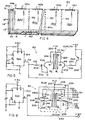
- Referring now to the drawings in greater detail, Figure 1 illustrates a
first embodiment 10 of an electrochromic assembly in accordance with the present invention in which a pair of electrochromic devices is optically aligned in a back-to-back, tandem arrangement. At least one of the devices is fully or partially transparent while the other device is operated or coloured by application of electrical energy to cause reduced light transmittance therethrough. As discussed more fully below, electrical circuitry may be included to alternately apply electrical energy to the two devices such that one is coloured or operated while the other is bleached for successive short periods of time thereby providing overall reduced light transmittance through the device without requiring extended coloration of either of the two devices in the assembly. -
Assembly 10 includes three aligned optical elements preferably formed from sheets of transparent material such as soda lime glass, acrylic plastic or the like.Elements elements front surfaces rear surfaces 12b, 14b and 16b andperipheral edges Central element 14 includes transparent electricallyconductive coatings opposite surfaces elements conductive coatings interior surfaces 12b and 16a which face thecentral element 14. Preferably, such conductive coatings may be formed from indium tin oxide, doped tin oxide, doped zinc oxide or the like as is conventionally known in the glass coatings industry. Although for reference purposes, surfaces indevice 10 are referred to as front and rear surfaces, it will be understood that the assembly may be useful with eitherelement -
Elements central element 14 fromsurfaces cavities cavities conductive coatings peripheral edges - Preferably, each of the
glass elements conductive coatings thin elements element 14 should be minimized as much as is practical. In this regard, the construction of Figure 1 is preferred. A suitable preferred choice forelement 14 would be thin (0.41 mm(0.016 inch)) soda lime glass coated on both of its opposing faces with an indium tin oxide (ITO) transparent conductive coating of sheet resistance of 15 ohms/square or better. - In order to apply electrical energy to the electrically
conductive coatings elements conductive coatings epoxy sealing materials conductive coatings seal materials elements - A suitable conductive paint or frit for
bus bars - The peripheral edge portions of the conductive bus bars 34, 36, 38 and 40 provide convenient attachment points for wire leads or
electrical connections - After application of the bus
bar perimeter coatings front surfaces 12b, 16a of front andrear elements Epoxy material space - If the assembly is to be used as a rearview mirror, a
reflective coating 42 preferably of metallic material such as aluminum, or a combination of silver and copper as is conventionally known, may be applied to the rear surface 16b ofelement 16 at a preferred thickness within the range of about 50 to 100 nanometres (500-1000 angstroms). Alternately, ifelement 16 will be the front element, the coating may be applied to thesurface 12a ofelement 12. Such coating may also be applied as a substitute forconductive coating 24 oninner surface 16a since the reflective coating is also electrically conductive. Other materials which may be used for the reflective layer include chromium, stainless steel, rhodium, platinum, palladium and/or combinations thereof. Such layer provides a highly specular surface which reflects approximately 40-95% of the incident light thereon through the other elements and the electrochromic medium inspaces element 16 in the event of a breakage or damage during collision in a vehicle, alayer 44 of tape or plastisol-type plastic adhesive typically about 0.1 millimetre thick is applied to the rear surface ofreflective coating 42. Such anti-scattering layer may be opaque, translucent or transparent since it is behind thereflective coating 42 and need not transmit or reflect any light. - After formation of the assembly as described above,
cavities - As mentioned above,
cavities - With these electrochromic or electrochemichromic materials, application of an electric field applied through
bus bars conductive coatings cavities layer 42 if such layer is included. In accordance with the present invention, however, an electrical switching circuit is used to successively and alternately colour and bleach electrochromic materials M1 and M2 such that neither quantity of electrochromic material is coloured for any extended period of time and usually for 60 seconds or less. Consequently, the effects of coloration segregation due to either voltage gradients or concentration gradients or the like are reduced to a negligible value or eliminated entirely. - When appropriate colouring or transmittance variation voltage is applied via bus bars 38, 40 and
conductive coatings cavity 28, the electrochromic material M2 colours under the applied voltage. Likewise, when appropriate colouring voltage is applied tobus bars conductive coatings cavity 26 colours. If appropriate colouring voltage is applied simultaneously to all of the bus bars and conductive coatings, electrochromic materials M1 and M2 in both cavities will both colour and the light transmission through both electrochromic devices will be at a minimum. If, however, a zero or bleach voltage is applied to bothcavities - In the preferred embodiment, a sequence of coloration of the two electrochromic devices is used such that, when viewed from either
element cavity 26 and electrochromic material M1 is initially operated and coloured for a time period sufficient to fully or partially reach its deepest coloration but short enough to avoid any significant coloration segregation. A typical period for this would be approximately 30 seconds although device design or construction can determine what time period is preferred. After 30 seconds or so, bus bars 34, 36 are shorted such that electrochromic material M1 begins to bleach while simultaneously electrical voltage is applied tobus bars assembly 10, when viewed from the side ofelement 12, will stay low. After approximately 30 seconds, bus bars 38, 40 are shorted and, preferably with polarity reversed, a coloration voltage is applied tobus bars assembly 10 can be operated indefinitely to provide reduced light transmission through the assembly for extended periods of time without leading to the normal disadvantages of voltage gradient induced and concentration induced coloration segregation or the like which normally affect long-term electrochromic device operation. Further, alternating reversal of polarity in applying the voltages to the spaced electrochromic media also helps to reduce coloration segregation by eliminating molecular migration toward any one charged conductive surface on a continuous basis. At any time during the sequence, the tandem, optically aligned electrochromic devices can be bleached simultaneously simply by shorting all of the bus bars 34, 36, 38 and 40 thereby returning to full light transmission simply by removing applied electrical energy from the electrochromic materials. This provides a proper fail-to-day mode, for instance, when the device is operated with areflective layer 42 as a vehicular rearview mirror. "Fail-to-day" means that, should all electrical power be lost in a vehicle using this mirror, the aligned devices would both bleach to their full reflectivity modes allowing safe, full, daytime visibility. - Further, should at any time it be desirable to simultaneously colour both of the two electrochromic devices, this can be done by simultaneously applying a full-or partial colouring voltage across bus bars 34, 36 and
bus bars - As shown in Figure 5, a suitable
electrical switching circuit 50 appropriate for use withelectrochromic assembly 10 is illustrated.Electrical circuit 50 provides application of suitable operating voltage to the electrochromic materials M1 and M2 inassembly 10 in alternating fashion for suitably short periods of time to avoid coloration segregation.Circuit 50 includes afirst voltage terminal 200 and asecond voltage terminal 202 across which are supplied a voltage of a level sufficient to colour electrochromic materials M1 and M2 to the desired level. In the illustrated embodiment, terminal 200 is connected with one volt DC andterminal 202 is connected with signal ground such thatcircuit 50 can apply one volt DC across materials M1 and M2.Terminal 200 is connected with wire leads 37, 39 extending toconductive coatings Circuit 50 further includes a first switch means 204 connected withlead 41 for alternatingly connectingconductive coating 20 betweenterminals transistor 206 whose emitter is connected withterminal 202 and whose collector is connected withlead 41 and, through abias resistor 208, withterminal 200. The base oftransistor 206 is connected through abias resistor 210 with anoutput line 212 of atiming device 214. -
Circuit 50 further includes a second switch means 216 connected withlead 35 for alternatingly connectingconductive coating 22 withterminals transistor 218 whose emitter is connected withterminal 202 and whose collector is connected withlead 35 and, through aresistor 220, withterminal 200. Switch means 216 further includes an invertingtransistor 222 whose emitter is connected with a source of voltage, such as five volts DC and whose collector is connected to aresistor 224 with the base oftransistor 218. The base oftransistor 222 is connected through aresistor 226 withoutput line 212. -
Timing device 214 is a conventional-type 555 integrated circuit, which is configured to alternate the signal online 212 between high and low states for periods of time between 30 and 40 seconds in each state. In a preferred embodiment, a time interval of 37 seconds is selected. Whenoutput 212 is in a low voltage state,transistor 206 is nonconducting and lead 41 is pulled to the level ofterminal 200 byresistor 208. Because leads 37, 39 are also at the level ofterminal 200, zero volt is applied across electrochromic material M2, which, therefore, bleaches to a transparent state. The low level online 212 causestransistor 222 to conduct which, in turn, causestransistor 218 to conduct. This pulls lead 35 to the level ofterminal 202. Accordingly, one volt DC is applied across material M1 which causes material M1 to colour. - When
output line 212 is at a positive voltage level, or high state,transistor 206 switches to a conducting state which pulls lead 41 to the level ofterminal 202, which applies one volt DC across material M2, causing material M2 to colour. The positive voltage andline 212switches transistors lead 35 to be pulled to the level ofterminal 200 throughresistor 220. This causes zero voltage to be applied across material M1, which bleaches. - Accordingly, as
output 212 oftimer 214 switches between high and low states, according to the timing interval set fortimer 214, materials M1 and M2 are alternatingly supplied with one volt DC and zero volt DC in opposite phase relationship. In a preferred embodiment, the interval oftimer 214 was selected to be 37 seconds. This interval is long enough for the alternate device in the assembly to fully bleach but not so long to allow the effect of segregation to be realized in the device being coloured. Ifcircuit 50 is applied to an assembly having electrochromic devices that takes longer to bleach than to colour, the time interval would be selected to be long enough to allow one device to bleach (or vice versa) without inducing segregation in the colouring device. - Alternately, an
electrical switching circuit 80 such as that shown in Figure 6 may be used to apply electrical voltage to the electrochromic materials M1 and M2 inassembly 10.Circuit 80 includes a first switch means 204′ in the form of arelay contact 228 which alternates connection oflead 41 between ajunction 230 and terminal 202 and a second switch means 216' in the form of arelay contact 232 which alternates connection oflead 35 betweenjunction 230 andterminal 202.Relay contacts common relay solenoid 234.Relay solenoid 234 is connected in series between a source of 12 volts DC andoutput line 212 such thatrelay contact timing device 214.Junction 230 is connected withterminal 200 through aresistor 236. -
Circuit 80 further includes a two-pole, triple position switch means 238 which incorporates a first contact 240a and asecond contact 240b. This can be a manually operated triple position switch. Whenswitch 238 is selected so that contact 240a is connected directly to first switch means 204′ and so thatcontact 240b is connected to second switch means 216′, one device colours while the other device bleaches with the selection being dependent on the respective connection made byrelay contacts contacts 240a, 240b are positioned such that leads 35, 41 are connected directly withterminal 200,terminals switch 238 is selected so thatcontacts 240a, 240b are positioned so that leads 41, 35 are connected directly with leads 141, 135, the voltage applied to the circuit throughterminal 200 is concurrently applied across both electrochromic devices in the tandem assembly such that electrochromic materials M1 and M2 both colour simultaneously and such that the net transmission through the tandem assembly is at a minimum. -
Circuit 80 further includes a fail-to-day switch means 500 such that, when power is lost, leads 35, 41 are connected to terminal 200 so thatterminals relay contacts terminal 200. -
Circuit 80 operates substantially the same ascircuit 50 except thatrelay solenoid 234 andcontacts transistors resistor 236 is to reduce the rate of bleaching of materials M1 and M2, which occurs wheneverrelay contacts respective leads junction 230. The resistance ofresistor 236 limits the current developed as the corresponding electrochromic material is bleached. The reason that the rate of bleach is slowed is that certain electrochromic material partially bleaches in a shorter period of time than it deeply colours. Thus, the value ofresistor 236 is selected to decrease the rate of bleaching to more closely match the rate of coloration. In the illustrated embodiment,resistor 236 is selected to be 67 ohms. - Other methods could be employed in order to compensate for the difference between the rate of coloration and the rate of bleaching. As shown in Figure 8, switching
circuit 250 includes a pair of power sources PPS1 and PPS2 which can be configured to begin coloration prior to bleaching of the opposite element. Each power source PPS1 and PPS2 is capable of supplying a voltage to itsrespective terminal terminals - A
digital switching circuit 300 is shown in Figure 10 suitable to use to alternately power the two electrochromic devices in the tandem assembly, with overlap in their colour times, thus minimizing the fluctuation in dimmed state reflectivity caused by the one cell not colouring (in percentage terms) as deeply as the other cell partially bleaches. To accomplish the desired result, the devices in the tandem assembly should be driven 180° out of phase and the duty cycle (duration of colour portion of the powering cycle compared to the duration of the bleach portion of the same powering cycle) should be greater than 50/50. Aclock circuit 302 is the source clock and is set for a frequency that is 16 times greater than the desired frequency of the electrochromic device drive. Anintegrated circuit 304 is a 4-bit binary counter that continually counts up in a unit binary value on each rising edge of the clock signal generated byclock circuit 302 and which provides inputs onlines 310 for both of comparator integratedcircuits lines 310 ranges from 0-15 and then restarts at 0 again. Comparator integratedcircuits Switch circuit 300 uses the A>B output pins 312 and 314 of the comparators to generate signals that serve as inputs to Darlington transistors Q1, Q2 connected respectively betweenterminals comparators integrated circuit 304. With the B value set to 6, an A value from 0-6 will produce a low state (zero volt) on the A>B output pin, and values 7-15 produce a high state (Vcc) on the A>B output pin. When A>B output respective terminal terminals output respective terminal terminals resistor comparator 308 usinginverter 324. - The time variation of the voltage signals across leads 35, 41 and ground are shown in Figure 11. In general, it is desirable when using electrochromic devices, such as are described in EP-A-0430684, to use a colour/bleach duty cycle of 3:2. Also, it is preferable that the duration of the coloration portion of the duty cycle be appropriately short but it is also important that the bleach duration by sufficiently long to allow a given device to fully bleach during its bleach portion of the duty cycle. It has been discovered that a 30 second colour:20 second bleach (or thereabouts) duty cycle works well. Application of two such signals, 180° mutually out of phase as shown in Figure 11, insures that adequate overlaps exist to accommodate the differences in coloration and bleaching rates in the respective devices in the tandem assembly. Two examples of overlap are indicated by the dashed region E, F in Figure 11. A suitable choice for the time duration of the overlap regions is half the difference between the coloration portion and the bleach portion of the duty cycle. For a 30 second colour:20 second bleach duty cycle, this is five seconds which, for the particular example shown in overlap region E in Figure 11, means that electrochromic material M2 in the one device begins to colour five seconds before the already coloured electrochromic material M1 begins to bleach in the other device. Such overlap insures that the one device incorporating electrochromic material M2 is deeply coloured in advance of the other device incorporating electrochromic material M1 commencing bleaching. Thus, there is no transient significant increase in net transmission through the tandem assembly due to the switchover from colouring one device to colouring the other.
- Other modifications to the circuit are possible. Instead of applying a fixed voltage across
terminals terminals - Use of the tandem, optically aligned construction as shown in
assembly 10 in conjunction with appropriate drive circuitry such as that shown at 50 and 80 in Figs. 5 and 6 is also particularly useful in large area electrochromic devices. When voltage is applied to such devices via bus bars which circumscribe the perimetal edge regions, coloration in large area devices, such as automotive sunroofs and the like, typically commences at the edges and lags somewhat in the centre. This leads to an iris-like effect such that dimming and coloration occurs as a wave from the edges toward the centre. Further, because of leakage currents, and particularly in electrochemichromic devices, the central region may not dim as dark as edge regions which are closer to the bus bars and suffer from less voltage reduction than is experienced in more remote central regions. Upon application of zero or reverse bleaching voltage, the opposite is true. Thus, when electrochromic devices are shorted, the edge regions bleach first and the central region remains coloured until it, too, finally bleaches. However, by using the tandem construction as shown inassembly 10, and by colouring electrochromic material M1 while simultaneously bleaching material M2, the iris effect incavity 26 during coloration can be matched to the inverse iris effect incavity 28 during its bleaching phase such that the net coloration, as seen when viewing the tandem construction, appears to be uniform. This sequence is initiated by first applying voltage to colour or dim either of electrochemichromic materials M1 or M2 and thereafter, applying appropriate balancing of the coloration and bleaching of theindividual cavities - As is also shown in Figure 1, operation of
assembly 10 may be enhanced by inclusion of an anti-reflection means 46 on one or both ofsurfaces 12a and/or 16b, the outermost surfaces of the assembly. The use of such an anti-reflective coating or coatings provides significant glare and double image reducing advantages for all types of electrochromic assemblies including those using flat, curved or convex or multi-radius glass, for both interior and exterior vehicle applications and other uses. Layer orcoating 46 is an optically transparent, thin film such as magnesium fluoride (MgF2) having a refractive index of about 1.38 at 600 nm and deposited at a thickness of about 0.1075 micrometres (1075 angstroms) onto thesurface 12a or 16b of one of the elements. When light is incident in air on the surface of such a coated element at 22.5°C, which is typical for standard measurement of reflection from vehicular rearview mirrors under SAEJ964a, the reflectivity of the coated surface is 1.4% of the incident light as viewed by the human eye. Reflectivity for an uncoated surface under the same conditions is approximately 4.2% of the incident light. Multiple layer thin films and other coating constructions may also be used. - An
alternate form 110 of the electrochromic assembly is shown in Figure 2 where like numerals indicate like parts to those inassembly 10.Assembly 110 includes acomposite centre element 14′ including a pair of glass panels orsheets polyvinyl butyral interlayer 116 as is conventionally known in the automotive glass industry. A suitable material isSAFLEX SR# 11 from Monsanto Company of St. Louis, Missouri.Polymeric layer 116 is applied between surfaces 112b and 114a ofelements elements glass elements -
Assembly 110 may also include areflective layer 42, a shatter preventing plastisol ortape layer 44, and/or ananti-reflective coating 46 on one or both exterior surfaces depending on the location of the reflective and anti-shatter layers. Laminate constructions, as described in EP-A-0437914, can be used for either or both ofglass elements central element 14′ to achieve UV protection, safety and/or tinted effects. As withassembly 10,cavities conductive coatings other seals conductive coatings assembly 10 to reduce overall coloration segregation effects. - As an alternative to
polymer layer 116, an optically transparent adhesive such as NORLAND 65, available from Norland Products, Inc., New Brunswick, New Jersey, may be used to adhereelement 112 toelement 114. Such an adhesive is water clear, highly transparent to visible light, includes a moderate modulus of elasticity when cured such that it is not overly brittle, does not fracture upon impact, and includes an index of refraction of 1.54 matched closely to that of soda lime glass which has a refractive index of 1.52. It also has a relatively low viscosity such that it easily pours and spreads between the two glass panels to allow lamination and bonding once cured. Use of such an optical adhesive or theintermediate polymer layer 116 for laminatingelements - Yet another
form 130 of the electrochromic assembly is shown in Figure 3 where like numerals indicate like parts to those inassemblies Assembly 130 differs from the other assemblies by the inclusion of a slight offset ofcentre element 14˝ from the positions of the front andrear elements assembly 130 includes refractive index matched thin film means 132, 134, 136 and 138 on the inner surfaces of the elements to reduce interfacial reflections and to enhance overall light transmission. - As shown in Figure 3,
assembly 130 includesglass elements central element 14˝ in parallel relationship byseals conductive coatings assembly 10, intermediate thin film means 132, 134, 136, 138 are provided intermediate insidesurfaces conductive coatings element 12 prior to coating ofconductive layer 22 thereover. Likewise, thin film means 134 is applied tosurface 14a, thin film means 136 is applied tosurface 14b and thin film means 138 is applied tosurface 16a prior to application ofcoatings glass elements cavities - In addition to
thin films central element 14˝ is offset slightly with respect toelements elements conductive ribbon connectors elements elements ribbon connectors conductive coatings assemblies reflective coating 42 and/or plastisol ortape layer 44, as well as ananti-reflection coating 46, are included on various surfaces of the assembly as described above. - Figure 4 illustrates another
embodiment 150 of an electrochromic assembly in accordance with the present invention similar toassembly 110 of Figure 2 and includingouter elements central element 14˝′.Assembly 150 was built and tested as set forth below.Central element 14˝′ is offset with respect to the positions ofelements assembly 130 in Figure 3.Elements Central element 14˝′ is formed by laminating two 1.60 mm (0.063 inch) 15 ohms per square ITO coated glass panels, back-to-back in tandem, using NORLAND 65 optical adhesive. Epoxy seals such as those as 30, 32 described above are used to contain the electrochemichromic material.Elements Spaces M 5,10-dihydro-5,10-dimethylphenazine, and 5% weight per volume Uvinul 400 UV stabilizer from BASF Wyandotte, Wyandotte, Michigan, dissolved in a solvent consisting of a 50%:50% by volume mixture of 3-hydroxypropionitrile and 3,3′-oxydipropionitrile. The dimensions of each glass panel are 150mm (six inches) by 50mm (two inches). - Prior to assembly,
conductive coating 22 oninside surface 12a ofelement 12 was segmented into six 25mm (one inch) by 50mm (two inch) pixels or areas by sandblasting insulating ordeletion lines 152 roughly 0.5 mm in width across the entire element to divide the coating into six ITO coated regions 154a, 156a, 158a, 160a, 161a, 162a, each region being insulated from the other by the sandblasted deletion line. Likewise, ITOconductive coating 24 onelement 16 was similarly partitioned with deletion lines into areas 154b, 156b, 158b, 160b, 161b and 162b such that the tandem assembly included the deletion or insulating lines and separate coated areas on bothelements element 12. A commonmetallic ribbon connector 142 was attached to joinITO coatings central element 14˝′, a portion ofribbon connector 142 being shown in Figure 4. Twelve individual,shorter ribbon connectors 140a, b, c, d, e and f and 144a, b, c, d, e and f were attached to the extending edges ofelements connector 142 toconductive coatings central element 14˝′, and any one of the twelveribbon connectors elements -
Assembly 150 was used by applying a one volt potential to vary the transmission and colour of pixel or area 156a, i.e., the second area from the left in Figure 4. Such one volt potential was applied for a period of one hour. When a bleach voltage (zero volt) was first applied after such prolonged coloration, severe coloration segregation was noted principally due to concentration gradient segregation. Hence, areas 154a and 158a on either side of area 156a were partially coloured after such coloration such that it took approximately 30 minutes for recombination reactions within the electrochemichromic fluid to reduce the bands of coloration seen after such operation. When the following sequence was used in operation ofassembly 150, no equivalent coloration segregation effect was noted even after prolonged coloration for 24 hours:
- As another example, an interior rearview mirror assembly was fabricated using the electrochromic/ electrochemichromic formulation, cell construction and tandem assembly described above, especially as shown in Figure 3. The sample produced was roughly 230mm (nine inches) long by 50mm (two inches) wide and was in the shape of a conventional, elongated, rectangular interior rearview mirror. The rear surface 16b of the rearmost electrochromic device was coated with a
reflective coating 42 as described above such that light entering through thefront surface 12a of the forwardmost electrochromic device passed through both devices, was reflected off thereflective surface 42, and passed a second time through both devices before exiting to the viewer's eye. As measured using SAE Standard J964a for automotive mirror reflectivity, the light reflectance of thetandem assembly 130 as constructed above was 70.6% with both devices in their fully bleached, noncoloured state. When the assembly was operated using a circuit such as that shown in Figure 6, withswitch 238 set so that one device coloured while the other device bleached through the operation ofrelay contacts surfaces 12b and 14a was solely coloured at one volt, and 7.8% which was the lowest reflectance achieved if the rearmost device betweensurfaces - Figure 7 is a graph of the operation of this rearview mirror where the vertical axis is reflectance and the horizontal axis is time, the graph being recorded at a chart speed of one centimetre per minute. The first reflectance transient, labelled F1, was due solely to coloration of the forwardmost device between
elements elements elements - A rearview mirror configured tandemly and powered such that the one device coloured when the other device bleached using a circuit as described above in Figure 6 was left in its coloured, dimmed state for over 60 hours without any perceptible sign of the affects of coloration segregation. At any time during prolonged coloration, the fully bleached state was achievable simply by switching
switch 238 so that leads 35, 41, 37, 39 were directly interconnected. The substantially total elimination of such segregation in embodiments according to the present invention, even after an indefinite period of coloration, is a significant improvement and allows use of manually activated, remote control rearview mirrors where, under such manual control, the mirrors can be partially or fully dimmed at the direction and selection of the vehicle driver for periods of up to several hours without coloration segregation occurring. - Such concepts are also equally useful in window assemblies. For example, a window device of roughly 220mm (8.75 inches) by 70mm (2.75 inches) was constructed using the concepts described above. In the fully bleached mode, light transmission through the tandem assembly was about 76.5%. When operated by the circuit of Figure 6, the transmission dimmed to a low value between 10.6% and 13.9%. Even when dimmed for a period exceeding 60 hours, no coloration segregation was seen upon first bleaching after such prolonged operation. Further, when a potential of one volt was applied to concurrently colour both devices, the transmission of the tandem assembly achieved a minimum of 1.8%.
- An electrochromic device of the single-compartment, solution-phase, self-erasing type could be tandemly combined with a thin film type electrochromic device such as are described in the article "Automotive Applications of Chromogenic Materials" by Niall R. Lynam and Anoop Agrawal as published in the book Large Area Chromogenics: Materials and Devices for Transmittance Control, edited by Carl M. Lampert and Claes G. Granqvist, SPIE Optical Engineering Press, Bellingham, Washington, 1990. Indeed, in the specific case of all solid-state devices, one of the tandem electrochromic devices could be a stack of thin films deposited onto the outer surface of a twin substrate laminate cell as described previously. Indeed, in the broadest sense, only one substrate may be needed if all solid-state electrochromic (EC) stacks are deposited on opposing faces of the same, single glass substrate.
- In several electrochromic assembly designs and particularly in the case of electrochemichromic devices, speed of response, and in particular speed of bleaching, is related to cell thickness. Thus, for fast speed of response, thinner cell thicknesses (30-125 micrometres) are desirable. However, this beneficial increase in speed of response can be accompanied by a decrease in the depth of coloration. As a consequence, when a rearview mirror is constructed using a single electrochromic device, the reflectivity achieved is often not less than 10%. While this level of glare reduction is satisfactory in many driving conditions, it fails to provide the deep level of coloration required for reflectivity values in the 4-8% range commonly specified by automakers for extreme anti-glare protection.
- By using the tandem construction of the invention, thinly spaced EC devices with desirably fast colour and bleach rates can achieve the moderate anti-glare protection levels desired in most driving conditions by colouring one device while bleaching the other. The deepest levels of coloration can be achieved by concurrent coloration of both tandem devices. While this is useful in remotely activated vehicular mirror systems having a low reflectance override state, the desired attributes of this aspect of the invention can be realized both in automatic and semi-automatic controls, whereby glare detectors and ambient detectors are used to select whether the electrochromic devices are sequentially or concurrently actuated and, for either mode, the depth of coloration desired.
- In office partitions, sunroofs and security/privacy windows, building windows and similar applications, the concurrent operation feature of the examples of the invention is capable of providing extra privacy or security, or extra light attenuation performance, through its rapid attainment of deep coloration. During those periods when great depth of coloration, and hence low light transmission, is achieved through concurrent operation, the prolonged application of an electrical field to the EC device may cause segregation. However, such segregation may be preferable in view of the extra privacy, performance or security. For electrochromic devices where means such as the aforementioned thickeners or low leakage-current solvents have been incorporated to minimize the effect of segregation, longer periods of concurrent operation can be attainable.
- Also, more than two electrochromic devices as described herein could be assembled in an optically aligned back-to-back arrangement. For example, three devices could be assembled together allowing choice of colouring any two while the third bleaches, colouring only one while the other two bleach or colouring all concurrently. Likewise, if more than three devices are optically aligned in back-to-back assembly, a wide range of choices for cyclical powering of some of these while the remainder bleach, could be made. Further, concurrent colouring of all devices, or a subset thereof, would allow attainment of minima in overall light transmission through the complete assembly.
- Therefore, it will be understood that the embodiments shown in the drawings and described herein are merely for illustrative purposes, and are not intended to limit the scope of the invention.
- In a preferred embodiment, the assembly comprises first and second optically aligned electrochromic devices defined by a sheet of transparent material, first and second layers of electrochromic material adjacent opposing surfaces of said sheet, the transmittance of each of said layers being variable when an electrical field is applied thereacross, and electrical means for applying an electrical field across each of said layers of electrochromic material; and switch means for first applying electrical power to one of said first and second devices for a first short period of time to cause coloration of said one device while bleaching the other of said devices to a colourless, substantially transparent state and secondly applying electrical power to said other device for a second short period of time to cause coloration of said other device while bleaching said one device to a substantially colourless, transparent state, and thereafter alternately applying electrical power and bleaching said devices cyclically in the same manner; whereby coloration segregation in both of said first and second devices is reduced when said assembly is operated over prolonged periods of time. The assembly may include a reflective coating adapted to reflect light incident thereon through said first element and said electrochromic material.
- In another embodiment, the assembly preferably comprises first, second and third optically transparent elements aligned generally in tandem with one another, each element having a peripheral edge and front and rear surfaces, said third and second elements being spaced respectively from said front and rear surfaces of said first element; at least one of a liquid, thickened liquid, gel and semi-solid electrochromic material confined in said spaces adjacent both surfaces of said first element, said electrochromic material having a light transmittance which varies when an electric field is applied thereacross;
seal means extending around the periphery of said assembly for spacing said elements apart and confining said electrochromic material within said spaces; electrical means for selectively applying electrical power for short periods of time across said electrochromic material in one of said spaces to reduce the light transmittance therethrough and for selectively bleaching at other times said electrochromic material in said one of said spaces, and for selectively applying electrical power for short periods of time across said electrochromic material in said other space and for selectively bleaching at other times said electrochromic material in said other space, whereby coloration segregation in said electrochromic material in both said spaces is reduced when said assembly is operated over prolonged periods of time and the depth of coloration of said assembly may be made greater than that from one of said spaces. - In this embodiment, the first element preferably includes a pair of transparent sheets adhered to one another with an optically transparent material, and these are preferably laminated to one another with a polymer layer. In the same preferred embodiment it is preferred that the electrical means includes means for causing the electrochromic material in said other space to bleach simultaneously with the application of electrical power to the electrochromic material in said one space, and vice versa during continued, cyclical operation of said assembly or that the electrical means includes means for applying electrical power to the electrochromic material in said other space immediately following application of electrical power to the electrical power in said one space, and vice versa during continued, cyclical operation of said assembly.
- In a further preferred embodiment, the assembly comprises first and second tandemly mounted electrochromic elements, each of said elements having a layer of electrochromic material, the transmittance of which varies when an electrical field is applied thereacross and a pair of electrically conductive busses adapted to applying an electrical field across said layer; a power source including first and second power terminals and means for applying electrical power thereacross, said power source being adapted to changing each of said elements from a substantially transparent condition to a coloured condition; means for connecting one of said power terminals to one of said busses of each of said elements; first switch means for alternatingly connecting the other one of said busses of one of said elements to said first and second power terminals; second switch means for alternatingly connecting the other one of said busses of the other one of said elements to said first and second power terminals; and control means for causing said first and second switch means to switch between said first and second power terminals. This embodiment may further include third switch means for selectively disabling said first and second switch means and for shorting said busses in each of said electrochromicelements, and the voltage across said power terminals is preferably variable.
- In an alternative preferred embodiment, the assembly comprises first and second optically aligned electrochromic devices defined by a sheet of transparent material, first and second layers of electrochromic material adjacent opposing surfaces of said sheet, the transmittance of each of said layers being variable when an electrical field is applied thereacross, electrical means for applying an electrical field across each of said layers of electrochromic material; and switch means for selectively applying electrical power to said first and second devices.
Claims (31)
- An electrochromic assembly (10,110,130,150) comprising, first and second optically aligned electrochromic devices which comprise first and second layers (M1,M2) of electrochromic material located adjacent opposing surfaces of transparent sheet material, each layer being adapted to vary in transmittance when an electrical field is applied thereacross, electrical means (18, 20, 22, 24, 34, 35, 36, 37, 38, 39, 40, 41) for applying an electrical field across each layer, and switch means (50,80,250,300) for selectively applying electricity to the first and second devices.
- An assembly as claimed in claim 1 in which the switch means includes means (204,216,204′,216′) adapted to apply electricity cyclically and alternatingly to the first and second devices in order to cause coloration of one said device while bleaching the other said device and vice versa.
- An assembly as claimed in claim 1 or claim 2 which is adapted to apply a variable quantity of electricity to the first and second devices.
- An assembly as claimed in claim 3 in which the variable quantity is voltage.
- An assembly as claimed in any one of the preceding claims in which the switch means includes means (238) for applying electricity concurrently to the first and second devices such that the depth of coloration of the assembly is greater than that provided by each device alone.
- An assembly as claimed in any one of the preceding claims in which the switch means includes means (214,302) for periodically reversing the polarity of the electricity applied to the devices.
- An assembly as claimed in any one of the preceding claims in which a said device includes a first space defined by first and second spaced optically transparent elements (14,16) each having a peripheral edge and front and rear facing surfaces (14a,14b,16a,16b).
- An assembly as claimed in claim 7 which includes a second space defined by a third optically transparent element (12) being spaced from the first element (14), the third element having a peripheral edge and front and rear facing surfaces (12a,12b)
- An assembly as claimed in claim 8 in which the electrical means includes first and second power terminals (200,202) and means for connecting the first terminal to the first element (14), and the switch means are adapted to switch between first and second states, the first state having the first terminal connected to the second element (16) and the second terminal connected to the third element (12), the second state having the first terminal connected to the third element and the second terminal connected to the second element.
- An assembly as claimed in any one of claims 7 to 9 in which the electrochromic material in a said device includes at least one of a liquid, thickened liquid, gel and semi-solid electrochromic material confined in a said space, seal means (30,32) extends around the entire periphery of the assembly and between the first and another said element (12,14,16) adjacent their peripheral edges for spacing the elements apart and confining the electrochromic material in the said space, the electrical means includes an electrically conductive coating (18,20,22,24) on the facing surfaces (14b,16a,14a,12b,114b,112a) of the elements, the electrochromic material (M2) being in contact with the conductive coatings, and connector means (38,40,142,144) being adapted to connect an electrical lead (39,41) to each conductive coating.
- An assembly as claimed in claim 10 in which the first (14˝) and second (16) elements are offset from one another such that portions of the conductive coatings (18,20,22,24) are exposed adjacent the peripheral edges of the elements, the connector means including a clamp type metallic ribbon connector (142,144) secured to each offset element edge, each ribbon connector being adapted to contact at least one conductive coating.
- An assembly as claimed in claim 10 or claim 11 in which the electrically conductive coatings (18,20,22,24) of both devices include a plurality of areas (154,155,156,157,158,159,160,161,162) spaced from one another by uncoated deletion lines (152), the areas in the respective devices being optically aligned and in registry with one another, whereby the transmittance of at least one pair of areas may be varied separately from the remainder of the areas for prolonged periods of time with reduced color segregation.
- An assembly as claimed in any one of claims 7 to 12 in which a said element (16) includes a surface (16b) having a reflective coating (42) adapted to reflect incident light through the assembly.
- An assembly as claimed in claim 13 in which the reflective coating (42) reflects incident light through another said element (12,14) and the electrochromic material (M1,M2).
- An assembly as claimed in any one of claims 7 to 14 in which includes an anti-reflective coating (46) on the outermost surface (12a) of a said element (12) to provide lower total relfectivity and reduced double imaging.
- An assembly as claimed in any one of claims 7 to 15 in which a surface of a said element which faces another said element includes a thin film, the film having an index of refraction below that of the said element to which it is applied, the combined indices of refraction of the said element and the thin film being generally matched to that of the electrochromic material.
- An assembly as claimed in any one of claims 7 to 16 in which the devices are secured by an optically transparent material (116).
- An assembly as claimed in claimed 17 in which the transparent securing material is an adhesive having an index of refraction substantially matched to the index of refraction of the transparent elements.
- An assembly as claimed in claim 17 or claim 18 in which a said transparent element of the first device (114) is laminated to a said transparent element of the second device with a polymer layer (116).
- An assembly as claimed in any one of the preceding claims which includes means (500) adapted to operate upon electrical power failure for shorting out the electrical field across each device.
- An assembly as claimed in any one of the preceding claims in which the electrical means are adapted to apply an electrical field to selected areas (154,155,156,157,158,159,160,161,162) of the assembly, the areas being optically aligned and in registry with one another, whereby the transmittance of at least one pair of areas may be varied separately from the remainder of the areas for prolonged periods of time with reduced color segregation.
- An assembly as claimed in any one of the preceding claims in which the switch means is adapted first to apply electricity for a first short period of time to cause coloration of the first device while bleaching the second device to a substantially colorless transparent state and second to apply electricity to the second device for a second short period of time to cause coloration of the other second device while bleaching the first device to a substantially colorless transparent state and thereafter to apply electricity and bleach the devices alternately and cyclically in the same manner.
- An assembly as claimed in claim 22 in which the switch means includes means for causing one device to begin coloration during the time period in which the other device is at least partially colored during the alternating cyclical operation, whereby adjustment is made for matching bleaching rates as compared to coloration rates in the devices.
- An assembly as claimed in claim 22 in which the switch means includes means for causing one device to color simultaneously with the bleaching of the other device for the same period of time, and vice versa during continued cyclical operation of the assembly.
- An assembly as claimed in claim 22 in which the second short period of time immediately follows the first short period of time.
- An assembly as claimed in claim 22 in which the switch means includes compensation means (208,220,320,322) adapted to adjust one of the bleaching and coloration rates to match the other.
- An assembly as claimed in any one claims 1 to 21 in which the switch means is adapted to apply electricity across the electrochromic material in one device during the time period in which electricity is applied across the electrochromic material in the other device, and vice versa during continued alternating operation, whereby adjustment is made for bleaching rates as compared to coloration rates of the electrochromic materials in the spaces.
- An assembly as claimed in any one of claims 1 to 21 in which a pair of electrically conductive busses (34,36,38,40) are adapted to apply an electrical field across each device; the electrical means include a power source including first and second power terminals (200,202) and means for applying electricity thereacross; means (37,39)are adapted to connect a said power terminal to one said bus of each said device; the switch means comprising first switch means (204,204′,308) for alternatingly connecting the other said bus of one said device to the first and second power terminals and second switch means (216,216′,306) for alternatingly connecting the other said bus of the other said device to the first and second power terminals; and control means (214,304) are adapted to cause the first and second switch means to switch between the first and second terminals.
- An assembly as claimed in claim 28 in which the control means is adapted to cause the first and second switch means to alternatingly switch repetitively between the first and second power terminals whereby the power source may be applied across one device while a short circuit is applied across the other device.
- An assembly as claimed in claim 28 or claim 29 in which the first switch means is adapted to begin to apply a voltage across one device concurrently with the second switch means beginning to apply a short circuit across the other device, and vice versa.
- An assembly as claimed in any one claim of claim 9 or claims 28 to 30 in which the electrical means includes an impedance device (208,220,320,322) in electrical series connection between a said switch means and a said power terminal (200).
Applications Claiming Priority (2)
| Application Number | Priority Date | Filing Date | Title |
|---|---|---|---|
| US07/565,660 US5076673A (en) | 1990-08-10 | 1990-08-10 | Prolonged coloration electrochromic assembly |
| US565660 | 2000-05-05 |
Publications (2)
| Publication Number | Publication Date |
|---|---|
| EP0470867A2 true EP0470867A2 (en) | 1992-02-12 |
| EP0470867A3 EP0470867A3 (en) | 1992-09-23 |
Family
ID=24259596
Family Applications (1)
| Application Number | Title | Priority Date | Filing Date |
|---|---|---|---|
| EP19910307388 Withdrawn EP0470867A3 (en) | 1990-08-10 | 1991-08-12 | Electrochromic assembly |
Country Status (3)
| Country | Link |
|---|---|
| US (1) | US5076673A (en) |
| EP (1) | EP0470867A3 (en) |
| IE (1) | IE911980A1 (en) |
Cited By (14)
| Publication number | Priority date | Publication date | Assignee | Title |
|---|---|---|---|---|
| EP0652462A1 (en) * | 1993-11-05 | 1995-05-10 | Kabushiki Kaisha Tokai Rika Denki Seisakusho | Anti-glare electrochromic mirror |
| EP0676059A1 (en) * | 1992-12-24 | 1995-10-11 | Sun Active Glass Electrochromics, Inc. | Electrochromic devices |
| EP0818600A2 (en) * | 1992-05-21 | 1998-01-14 | Saint-Gobain Vitrage | Electrochromic glazing |
| FR2751097A1 (en) * | 1996-07-10 | 1998-01-16 | Saint Gobain Vitrage | ELEMENTS WITH VARIABLE OPTICAL / ENERGY PROPERTIES |
| WO2004015674A1 (en) * | 2002-07-26 | 2004-02-19 | Koninklijke Philips Electronics N.V. | Electrochromic color display having different electrochromic materials |
| WO2010033485A3 (en) * | 2008-09-17 | 2010-07-01 | Soladigm, Inc. | Electrical contact technique for electrochromic window |
| FR2960073A1 (en) * | 2010-10-07 | 2011-11-18 | Commissariat Energie Atomique | All-solid electrochromic display device i.e. polychromatic display device, has green color electrode constituting receiving electrode, where specific ion rate of receiving electrode is defined by specific equation comprising parameters |
| US9341912B2 (en) | 2012-03-13 | 2016-05-17 | View, Inc. | Multi-zone EC windows |
| US9341909B2 (en) | 2008-06-25 | 2016-05-17 | View, Inc. | Multi-pane dynamic window and method for making same |
| US9581875B2 (en) | 2005-02-23 | 2017-02-28 | Sage Electrochromics, Inc. | Electrochromic devices and methods |
| EP2047325B1 (en) * | 2006-07-21 | 2017-04-26 | Sage Electrochromics, Inc. | Glass type electrochemical/ electrically controllable device with variable optical and/or energetic characteristic |
| US10429712B2 (en) | 2012-04-20 | 2019-10-01 | View, Inc. | Angled bus bar |
| US10481458B2 (en) | 2013-06-18 | 2019-11-19 | View, Inc. | Electrochromic devices on non-rectangular shapes |
| US11635666B2 (en) | 2012-03-13 | 2023-04-25 | View, Inc | Methods of controlling multi-zone tintable windows |
Families Citing this family (232)
| Publication number | Priority date | Publication date | Assignee | Title |
|---|---|---|---|---|
| FR2666804B1 (en) * | 1990-09-14 | 1993-05-28 | Saint Gobain Vitrage Int | ELECTROCHROME GLAZING. |
| US5220317A (en) * | 1990-12-11 | 1993-06-15 | Donnelly Corporation | Electrochromic device capable of prolonged coloration |
| US5724177A (en) * | 1991-09-04 | 1998-03-03 | Sun Active Glass Electrochromics, Inc. | Electrochromic devices and methods |
| US5910854A (en) | 1993-02-26 | 1999-06-08 | Donnelly Corporation | Electrochromic polymeric solid films, manufacturing electrochromic devices using such solid films, and processes for making such solid films and devices |
| US5657150A (en) * | 1993-09-10 | 1997-08-12 | Eyeonics Corporation | Electrochromic edge isolation-interconnect system, process, and device for its manufacture |
| US5668663A (en) | 1994-05-05 | 1997-09-16 | Donnelly Corporation | Electrochromic mirrors and devices |
| US6891563B2 (en) | 1996-05-22 | 2005-05-10 | Donnelly Corporation | Vehicular vision system |
| FR2738813B1 (en) * | 1995-09-15 | 1997-10-17 | Saint Gobain Vitrage | SUBSTRATE WITH PHOTO-CATALYTIC COATING |
| US5856211A (en) * | 1996-04-10 | 1999-01-05 | Donnelly Corporation | Method for filling the cavities of cells with a chromogenic fluid |
| US5824374A (en) * | 1996-07-22 | 1998-10-20 | Optical Coating Laboratory, Inc. | In-situ laser patterning of thin film layers during sequential depositing |
| US6039390A (en) * | 1996-08-20 | 2000-03-21 | Donnelly Corporation | Chromogenic window assembly construction and other chromogenic devices |
| US6111684A (en) * | 1997-04-02 | 2000-08-29 | Gentex Corporation | Electrochromic rearview mirror incorporating a third surface metal reflector and a display/signal light |
| US5818625A (en) * | 1997-04-02 | 1998-10-06 | Gentex Corporation | Electrochromic rearview mirror incorporating a third surface metal reflector |
| US6089721A (en) | 1997-04-02 | 2000-07-18 | Donnelly Corporation | Digital electrochromic mirror system |
| US6166848A (en) * | 1997-04-02 | 2000-12-26 | Gentex Corporation | Electrochromic rearview mirror incorporating a third surface metal reflector and a display/signal light |
| US6356376B1 (en) * | 1997-04-02 | 2002-03-12 | Gentex Corporation | Electrochromic rearview mirror incorporating a third surface metal reflector and a display/signal light |
| US6700692B2 (en) | 1997-04-02 | 2004-03-02 | Gentex Corporation | Electrochromic rearview mirror assembly incorporating a display/signal light |
| US6056410A (en) | 1997-04-02 | 2000-05-02 | Donnelly Corporation | Digital electrochromic mirror system |
| US6124886A (en) | 1997-08-25 | 2000-09-26 | Donnelly Corporation | Modular rearview mirror assembly |
| US6326613B1 (en) | 1998-01-07 | 2001-12-04 | Donnelly Corporation | Vehicle interior mirror assembly adapted for containing a rain sensor |
| US8294975B2 (en) | 1997-08-25 | 2012-10-23 | Donnelly Corporation | Automotive rearview mirror assembly |
| US6172613B1 (en) | 1998-02-18 | 2001-01-09 | Donnelly Corporation | Rearview mirror assembly incorporating vehicle information display |
| US8288711B2 (en) | 1998-01-07 | 2012-10-16 | Donnelly Corporation | Interior rearview mirror system with forwardly-viewing camera and a control |
| US6445287B1 (en) | 2000-02-28 | 2002-09-03 | Donnelly Corporation | Tire inflation assistance monitoring system |
| US6477464B2 (en) | 2000-03-09 | 2002-11-05 | Donnelly Corporation | Complete mirror-based global-positioning system (GPS) navigation solution |
| US6693517B2 (en) | 2000-04-21 | 2004-02-17 | Donnelly Corporation | Vehicle mirror assembly communicating wirelessly with vehicle accessories and occupants |
| US6329925B1 (en) | 1999-11-24 | 2001-12-11 | Donnelly Corporation | Rearview mirror assembly with added feature modular display |
| US6553308B1 (en) | 1999-04-29 | 2003-04-22 | Donnelly Corporation | Vehicle-based navigation system with smart map filtering, portable unit home-base registration and multiple navigation system preferential use |
| US6084700A (en) * | 1998-04-29 | 2000-07-04 | Gentex Corporation | Reflectance control of an electrochromic element using a variable duty cycle drive |
| US6317248B1 (en) | 1998-07-02 | 2001-11-13 | Donnelly Corporation | Busbars for electrically powered cells |
| US6239898B1 (en) | 1998-11-30 | 2001-05-29 | Gentex Corporation | Electrochromic structures |
| US6678083B1 (en) | 1999-02-26 | 2004-01-13 | Schefenacker Vision Systems Uk Ltd. | Electrochromic mirror assembly |
| US7009751B2 (en) * | 1999-05-14 | 2006-03-07 | Gentex Corporation | Electrochromic rearview mirror incorporating a third surface partially transmissive reflector |
| US20060158735A1 (en) * | 2004-02-20 | 2006-07-20 | Tonar William L | Electro-optic device having a self-cleaning hydrophilic coating |
| US6816297B1 (en) * | 1999-06-25 | 2004-11-09 | Gentex Corporation | Electrochromic mirror having a self-cleaning hydrophilic coating |
| US7064882B2 (en) * | 2002-09-30 | 2006-06-20 | Gentex Corporation | Electrochromic devices having no positional offset between substrates |
| US7324261B2 (en) * | 1999-07-09 | 2008-01-29 | Gentex Corporation | Electrochromic devices with thin bezel-covered edge |
| US7167796B2 (en) | 2000-03-09 | 2007-01-23 | Donnelly Corporation | Vehicle navigation system for use with a telematics system |
| US7855755B2 (en) | 2005-11-01 | 2010-12-21 | Donnelly Corporation | Interior rearview mirror assembly with display |
| WO2001064481A2 (en) | 2000-03-02 | 2001-09-07 | Donnelly Corporation | Video mirror systems incorporating an accessory module |
| US7370983B2 (en) | 2000-03-02 | 2008-05-13 | Donnelly Corporation | Interior mirror assembly with display |
| US6396408B2 (en) | 2000-03-31 | 2002-05-28 | Donnelly Corporation | Digital electrochromic circuit with a vehicle network |
| US6407847B1 (en) * | 2000-07-25 | 2002-06-18 | Gentex Corporation | Electrochromic medium having a color stability |
| US6567708B1 (en) * | 2000-07-25 | 2003-05-20 | Gentex Corporation | System to interconnect, link, and control variable transmission windows and variable transmission window constructions |
| US6640142B1 (en) | 2000-08-02 | 2003-10-28 | International Business Machines Corporation | System and method for controlling workspace environment |
| KR20020084084A (en) * | 2000-11-08 | 2002-11-04 | 코닌클리케 필립스 일렉트로닉스 엔.브이. | Electro-optical device |
| DE60220379T2 (en) | 2001-01-23 | 2008-01-24 | Donnelly Corp., Holland | IMPROVED VEHICLE LIGHTING SYSTEM |
| US7581859B2 (en) | 2005-09-14 | 2009-09-01 | Donnelly Corp. | Display device for exterior rearview mirror |
| US7255451B2 (en) | 2002-09-20 | 2007-08-14 | Donnelly Corporation | Electro-optic mirror cell |
| US6918674B2 (en) | 2002-05-03 | 2005-07-19 | Donnelly Corporation | Vehicle rearview mirror system |
| US7329013B2 (en) | 2002-06-06 | 2008-02-12 | Donnelly Corporation | Interior rearview mirror system with compass |
| EP1514246A4 (en) | 2002-06-06 | 2008-04-16 | Donnelly Corp | Interior rearview mirror system with compass |
| WO2004026633A2 (en) | 2002-09-20 | 2004-04-01 | Donnelly Corporation | Mirror reflective element assembly |
| US7310177B2 (en) | 2002-09-20 | 2007-12-18 | Donnelly Corporation | Electro-optic reflective element assembly |
| US7184190B2 (en) | 2002-09-20 | 2007-02-27 | Donnelly Corporation | Electro-optic reflective element assembly |
| US7360932B2 (en) | 2004-06-01 | 2008-04-22 | Donnelly Corporation | Mirror assembly for vehicle |
| WO2004103772A2 (en) | 2003-05-19 | 2004-12-02 | Donnelly Corporation | Mirror assembly for vehicle |
| US9134585B2 (en) | 2002-09-30 | 2015-09-15 | Gentex Corporation | Automotive rearview mirror with capacitive switches |
| US8004741B2 (en) | 2004-02-27 | 2011-08-23 | Gentex Corporation | Vehicular rearview mirror elements and assemblies incorporating these elements |
| US7372611B2 (en) * | 2002-09-30 | 2008-05-13 | Gentex Corporation | Vehicular rearview mirror elements and assemblies incorporating these elements |
| US9346402B2 (en) | 2002-09-30 | 2016-05-24 | Gentex Corporation | Vehicular rearview mirror elements and assemblies incorporating these elements |
| US7477439B2 (en) * | 2002-09-30 | 2009-01-13 | Gentex Corporation | Vehicular rear view mirror elements and assemblies incorporating these elements |
| US8169684B2 (en) | 2002-09-30 | 2012-05-01 | Gentex Corporation | Vehicular rearview mirror elements and assemblies incorporating these elements |
| AU2003287535A1 (en) | 2002-11-05 | 2004-06-07 | Donnelly Corporation | Electro-optic reflective element assembly |
| AU2003290791A1 (en) | 2002-11-14 | 2004-06-15 | Donnelly Corporation | Imaging system for vehicle |
| US6958495B2 (en) * | 2003-03-20 | 2005-10-25 | Gentex Corporation | Mirror assembly with multi-color illumination |
| US7420756B2 (en) | 2003-05-20 | 2008-09-02 | Donnelly Corporation | Mirror reflective element |
| US7446924B2 (en) | 2003-10-02 | 2008-11-04 | Donnelly Corporation | Mirror reflective element assembly including electronic component |
| US7308341B2 (en) | 2003-10-14 | 2007-12-11 | Donnelly Corporation | Vehicle communication system |
| US7008091B2 (en) | 2003-12-18 | 2006-03-07 | K.W. Muth Company, Inc. | Electromagnetic radiation assembly |
| US20050184561A1 (en) * | 2004-02-20 | 2005-08-25 | John Martino | Method of manufacture of a chromogenic panel |
| DE202005022005U1 (en) | 2004-02-27 | 2012-04-03 | Gentex Corp. | Vehicle rearview mirror elements and assemblies with these elements |
| JP4644439B2 (en) * | 2004-05-14 | 2011-03-02 | 富士フイルム株式会社 | Optical density changing element control device and photographing system having the control device |
| US7864398B2 (en) | 2004-06-08 | 2011-01-04 | Gentex Corporation | Electro-optical element including metallic films and methods for applying the same |
| US7502156B2 (en) * | 2004-07-12 | 2009-03-10 | Gentex Corporation | Variable reflectance mirrors and windows |
| US8545030B2 (en) | 2004-07-12 | 2013-10-01 | Gentex Corporation | Rearview mirror assemblies with anisotropic polymer laminates |
| US8282224B2 (en) * | 2004-07-12 | 2012-10-09 | Gentex Corporation | Rearview mirror assemblies with anisotropic polymer laminates |
| EP1827908B1 (en) | 2004-12-15 | 2015-04-29 | Magna Electronics Inc. | An accessory module system for a vehicle window |
| US7400435B2 (en) | 2005-01-19 | 2008-07-15 | Donnelly Corporation | Mirror assembly with heater element |
| US7256924B2 (en) * | 2005-01-28 | 2007-08-14 | Gentex Corporation | Multi-cell electrochromic devices |
| US7241037B2 (en) | 2005-03-23 | 2007-07-10 | K.W. Muth Company | Signaling assembly |
| US7626749B2 (en) | 2005-05-16 | 2009-12-01 | Donnelly Corporation | Vehicle mirror assembly with indicia at reflective element |
| US7327321B2 (en) | 2005-06-27 | 2008-02-05 | K.W. Muth Company, Inc. | Electromagnetic radiation assembly |
| US11242009B2 (en) | 2005-07-06 | 2022-02-08 | Donnelly Corporation | Vehicular exterior mirror system with blind spot indicator |
| US11498487B2 (en) | 2005-07-06 | 2022-11-15 | Magna Mirrors Of America, Inc. | Vehicular exterior mirror system with blind spot indicator |
| US20090244361A1 (en) * | 2005-10-28 | 2009-10-01 | Magna Electronics Inc. | Camera module for vehicle vision system |
| US8169681B2 (en) | 2006-03-03 | 2012-05-01 | Gentex Corporation | Thin-film coatings, electro-optic elements and assemblies incorporating these elements |
| EP2426552A1 (en) * | 2006-03-03 | 2012-03-07 | Gentex Corporation | Electro-optic elements incorporating improved thin-film coatings |
| US8274729B2 (en) | 2006-03-03 | 2012-09-25 | Gentex Corporation | Thin-film coatings, electro-optic elements and assemblies incorporating these elements |
| US7688495B2 (en) | 2006-03-03 | 2010-03-30 | Gentex Corporation | Thin-film coatings, electro-optic elements and assemblies incorporating these elements |
| US7746534B2 (en) | 2006-12-07 | 2010-06-29 | Gentex Corporation | Thin-film coatings, electro-optic elements and assemblies incorporating these elements |
| US8368992B2 (en) | 2006-03-03 | 2013-02-05 | Gentex Corporation | Electro-optical element including IMI coatings |
| IL176673A0 (en) * | 2006-07-03 | 2007-07-04 | Fermon Israel | A variably displayable mobile device keyboard |
| US7944371B2 (en) | 2007-11-05 | 2011-05-17 | Magna Mirrors Of America, Inc. | Exterior mirror with indicator |
| US8058977B2 (en) | 2006-10-24 | 2011-11-15 | Donnelly Corporation | Exterior mirror having a display that can be viewed by a host driver or drivers of other vehicles |
| US11890991B2 (en) | 2006-10-24 | 2024-02-06 | Magna Mirrors Of America, Inc. | Vehicular exterior rearview mirror assembly with blind spot indicator element |
| DE102006059168B4 (en) | 2006-10-25 | 2022-03-17 | Pictiva Displays International Limited | Optoelectronic device and method of manufacturing an optoelectronic device |
| WO2008127752A2 (en) | 2007-01-25 | 2008-10-23 | Magna Electronics | Radar sensing system for vehicle |
| US9274394B2 (en) | 2007-03-05 | 2016-03-01 | Gentex Corporation | Multi-zone mirrors |
| US8035881B2 (en) | 2007-03-05 | 2011-10-11 | Gentex Corporation | Multi-zone mirrors |
| US10017847B2 (en) | 2007-03-05 | 2018-07-10 | Gentex Corporation | Method and apparatus for ion milling |
| US8649083B2 (en) | 2007-03-05 | 2014-02-11 | Gentex Corporation | Multi-zone mirrors |
| US7748856B2 (en) | 2007-05-23 | 2010-07-06 | Donnelly Corporation | Exterior mirror element with integral wide angle portion |
| US8154418B2 (en) | 2008-03-31 | 2012-04-10 | Magna Mirrors Of America, Inc. | Interior rearview mirror system |
| US7535614B1 (en) | 2008-05-27 | 2009-05-19 | Gentex Corporation | Electrical window control system and method thereof |
| US9782949B2 (en) | 2008-05-30 | 2017-10-10 | Corning Incorporated | Glass laminated articles and layered articles |
| US7813023B2 (en) | 2008-06-09 | 2010-10-12 | Magna Mirrors Of America, Inc. | Electro-optic mirror |
| US7961375B2 (en) * | 2008-06-25 | 2011-06-14 | Soladigm, Inc. | Multi-cell solid-state electrochromic device |
| US9254789B2 (en) | 2008-07-10 | 2016-02-09 | Gentex Corporation | Rearview mirror assemblies with anisotropic polymer laminates |
| US8491137B2 (en) | 2008-09-19 | 2013-07-23 | Magna Mirrors Of America, Inc. | Vehicle mirror assembly with wide angle element |
| US7773284B2 (en) * | 2008-09-30 | 2010-08-10 | Soladigm, Inc. | Resonant cavity electrochromic device |
| US8482664B2 (en) | 2008-10-16 | 2013-07-09 | Magna Electronics Inc. | Compact camera and cable system for vehicular applications |
| US9487144B2 (en) | 2008-10-16 | 2016-11-08 | Magna Mirrors Of America, Inc. | Interior mirror assembly with display |
| EP2394426A4 (en) | 2009-02-06 | 2013-02-20 | Magna Electronics Inc | Improvements to camera for vehicle |
| EP2401176B1 (en) | 2009-02-27 | 2019-05-08 | Magna Electronics | Alert system for vehicle |
| ES2693455T3 (en) | 2009-03-25 | 2018-12-11 | Magna Electronics Inc. | Camera assembly and vehicular lens |
| US8503061B2 (en) | 2009-03-30 | 2013-08-06 | Magna Mirrors Of America, Inc. | Electro-optic rearview mirror assembly for vehicle |
| US8673122B2 (en) * | 2009-04-07 | 2014-03-18 | Magna Mirrors Of America, Inc. | Hot tile sputtering system |
| US8508831B2 (en) | 2009-04-23 | 2013-08-13 | Magna Mirrors Of America, Inc. | Mirror assembly for vehicle |
| WO2011044312A1 (en) | 2009-10-07 | 2011-04-14 | Magna Mirrors Of America, Inc. | Frameless interior rearview mirror assembly |
| US11325533B2 (en) | 2009-04-23 | 2022-05-10 | Magna Mirrors Of America, Inc. | Frameless interior rearview mirror assembly |
| US8200390B2 (en) * | 2009-07-30 | 2012-06-12 | Control Solutions LLC | Securable cover for vehicle lights |
| US8432600B2 (en) * | 2009-07-30 | 2013-04-30 | Control Solutions LLC | Light blocking apparatus for vehicle mirror assembly |
| US8248680B2 (en) * | 2009-07-31 | 2012-08-21 | Control Solutions LLC | Electrically activatable light blocking cover for vehicle mirrors |
| US8256940B2 (en) * | 2009-09-16 | 2012-09-04 | Control Solutions LLC | Securable cover with electrically activatable light inhibiting lens for vehicle lights |
| US10261648B2 (en) | 2009-10-07 | 2019-04-16 | Magna Mirrors Of America, Inc. | Exterior rearview mirror assembly |
| US9346403B2 (en) | 2009-10-07 | 2016-05-24 | Magna Mirrors Of America, Inc. | Rearview mirror assembly |
| US11498486B2 (en) | 2009-10-07 | 2022-11-15 | Magna Mirrors Of America, Inc. | Vehicular exterior rearview mirror assembly |
| US8851690B2 (en) | 2009-10-27 | 2014-10-07 | Magna Mirrors Of America, Inc. | Mounting assembly for vehicle interior mirror |
| US9205780B2 (en) | 2010-02-04 | 2015-12-08 | Magna Mirrors Of America, Inc. | Electro-optic rearview mirror assembly for vehicle |
| US8890955B2 (en) | 2010-02-10 | 2014-11-18 | Magna Mirrors Of America, Inc. | Adaptable wireless vehicle vision system based on wireless communication error |
| US9481304B2 (en) | 2010-05-24 | 2016-11-01 | Magna Mirrors Of America, Inc. | Automotive exterior mirror heater control |
| US9056584B2 (en) | 2010-07-08 | 2015-06-16 | Gentex Corporation | Rearview assembly for a vehicle |
| US8270059B2 (en) * | 2010-08-05 | 2012-09-18 | Soladigm, Inc. | Multi-pane electrochromic windows |
| US8228590B2 (en) | 2010-08-09 | 2012-07-24 | Gentex Corporation | Electro-optic system configured to reduce a perceived color change |
| US8964278B2 (en) | 2010-08-09 | 2015-02-24 | Gentex Corporation | Electro-optic system configured to reduce a perceived color change |
| US9958750B2 (en) | 2010-11-08 | 2018-05-01 | View, Inc. | Electrochromic window fabrication methods |
| US9180908B2 (en) | 2010-11-19 | 2015-11-10 | Magna Electronics Inc. | Lane keeping system and lane centering system |
| US8643933B2 (en) | 2011-12-14 | 2014-02-04 | View, Inc. | Connectors for smart windows |
| CN112731720A (en) | 2010-12-08 | 2021-04-30 | 唯景公司 | Improved partition plate of insulating glass device |
| US9442339B2 (en) | 2010-12-08 | 2016-09-13 | View, Inc. | Spacers and connectors for insulated glass units |
| US9454055B2 (en) | 2011-03-16 | 2016-09-27 | View, Inc. | Multipurpose controller for multistate windows |
| WO2012145501A1 (en) | 2011-04-20 | 2012-10-26 | Magna Electronics Inc. | Angular filter for vehicle mounted camera |
| US8988755B2 (en) | 2011-05-13 | 2015-03-24 | Magna Mirrors Of America, Inc. | Mirror reflective element |
| US9871971B2 (en) | 2011-08-02 | 2018-01-16 | Magma Electronics Inc. | Vehicle vision system with light baffling system |
| CN103858425B (en) | 2011-08-02 | 2018-03-30 | 马格纳电子系统公司 | Vehicle camera system |
| US8736940B2 (en) | 2011-09-30 | 2014-05-27 | Magna Mirrors Of America, Inc. | Exterior mirror with integral spotter mirror and method of making same |
| US8801245B2 (en) | 2011-11-14 | 2014-08-12 | Magna Mirrors Of America, Inc. | Illumination module for vehicle |
| US9316347B2 (en) | 2012-01-24 | 2016-04-19 | Gentex Corporation | Rearview assembly with interchangeable rearward viewing device |
| US8694224B2 (en) | 2012-03-01 | 2014-04-08 | Magna Electronics Inc. | Vehicle yaw rate correction |
| US8879139B2 (en) | 2012-04-24 | 2014-11-04 | Gentex Corporation | Display mirror assembly |
| US9340227B2 (en) | 2012-08-14 | 2016-05-17 | Magna Electronics Inc. | Vehicle lane keep assist system |
| EP3842613A1 (en) | 2012-08-23 | 2021-06-30 | View, Inc. | Photonic powered electrochromic devices |
| WO2014032042A1 (en) | 2012-08-24 | 2014-02-27 | Gentex Corporation | Shaped rearview mirror assembly |
| DE102013217430A1 (en) | 2012-09-04 | 2014-03-06 | Magna Electronics, Inc. | Driver assistance system for a motor vehicle |
| KR102029810B1 (en) * | 2012-09-27 | 2019-10-08 | 엘지이노텍 주식회사 | Display room mirror |
| CN108445689B (en) * | 2012-10-29 | 2020-12-15 | 深圳市壹登科技有限公司 | Electronic device |
| US9352691B2 (en) | 2012-11-05 | 2016-05-31 | Magna Mirrors Of America, Inc. | Interior rearview mirror assembly |
| US9090234B2 (en) | 2012-11-19 | 2015-07-28 | Magna Electronics Inc. | Braking control system for vehicle |
| US9327648B2 (en) | 2013-01-04 | 2016-05-03 | Gentex Corporation | Rearview assembly with exposed carrier plate |
| WO2014110124A1 (en) | 2013-01-09 | 2014-07-17 | Gentex Corporation | Printed appliqué and method thereof |
| US9092986B2 (en) | 2013-02-04 | 2015-07-28 | Magna Electronics Inc. | Vehicular vision system |
| US9216691B2 (en) | 2013-02-25 | 2015-12-22 | Magna Mirrors Of America, Inc. | Exterior mirror with spotter mirror |
| US8867116B1 (en) | 2013-03-15 | 2014-10-21 | Gentex Corporation | Distate electrochromic device |
| US9327693B2 (en) | 2013-04-10 | 2016-05-03 | Magna Electronics Inc. | Rear collision avoidance system for vehicle |
| US9174578B2 (en) | 2013-04-22 | 2015-11-03 | Magna Mirrors Of America, Inc. | Interior rearview mirror assembly |
| US9260095B2 (en) | 2013-06-19 | 2016-02-16 | Magna Electronics Inc. | Vehicle vision system with collision mitigation |
| US20140375476A1 (en) | 2013-06-24 | 2014-12-25 | Magna Electronics Inc. | Vehicle alert system |
| KR101766635B1 (en) | 2013-09-24 | 2017-08-09 | 젠텍스 코포레이션 | Display mirror assembly |
| US9669764B2 (en) | 2013-10-16 | 2017-06-06 | Magna Mirrors Of America, Inc. | Vehicular mirror reflective element with electrochromic film |
| US9451138B2 (en) | 2013-11-07 | 2016-09-20 | Magna Electronics Inc. | Camera for vehicle vision system |
| US9454054B2 (en) | 2013-11-18 | 2016-09-27 | Magna Mirrors Of America, Inc. | Electro-optic mirror element and process of making same |
| US9749509B2 (en) | 2014-03-13 | 2017-08-29 | Magna Electronics Inc. | Camera with lens for vehicle vision system |
| US11634078B2 (en) | 2014-05-15 | 2023-04-25 | Magna Mirrors Of America, Inc. | Vehicular rearview mirror control system |
| US10967796B2 (en) | 2014-05-15 | 2021-04-06 | Magna Mirrors Of America, Inc. | Interior rearview mirror assembly with low profile mirror |
| US9761144B2 (en) | 2014-09-11 | 2017-09-12 | Magna Mirrors Of America, Inc. | Exterior mirror with blind zone indicator |
| US9694751B2 (en) | 2014-09-19 | 2017-07-04 | Gentex Corporation | Rearview assembly |
| JP6505839B2 (en) | 2014-11-07 | 2019-04-24 | ジェンテックス コーポレイション | Full screen display mirror actuator |
| JP6367486B2 (en) | 2014-11-13 | 2018-08-01 | ジェンテックス コーポレイション | Rearview mirror system with display device |
| KR101997815B1 (en) | 2014-12-03 | 2019-07-08 | 젠텍스 코포레이션 | Display mirror assembly |
| USD746744S1 (en) | 2014-12-05 | 2016-01-05 | Gentex Corporation | Rearview device |
| US9878669B2 (en) | 2015-02-24 | 2018-01-30 | Magna Mirrors Of America, Inc. | Mirror assembly with spring-loaded electrical connectors |
| US10466563B2 (en) | 2015-02-24 | 2019-11-05 | Magna Mirrors Of America, Inc. | Mirror assembly with spring-loaded electrical connectors |
| EP3286038A4 (en) | 2015-04-20 | 2018-04-25 | Gentex Corporation | Rearview assembly with applique |
| WO2016187215A1 (en) | 2015-05-18 | 2016-11-24 | Gentex Corporation | Full display rearview device |
| US10179546B2 (en) | 2015-09-30 | 2019-01-15 | Gentex Corporation | Full display mirror |
| EP3368938A4 (en) * | 2015-10-28 | 2019-06-12 | View, Inc. | Photovoltaic-electrochromic windows |
| CN108349435B (en) | 2015-10-30 | 2021-06-15 | 金泰克斯公司 | Switching board |
| EP3368375B1 (en) | 2015-10-30 | 2020-03-04 | Gentex Corporation | Rearview device |
| WO2017096030A1 (en) | 2015-12-04 | 2017-06-08 | Gentex Corporation | Tight bezel-to-glass fit mirror assembly |
| USD845851S1 (en) | 2016-03-31 | 2019-04-16 | Gentex Corporation | Rearview device |
| USD817238S1 (en) | 2016-04-29 | 2018-05-08 | Gentex Corporation | Rearview device |
| US10543785B2 (en) | 2016-06-03 | 2020-01-28 | Magna Mirrors Of America, Inc. | Rearview mirror assembly with rounded front substrate |
| US10025138B2 (en) | 2016-06-06 | 2018-07-17 | Gentex Corporation | Illuminating display with light gathering structure |
| WO2018035090A1 (en) | 2016-08-16 | 2018-02-22 | Cardinal Cg Company | Switchable hydride smart window |
| GB201614208D0 (en) * | 2016-08-19 | 2016-10-05 | Pilkington Group Ltd | Switchable glazing unit |
| USD809984S1 (en) | 2016-12-07 | 2018-02-13 | Gentex Corporation | Rearview assembly |
| USD854473S1 (en) | 2016-12-16 | 2019-07-23 | Gentex Corporation | Rearview assembly |
| US10866480B2 (en) | 2017-04-20 | 2020-12-15 | Cardinal Ig Company | High performance privacy glazing structures |
| WO2018204719A1 (en) | 2017-05-03 | 2018-11-08 | Kinestral Technologies, Inc. | Flexible and multilayer electrochromic devices and methods of making the same |
| US10850667B2 (en) | 2017-05-04 | 2020-12-01 | Magna Mirrors Of America | Interior rearview mirror assembly |
| US10705363B2 (en) | 2017-07-13 | 2020-07-07 | Cardinal Ig Company | Electrical connection configurations for privacy glazing structures |
| WO2019040711A1 (en) | 2017-08-23 | 2019-02-28 | Magna Mirrors Of America, Inc. | Exterior rearview mirror assembly |
| CN107479294B (en) * | 2017-08-30 | 2020-04-28 | 福建昱源能科技有限公司 | Intelligent color-changeable glass |
| US10538203B2 (en) | 2017-10-10 | 2020-01-21 | Magna Mirrors Of America, Inc. | Interior rearview mirror assembly with indicator |
| PL3477035T3 (en) * | 2017-10-30 | 2020-12-28 | Technoform Glass Insulation Holding Gmbh | Spacer for photovoltaic applications |
| MX2020004703A (en) | 2017-11-06 | 2021-03-02 | Cardinal Ig Co | Privacy glazing system with discrete electrical driver. |
| US11119379B1 (en) * | 2018-04-04 | 2021-09-14 | Rockwell Collins, Inc. | Spatially addressable electrochromic light modulator |
| WO2019217693A1 (en) | 2018-05-09 | 2019-11-14 | Cardinal Ig Company | Electrically controllable privacy glazing with energy recapturing driver |
| CN112166052B (en) | 2018-05-24 | 2022-03-22 | 麦格纳镜片美国有限公司 | Exterior rearview mirror assembly |
| US11292388B2 (en) | 2018-07-17 | 2022-04-05 | Magna Mirrors Of America, Inc. | Electro-optic drive system for vehicular mirror |
| US10968684B2 (en) | 2018-08-17 | 2021-04-06 | Cardinal Ig Company | Privacy glazing structure with asymetrical pane offsets for electrical connection configurations |
| US11341671B2 (en) | 2018-11-01 | 2022-05-24 | Magna Electronics Inc. | Vehicular driver monitoring system |
| US11474385B1 (en) | 2018-12-02 | 2022-10-18 | Cardinal Ig Company | Electrically controllable privacy glazing with ultralow power consumption comprising a liquid crystal material having a light transmittance that varies in response to application of an electric field |
| WO2020163836A1 (en) | 2019-02-08 | 2020-08-13 | Cardinal Ig Company | Low power driver for privacy glazing |
| US11175523B2 (en) | 2019-04-29 | 2021-11-16 | Cardinal Ig Company | Staggered driving electrical control of a plurality of electrically controllable privacy glazing structures |
| EP3963395A1 (en) | 2019-04-29 | 2022-03-09 | Cardinal Ig Company | Systems and methods for operating one or more electrically controllable privacy glazing structures |
| US11325352B2 (en) | 2019-04-29 | 2022-05-10 | Cardinal Ig Company | Leakage current detection and control for one or more electrically controllable privacy glazing structures |
| US11453339B2 (en) | 2019-05-15 | 2022-09-27 | Magna Mirrors Of America, Inc. | Interior rearview mirror assembly with multifunction light pipe |
| US11214199B2 (en) | 2019-06-03 | 2022-01-04 | Magna Mirrors Of America, Inc. | Interior rearview mirror assembly with display and tilt mechanism |
| WO2021030410A1 (en) * | 2019-08-12 | 2021-02-18 | Gentex Corporation | Balanced heating of electro-optic device using active electrodes |
| US11505127B2 (en) | 2019-11-14 | 2022-11-22 | Magna Mirrors Of America, Inc. | System for automatically dispensing spacer beads for spacing substrates of a mirror reflective element |
| US11433814B2 (en) | 2020-02-24 | 2022-09-06 | Magna Mirrors Of America, Inc. | Process for manufacturing a plurality of EC mirror cells using glass sheet for multiple front substrates |
| US11414014B2 (en) | 2020-02-24 | 2022-08-16 | Magna Mirrors Of America, Inc. | Interior rearview mirror assembly with circuitry at mirror mount |
| US11485289B2 (en) | 2020-04-08 | 2022-11-01 | Magna Mirrors Of America, Inc. | Vehicular rearview mirror assembly |
| DE102021203783B4 (en) | 2020-04-17 | 2022-04-28 | Magna Mirrors Of America, Inc. | INTERNAL REARVIEW MIRROR ARRANGEMENT WITH DRIVER MONITORING SYSTEM |
| US11360252B2 (en) * | 2020-08-28 | 2022-06-14 | Google Llc | Partially-reflective cover for a smart home device |
| US11441805B2 (en) | 2020-08-28 | 2022-09-13 | Google Llc | Thermostat control using touch sensor gesture based input |
| WO2022187805A1 (en) | 2021-03-01 | 2022-09-09 | Magna Mirrors Of America, Inc. | Interior rearview mirror assembly with driver monitoring system |
| US11780372B2 (en) | 2021-03-01 | 2023-10-10 | Magna Mirrors Of America, Inc. | Vehicular driver monitoring system with driver monitoring camera and near IR light emitter at interior rearview mirror assembly |
| US11536947B2 (en) * | 2021-04-12 | 2022-12-27 | Toyota Motor Engineering & Manufacturing North America, Inc. | Tunable window system for a vehicle |
| WO2023062132A1 (en) | 2021-10-13 | 2023-04-20 | Magna Mirrors Holding Gmbh | Vehicular overhead console with light transmissive panel |
Citations (3)
| Publication number | Priority date | Publication date | Assignee | Title |
|---|---|---|---|---|
| DE2717776A1 (en) * | 1976-05-14 | 1977-11-24 | Nippon Kogaku Kk | ELECTROCHROME ELEMENT |
| JPS5727240A (en) * | 1980-07-25 | 1982-02-13 | Sanyo Electric Co Ltd | Electrochromic display |
| JPS58122518A (en) * | 1982-01-16 | 1983-07-21 | Ricoh Co Ltd | Electrochromic display element |
Family Cites Families (13)
| Publication number | Priority date | Publication date | Assignee | Title |
|---|---|---|---|---|
| US2632045A (en) * | 1948-08-31 | 1953-03-17 | Rca Corp | Electrochemical color filter |
| US3280701A (en) * | 1961-09-05 | 1966-10-25 | Donnelly Mirrors Inc | Optically variable one-way mirror |
| US3453038A (en) * | 1966-06-15 | 1969-07-01 | Du Pont | Compartmented electrochromic device |
| US4294518A (en) * | 1978-11-30 | 1981-10-13 | The Bendix Corporation | Dual mode light valve display |
| EP0055317B1 (en) * | 1980-12-31 | 1985-09-25 | International Business Machines Corporation | Electrochromic display module and reflective projection system therefor |
| DE3211638A1 (en) * | 1982-03-30 | 1983-10-13 | Robert Bosch Gmbh, 7000 Stuttgart | ELECTROCHROME DISPLAY DEVICE WITH REFLECTIVE BACKGROUND |
| US4573768A (en) * | 1983-12-05 | 1986-03-04 | The Signal Companies, Inc. | Electrochromic devices |
| US4618218A (en) * | 1984-04-19 | 1986-10-21 | The Boeing Company | Radiation modulating apparatus and method |
| US4902108A (en) * | 1986-03-31 | 1990-02-20 | Gentex Corporation | Single-compartment, self-erasing, solution-phase electrochromic devices, solutions for use therein, and uses thereof |
| US4917477A (en) * | 1987-04-06 | 1990-04-17 | Gentex Corporation | Automatic rearview mirror system for automotive vehicles |
| JPH01211734A (en) * | 1987-05-29 | 1989-08-24 | Nissan Motor Co Ltd | Electrochromic display body |
| JPH01115725U (en) * | 1988-01-29 | 1989-08-03 | ||
| US4960323A (en) * | 1988-10-05 | 1990-10-02 | Ford Motor Company | Method for maintaining the electrochromic activity of an electrochromic material |
-
1990
- 1990-08-10 US US07/565,660 patent/US5076673A/en not_active Expired - Fee Related
-
1991
- 1991-06-11 IE IE198091A patent/IE911980A1/en unknown
- 1991-08-12 EP EP19910307388 patent/EP0470867A3/en not_active Withdrawn
Patent Citations (3)
| Publication number | Priority date | Publication date | Assignee | Title |
|---|---|---|---|---|
| DE2717776A1 (en) * | 1976-05-14 | 1977-11-24 | Nippon Kogaku Kk | ELECTROCHROME ELEMENT |
| JPS5727240A (en) * | 1980-07-25 | 1982-02-13 | Sanyo Electric Co Ltd | Electrochromic display |
| JPS58122518A (en) * | 1982-01-16 | 1983-07-21 | Ricoh Co Ltd | Electrochromic display element |
Non-Patent Citations (3)
| Title |
|---|
| IBM TECHNICAL DISCLOSURE BULLETIN. vol. 26, no. 10B, March 1984, NEW YORK US pages 5470 - 5472; C.L.BIRD ET AL.: 'Electrochromic display employing multiple reference electrodes' * |
| PATENT ABSTRACTS OF JAPAN vol. 6, no. 92 (P-119)(970) 29 May 1982 & JP-A-57 027 240 ( SANYO ) 13 February 1982 * |
| PATENT ABSTRACTS OF JAPAN vol. 7, no. 234 (P-230)(1379) 18 October 1983 & JP-A-58 122 518 ( RICOH ) 21 July 1983 * |
Cited By (31)
| Publication number | Priority date | Publication date | Assignee | Title |
|---|---|---|---|---|
| EP0818600A3 (en) * | 1992-05-21 | 2000-09-20 | Saint-Gobain Vitrage | Electrochromic glazing |
| EP0818600A2 (en) * | 1992-05-21 | 1998-01-14 | Saint-Gobain Vitrage | Electrochromic glazing |
| EP0676059A1 (en) * | 1992-12-24 | 1995-10-11 | Sun Active Glass Electrochromics, Inc. | Electrochromic devices |
| EP0676059A4 (en) * | 1992-12-24 | 1995-11-29 | Sun Active Glass Electrochrom | Electrochromic devices. |
| EP1382994A3 (en) * | 1992-12-24 | 2004-02-18 | Sun Active Glass Electrochromics, Inc. | Electrochromic devices |
| EP1382994A2 (en) * | 1992-12-24 | 2004-01-21 | Sun Active Glass Electrochromics, Inc. | Electrochromic devices |
| US5673150A (en) * | 1993-11-05 | 1997-09-30 | Kabushiki Kaisha Tokai Rika Denki Seisakusho | Anti-glare electrochromic mirror |
| EP0652462A1 (en) * | 1993-11-05 | 1995-05-10 | Kabushiki Kaisha Tokai Rika Denki Seisakusho | Anti-glare electrochromic mirror |
| EP0823653A1 (en) * | 1996-07-10 | 1998-02-11 | Saint-Gobain Vitrage | Element with variable optical/energetic properties |
| FR2751097A1 (en) * | 1996-07-10 | 1998-01-16 | Saint Gobain Vitrage | ELEMENTS WITH VARIABLE OPTICAL / ENERGY PROPERTIES |
| WO2004015674A1 (en) * | 2002-07-26 | 2004-02-19 | Koninklijke Philips Electronics N.V. | Electrochromic color display having different electrochromic materials |
| US9581875B2 (en) | 2005-02-23 | 2017-02-28 | Sage Electrochromics, Inc. | Electrochromic devices and methods |
| US11567383B2 (en) | 2005-02-23 | 2023-01-31 | Sage Electrochromics, Inc. | Electrochromic devices and methods |
| US10061174B2 (en) | 2005-02-23 | 2018-08-28 | Sage Electrochromics, Inc. | Electrochromic devices and methods |
| EP2047325B1 (en) * | 2006-07-21 | 2017-04-26 | Sage Electrochromics, Inc. | Glass type electrochemical/ electrically controllable device with variable optical and/or energetic characteristic |
| US9341909B2 (en) | 2008-06-25 | 2016-05-17 | View, Inc. | Multi-pane dynamic window and method for making same |
| US10437126B2 (en) | 2008-06-25 | 2019-10-08 | View, Inc. | Multi-pane dynamic window and method for making same |
| US9618819B2 (en) | 2008-06-25 | 2017-04-11 | View, Inc. | Multi-pane dynamic window and method for making same |
| WO2010033485A3 (en) * | 2008-09-17 | 2010-07-01 | Soladigm, Inc. | Electrical contact technique for electrochromic window |
| FR2960073A1 (en) * | 2010-10-07 | 2011-11-18 | Commissariat Energie Atomique | All-solid electrochromic display device i.e. polychromatic display device, has green color electrode constituting receiving electrode, where specific ion rate of receiving electrode is defined by specific equation comprising parameters |
| US11306532B2 (en) | 2012-03-13 | 2022-04-19 | View, Inc. | Multi-zone EC windows |
| US10914118B2 (en) | 2012-03-13 | 2021-02-09 | View, Inc. | Multi-zone EC windows |
| US11078721B2 (en) | 2012-03-13 | 2021-08-03 | View, Inc. | Multi-zone EC windows |
| US10301871B2 (en) | 2012-03-13 | 2019-05-28 | View, Inc. | Multi-zone EC windows |
| US9341912B2 (en) | 2012-03-13 | 2016-05-17 | View, Inc. | Multi-zone EC windows |
| US11635666B2 (en) | 2012-03-13 | 2023-04-25 | View, Inc | Methods of controlling multi-zone tintable windows |
| US11899330B2 (en) | 2012-03-13 | 2024-02-13 | View, Inc. | Multi-zone EC windows |
| US10429712B2 (en) | 2012-04-20 | 2019-10-01 | View, Inc. | Angled bus bar |
| US11480841B2 (en) | 2012-04-20 | 2022-10-25 | View, Inc. | Angled bus bar |
| US10481458B2 (en) | 2013-06-18 | 2019-11-19 | View, Inc. | Electrochromic devices on non-rectangular shapes |
| US11333948B2 (en) | 2013-06-18 | 2022-05-17 | View, Inc. | Electrochromic devices on non-rectangular shapes |
Also Published As
| Publication number | Publication date |
|---|---|
| EP0470867A3 (en) | 1992-09-23 |
| US5076673A (en) | 1991-12-31 |
| IE911980A1 (en) | 1992-02-12 |
Similar Documents
| Publication | Publication Date | Title |
|---|---|---|
| US5076673A (en) | Prolonged coloration electrochromic assembly | |
| Lynam | Electrochromic automotive day/night mirrors | |
| US5189537A (en) | Indicia display for electro-optic devices wherein the indicia comprises a dielectric material extending at least partially into the electro-optic medium | |
| US6433913B1 (en) | Electro-optic device incorporating a discrete photovoltaic device and method and apparatus for making same | |
| EP0612826B1 (en) | Electrochromic polymeric solid films, manufacturing electrochromic devices using such solid films, and processing for making such solid films and devices | |
| AU774653B2 (en) | Electrochemical device, such as an electrically controlled system with variable optical and/or energy properties | |
| US5682267A (en) | Image/information displays on electrochromic mirrors for motor vehicles | |
| US7450291B2 (en) | Multi-cell electrochromic devices | |
| EP0434453B1 (en) | Perimeter coated electro-optic mirror | |
| JP5642778B2 (en) | Variable transmittance optical filter and use thereof | |
| US6594065B2 (en) | Electrochromic structures | |
| JP4936902B2 (en) | Transparent glazing with field of view that can be partially darkened, and method of controlling surface elements that can be electrochromically brightened within the transparent glazing | |
| US6143209A (en) | Electrochemichromic solutions, process for preparing and using the same, and devices manufactured with the same | |
| EP0728618A2 (en) | Dimmable rearview mirror for motor vehicles | |
| US7158276B1 (en) | Pressure sensitive electrochromic device and method of fabricating the same | |
| EP0241217A1 (en) | Electrochromic mirror | |
| JPH1073850A (en) | Device having variable optical characteristic | |
| WO2000017701A2 (en) | Electrochromic device comprising tandem layers of cathodic/anodic materials | |
| JPH10138832A (en) | Variable reflectance mirror for automobile | |
| KR20090034948A (en) | Electrochemical and/or electrocontrolable device, of the glazing type, having variable optical and/or energetic properties | |
| KR20090075850A (en) | High electric conductivity transparent layer with a metallic grid having an optimised electrochemical resistance | |
| JP2000506278A (en) | Electrochromic device | |
| JPS622587Y2 (en) | ||
| JPH1138455A (en) | Device having variable optical characteristic | |
| JPH0749466Y2 (en) | Anti-glare mirror |
Legal Events
| Date | Code | Title | Description |
|---|---|---|---|
| PUAI | Public reference made under article 153(3) epc to a published international application that has entered the european phase |
Free format text: ORIGINAL CODE: 0009012 |
|
| AK | Designated contracting states |
Kind code of ref document: A2 Designated state(s): DE FR GB IT |
|
| PUAL | Search report despatched |
Free format text: ORIGINAL CODE: 0009013 |
|
| AK | Designated contracting states |
Kind code of ref document: A3 Designated state(s): DE FR GB IT |
|
| STAA | Information on the status of an ep patent application or granted ep patent |
Free format text: STATUS: THE APPLICATION IS DEEMED TO BE WITHDRAWN |
|
| 18D | Application deemed to be withdrawn |
Effective date: 19930324 |