EP0471982A1 - Mounting system for electrical function units, especially for data technics - Google Patents
Mounting system for electrical function units, especially for data technics Download PDFInfo
- Publication number
- EP0471982A1 EP0471982A1 EP91111843A EP91111843A EP0471982A1 EP 0471982 A1 EP0471982 A1 EP 0471982A1 EP 91111843 A EP91111843 A EP 91111843A EP 91111843 A EP91111843 A EP 91111843A EP 0471982 A1 EP0471982 A1 EP 0471982A1
- Authority
- EP
- European Patent Office
- Prior art keywords
- contact
- functional units
- pads
- circuit boards
- cooling plates
- Prior art date
- Legal status (The legal status is an assumption and is not a legal conclusion. Google has not performed a legal analysis and makes no representation as to the accuracy of the status listed.)
- Granted
Links
Images
Classifications
-
- H—ELECTRICITY
- H05—ELECTRIC TECHNIQUES NOT OTHERWISE PROVIDED FOR
- H05K—PRINTED CIRCUITS; CASINGS OR CONSTRUCTIONAL DETAILS OF ELECTRIC APPARATUS; MANUFACTURE OF ASSEMBLAGES OF ELECTRICAL COMPONENTS
- H05K7/00—Constructional details common to different types of electric apparatus
- H05K7/14—Mounting supporting structure in casing or on frame or rack
- H05K7/1438—Back panels or connecting means therefor; Terminals; Coding means to avoid wrong insertion
-
- H—ELECTRICITY
- H01—ELECTRIC ELEMENTS
- H01L—SEMICONDUCTOR DEVICES NOT COVERED BY CLASS H10
- H01L23/00—Details of semiconductor or other solid state devices
- H01L23/34—Arrangements for cooling, heating, ventilating or temperature compensation ; Temperature sensing arrangements
- H01L23/46—Arrangements for cooling, heating, ventilating or temperature compensation ; Temperature sensing arrangements involving the transfer of heat by flowing fluids
- H01L23/473—Arrangements for cooling, heating, ventilating or temperature compensation ; Temperature sensing arrangements involving the transfer of heat by flowing fluids by flowing liquids
-
- H—ELECTRICITY
- H01—ELECTRIC ELEMENTS
- H01L—SEMICONDUCTOR DEVICES NOT COVERED BY CLASS H10
- H01L2924/00—Indexing scheme for arrangements or methods for connecting or disconnecting semiconductor or solid-state bodies as covered by H01L24/00
- H01L2924/0001—Technical content checked by a classifier
- H01L2924/0002—Not covered by any one of groups H01L24/00, H01L24/00 and H01L2224/00
-
- H—ELECTRICITY
- H01—ELECTRIC ELEMENTS
- H01L—SEMICONDUCTOR DEVICES NOT COVERED BY CLASS H10
- H01L2924/00—Indexing scheme for arrangements or methods for connecting or disconnecting semiconductor or solid-state bodies as covered by H01L24/00
- H01L2924/30—Technical effects
- H01L2924/301—Electrical effects
- H01L2924/3011—Impedance
Definitions
- the invention relates to an installation system for electrical functional units, in particular data technology, consisting of an alternating sequence of cooling plates provided with cooling channels for a coolant and with plated-through holes and of printed circuit boards constructed in micro-wiring technology, the contact surfaces (contact pads) on their two surfaces for contacting the connection contact surfaces Have (connection pads) of integrated components, which in turn rest with their side not provided with connection pads on the cooling plates and in which the operating and signal voltages are supplied to the functional units from the outside via plugs.
- the multi-layer printed circuit boards with components, in particular chips are arranged side by side on one level in a grid frame provided with corresponding recesses, each of these printed circuit boards being assigned its own cooling plate, which is made of good heat-dissipating material, on the component-carrying side of the printed circuit board.
- a common circuit board through which coolant flows and which contacts all the individual cooling plates ensures that the heat supplied to the individual cooling plates is dissipated from the circuit boards.
- the connection of the printed circuit boards with a wiring plate attached to the back of the lattice frame is made using pressure connectors that are located on the back of the printed circuit boards.
- German patent application P 39 35 047.9 it has already been proposed in German patent application P 39 35 047.9 to arrange a plurality of printed circuit boards and cooling plates in parallel behind or on top of one another, so that they form a cuboid.
- the cooling plates are provided with cooling channels and openings perpendicular to them, in which resilient pressure contacts for the wiring of the printed circuit boards are arranged with one another.
- connector plates with cutouts for receiving cable plugs for the signal supply are provided, operating voltages being introduced on the other two sides of the cuboid and the coolant supply and the coolant supply for the cooling plates being introduced on the third side pairs. This achieves three-dimensional wiring within the functional unit and thus further compression of components per unit volume.
- the object of the present invention is to provide a built-in system for electrical functional units, in particular for data technology, in which the space-performance ratio is further optimized.
- the installation system is designed such that the connection pads of the integrated components are in direct contact with one another with the contact pads of the printed circuit boards via contact mats.
- the invention can be designed in such a way that recesses are provided between the contact pads of the printed circuit boards up to the next metal level of the printed circuit board, in which discrete wires for change wiring can be laid, that the discrete wires can be connected to connection spots etched free on this next metal level, which in turn can be connected are connected via vias to the contact pads on the printed circuit board surfaces.
- next metal level is set to zero volt potential, a defined characteristic impedance can be created with the change wiring.
- connection pads for the integrated components and the connection points for the plated-through holes on the cooling plates are at the same level. This means that a continuous contact mat can be used for all connections.
- the cooling effectiveness can be increased further since the shortest paths from the heat source (chip) to the heat sink (cooling plate), which can either contain water or liquid nitrogen as cooling liquid, are produced.
- the heat transfer from the integrated component to the cooling plate is also minimized because of the direct mounting of the chip on the cooling plate.
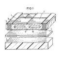
- FIG. 1 A partial area of a functional unit is shown in FIG.
- the integrated components 2 are in direct contact with their side of the cooling plate 9 facing away from the contact, which is provided with cooling channels 10. These modules 2 can either be fixed (e.g. adhesive or soldering) to the cooling plate 9, to achieve very good heat transfer, or they can only be pressed onto the latter, which facilitates the interchangeability that may be required.
- the cooling plates are provided with vias 12 on the sides. Since both the contacts for the plated-through holes and the connection contacts 1 of the integrated modules 2 lie on the same contact level, simple connection of the integrated modules 2 lying on both sides on the cooling plate 9 is possible in this way.
- micro-wiring 4 - The contacting of the integrated modules 2 with the printed circuit board 4 constructed in micro-wiring - hereinafter referred to as micro-wiring 4 - with which the wiring of the integrated modules 2 is carried out on one side in each case takes place via the contact mat 5.
- Such contact mats are already known.
- the sandwich-like structure of such a functional unit can now be continued as desired on both sides, so that a contact mat 5 and then a micro-wiring 4 comes to rest on the top of the section shown in FIG.
- a contact mat 5 then makes contact with the next component level via the microwiring 4, the components in turn being arranged on a further cooling plate.
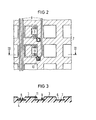
- FIG. 2 shows a plan view of the printed circuit board 4 in micro-wiring, the connections of which consist of the contact pads 3, to which the connections to the connection pads 1 of the components 2 are guided via the contact mat 5, not shown, above.
- These contact pads 3 are created by free etching on the surface of the printed circuit boards 4. Between these contact pads 3 there are then depressions 6, e.g. etched with laser, which extend to the nearest metal layer 7. This metal layer 7 is at zero volt potential. On this metal layer 7, the direct wiring 8 is laid on the zero volt level between the component connections in order to achieve a controlled characteristic impedance. At this lower level, the change wiring is contacted to etched-off contact pads 13. The electrical connection of these contact pads 13 to the component connection pads 3 takes place via the parallel vias 11.
- FIG. 3 A cross section in FIG. 3 shows the contact pads 3 and the provided depressions 6, in which the discrete wiring can run, as well as the plated-through holes 11 and the zero volt metal surface 7.
Abstract
Description
Die Erfindung betrifft ein Einbausystem für elektrische Funktionseinheiten, insbesondere der Datentechnik, bestehend aus einer wechselnden Folge von mit Kühlkanälen für ein Kühlmittel und mit Durchkontaktierungen versehenen Kühlplatten und von in Mikroverdrahtungstechnik aufgebauten Leiterplatten, die an ihren beiden Oberflächen Kontaktflächen (Kontaktpads) zur Kontaktierung mit den Anschlußkontaktflächen (Anschlußpads) von integrierten Bauelementen aufweisen, die ihrerseits mit ihrer nicht mit Anschlußpads versehenen Seite an den Kühlplatten anliegen und bei dem den Funktionseinheiten die Betriebs- und Signalspannungen von außen über Stecker zugeführt sind.The invention relates to an installation system for electrical functional units, in particular data technology, consisting of an alternating sequence of cooling plates provided with cooling channels for a coolant and with plated-through holes and of printed circuit boards constructed in micro-wiring technology, the contact surfaces (contact pads) on their two surfaces for contacting the connection contact surfaces Have (connection pads) of integrated components, which in turn rest with their side not provided with connection pads on the cooling plates and in which the operating and signal voltages are supplied to the functional units from the outside via plugs.
In vielen Bereichen der Elektrotechnik, so beispielsweise in der Datentechnik werden, wegen der zunehmenden Zahl von Schaltfunktionen pro Raumeinheit, z.B. bei integrierten Schaltkreisen, auch immer höhere Anforderungen an den konstruktiven Teil von elektronischen Geräten gestellt. Die Zuführung zahlreicher Leitungen auf immer kleinerem Raum und die Ableitung der auftretenden Wärme sind dabei wesentliche zu berücksichtigende Faktoren.In many areas of electrical engineering, for example in data technology, due to the increasing number of switching functions per room unit, e.g. With integrated circuits, ever increasing demands are placed on the structural part of electronic devices. The supply of numerous lines in an ever smaller space and the dissipation of the heat occurring are important factors to be taken into account.
Eine Bauweise, die dabei hohen Anforderungen im vorstehend genannten Sinne gerecht wird, ist bereits aus der europäischen Patentschrift 113 794 bekannt. Dort werden die mit Bauelementen, insbesondere chipsbestückten mehrlagigen Leiterplatten nebeneinander in einer Ebene in einem mit entsprechenden Ausnehmungen versehenen Gitterrahmen angeordnet, wobei jede dieser Leiterplatten eine eigene, aus gut wärmeableitendem Material bestehende Kühlplatte auf der bauteiletragenden Seite der Leiterplatte zugeordnet ist. Zusätzlich sorgt eine, sämtliche Einzelkühlplatten kontaktierende gemeinsame, mit Kühlmittel durchflossene weitere Leiterplatte für die Ableitung der den Einzelkühlplatten von den Leiterplatten zugeführten Wärme. Die Verbindung der Leiterplatten mit einer rückseitig an den Gitterrahmen angebrachten Verdrahtungsplatte wird über Andrucksteckverbinder hergestellt, die sich auf der Rückseite der Leiterplatten befinden. Diese planare Anordnung von Flachbaugruppen hat gegenüber den Vorgängersystemen, in denen auf einer Platterplatte mehrere Flachbaugruppen senkrecht zu dieser nebeneinander aufgesteckt wurden, zu einer erheblichen Verdichtung des Raum-Leistungsverhältnisses geführt, läßt jedoch eine weitere Steigerung nur noch in begrenztem Rahmen zu.A design that meets high requirements in the sense mentioned above is already known from European patent specification 113 794. There, the multi-layer printed circuit boards with components, in particular chips, are arranged side by side on one level in a grid frame provided with corresponding recesses, each of these printed circuit boards being assigned its own cooling plate, which is made of good heat-dissipating material, on the component-carrying side of the printed circuit board. In addition, a common circuit board through which coolant flows and which contacts all the individual cooling plates ensures that the heat supplied to the individual cooling plates is dissipated from the circuit boards. The connection of the printed circuit boards with a wiring plate attached to the back of the lattice frame is made using pressure connectors that are located on the back of the printed circuit boards. This planar arrangement of printed circuit boards has led to a considerable compression of the room performance ratio compared to the previous systems, in which several printed circuit boards were plugged next to each other on a flat plate, but only allowed a further increase to a limited extent.
Um eine weitere Steigerung der Packungsdichte von hochintegrierten Bauteilen zu ermöglichen, wurde in der deutschen Patentanmeldung P 39 35 047.9 bereits vorgeschlagen, in wechselnder Folge jeweils mehrere Flachbaugruppen und Kühlplatten flächenparallel hinter- bzw. aufeinander anzuordnen, so daß sie einen Quader bilden. Die Kühlplatten sind mit Kühlkanälen und mit dazu senkrechten Durchbrüchen versehen, in denen federnd ausgebildete Andruckkontakte für die Verdrahtung der Flachbaugruppen untereinander angeordnet sind. An den nicht mit Bauteilen bestückten Flächen der beiden äußeren Flachbaugruppen sind Steckerplatten mit Aussparungen zur Aufnahme von Leitungsstekkern für die Signalzuführung vorgesehen, wobei an den anderen beiden Seiten des Quaders Betriebsspannungen und an den dritten Seitenpaaren die Kühlmittelzuführung und die Kühlmittelbaführung für die Kühlplatten herangeführt werden. Dadurch wird eine dreidimensionale Verdrahtung innerhalb der Funktionseinheit und damit eine weitere Verdichtung von Bauelementen pro Volumeneinheit erreicht.In order to enable a further increase in the packing density of highly integrated components, it has already been proposed in German patent application P 39 35 047.9 to arrange a plurality of printed circuit boards and cooling plates in parallel behind or on top of one another, so that they form a cuboid. The cooling plates are provided with cooling channels and openings perpendicular to them, in which resilient pressure contacts for the wiring of the printed circuit boards are arranged with one another. On the surfaces of the two outer printed circuit boards that are not equipped with components, connector plates with cutouts for receiving cable plugs for the signal supply are provided, operating voltages being introduced on the other two sides of the cuboid and the coolant supply and the coolant supply for the cooling plates being introduced on the third side pairs. This achieves three-dimensional wiring within the functional unit and thus further compression of components per unit volume.
Aufgabe der vorliegenden Erfindung ist es, ein Einbausystem für elektrische Funktionseinheiten insbesondere für die Datentechnik zu schaffen, bei dem das Raum- Leistungsverhältnis weiter optimiert ist.The object of the present invention is to provide a built-in system for electrical functional units, in particular for data technology, in which the space-performance ratio is further optimized.
Zur Lösung dieser Aufgabe wird das Einbausystem derart ausgebildet, daß die Anschlußpads der integrierten Bauelemente mit den Kontaktpads der Leiterplatten über Kontaktmatten unmittelbar miteinander kontaktiert sind.To solve this problem, the installation system is designed such that the connection pads of the integrated components are in direct contact with one another with the contact pads of the printed circuit boards via contact mats.
Dadurch wird eine höchste Bauelementedichte erreicht, da die integrierten Bauelemente (Chips) Kante an Kante angeordnet werden können. Auch die Qualität der Mikroverdrahtung der Leiterplatten, mit denen die integrierten Bauelemente kontaktiert sind, wird erhöht, da keine zusätzliche Wärmebelastung durch Anlöten der Bauelemente entsteht, da durch das Verwenden der Kontaktmatten dieses Anlöten der Bausteine überflüssig wird. Zugleich wird auch der Bauelementewechsel, da keine Lötarbeiten mehr erforderlich sind, erleichtert.This achieves the highest component density, since the integrated components (chips) can be arranged edge to edge. The quality of the micro-wiring of the printed circuit boards with which the integrated components are contacted is increased, since there is no additional heat load due to the soldering of the components, since the soldering of the components is unnecessary by using the contact mats. At the same time, the replacement of components is made easier since no soldering work is required.
In weiterer Ausgestaltung kann die Erfindung derart ausgestaltet sein, daß zwischen den Kontaktpads der Leiterplatten Vertiefungen bis zurnächsten Metallebene der Leiterplatte vorgesehen sind, in denen diskrete Drähte für Änderungsverdrahtungen verlegbar sind, daß die diskreten Drähte mit auf dieser nächsten Metallebene freigeätzten Anschlußflecken verbindbar sind, die wiederum über Durchkontaktierungen mit den Kontaktpads an den Leiterplattenoberflächen verbunden sind.In a further embodiment, the invention can be designed in such a way that recesses are provided between the contact pads of the printed circuit boards up to the next metal level of the printed circuit board, in which discrete wires for change wiring can be laid, that the discrete wires can be connected to connection spots etched free on this next metal level, which in turn can be connected are connected via vias to the contact pads on the printed circuit board surfaces.
Das bringt den Vorteil mit sich, daß kein zusätzlicher Raum für Diskretverdrahtung erforderlich ist, was ebenfalls die Anordenbarkeit der Chips Kante an Kante unterstützt.This has the advantage that no additional space for discrete wiring is required, which also supports the arrangement of the chips edge to edge.
Wenn man die nächste Metallebene auf Null-Volt-Potential legt, läßt sich bei der Änderungsverdrahtung ein definierter Wellenwiderstand herstellen.If the next metal level is set to zero volt potential, a defined characteristic impedance can be created with the change wiring.
Außerdem ist es vorteilhaft, daß die Anschlußpads für die integrierten Bauteile und die Anschlußstellen für die Durchkontaktierungen auf den Kühlplatten auf gleichem Niveau liegen. Dadurch kann für alle Anschlüsse eine durchgehende Kontaktmatte vewendet werden.It is also advantageous that the connection pads for the integrated components and the connection points for the plated-through holes on the cooling plates are at the same level. This means that a continuous contact mat can be used for all connections.
Befestigt man die integrierten Bauelemente fest auf den Kühlplatten, so läßt sich dadurch die Kühleffektivität weiter steigern, da kürzeste Wege von der Wärmequelle (Chip) zur Wärmesenke (Kühlplatte), die entweder als Kühlflüssigkeit Wasser oder flüssigen Stickstoff enthalten kann, hergestellt sind. Der Wärmeübergang vom integrierten Bauelement zur Kühlplatte ist wegen der unmittelbaren Montierung des Chips auf der Kühlplatte ebenfalls minimiert.If the integrated components are firmly attached to the cooling plates, the cooling effectiveness can be increased further since the shortest paths from the heat source (chip) to the heat sink (cooling plate), which can either contain water or liquid nitrogen as cooling liquid, are produced. The heat transfer from the integrated component to the cooling plate is also minimized because of the direct mounting of the chip on the cooling plate.
Bei lediglichem Andrücken der Bauelemente an die Kühlplatte durch die Kontaktmatte wird die rasche Auswechselbarkeit der Bauelemente erleichtert.By simply pressing the components onto the cooling plate through the contact mat, the rapid interchangeability of the components is facilitated.
Anhand der Ausführungsbeispiele nach den FIG 1 bis 3 wird die Erfindung näher erläutert. Es zeigen
- FIG 1 ein Explosivbild eines Teils einer Funktionseinheit,
- FIG 2 die Draufsicht auf die Kontaktseite der Mikroverdrahtung,
- FIG 3 den Schnitt 111/111 nach FIG 2.
- 1 shows an exploded view of part of a functional unit,
- 2 shows the top view of the contact side of the microwiring,
- 3 shows the section 111/111 according to FIG. 2.
In FIG 1 ist ein Teilbereich einer Funktionseinheit gezeigt. Die integrierten Bauelemente 2 liegen unmittelbar mit ihrer kontaktabgewandten Seite der Kühlplatte 9 an, die mit Kühlkanälen 10 versehen ist. Diese Bausteine 2 können entweder fest (z.B. Klebung oder Lötung) mit der Kühlplatte 9 verbunden sein, zur Erreichung eines sehr guten Wärmeübergangs oder lediglich an diese angedrückt sein, wodurch die eventuell erforderliche Austauschbarkeit erleichtert wird. An den Seiten sind die Kühlplatten mit Durchkontaktierungen 12 versehen. Da sowohl die Kontakte für die Durchkontaktierungen als auch die Anschlußkontakte 1 der integrierten Bausteine 2 auf derselben Kontaktebene liegen, ist auf diese Weise eine einfache Kontaktierung der beidseitig auf der Kühlplatte 9 liegenden integrierten Bausteine 2 möglich. Die Kontaktierung der integrierten Bausteine 2 mit der in Mikroverdrahtung aufgebauten Leiterplatte 4 - im weiteren Mikroverdrahtung 4 genannt - mit der die Verdrahtung der integrierten Bausteine 2 auf jeweils einer Seite untereinander vorgenommen wird, erfolgt über die Kontaktmatte 5. Derartige Kontaktmatten sind bereits bekannt. Der sandwichartige Aufbau einer solchen Funktionseinheit läßt sich nun beliebig nach beiden Seiten fortzusetzen, so daß auf der Oberseite des in FIG 1 dargestellten Teilstückes wieder eine Kontaktmatte 5 und anschließend eine Mikroverdrahtung 4 zu liegen kommt. Eine Kontaktmatte 5 stellt dann den Kontakt mit der nächsten Bauelementeebene über die Mikroverdrahtung 4 her, wobei die Bauelemente wiederum auf einer weiteren Kühlplatte angeordnet sind.A partial area of a functional unit is shown in FIG. The integrated
FIG 2 zeigt eine Draufsicht auf die Leiterplatte 4 in Mikroverdrahtung, deren Anschlüsse aus den Kontaktpads 3 bestehen, an die über die nicht dargestellte darüberliegende Kontaktmatte 5 die Anschlüsse an die Anschlußpads 1 der Bauelemente 2 geführt werden. Diese Kontaktpads 3 entstehen durch Freiätzung an der Oberfläche der Leiterplatten 4. Zwischen diesen Kontaktpads 3 sind dann Vertiefungen 6, z.B. mit Laser eingeätzt, die bis zur nächstliegenden Metallschicht 7 reichen. Diese Metallschicht 7 liegt auf Null-Volt Potential. Auf dieser Metallschicht 7 wird zwischen den Bauelementeanschlüssen die Direktverdrahtung 8 auf der Null-Voltebene, zur Erzielung eines kontrollierten Wellenwiderstandes verlegt. Auf dieser unteren Ebene wird die Änderungsverdrahtung an freige- ätzte Kontaktflecken 13 kontaktiert. Die elektrische Verbindung dieser Kontaktflecken 13 zu den Bausteinanschlußpads 3 erfolgt über die parieellen Durchkontaktierungen 11.2 shows a plan view of the printed circuit board 4 in micro-wiring, the connections of which consist of the
Ein Querschnitt zeigt in FIG 3 die Kontaktpads 3 und die vorgesehenen Vertiefungen 6, in denen die Diskretverdrahtung verlaufen kann, sowie die Durchkontaktierungen 11 und die Null-Volt Metallfläche 7.A cross section in FIG. 3 shows the
Claims (6)
Priority Applications (1)
| Application Number | Priority Date | Filing Date | Title |
|---|---|---|---|
| AT9191111843T ATE105458T1 (en) | 1990-08-03 | 1991-07-16 | INSTALLATION SYSTEM FOR ELECTRICAL FUNCTIONAL UNITS, ESPECIALLY FOR DATA TECHNOLOGY. |
Applications Claiming Priority (2)
| Application Number | Priority Date | Filing Date | Title |
|---|---|---|---|
| DE4024737 | 1990-08-03 | ||
| DE4024737 | 1990-08-03 |
Publications (2)
| Publication Number | Publication Date |
|---|---|
| EP0471982A1 true EP0471982A1 (en) | 1992-02-26 |
| EP0471982B1 EP0471982B1 (en) | 1994-05-04 |
Family
ID=6411624
Family Applications (1)
| Application Number | Title | Priority Date | Filing Date |
|---|---|---|---|
| EP91111843A Expired - Lifetime EP0471982B1 (en) | 1990-08-03 | 1991-07-16 | Mounting system for electrical function units, especially for data technics |
Country Status (5)
| Country | Link |
|---|---|
| US (1) | US5153814A (en) |
| EP (1) | EP0471982B1 (en) |
| JP (1) | JPH088423B2 (en) |
| AT (1) | ATE105458T1 (en) |
| DE (1) | DE59101555D1 (en) |
Cited By (1)
| Publication number | Priority date | Publication date | Assignee | Title |
|---|---|---|---|---|
| EP0762818A2 (en) * | 1995-09-11 | 1997-03-12 | International Business Machines Corporation | Device for manufacturing a connection to a circuit board |
Families Citing this family (16)
| Publication number | Priority date | Publication date | Assignee | Title |
|---|---|---|---|---|
| DE59503218D1 (en) * | 1994-02-07 | 1998-09-24 | Siemens Ag | Method for producing a cubic integrated circuit arrangement |
| US6281042B1 (en) | 1998-08-31 | 2001-08-28 | Micron Technology, Inc. | Structure and method for a high performance electronic packaging assembly |
| US6392296B1 (en) | 1998-08-31 | 2002-05-21 | Micron Technology, Inc. | Silicon interposer with optical connections |
| US6586835B1 (en) * | 1998-08-31 | 2003-07-01 | Micron Technology, Inc. | Compact system module with built-in thermoelectric cooling |
| US6219237B1 (en) * | 1998-08-31 | 2001-04-17 | Micron Technology, Inc. | Structure and method for an electronic assembly |
| US6255852B1 (en) | 1999-02-09 | 2001-07-03 | Micron Technology, Inc. | Current mode signal interconnects and CMOS amplifier |
| US7554829B2 (en) | 1999-07-30 | 2009-06-30 | Micron Technology, Inc. | Transmission lines for CMOS integrated circuits |
| US6464513B1 (en) * | 2000-01-05 | 2002-10-15 | Micron Technology, Inc. | Adapter for non-permanently connecting integrated circuit devices to multi-chip modules and method of using same |
| US6407566B1 (en) | 2000-04-06 | 2002-06-18 | Micron Technology, Inc. | Test module for multi-chip module simulation testing of integrated circuit packages |
| US6540525B1 (en) * | 2001-08-17 | 2003-04-01 | High Connection Density, Inc. | High I/O stacked modules for integrated circuits |
| US7045889B2 (en) * | 2001-08-21 | 2006-05-16 | Micron Technology, Inc. | Device for establishing non-permanent electrical connection between an integrated circuit device lead element and a substrate |
| US7049693B2 (en) * | 2001-08-29 | 2006-05-23 | Micron Technology, Inc. | Electrical contact array for substrate assemblies |
| US7101770B2 (en) | 2002-01-30 | 2006-09-05 | Micron Technology, Inc. | Capacitive techniques to reduce noise in high speed interconnections |
| US7235457B2 (en) | 2002-03-13 | 2007-06-26 | Micron Technology, Inc. | High permeability layered films to reduce noise in high speed interconnects |
| DE10229711B4 (en) * | 2002-07-02 | 2009-09-03 | Curamik Electronics Gmbh | Semiconductor module with microcooler |
| US7432592B2 (en) * | 2005-10-13 | 2008-10-07 | Intel Corporation | Integrated micro-channels for 3D through silicon architectures |
Citations (5)
| Publication number | Priority date | Publication date | Assignee | Title |
|---|---|---|---|---|
| GB1178566A (en) * | 1966-06-13 | 1970-01-21 | Ibm | Improvements in and relating to Electronic Circuit Packages |
| EP0113794A1 (en) * | 1982-12-21 | 1984-07-25 | Siemens Aktiengesellschaft | Support for component parts |
| EP0268260A1 (en) * | 1986-11-18 | 1988-05-25 | International Business Machines Corporation | Flexible film chip carrier with decoupling capacitors |
| US4933808A (en) * | 1989-05-11 | 1990-06-12 | Westinghouse Electric Corp. | Solderless printed wiring board module and multi-module assembly |
| EP0428859A2 (en) * | 1989-10-20 | 1991-05-29 | Siemens Nixdorf Informationssysteme Aktiengesellschaft | Eletric functional unit for data processing |
Family Cites Families (11)
| Publication number | Priority date | Publication date | Assignee | Title |
|---|---|---|---|---|
| DE428859C (en) * | 1925-07-06 | 1926-05-14 | Eberhard Legeler Dr | Process for the continuous separation of sulfur from sulfur solutions |
| US4016138A (en) * | 1973-02-08 | 1977-04-05 | Michigan Chemical Corporation | Plastic compositions |
| US4060113A (en) * | 1974-07-03 | 1977-11-29 | Ryuzo Matsushima | Tightening device for threaded screw part |
| US4019098A (en) * | 1974-11-25 | 1977-04-19 | Sundstrand Corporation | Heat pipe cooling system for electronic devices |
| US4037270A (en) * | 1976-05-24 | 1977-07-19 | Control Data Corporation | Circuit packaging and cooling |
| US4597617A (en) * | 1984-03-19 | 1986-07-01 | Tektronix, Inc. | Pressure interconnect package for integrated circuits |
| EP0204568A3 (en) * | 1985-06-05 | 1988-07-27 | Harry Arthur Hele Spence-Bate | Low power circuitry components |
| JPS6212991U (en) * | 1985-07-05 | 1987-01-26 | ||
| JPS63192256A (en) * | 1987-02-04 | 1988-08-09 | Nec Corp | Integrated circuit cooling constitution |
| US4953060A (en) * | 1989-05-05 | 1990-08-28 | Ncr Corporation | Stackable integrated circuit chip package with improved heat removal |
| US5014117A (en) * | 1990-03-30 | 1991-05-07 | International Business Machines Corporation | High conduction flexible fin cooling module |
-
1991
- 1991-07-16 AT AT9191111843T patent/ATE105458T1/en not_active IP Right Cessation
- 1991-07-16 DE DE59101555T patent/DE59101555D1/en not_active Expired - Fee Related
- 1991-07-16 EP EP91111843A patent/EP0471982B1/en not_active Expired - Lifetime
- 1991-07-18 US US07/732,482 patent/US5153814A/en not_active Expired - Fee Related
- 1991-07-29 JP JP3212655A patent/JPH088423B2/en not_active Expired - Lifetime
Patent Citations (5)
| Publication number | Priority date | Publication date | Assignee | Title |
|---|---|---|---|---|
| GB1178566A (en) * | 1966-06-13 | 1970-01-21 | Ibm | Improvements in and relating to Electronic Circuit Packages |
| EP0113794A1 (en) * | 1982-12-21 | 1984-07-25 | Siemens Aktiengesellschaft | Support for component parts |
| EP0268260A1 (en) * | 1986-11-18 | 1988-05-25 | International Business Machines Corporation | Flexible film chip carrier with decoupling capacitors |
| US4933808A (en) * | 1989-05-11 | 1990-06-12 | Westinghouse Electric Corp. | Solderless printed wiring board module and multi-module assembly |
| EP0428859A2 (en) * | 1989-10-20 | 1991-05-29 | Siemens Nixdorf Informationssysteme Aktiengesellschaft | Eletric functional unit for data processing |
Cited By (2)
| Publication number | Priority date | Publication date | Assignee | Title |
|---|---|---|---|---|
| EP0762818A2 (en) * | 1995-09-11 | 1997-03-12 | International Business Machines Corporation | Device for manufacturing a connection to a circuit board |
| EP0762818A3 (en) * | 1995-09-11 | 1997-05-14 | Ibm | Device for manufacturing a connection to a circuit board |
Also Published As
| Publication number | Publication date |
|---|---|
| JPH088423B2 (en) | 1996-01-29 |
| US5153814A (en) | 1992-10-06 |
| DE59101555D1 (en) | 1994-06-09 |
| ATE105458T1 (en) | 1994-05-15 |
| EP0471982B1 (en) | 1994-05-04 |
| JPH04233795A (en) | 1992-08-21 |
Similar Documents
| Publication | Publication Date | Title |
|---|---|---|
| EP0471982B1 (en) | Mounting system for electrical function units, especially for data technics | |
| DE1591199C2 (en) | ||
| DE4015788C2 (en) | Assembly | |
| AT398254B (en) | CHIP CARRIERS AND ARRANGEMENT OF SUCH CHIP CARRIERS | |
| DE10240730B4 (en) | Printed circuit board, memory module and manufacturing process | |
| DE3805851C2 (en) | ||
| CH667562A5 (en) | PROCEDURE FOR MODIFYING A FLAT ELECTRICAL ASSEMBLY. | |
| DE4305793A1 (en) | Power module | |
| DE2843710A1 (en) | MULTI-LAYER FLEXIBLE CIRCUIT BOARD ARRANGEMENT AND METHOD OF MANUFACTURING IT | |
| EP0106990A1 (en) | Contacting element for printed circuit boards | |
| DE69929337T2 (en) | PRINTED PCB PLATE UNIT, HIERARCHICAL ASSEMBLY ASSEMBLY AND ELECTRONIC APPARATUS | |
| DE69936189T2 (en) | ELECTRIC CONDUCTOR WITH FLANGED AND GROOVED CROPS SHAPED SURFACE STRUCTURE | |
| DE3935047C2 (en) | ||
| DE3212592A1 (en) | Cooling device for information technology apparatuses | |
| EP0153990A1 (en) | Flat module | |
| DE3330466A1 (en) | HIGH PACKING DENSITY ARRANGEMENT OF INTEGRATED CIRCUITS | |
| DE19805492C2 (en) | Circuit board | |
| DE102016101757A1 (en) | CIRCUIT MODULE WITH SURFACE MOUNTABLE SURFACE BLOCKS FOR CONNECTING A PCB | |
| DE60201537T2 (en) | ELECTRICAL CONNECTION ARRANGEMENT FOR ELECTRONIC COMPONENTS | |
| DE2929050A1 (en) | MULTILAYER PRINTED CIRCUIT BOARD AND METHOD FOR SIZING IT | |
| EP0238712A1 (en) | Controlled commutator matrix | |
| EP0073489A2 (en) | Electrical module | |
| DE3209699C2 (en) | Universal circuit board | |
| DE2815646A1 (en) | Support assembly for circuit boards - has boards held by frame to form hollow cube with corner connections and internal heat sink | |
| DE3134385A1 (en) | Electrical assembly having a plurality of parallel printed circuit boards |
Legal Events
| Date | Code | Title | Description |
|---|---|---|---|
| PUAI | Public reference made under article 153(3) epc to a published international application that has entered the european phase |
Free format text: ORIGINAL CODE: 0009012 |
|
| AK | Designated contracting states |
Kind code of ref document: A1 Designated state(s): AT BE CH DE FR GB IT LI NL |
|
| 17P | Request for examination filed |
Effective date: 19920325 |
|
| 17Q | First examination report despatched |
Effective date: 19930818 |
|
| GRAA | (expected) grant |
Free format text: ORIGINAL CODE: 0009210 |
|
| AK | Designated contracting states |
Kind code of ref document: B1 Designated state(s): AT BE CH DE FR GB IT LI NL |
|
| REF | Corresponds to: |
Ref document number: 105458 Country of ref document: AT Date of ref document: 19940515 Kind code of ref document: T |
|
| REF | Corresponds to: |
Ref document number: 59101555 Country of ref document: DE Date of ref document: 19940609 |
|
| PGFP | Annual fee paid to national office [announced via postgrant information from national office to epo] |
Ref country code: BE Payment date: 19940714 Year of fee payment: 4 |
|
| PGFP | Annual fee paid to national office [announced via postgrant information from national office to epo] |
Ref country code: FR Payment date: 19940725 Year of fee payment: 4 |
|
| ITF | It: translation for a ep patent filed |
Owner name: STUDIO JAUMANN |
|
| PGFP | Annual fee paid to national office [announced via postgrant information from national office to epo] |
Ref country code: NL Payment date: 19940731 Year of fee payment: 4 |
|
| GBT | Gb: translation of ep patent filed (gb section 77(6)(a)/1977) |
Effective date: 19940711 |
|
| ET | Fr: translation filed | ||
| PGFP | Annual fee paid to national office [announced via postgrant information from national office to epo] |
Ref country code: DE Payment date: 19940915 Year of fee payment: 4 |
|
| PGFP | Annual fee paid to national office [announced via postgrant information from national office to epo] |
Ref country code: CH Payment date: 19941017 Year of fee payment: 4 |
|
| PLBE | No opposition filed within time limit |
Free format text: ORIGINAL CODE: 0009261 |
|
| STAA | Information on the status of an ep patent application or granted ep patent |
Free format text: STATUS: NO OPPOSITION FILED WITHIN TIME LIMIT |
|
| 26N | No opposition filed | ||
| PGFP | Annual fee paid to national office [announced via postgrant information from national office to epo] |
Ref country code: GB Payment date: 19950622 Year of fee payment: 5 |
|
| PGFP | Annual fee paid to national office [announced via postgrant information from national office to epo] |
Ref country code: AT Payment date: 19950628 Year of fee payment: 5 |
|
| PG25 | Lapsed in a contracting state [announced via postgrant information from national office to epo] |
Ref country code: LI Effective date: 19950731 Ref country code: CH Effective date: 19950731 Ref country code: BE Effective date: 19950731 |
|
| BERE | Be: lapsed |
Owner name: SIEMENS NIXDORF INFORMATIONSSYSTEME A.G. Effective date: 19950731 |
|
| PG25 | Lapsed in a contracting state [announced via postgrant information from national office to epo] |
Ref country code: NL Effective date: 19960201 |
|
| REG | Reference to a national code |
Ref country code: CH Ref legal event code: PL |
|
| NLV4 | Nl: lapsed or anulled due to non-payment of the annual fee |
Effective date: 19960201 |
|
| PG25 | Lapsed in a contracting state [announced via postgrant information from national office to epo] |
Ref country code: DE Effective date: 19960402 |
|
| PG25 | Lapsed in a contracting state [announced via postgrant information from national office to epo] |
Ref country code: FR Effective date: 19960430 |
|
| REG | Reference to a national code |
Ref country code: FR Ref legal event code: ST |
|
| REG | Reference to a national code |
Ref country code: FR Ref legal event code: ST |
|
| REG | Reference to a national code |
Ref country code: FR Ref legal event code: ST |
|
| PG25 | Lapsed in a contracting state [announced via postgrant information from national office to epo] |
Ref country code: GB Effective date: 19960716 Ref country code: AT Effective date: 19960716 |
|
| GBPC | Gb: european patent ceased through non-payment of renewal fee |
Effective date: 19960716 |
|
| PG25 | Lapsed in a contracting state [announced via postgrant information from national office to epo] |
Ref country code: IT Free format text: LAPSE BECAUSE OF NON-PAYMENT OF DUE FEES;WARNING: LAPSES OF ITALIAN PATENTS WITH EFFECTIVE DATE BEFORE 2007 MAY HAVE OCCURRED AT ANY TIME BEFORE 2007. THE CORRECT EFFECTIVE DATE MAY BE DIFFERENT FROM THE ONE RECORDED. Effective date: 20050716 |