EP0478148B1 - Work station including a direct memory access controller - Google Patents
Work station including a direct memory access controller Download PDFInfo
- Publication number
- EP0478148B1 EP0478148B1 EP91307975A EP91307975A EP0478148B1 EP 0478148 B1 EP0478148 B1 EP 0478148B1 EP 91307975 A EP91307975 A EP 91307975A EP 91307975 A EP91307975 A EP 91307975A EP 0478148 B1 EP0478148 B1 EP 0478148B1
- Authority
- EP
- European Patent Office
- Prior art keywords
- bus
- unit
- data
- operational
- internal transaction
- Prior art date
- Legal status (The legal status is an assumption and is not a legal conclusion. Google has not performed a legal analysis and makes no representation as to the accuracy of the status listed.)
- Expired - Lifetime
Links
Images


Classifications
-
- G—PHYSICS
- G06—COMPUTING; CALCULATING OR COUNTING
- G06F—ELECTRIC DIGITAL DATA PROCESSING
- G06F13/00—Interconnection of, or transfer of information or other signals between, memories, input/output devices or central processing units
- G06F13/38—Information transfer, e.g. on bus
- G06F13/40—Bus structure
- G06F13/4004—Coupling between buses
- G06F13/4027—Coupling between buses using bus bridges
- G06F13/405—Coupling between buses using bus bridges where the bridge performs a synchronising function
Landscapes
- Engineering & Computer Science (AREA)
- General Engineering & Computer Science (AREA)
- Theoretical Computer Science (AREA)
- Computer Hardware Design (AREA)
- Physics & Mathematics (AREA)
- General Physics & Mathematics (AREA)
- Bus Control (AREA)
Description
- This invention relates to a work station or similar data processing system. More particularly, the invention relates to an architecture for such data processing system.
- An architectural feature of many data processing systems is a direct memory access (DMA) controller.
- A DMA controller is provided with CPU-type logic and is dedicated to the task of moving data between system memory and an external system bus providing communication with input/output devices. A typical DMA controller is connected to the external bus and includes the logic necessary to compensate for different operating frequencies of the external bus and system memory. For example, in a system having an external Micro Channel bus, a DMA controller may be connected to a slot on the Micro Channel.
- This type of DMA controller includes logical circuitry and memories for handling data transfer, including compensation for timing and frequency differences between the CPU clock and the Micro Channel clock. Inherently, this known DMA controller is an extremely complex unit with its operation considerably influencing the overall performance of the system.
- It is an object of the present invention to provide a work station having improved performance.
- It is a further object of the present invention
- From US-A-4744078 there is known a data transfer controller for transferring data from a network bus operating at a first clock frequency to a system bus operating at a second clock frequency. The controller includes an internal transaction bus, a local memory, a direct access channel which handles the transfer of data to and from the local memory, and first and second interfacing units between the internal transaction bus and the network and system buses respectively, the second interfacing unit including sysnchronizing means.
- EP-A-0343770 discloses a work station having an interface for connecting a system bus and a Micro Channel bus, a DMA controller being connected to the system bus.
- It is an object of the present invention to provide a work station having improved performance.
- It is a further object of the present invention to provide a work station including a simplified DMA controller compared with a known type of DMA controller.
- According to the invention there is provided a work station including a central processing unit operating with a first clock frequency, main memory means, a first bus to which are connected said central processing unit and said main memory means, and a second bus operating with a second clock frequency, different from said first clock frequency, characterized by an interface chip connected between said first bus and said second bus, said interface chip including an internal transaction bus, a first operational unit comprising a DMA controller for controlling data transfer between said first bus and said second bus and for controlling data transfer from said second bus to said main memory means without control by said central processing unit, a second operational unit comprising a first interfacing unit between said internal transaction bus and said first bus, a third operational unit comprising a second interfacing unit between said internal transaction bus and said second bus, said second interfacing unit including synchronizing means for compensating for the difference between said first and second clock frequencies, and data being arranged to be transferred between said first, second and third operational units over said internal transaction bus at said first clock frequency, and internal arbiter means for granting either said DMA controller or one of said second and third operational units access to said internal transaction bus.
- Thus, the functionality of the DMA controller and sysnchronizer are separated. In this manner, the DMA design is simplified and can be reused in similar designs having different timing requirements between the first and second buses.
- In a preferred embodiment of the present invention, the internal transaction bus enables communication between the individual operational units. Each operational unit has an identification number by which it is addressable over specific lines of the internal transaction bus. An internal arbiter grants access to the internal transaction bus to a unit having highest priority. The internal transaction bus operates independently of the first bus but with the same frequency as the central processing unit.
- It should be understood that the splitting of the functions between the DMA controller and the synchronizing means in a work station according to the invention provides a smooth data transfer through a compact and effectively controlled interface chip.
- One embodiment of the invention will now be described by way of example with reference to the accompanying drawings, in which:-
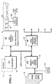
- Fig. 1 is a schematic overall view of one embodiment of a work station according to the invention illustrating the various functional blocks of the work station and the connections therebetween;
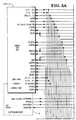
- Figs. 2A to 2E, arranged as shown in Fig. 2, are a schematic drawing showing in detail a host P/M bus as used to connect the various functional blocks with each other;
- Fig. 3 is a block diagram of a bus interface block BIB;
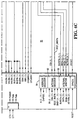
- Figs. 4A to 4D, arranged as shown in Fig. 4, are a schematic drawing showing in detail the various lines of an internal transaction bus of the BIB;
- Figs. 5A and 5B are a block diagram of a synchronizer used in the BIB;
- Fig. 6 is a schematic drawing illustrating the principal design of a buffer used with the synchronizer of Figs. 5A and 5B; and
- Fig. 7 is a timing diagram used for explaining operation of the work station for a single write cycle.
- Fig. 1 shows a preferred embodiment of a work station or data processing system according to the invention.
- Basically, a
CPU 10 communicates through a host P/M bus 20 withfunctional blocks - It should be noted that different types of microprocessors may be used for the
CPU 10, such as the Intel 80386, 80386SX, and 80486 microprocessors. Also, acoprocessor 12, such as a mathematical coprocessor Intel 80387, or 80387SX may be added. - The functional block BIB 30 is provided as an interface between the host P/
M bus 20 and a Micro Channel 32 provided with a plurality of slots 32a for attaching conventional input/output devices including adapter boards provided with a microprocessor which may act as a master in communication with other functional blocks of the work station. Also, an example of an adapter board is a circuit board carrying additional memory. Furthermore, a control 32b is connected to the Micro Channel 32 for controlling a fixed disk drive. - The
functional block MIB 40 forms an interface between the host P/M bus 20 and aDRAM memory 42 which may have different sizes with a presently usual size of 16 MB up to 64 MB. Furthermore, theMIB 40 controls access to the usual BIOS ROM memory 42a. - The functional peripheral interface block PIB 50 (Fig. 1) forms an interface between the host P/
M bus 20 and various conventional system and peripheral units through respective control blocks. All these units are well known in the art, and therefore they will not be described in further detail. - Each of the functional blocks BIB 30, MIB 40 and
PIB 50 has been specifically designed as one microchip each containing all elements such as registers and logic circuitry necessary to establish and perform communication between the host P/M bus 20 and the individual units connected to eachfunctional block - As indicated in Fig. 1 it should be noted that a plurality m of
BIBs 30 and a plurality n ofMIBs 40 may be provided all connected to the host P/M bus 20. Thus, a large variety of configurations with different CPUs and different memory capacities may be implemented. Each chip may be configured quite differently to match various configurations of the system. - Each
functional block BIB 30 and anMIB 40, and of many other procedures. As regards theMIBs 40, these blocks will organize refresh cycles for the DRAMs and overflow cleaning of caches included therein. - Basically, each
functional block - Specifically referring to Fig. 3, the bus interface block BIB 30 shown therein comprises, preferably arranged on one microchip, a host P/M bus interface HPI 34 forming an interface between the host P/
M bus 20 and aninternal transaction bus 35 providing communication connections to an EMCAunit 38, which is an interfacing unit to at least one Micro Channel. The EMCAunit 38 includes a synchronizing unit SYNC 37 which is connected to an extended MCA bus controller orMCA unit 39 for access to the Micro Channel 32. Further details of the EMCAunit 38 will be explained hereafter in connection with Figs. 5A and 5B. - Further connected to the
internal transaction bus 35 is aDMA controller DMA 36 for controlling data transfer between aDRAM memory 42 and the Micro Channel 32 via anMIB 40 and the host P/M bus 20. - The work station offers high flexibility in respect of using one of various types of CPUs and a plurality of Micro Channels and DRAM memory units to be included in the system. This is in contrast with known work stations where a predetermined CPU communicates with one Micro Channel and one DRAM memory block only.
- A specifically extended host P/M bus is illustrated in Figs. 2A-2E in detail. Specifically, within the
block CPU 10 the conventional input/output ports of a microprocessor, such as Intel 80386, etc., are listed as address ports A(2,...31), data ports D(0,...31), byte enable ports BEb (0,...3), and an address status output ADSb which indicates that a valid bus cycle definition and address are available and which is driven active in the same clock as the addresses are driven. ADSb is active low. The system clock PCLK is generated by aclock oscillator 60 and supplied to the input port PCLK of theCPU 10 and thefunctional blocks BIB 30,MIB 40, andPIB 50. These and all other input/output ports of theCPU 10 and the signals presented there are conventional. Thus, they will not be explained in detail. - As may be gathered from Figs. 2A-2E, the
functional blocks BIB 30,MIB 40, andPIB 50 are provided with similar input/output ports as the CPU. However, there are several additional ports and associated bus lines connecting corresponding ports of the functional blocks and the CPU with each other such as CT (0..1) which is a combination of the two lines included in the host P/M bus indicating the type of processor (or functional block) which has access to the host P/M bus. BREQb (0...3) is a host P/M bus request signal with the assumption that fourBIBs 30 may be provided
each being connected with thePIB 50 by one request line. BGNTb (0..3) is a host P/M bus grant signal transmitted by thePIB 50 to one of theBIBs 30 having requested access to the host P/M bus by BREQb (0...3). SBURSTBLb is a signal generated by one of thefunctional blocks BIB 30 to temporarily halt the transfer in burst mode but keeping the burst condition established. CIN and COUT are input/output signals used in a system configuration routine. - Particularly referring to Figs 3 and Figs. 4A-4D, the specific design of one functional block will be explained taking a
BIB 30 as an example. - As mentioned before, the
functional block BIB 30 basically comprisesunit HPI 34,DMA controller 36,SYNC unit 37, andMCA unit 39, which according to Figs. 4A-4D is actually combined withEMCA unit 38. These three units communicate with each other through the internaltransaction bus TRACT 35 in a similar manner as theCPU 10 and thefunctional blocks BIB 30,MIB 40, andPIB 50. - Accordingly, the
BIB 30 is a self-contained functional block performing several functions without control of theCPU 10 or another busmaster. - A comparison of Figs. 4A-4D with Figs. 2A-2E shows close similarities of the signals and corresponding lines on the host P/M bus and
internal transaction bus 35. - Each
unit TRACT bus 35 has a VALID signal, a REQUEST signal, a GRANT signal, and a BURST signal. Each unit has an ID number according to priority with "0" the highest priority. Specifically,EMCA 38 has assigned #0,DMA 36 has assigned #1, andHPI 34 has assigned #2. - In the following Table 1 the main signals of
TRACT 35 are listed.

- Referring particularly to Fig. 4C,
HPI 34 includes aninternal decoder 62 which uses the IA2 to IA31 lines to decode the access to the individual units. Every unit has its own address decode signal. This signal is generated for both memory or I/O accesses and all other commands a unit may receive. Also, theinternal decoder 62 receives the busy signals of all units such asDMA 36 andEMCA 38 and generates the DEST-BUSYb signal. - Furthermore, the
address decoder 64 is provided for receiving the address signals A2 to A31 from the host P/M bus 20 (see Figs. 2 and 3) and generates the CHIPSEL signal indicating that the corresponding functional block such asBIB 30 has been selected for communication through the host P/M bus 20. - Of particular interest is the
internal arbiter 66 included in theHPI 34. To get access to theTRACT 35, a unit such asHPI 34,DMA 36, andEMCA 38 has to assert a request by generating a request signal REQb (0..2) toTRACT 35. Several requests may occur simultaneously. Thus, it is the task of theinternal arbiter 66 to resolve these requests and to generate a grant signal GNTb (0..2) for the requesting unit with the highest priority. As mentioned before, in thepreferred embodiment EMCA 38 has the highest priority "0" while theHPI 34 has the lowest priority "2". The unit which detects its grant signal at the rising edge of the clock has access to theTRACT 35 for the next cycle. - Another task of the
internal arbiter 66 is to handle a burst mode in which there are transmitted a plurality of data words preceded by a single address word. If a unit has detected its grant signal and wishes to carry out multiple data transfers on theTRACT 35, then this unit activates its burst line. For example, ifEMCA 38 has requested access to theTRACT 35 by signal REQb(0) and has received access by theinternal arbiter 66 transmitting the grant signal GNTb(0) to theEMCA 38, the latter will generate its BURSTb(0) signal for multiple data transfer. When the burst line is activated, the current grant is kept active regardless of requests of any other unit for bus access. Also, theinternal arbiter 66 receives the RETRYb(0...2) signals of all units and uses them for reordering the priority for the next cycle. - It should be mentioned that on the
TRACT 35 all cycles are synchronous with the clock PCLK on the host P/M bus 20. All clock dependent timing is based on the rising edge of PCLK. This means that the action which refers to PCLK occurs after the next rising edge. That unit, such asDMA controller 36, initiating a cycle on theTRACT 35 is called "master". Therefore, some of the control signals generated by a "master" are preceded by "M". The unit responding to that cycle is called "slave". Thus, some signals generated by a "slave" are preceded by "S". For example, with theDMA 36 requesting data transfer from theMicro Channel 32 to theDRAMs 42 through host P/M bus 20 andMIB 40 theDMA 36 initiates a corresponding cycle on theTRACT 35 for internal communication withHPI 34. A "b" at the end of a signal name means that this signal is active low. - In Figs. 4A-4D some of the lines of the internal transaction bus, i.e.
TRACT 35, have assignments starting with "I" such as IA(2..31) or ID(0..31) in order to distinguish them from similar lines of the host P/M bus 20 such as A(2:31) or D(0..31) for addresses and data, respectively. - Prior to entering into a detailed description of the synchronizer according to the invention it appears useful to briefly indicate the operation within the
BIB 30 for a single write cycle as an example. - Basically, it is assumed that the
DMA 36 wishes to write data from a Micro Channel device to theDRAMs 42 which is accomplished through the host P/M bus 20 andMIB 40. However, in order to get access to the host P/M bus 20, the address and data are transmitted toHPI 34 forming the interface to the host P/M bus 20 (see Fig. 3). - Write cycles consist of one transfer on the
TRACT 35 only. A valid address, data, and command are issued on theTRACT 35 at the same time. - In Fig. 7, line (a) represents the CPU clock PCLK governing the timing of all cycles to be performed. As a first action according to line (b),
DMA 36 generates the M-REQb signal going active low which signal is transmitted to the internal arbiter 66 (Fig. 6) which after arbitration returns the M-GNTb signal toDMA 36 according to line (c). - As may be seen from line (d) the following information is presented simultaneously, i.e. in parallel on the lines of TRACT 35: an address IA on address lines IA2 to IA31; data ID(0..31) on lines ID0 to ID31; the unit identification number IDN on two lines IDN(0:1), i.e. for the present example "01" for the
DMA 36; and a command IC, specifically on lines IC0, IC1, and IC2 indicating a memory or I/O data write access. - A comparison of lines (d) and (g) of Fig. 7 indicates that
DMA 36 generates a M-VALIDb signal for the time the information according to line (d) is presented onTRACT 35. Every unit has a valid line. This line is activated when the master unit detects a GRANT and puts valid address, data, and command on theTRACT 35. As long as address, data, and command are valid the VALIDb signal is active. - A VALIDb signal can be activated even if the receiving unit is currently busy. In this case the
TRACT 35 and the valid signal have to remain activated until the receiving unit resets its BUSY line. Then the master can deactivate VALIDb and release theTRACT 35 on the next rising edge. The signal M-BURSTb according to line (e) inactive high indicates the situation that no burst mode operation is intended. Line (f) illustrates the S-BUSYb signal going active low generated by theHPI 34 as a slave indicating the taking-over of the information according to line (d) for presenting it to the host P/M bus 20 independent of the further operation within theBIB 30. Every unit has its own busy line. The busy line is used to tell other units that a unit can not accept a new command. - BUSYb is activated only if a unit has received a command which requires more than one clock cycle to be finished. In this case busy is activated immediately on the rising clock edge after a unit received a valid command.
- As long as a unit's BUSYb is deactivated the unit is able to accept a new command from the
TRACT 35 on the next rising edge of the clock. Busy is deactivated one clock before completion of the command. - As regards the situation illustrated in the right-hand part of Fig.. 7, this differs from that illustrated in the left-hand part in that there is a delay due to the fact that the address slave unit, i.e.
HPI 34, is busy in the current TRACT bus cycle. Accordingly, the signals illustrated in the lines (b), (c), (d), and (g) are extended until the DEST-BUSYb signal, line (h) generated from theinternal decoder 62 of theHPI 34 and indicating the busy signal goes inactive high again. - With the M-RETRYb signal according to line (i),
DMA 36 may influence theinternal arbiter 66 to rearrange priority. - Referring now specifically to Figs. 3, 4A-4D, and 5A-5B, there will be explained further details of the
EMCA unit 38 which is specifically designed according to the invention. - Basically, the
EMCA unit 38 incorporates the logic to interface the internaltransaction bus TRACT 35 of theBIB 30 with the extendedMicro Channel bus 32. Thus, theEMCA unit 38 generates a CPU independent timing for theMicro Channel 32. - Figs. 5A and 5B show the
synchronizer 37 of the preferred embodiment of the invention in more detail. Specifically, it should be understood that thesynchronizer 37 interfaces the internal transaction bus TRACT 35 (left-hand side of Fig. 5A) of the BIB 30 (Figs. 3 and 4) with the MCA unit 39 (right-hand side). - The main function of the
synchronizer 37 is to compensate for the different operating frequencies of theCPU 10 and theMicro Channel 32, and to buffer data in order to smooth data transfer, and enhance the flexibility of the system. - Specifically, the
synchronizer 37 synchronizes transfers between theMCA unit 39 and the internaltransaction bus TRACT 35 of theBIB 30. This is particularly necessary since theMCA unit 39 is clocked at 40 MHz, regardless of the CPU frequency which may operate at varying frequencies between 20 MHz and 33 MHz, for example. In addition, thesynchronizer 37 provides buffering of EMCA streaming data which means data transmitted at a very fast data rate of up to 80 MB/second in blocks of 64 bits. This is done by abuffer 70 comprising eight registers each having a width of 68 (64 + 4) bits. - As will now be explained, the
synchronizer 37 includes four internal bus pairs. All the signals entering or leaving thesynchronizer SYNC 37 are buffered. Some of these buffers are constantly enabled. - As may be seen on the left-hand side of Fig. 5A, the address bus IA(31:2) of the
TRACT 35 which is bi-directional communicates with an address bus pair split into an input address bus ain(31:2) and an output address bus aout(31:2). The input and output address buses are connected to latches Aout and Ain of theMCA unit 39. - It should be generally noted that the direction of data flow is determined by
drivers 80 driven by corresponding control signals for data input and output validbi and validbo. - Data lines ID(31:0) of the
TRACT 35 communicate via the internal bus lines dinl(31:0), doutl(31:0), and douth (31:0), partially through appropriate prestorage Eregisters 76, 78, with corresponding latches DLout, DHout, DLin, DHin of theMCA unit 39, with DL indicating the lower portion of data comprising 32 bits and DH referring to the higher portion of data of 32 bits. - The IBEb(3:0) lines of the
TRACT 35 for the byte enable signals communicate with the internal synchronizer bus lines bebin(3:0) and bebout(3:0) and through some additional circuitry to be explained later, such as the multiplexers MUX2 84 and 86 andfurther Eregisters MCA unit 39. - Similarly, the
TRACT 35 command bus Cout and Cin communicates through the internal synchronizer bus lines cout (10:0) and cin (12:0) and amultiplexer MUX2 93 with the corresponding latches cin and cout of theMCA unit 39. - The control portion of the
synchronizer 37 mainly comprises acontrol state machine 90 connected to theTRACT 35 control through somecombinational logic circuitry control state machine 90 are synchronizingcircuits - The control input portion of the internal synchronizer bus further includes an Eregister(12:0) 94.
- A most important unit of the
synchronizer 37 is thebuffer 70 connected to the data input lines and data output lines dinl(31:0), dinh(31:0), doutl(31:0), and douth(31:0), and to the internal byte enable lines bebin(3:0) and bebout(3:0). - It should be noted that there are two clock signals, i.e. the CPU clock NPCLK and the Micro Channel clock MCLK with the data and byte enable signals presented by the
MCA unit 39 through theprestorage registers buffer 70 clocked by the CPU clock NPCLK. Therefore, this provides an independent timing between theCPU 10 and theMicro Channel 32, independent of the operating frequency selected for theCPU 10, with usually the MCLK having a higher frequency (such as 40 MHz) than the CPU clock (between 20 MHz and 33 MHz). Thebuffer 70 has an excellent buffering capability smoothing out considerable time differences and interruptions in data transfer such that an optimum continuity is achieved. Also, thebuffer 70 provides the system with considerable flexibility. - After having explained the main structure of the
synchronizer 37, some more details will be given in respect of the function thereof. - As mentioned before, the address bus IA(31:2) of the
TRACT 35 is connected to the bi-directional internal address bus of thesynchronizer 37. The gating of the addresses is controlled by the signal called validbi which means "let addresses enter" from theTRACT 35 into theSYNC 37, and by the signal validbo which means "issue an address" on to theTRACT 35. - It should be noted that the aout bus is always connected to the MCA input latches Ain to ensure no floating inputs at the MCA inputs. The output address value of the MCA output latches Aout is gated on to the ain bus whenever no valid address is gated in from the
TRACT 35. - If a valid command is issued from the
TRACT 35 to theSYNC 37 then the address from the ain bus is stored in theEregister 72, the output of which is connected to the aout bus; hence the incoming address is passed on to the aout bus just after storing the address value in theEregister 72. - The lower two address bits aout (2) and aout (3) are multiplexed by means of a
multiplexer MUX2 74 with a 2-bit counter output for providing a proper start address for a burst read cycle. TheSYNC 37 provides the proper start address for an MCA slave device which is not able to return the data in a streaming mode to theSYNC 37. - Whilst the lower 32 bits of the internal synchronizer data bus, i.e. dinl(31:0)/doutl(31:0), are controlled in the same way as the address bus described above, the upper 32-bit internal synchronizer data bus, i.e. dinh(31:0)/douth(31:0) is only connected to the MCA latches DLin and DHin to provide a 64-bit transfer capability, which is required when the
Micro Channel 32 is operating in the streaming mode. The dinh/douth lines are always enabled to drive valid voltage levels on to these buses which may be recognized by the corresponding drivers control input being grounded. - As will be explained in more detail below, the data stored in the
buffer 70 may be in a 32-bit or a 64-bit format. - The prestorage Eregisters 76 and 78 are connected to the MCA data output latches DLout and DHout of the
MCA unit 39, allowing theMCA unit 39 to latch new data from the Micro Channel bus even before the previous data word has been stored in thebuffer 70. This allows writing the data from theMCA unit 39 to theSYNC 37 in a time overlapping fashion manner. - The byte enables lines bebin/bebout (3:0) are controlled in the same way as the address lines. However, the byte enable values are stored in the
buffer 70 if a write transaction takes place, the byte enable values stored in a register providing an indication of which bytes stored in the register are valid. During read transactions, the byte enable values are stored in theEregister 88 in the same way as the addresses. - The byte enable storage in the
buffer 70 is necessary in 16-bit MCA write cycles. TheMCA unit 39 assembles 32-bit words during the write operation and sends them to theSYNC 37 with all byte enables active. However, if the last transfer is just a 16-bit transfer, the byte enables have to be set to the proper value to inform the MIB 40 (Fig. 1) how to store the 16-bit word. - The byte enable path from the
MCA unit 39 to thebuffer 70 also contains the additional prestorage Eregister 82 for the same reason as for the data path described above. For read cycles this additional stage is bypassed. - The byte enables from the
TRACT 35 andMCA unit 39 are combined to one byte enable bus via the twomultiplexers buffer 70 and the other being connected to the external byte enableEregister 88. - As regards command bus signals, they will also be received from the
MCA unit 39. Themultiplexer 93 gates the proper command bus signals to theEregister 94 depending on which block is allowed to send a valid command. TheEregister 94 is clocked whenever a new cycle is started with a valid command signal either from a hostmaster, i.e.CPU 10, or another busmaster. - Command and control bus signals which leave the
SYNC 37 are mostly generated by theSYNC state machine 90 in combination with somecombinational logic - Since most of the command bus and control bus signals are used by the state machines in the MCA and SYNC units they have to be synchronized before they are used.
- The
synchronizers - Referring now to Fig. 6, the design and function of the
buffer 70 will be explained in more detail. - The
buffer 70 has a dual ported design and is eight registers deep with a width of each register of 68 bits. In the preferred embodiment, thebuffer 70 is implemented by Eregisters (which means registers active when enabled) though other types of memory may also be used. Each register of thebuffer 70 has two 32-bit data storage locations, such as DOL and DOH, and a 4-bit section, such as BEO, for the byte enable values. The buffer registers such as 70o are selected by write or read pointer values, the write pointer value being obtained by combining a base address with a variable offset generated by a decoder. As shown in Fig. 6, such an addressing is accomplished with awrite address controller 83 and aread address controller 85. Each of thecontrollers write address controller 83 also including an offset decoder for determining the offset value to be added to the base address. This makes it possible to use thebuffer 70 as a "sorting memory". In addition to a pointer register, each of thewrite address controller 83 and theread address controller 85 includes a counter for determining which of the data storage locations of a buffer register pointed to by the relevant pointer register is to be accessed. It should be noted that all write and read actions on thebuffer 70 work fully synchronous with the host CPU clock NPCLK of the CPU 10 (Figs. 1 and 2A-2E). - As mentioned before, the "master" for a data transfer may be the
host CPU 10 as a "hostmaster" or an MC master device called "busmaster". During hostmaster write cycles the data word size does not exceed 32 bits corresponding to the width of the host P/M bus 20 (Figs. 1 to 3) and the internaltransaction bus TRACT 35 of theBIB 30. If a valid data word is issued on theinternal transaction TRACT 35 to theSYNC 37 the data word is written in the DOL register for the first lower 32-bit entry DOL in parallel with the byte enable value which is stored in the BEO register. The DOL location is selected by the write pointer (base address) and an offset value of 0 by thewrite address controller 83. - The write pointer of the
write address controller 83 is locked during the hostmaster write cycles pointing to the first entry in thebuffer 70. Thus, only one of the eight buffer registers is used for hostmaster write cycles in which a single data word is transmitted. Nevertheless, theSYNC 37 may accept further data. At the same time when theMCA unit 39 reads the data from thebuffer 70 the latter may accept new data from theTRACT 35. Hence, the combination ofSYNC 37 and theMCA unit 39 makes up a "2-stage data pipeline" which allows an optimum hostmaster write cycle performance. - The read pointer of the read
address controller 85 is also locked during hostmaster write cycles and points to the same register as the write pointer. As soon as theMCA unit 39 receives a start command from theSYNC 37 it takes the data from thebuffer 70 and writes it to the selected MCA device. - As regards hostmaster read cycles, they differ from write cycles as follows: A read request is received from the
TRACT 35 and the address and the byte enable values are stored in the respective registers and passed to theMCA unit 39. - The writing to the
buffer 70 is done in a "read return" procedure storing the valid data in DOL as addressed by the write pointer + offset value = 0. As soon asTRACT 35 is free, the data is "read returned" as addressed by the read pointer on to theTRACT 35. During this cycle theSYNC 37 is unable to accept a new command as opposed to the write cycle because it waits for the return of data from theMCA unit 39. - A further type of possible data transfer is a hostmaster BURST mode. A hostmaster BURST read cycle basically starts like a regular hostmaster read cycle.
- After the start address has been received by the
MCA unit 39, the latter accesses the addressed MCA device and "read returns" four 32-bit words to thebuffer 70 or two 64-bit data blocks if the MCA device is operating in a high speed 64-bit streaming mode. If four 32-bit words from theMCA unit 39 are written into thebuffer 70 in a regular BURST mode (not streaming mode), these are written in sequence into four separate buffer registers as selected by the write pointer. If two 64-bit data blocks from theMCA unit 39 are written into thebuffer 70 in streaming mode, the two blocks are written in sequence into two buffer registers as selected by the write pointer, all the bits making up each block being written simultaneously into the selected buffer register. The order in which the two 32-bit data words making up a 64-bit data block are written into the two data storage locations of the selected buffer register is determined by the counter of thewrite address controller 83. In a BURST mode, thehost processor CPU 10 expects up to four 32-bit data words which in the case of theCPU 10 being an Intel 08486 microprocessor have to be returned in a certain sequence determined by the lower start address bits A(2) and A(3); e.g. for A(3) = 1 and A(2) = 0 theCPU 10 expects data in the address sequence addr3, addr4, addr1, addr2. If the MCA device delivers the data in a streaming mode comprising 64-bit blocks of data it can only provide it in the regular sequence addr1, addr2, addr3, and addr4. However, thewrite address controller 83 enables the data words transmitted from theMCA unit 39 in a streaming mode to be written into thebuffer 70 in the correct order as required by thehost processor CPU 10 - Thus, the data received from the
MCA unit 39 is written into thebuffer 70 in such a way that it can be read by just incrementing the read pointer, i.e. by reading the contents of the registers of thebuffer 70 in a predetermined sequence, with the storage locations of each register also being accessed in a predetermined sequence. This means that the data words are sorted during the "read returns" from the MCA. The buffer register where each data word is stored is addressed by the base write pointer value plus an offset value generated by the decoder contained in thewrite address controller 83, and is determined by the start address given by theCPU 10. - It should be noted that during a 32-bit read return from the
MCA 39 in which no sorting is required the data is written into the first four register locations DOL to D3L by sequentially advancing the write pointer from location DOL to location D3L. - As regards a busmaster write cycle, an MCA master device writes the data into the
buffer 70 in a 64-, 32-, 24-, 16-, or 8-bit format. Along with the data thebuffer 70 stores the necessary byte enable information. To theSYNC 37 all the writes look like either 32- or 64-bit writes. The MIB 40 (Figs. 1 and 2) which receives such data determines the data width by checking the byte enable values. These are the same for 64- and 32-bit data because the data is passed in 32-bit words on theTRACT 35 and the host P/M bus 20. - During the single writes to the
buffer 70, the registers thereof are always selected by the write pointer value + offset = 0. During a regular 8-, 16, or 32-bit write only one write operation takes place. - Once a status is reached on the Micro Channel 32 (Fig. 1) which allows the
MCA unit 39 to pass the data size and streaming mode information to theSYNC 37, theSYNC 37 starts a "stream write" or a "regular write" to the selected device, such as anMIB 40, on theTRACT 35. The data is taken out of thebuffer 70 on to theTRACT 35 under control of the read pointer. The data is selected sequentially. If a 64-bit MC device carries out a write cycle, then the read cycle counter is used in addition to the read pointer to gate the 32-bit data words stored in storage locations of thebuffer 70 on to the TRACT 32-bit data bus 35, similar to a burst read operation explained before. - During busmaster read/stream read cycles, the
SYNC 37 issues a "burst read" to theTRACT 35 regardless of whether it turns out to be a "regular read" or a "stream read". - The 32-bit data words from the
TRACT 35 are written into thebuffer 70 in a 64-bit fashion, which means that the first incoming word is gated or demultiplexed to location DOL, the second one to DOH, the third one to DlL, etc. The addressing of the different locations is done with the write pointer + offset = 0 in combination with the write cycle counter included in thewrite address controller 83. This counter locks up the write pointer every other cycle in order to allow writing the higher 32-bit location, such as D2H. - From the foregoing it may be gathered that the
synchronizer SYNC 37 according to the invention is adapted to handle various different data transfer procedures with optimum data transfer performance independent of differences between the frequency of theCPU 10 and the frequency of a Micro Channel device and of the width with which data is presented on theMicro Channel 32. - As mentioned before, in the
BIB 30 there is provided aDMA controller 36 for controlling direct memory access to theDRAMs 42. Whilst with known systems this DMA controller was designed as a separate unit including all functional control circuitry such as logic and registers and also memory portions for latching data to be transferred from an MCA device to the system memory and vice versa, according to the invention the functional operation of the DMA controller has been separated from the timing of data transfer which is taken over by thesynchronizer SYNC 37. Accordingly, the DMA controller is designed more effectively and has improved performance. - This is particularly true for a design incorporating the
DMA controller 36 and thesynchronizer 37 together with theMCA unit 39 and theinterfacing unit 30 in a single, self-contained functional block. - It should be noted that there is no need for
CPU 10 to attend to all details of the above explained operation of thefunctional block BIB 30. Thus, each functional block is a type of self-contained unit, relieving theCPU 10 of the need to control start of write/read cycles which are performed within theBIB 30 on theTRACT 35. - Specifically, after the CPU sends a command to a functional block the latter performs this command without further control by the CPU. For example, such a command sent to a
BIB 30 may be write data from theMicro Channel 32 toDRAM 42, which is carried out under the control of theDMA controller 36. As will be appreciated, each functional block contains the logic and circuitry, such as flipflops, to perform such processes. All this is contained in a so called "state machine" which may be implemented by a skilled person according to the specific requirements and processes to be performed. It should be noted that read and write operations are performed on a master/slave basis in one cycle each with a specific improved performance for read cycles: after a one cycle read request by a master the slave independently returns the requested data in one cycle as soon as it is ready. - Also, it should be noted that in connection with the request/grant procedure of a
BIB 30 the bus master function is transferred from theCPU 10 to theBIB 30 which is indicated by a dynamic change of the CT(0..1) signal (Fig. 2) to "11", presented to theMIBs 40 and theBIBs 30 as signal CT(0..1). - Thus, it will be appreciated that due to the novel architecture of the work station the overall performance is considerably improved by enhancing the operating speed and reducing wait states. Furthermore, standardizing the required functional blocks for use in different configurations including various types of microprocessors and multiple provision of Micro Channel and memory blocks offers considerable cost reductions in production, assembly, and service.
- This is particularly true for the work station of the preferred embodiment where each functional block is implemented by one chip, each preferably formed by HCMOS devices. Each chip comprises all subunits, such as registers and logic circuitry required. Though the chips are standardized they may be used in a variety of system configurations since they include ample register space for configuration data such as type of CPU, operating frequency, DRAM memory space and so on.
- As an example, the chip may be implemented in an ASIC package using 208 pins which may be easily placed on the system board of the work station.
Claims (7)
- A work station including a central processing unit (10) operating with a first clock frequency, main memory means (42), a first bus (20) to which are connected said central processing unit and said main memory means, and a second bus (32) operating with a second clock frequency, different from said first clock frequency, characterized by an interface chip (30) connected between said first bus (20) and said second bus (32), said interface chip (30) including an internal transaction bus (35), a first operational unit comprising a DMA controller (36) for controlling data transfer between said first bus (20) and said second bus (32) and for controlling data transfer from said second bus to said main memory means (42) without control by said central processing unit (10), a second operational unit comprising a first interfacing unit (34) between said internal transaction bus and said first bus (20), a third operational unit comprising a second interfacing unit (38) between said internal transaction bus and said second bus (32), said second interfacing unit including synchronizing means (37) for compensating for the difference between said first and second clock frequencies, and data being arranged to be transferred between said first, second and third operational units (76,34,38) over said internal transaction bus (35) at said first clock frequency, and internal arbiter means (66) for granting either said DMA controller (36) or one of said second and third operational units (34,38) access to said internal transaction bus (25).
- A work station according to claim 1, characterized in that said internal arbiter means (66) is included in said first interfacing unit (34) and is arranged to grant said first, second and third operational units (36,34,38) access to said internal transaction bus (35) according to different priorities respectively assigned to said operational units.
- A work station according to claim 2, characterized in that said internal transaction bus (35) includes lines for enabling each of said operational units (36,34,38) to transmit a bus request signal and a unit identification signal to said arbiter means (66) and to receive a bus access grant signal from said arbiter means.
- A work station according to any one of the preceding claims, characterized in that said internal transaction bus (35) includes lines for presenting, in parallel, address signals, data signals, operational unit identification signals, and command signals from one of said operational units (36,34,38) to at least another one of said units.
- A work station according to any one of the preceding claims, characterized in that said internal transaction bus (35) further includes a BUSY line for each of said operational units for indicating whether it is busy.
- A work station according to any one of the preceding claims, characterized in that said internal transaction bus (35) comprises a BURST line for each of said operational units (36,34,38) which is adapted to be a bus master in regard to said internal transaction bus for communication of an operational unit acting as a master with an operational unit acting as a slave, for several operational cycles of said internal transaction bus.
- A work station according to any one of the preceding claims, characterized in that said interface chip (30) is provided with connecting pins for connection with assigned lines of said first bus 20.
Applications Claiming Priority (2)
| Application Number | Priority Date | Filing Date | Title |
|---|---|---|---|
| GB909019001A GB9019001D0 (en) | 1990-08-31 | 1990-08-31 | Work station including a direct memory access controller and interfacing means to microchannel means |
| GB9019001 | 1990-08-31 |
Publications (2)
| Publication Number | Publication Date |
|---|---|
| EP0478148A1 EP0478148A1 (en) | 1992-04-01 |
| EP0478148B1 true EP0478148B1 (en) | 1997-04-16 |
Family
ID=10681428
Family Applications (1)
| Application Number | Title | Priority Date | Filing Date |
|---|---|---|---|
| EP91307975A Expired - Lifetime EP0478148B1 (en) | 1990-08-31 | 1991-08-30 | Work station including a direct memory access controller |
Country Status (5)
| Country | Link |
|---|---|
| US (1) | US5428751A (en) |
| EP (1) | EP0478148B1 (en) |
| JP (1) | JP3698324B2 (en) |
| DE (1) | DE69125676T2 (en) |
| GB (1) | GB9019001D0 (en) |
Families Citing this family (7)
| Publication number | Priority date | Publication date | Assignee | Title |
|---|---|---|---|---|
| CA2064162C (en) * | 1991-05-28 | 2002-07-09 | Daniel Paul Fuoco | Personal computer with local bus arbitration |
| EP0600122A1 (en) * | 1992-12-02 | 1994-06-08 | Siemens Aktiengesellschaft | Microprocessor with integrated bus controller |
| CA2109682C (en) * | 1993-11-22 | 1998-11-03 | Lee F. Hartley | Multiple bus interface |
| US5903261A (en) * | 1996-06-20 | 1999-05-11 | Data Translation, Inc. | Computer based video system |
| US6504854B1 (en) | 1998-04-10 | 2003-01-07 | International Business Machines Corporation | Multiple frequency communications |
| CN101498952B (en) * | 2009-03-02 | 2012-12-26 | 北京红旗胜利科技发展有限责任公司 | Method and device for synchronizing clock |
| US9489009B2 (en) * | 2014-02-20 | 2016-11-08 | Samsung Electronics Co., Ltd. | System on chip, bus interface and method of operating the same |
Family Cites Families (25)
| Publication number | Priority date | Publication date | Assignee | Title |
|---|---|---|---|---|
| US4344132A (en) * | 1979-12-14 | 1982-08-10 | International Business Machines Corporation | Serial storage interface apparatus for coupling a serial storage mechanism to a data processor input/output bus |
| US4777591A (en) * | 1984-01-03 | 1988-10-11 | Texas Instruments Incorporated | Microprocessor with integrated CPU, RAM, timer, and bus arbiter for data communications systems |
| US4744078A (en) * | 1985-05-13 | 1988-05-10 | Gould Inc. | Multiple path multiplexed host to network data communication system |
| US4882671A (en) * | 1985-06-05 | 1989-11-21 | Plus Development Corporation | Microprocessor controlled rigid disk file subsystem |
| US4949301A (en) * | 1986-03-06 | 1990-08-14 | Advanced Micro Devices, Inc. | Improved pointer FIFO controller for converting a standard RAM into a simulated dual FIFO by controlling the RAM's address inputs |
| US4782439A (en) * | 1987-02-17 | 1988-11-01 | Intel Corporation | Direct memory access system for microcontroller |
| US4891752A (en) * | 1987-03-03 | 1990-01-02 | Tandon Corporation | Multimode expanded memory space addressing system using independently generated DMA channel selection and DMA page address signals |
| US4989113A (en) * | 1987-03-13 | 1991-01-29 | Texas Instruments Incorporated | Data processing device having direct memory access with improved transfer control |
| US5099417A (en) * | 1987-03-13 | 1992-03-24 | Texas Instruments Incorporated | Data processing device with improved direct memory access |
| US5151986A (en) * | 1987-08-27 | 1992-09-29 | Motorola, Inc. | Microcomputer with on-board chip selects and programmable bus stretching |
| US4930069A (en) * | 1987-11-18 | 1990-05-29 | International Business Machines Corporation | Mechanism and method for transferring data between bus units having varying master and slave DMA capabilities |
| US4878166A (en) * | 1987-12-15 | 1989-10-31 | Advanced Micro Devices, Inc. | Direct memory access apparatus and methods for transferring data between buses having different performance characteristics |
| US5089953A (en) * | 1987-12-28 | 1992-02-18 | Sundstrand Corporation | Control and arbitration unit |
| US5077664A (en) * | 1988-03-08 | 1991-12-31 | Fujitsu Limited | Direct memory access controller |
| US5129090A (en) * | 1988-05-26 | 1992-07-07 | Ibm Corporation | System bus preempt for 80386 when running in an 80386/82385 microcomputer system with arbitration |
| US5003463A (en) * | 1988-06-30 | 1991-03-26 | Wang Laboratories, Inc. | Interface controller with first and second buffer storage area for receiving and transmitting data between I/O bus and high speed system bus |
| US4987529A (en) * | 1988-08-11 | 1991-01-22 | Ast Research, Inc. | Shared memory bus system for arbitrating access control among contending memory refresh circuits, peripheral controllers, and bus masters |
| JP2712131B2 (en) * | 1989-01-23 | 1998-02-10 | 株式会社日立製作所 | Communication control device |
| US5131083A (en) * | 1989-04-05 | 1992-07-14 | Intel Corporation | Method of transferring burst data in a microprocessor |
| US5165022A (en) * | 1989-10-23 | 1992-11-17 | International Business Machines Corporation | Channel and control unit having a first I/O program protocol for communication with a main processor and a second universal I/O program protocol for communication with a plurality of I/O adapters |
| US5265228A (en) * | 1989-12-05 | 1993-11-23 | Texas Instruments Incorporated | Apparatus for transfer of data units between buses |
| US5072365A (en) * | 1989-12-27 | 1991-12-10 | Motorola, Inc. | Direct memory access controller using prioritized interrupts for varying bus mastership |
| US5023465A (en) * | 1990-03-26 | 1991-06-11 | Micron Technology, Inc. | High efficiency charge pump circuit |
| US5218681A (en) * | 1990-08-31 | 1993-06-08 | Advanced Micro Devices, Inc. | Apparatus for controlling access to a data bus |
| US5301282A (en) * | 1991-10-15 | 1994-04-05 | International Business Machines Corp. | Controlling bus allocation using arbitration hold |
-
1990
- 1990-08-31 GB GB909019001A patent/GB9019001D0/en active Pending
-
1991
- 1991-08-29 JP JP24242891A patent/JP3698324B2/en not_active Expired - Fee Related
- 1991-08-30 DE DE69125676T patent/DE69125676T2/en not_active Expired - Fee Related
- 1991-08-30 US US07/753,273 patent/US5428751A/en not_active Expired - Lifetime
- 1991-08-30 EP EP91307975A patent/EP0478148B1/en not_active Expired - Lifetime
Also Published As
| Publication number | Publication date |
|---|---|
| JP3698324B2 (en) | 2005-09-21 |
| DE69125676D1 (en) | 1997-05-22 |
| DE69125676T2 (en) | 1997-11-27 |
| GB9019001D0 (en) | 1990-10-17 |
| JPH04350753A (en) | 1992-12-04 |
| US5428751A (en) | 1995-06-27 |
| EP0478148A1 (en) | 1992-04-01 |
Similar Documents
| Publication | Publication Date | Title |
|---|---|---|
| EP0476872B1 (en) | Work station including interfacing means for transferring data between first and second buses | |
| US7349998B2 (en) | Bus control system for integrated circuit device with improved bus access efficiency | |
| US6581124B1 (en) | High performance internal bus for promoting design reuse in north bridge chips | |
| US5752076A (en) | Dynamic programming of bus master channels by intelligent peripheral devices using communication packets | |
| JP3403284B2 (en) | Information processing system and control method thereof | |
| US5974480A (en) | DMA controller which receives size data for each DMA channel | |
| JP2002530744A (en) | Communication system and method with multi-level connection identification | |
| US5426737A (en) | Direct memory access for data transfer within an I/O device | |
| US6892266B2 (en) | Multicore DSP device having coupled subsystem memory buses for global DMA access | |
| EP0478148B1 (en) | Work station including a direct memory access controller | |
| US5978869A (en) | Enhanced dual speed bus computer system | |
| US5410656A (en) | Work station interfacing means having burst mode capability | |
| EP0473453B1 (en) | Work station having a selectable CPU | |
| EP0473455B1 (en) | Work station having burst mode data transfer | |
| US5363492A (en) | Internal bus for work station interfacing means | |
| US7114019B2 (en) | System and method for data transmission | |
| EP0939374A2 (en) | Processor for information processing equipment and control method | |
| US5371863A (en) | High speed processor bus extension | |
| US6678780B1 (en) | Method and apparatus for supporting multiple bus masters with the accelerated graphics protocol (AGP) bus | |
| KR960001023B1 (en) | Bus sharing method and the apparatus between different bus | |
| KR100266963B1 (en) | Method and apparatus for reducing latency rime on an interface by overlapping transmitted packets | |
| US6377581B1 (en) | Optimized CPU-memory high bandwidth multibus structure simultaneously supporting design reusable blocks | |
| JP3620173B2 (en) | Address conversion circuit and multiprocessor system | |
| US7093053B2 (en) | Console chip and single memory bus system | |
| JP2000099454A (en) | Bus converter |
Legal Events
| Date | Code | Title | Description |
|---|---|---|---|
| PUAI | Public reference made under article 153(3) epc to a published international application that has entered the european phase |
Free format text: ORIGINAL CODE: 0009012 |
|
| AK | Designated contracting states |
Kind code of ref document: A1 Designated state(s): DE GB |
|
| 17P | Request for examination filed |
Effective date: 19920928 |
|
| RAP1 | Party data changed (applicant data changed or rights of an application transferred) |
Owner name: NCR INTERNATIONAL INC. |
|
| RAP1 | Party data changed (applicant data changed or rights of an application transferred) |
Owner name: AT&T GLOBAL INFORMATION SOLUTIONS INTERNATIONAL IN |
|
| 17Q | First examination report despatched |
Effective date: 19951027 |
|
| RAP1 | Party data changed (applicant data changed or rights of an application transferred) |
Owner name: NCR INTERNATIONAL, INC. |
|
| GRAG | Despatch of communication of intention to grant |
Free format text: ORIGINAL CODE: EPIDOS AGRA |
|
| GRAH | Despatch of communication of intention to grant a patent |
Free format text: ORIGINAL CODE: EPIDOS IGRA |
|
| GRAH | Despatch of communication of intention to grant a patent |
Free format text: ORIGINAL CODE: EPIDOS IGRA |
|
| GRAA | (expected) grant |
Free format text: ORIGINAL CODE: 0009210 |
|
| AK | Designated contracting states |
Kind code of ref document: B1 Designated state(s): DE GB |
|
| REF | Corresponds to: |
Ref document number: 69125676 Country of ref document: DE Date of ref document: 19970522 |
|
| PLBE | No opposition filed within time limit |
Free format text: ORIGINAL CODE: 0009261 |
|
| STAA | Information on the status of an ep patent application or granted ep patent |
Free format text: STATUS: NO OPPOSITION FILED WITHIN TIME LIMIT |
|
| 26N | No opposition filed | ||
| REG | Reference to a national code |
Ref country code: GB Ref legal event code: IF02 |
|
| REG | Reference to a national code |
Ref country code: GB Ref legal event code: 746 Effective date: 20030624 |
|
| PGFP | Annual fee paid to national office [announced via postgrant information from national office to epo] |
Ref country code: GB Payment date: 20050712 Year of fee payment: 15 |
|
| PGFP | Annual fee paid to national office [announced via postgrant information from national office to epo] |
Ref country code: DE Payment date: 20050816 Year of fee payment: 15 |
|
| PG25 | Lapsed in a contracting state [announced via postgrant information from national office to epo] |
Ref country code: DE Free format text: LAPSE BECAUSE OF NON-PAYMENT OF DUE FEES Effective date: 20070301 |
|
| GBPC | Gb: european patent ceased through non-payment of renewal fee |
Effective date: 20060830 |
|
| PG25 | Lapsed in a contracting state [announced via postgrant information from national office to epo] |
Ref country code: GB Free format text: LAPSE BECAUSE OF NON-PAYMENT OF DUE FEES Effective date: 20060830 |