EP0480703B1 - Producing metal patterns on a substrate - Google Patents
Producing metal patterns on a substrate Download PDFInfo
- Publication number
- EP0480703B1 EP0480703B1 EP91309278A EP91309278A EP0480703B1 EP 0480703 B1 EP0480703 B1 EP 0480703B1 EP 91309278 A EP91309278 A EP 91309278A EP 91309278 A EP91309278 A EP 91309278A EP 0480703 B1 EP0480703 B1 EP 0480703B1
- Authority
- EP
- European Patent Office
- Prior art keywords
- metal
- substrate
- layer
- titanium
- copper
- Prior art date
- Legal status (The legal status is an assumption and is not a legal conclusion. Google has not performed a legal analysis and makes no representation as to the accuracy of the status listed.)
- Expired - Lifetime
Links
Images


Classifications
-
- H—ELECTRICITY
- H05—ELECTRIC TECHNIQUES NOT OTHERWISE PROVIDED FOR
- H05K—PRINTED CIRCUITS; CASINGS OR CONSTRUCTIONAL DETAILS OF ELECTRIC APPARATUS; MANUFACTURE OF ASSEMBLAGES OF ELECTRICAL COMPONENTS
- H05K3/00—Apparatus or processes for manufacturing printed circuits
- H05K3/22—Secondary treatment of printed circuits
- H05K3/225—Correcting or repairing of printed circuits
-
- B—PERFORMING OPERATIONS; TRANSPORTING
- B23—MACHINE TOOLS; METAL-WORKING NOT OTHERWISE PROVIDED FOR
- B23K—SOLDERING OR UNSOLDERING; WELDING; CLADDING OR PLATING BY SOLDERING OR WELDING; CUTTING BY APPLYING HEAT LOCALLY, e.g. FLAME CUTTING; WORKING BY LASER BEAM
- B23K26/00—Working by laser beam, e.g. welding, cutting or boring
- B23K26/36—Removing material
- B23K26/40—Removing material taking account of the properties of the material involved
-
- H—ELECTRICITY
- H01—ELECTRIC ELEMENTS
- H01C—RESISTORS
- H01C17/00—Apparatus or processes specially adapted for manufacturing resistors
- H01C17/22—Apparatus or processes specially adapted for manufacturing resistors adapted for trimming
- H01C17/24—Apparatus or processes specially adapted for manufacturing resistors adapted for trimming by removing or adding resistive material
- H01C17/242—Apparatus or processes specially adapted for manufacturing resistors adapted for trimming by removing or adding resistive material by laser
-
- H—ELECTRICITY
- H01—ELECTRIC ELEMENTS
- H01L—SEMICONDUCTOR DEVICES NOT COVERED BY CLASS H10
- H01L21/00—Processes or apparatus adapted for the manufacture or treatment of semiconductor or solid state devices or of parts thereof
- H01L21/02—Manufacture or treatment of semiconductor devices or of parts thereof
- H01L21/04—Manufacture or treatment of semiconductor devices or of parts thereof the devices having at least one potential-jump barrier or surface barrier, e.g. PN junction, depletion layer or carrier concentration layer
- H01L21/48—Manufacture or treatment of parts, e.g. containers, prior to assembly of the devices, using processes not provided for in a single one of the subgroups H01L21/06 - H01L21/326
- H01L21/4814—Conductive parts
- H01L21/4846—Leads on or in insulating or insulated substrates, e.g. metallisation
-
- H—ELECTRICITY
- H05—ELECTRIC TECHNIQUES NOT OTHERWISE PROVIDED FOR
- H05K—PRINTED CIRCUITS; CASINGS OR CONSTRUCTIONAL DETAILS OF ELECTRIC APPARATUS; MANUFACTURE OF ASSEMBLAGES OF ELECTRICAL COMPONENTS
- H05K3/00—Apparatus or processes for manufacturing printed circuits
- H05K3/02—Apparatus or processes for manufacturing printed circuits in which the conductive material is applied to the surface of the insulating support and is thereafter removed from such areas of the surface which are not intended for current conducting or shielding
- H05K3/027—Apparatus or processes for manufacturing printed circuits in which the conductive material is applied to the surface of the insulating support and is thereafter removed from such areas of the surface which are not intended for current conducting or shielding the conductive material being removed by irradiation, e.g. by photons, alpha or beta particles
-
- H—ELECTRICITY
- H05—ELECTRIC TECHNIQUES NOT OTHERWISE PROVIDED FOR
- H05K—PRINTED CIRCUITS; CASINGS OR CONSTRUCTIONAL DETAILS OF ELECTRIC APPARATUS; MANUFACTURE OF ASSEMBLAGES OF ELECTRICAL COMPONENTS
- H05K3/00—Apparatus or processes for manufacturing printed circuits
- H05K3/02—Apparatus or processes for manufacturing printed circuits in which the conductive material is applied to the surface of the insulating support and is thereafter removed from such areas of the surface which are not intended for current conducting or shielding
- H05K3/06—Apparatus or processes for manufacturing printed circuits in which the conductive material is applied to the surface of the insulating support and is thereafter removed from such areas of the surface which are not intended for current conducting or shielding the conductive material being removed chemically or electrolytically, e.g. by photo-etch process
- H05K3/061—Etching masks
- H05K3/062—Etching masks consisting of metals or alloys or metallic inorganic compounds
-
- B—PERFORMING OPERATIONS; TRANSPORTING
- B23—MACHINE TOOLS; METAL-WORKING NOT OTHERWISE PROVIDED FOR
- B23K—SOLDERING OR UNSOLDERING; WELDING; CLADDING OR PLATING BY SOLDERING OR WELDING; CUTTING BY APPLYING HEAT LOCALLY, e.g. FLAME CUTTING; WORKING BY LASER BEAM
- B23K2103/00—Materials to be soldered, welded or cut
- B23K2103/02—Iron or ferrous alloys
- B23K2103/04—Steel or steel alloys
- B23K2103/05—Stainless steel
-
- B—PERFORMING OPERATIONS; TRANSPORTING
- B23—MACHINE TOOLS; METAL-WORKING NOT OTHERWISE PROVIDED FOR
- B23K—SOLDERING OR UNSOLDERING; WELDING; CLADDING OR PLATING BY SOLDERING OR WELDING; CUTTING BY APPLYING HEAT LOCALLY, e.g. FLAME CUTTING; WORKING BY LASER BEAM
- B23K2103/00—Materials to be soldered, welded or cut
- B23K2103/08—Non-ferrous metals or alloys
- B23K2103/12—Copper or alloys thereof
-
- B—PERFORMING OPERATIONS; TRANSPORTING
- B23—MACHINE TOOLS; METAL-WORKING NOT OTHERWISE PROVIDED FOR
- B23K—SOLDERING OR UNSOLDERING; WELDING; CLADDING OR PLATING BY SOLDERING OR WELDING; CUTTING BY APPLYING HEAT LOCALLY, e.g. FLAME CUTTING; WORKING BY LASER BEAM
- B23K2103/00—Materials to be soldered, welded or cut
- B23K2103/08—Non-ferrous metals or alloys
- B23K2103/14—Titanium or alloys thereof
-
- B—PERFORMING OPERATIONS; TRANSPORTING
- B23—MACHINE TOOLS; METAL-WORKING NOT OTHERWISE PROVIDED FOR
- B23K—SOLDERING OR UNSOLDERING; WELDING; CLADDING OR PLATING BY SOLDERING OR WELDING; CUTTING BY APPLYING HEAT LOCALLY, e.g. FLAME CUTTING; WORKING BY LASER BEAM
- B23K2103/00—Materials to be soldered, welded or cut
- B23K2103/08—Non-ferrous metals or alloys
- B23K2103/15—Magnesium or alloys thereof
-
- B—PERFORMING OPERATIONS; TRANSPORTING
- B23—MACHINE TOOLS; METAL-WORKING NOT OTHERWISE PROVIDED FOR
- B23K—SOLDERING OR UNSOLDERING; WELDING; CLADDING OR PLATING BY SOLDERING OR WELDING; CUTTING BY APPLYING HEAT LOCALLY, e.g. FLAME CUTTING; WORKING BY LASER BEAM
- B23K2103/00—Materials to be soldered, welded or cut
- B23K2103/16—Composite materials, e.g. fibre reinforced
- B23K2103/166—Multilayered materials
- B23K2103/172—Multilayered materials wherein at least one of the layers is non-metallic
-
- B—PERFORMING OPERATIONS; TRANSPORTING
- B23—MACHINE TOOLS; METAL-WORKING NOT OTHERWISE PROVIDED FOR
- B23K—SOLDERING OR UNSOLDERING; WELDING; CLADDING OR PLATING BY SOLDERING OR WELDING; CUTTING BY APPLYING HEAT LOCALLY, e.g. FLAME CUTTING; WORKING BY LASER BEAM
- B23K2103/00—Materials to be soldered, welded or cut
- B23K2103/18—Dissimilar materials
- B23K2103/26—Alloys of Nickel and Cobalt and Chromium
-
- B—PERFORMING OPERATIONS; TRANSPORTING
- B23—MACHINE TOOLS; METAL-WORKING NOT OTHERWISE PROVIDED FOR
- B23K—SOLDERING OR UNSOLDERING; WELDING; CLADDING OR PLATING BY SOLDERING OR WELDING; CUTTING BY APPLYING HEAT LOCALLY, e.g. FLAME CUTTING; WORKING BY LASER BEAM
- B23K2103/00—Materials to be soldered, welded or cut
- B23K2103/30—Organic material
- B23K2103/42—Plastics
-
- B—PERFORMING OPERATIONS; TRANSPORTING
- B23—MACHINE TOOLS; METAL-WORKING NOT OTHERWISE PROVIDED FOR
- B23K—SOLDERING OR UNSOLDERING; WELDING; CLADDING OR PLATING BY SOLDERING OR WELDING; CUTTING BY APPLYING HEAT LOCALLY, e.g. FLAME CUTTING; WORKING BY LASER BEAM
- B23K2103/00—Materials to be soldered, welded or cut
- B23K2103/50—Inorganic material, e.g. metals, not provided for in B23K2103/02 – B23K2103/26
- B23K2103/54—Glass
-
- H—ELECTRICITY
- H05—ELECTRIC TECHNIQUES NOT OTHERWISE PROVIDED FOR
- H05K—PRINTED CIRCUITS; CASINGS OR CONSTRUCTIONAL DETAILS OF ELECTRIC APPARATUS; MANUFACTURE OF ASSEMBLAGES OF ELECTRICAL COMPONENTS
- H05K2201/00—Indexing scheme relating to printed circuits covered by H05K1/00
- H05K2201/01—Dielectrics
- H05K2201/0104—Properties and characteristics in general
- H05K2201/0112—Absorbing light, e.g. dielectric layer with carbon filler for laser processing
-
- H—ELECTRICITY
- H05—ELECTRIC TECHNIQUES NOT OTHERWISE PROVIDED FOR
- H05K—PRINTED CIRCUITS; CASINGS OR CONSTRUCTIONAL DETAILS OF ELECTRIC APPARATUS; MANUFACTURE OF ASSEMBLAGES OF ELECTRICAL COMPONENTS
- H05K2201/00—Indexing scheme relating to printed circuits covered by H05K1/00
- H05K2201/03—Conductive materials
- H05K2201/0332—Structure of the conductor
- H05K2201/0335—Layered conductors or foils
- H05K2201/0338—Layered conductor, e.g. layered metal substrate, layered finish layer, layered thin film adhesion layer
-
- H—ELECTRICITY
- H05—ELECTRIC TECHNIQUES NOT OTHERWISE PROVIDED FOR
- H05K—PRINTED CIRCUITS; CASINGS OR CONSTRUCTIONAL DETAILS OF ELECTRIC APPARATUS; MANUFACTURE OF ASSEMBLAGES OF ELECTRICAL COMPONENTS
- H05K2201/00—Indexing scheme relating to printed circuits covered by H05K1/00
- H05K2201/20—Details of printed circuits not provided for in H05K2201/01 - H05K2201/10
- H05K2201/2081—Compound repelling a metal, e.g. solder
-
- H—ELECTRICITY
- H05—ELECTRIC TECHNIQUES NOT OTHERWISE PROVIDED FOR
- H05K—PRINTED CIRCUITS; CASINGS OR CONSTRUCTIONAL DETAILS OF ELECTRIC APPARATUS; MANUFACTURE OF ASSEMBLAGES OF ELECTRICAL COMPONENTS
- H05K2203/00—Indexing scheme relating to apparatus or processes for manufacturing printed circuits covered by H05K3/00
- H05K2203/03—Metal processing
- H05K2203/0361—Stripping a part of an upper metal layer to expose a lower metal layer, e.g. by etching or using a laser
-
- H—ELECTRICITY
- H05—ELECTRIC TECHNIQUES NOT OTHERWISE PROVIDED FOR
- H05K—PRINTED CIRCUITS; CASINGS OR CONSTRUCTIONAL DETAILS OF ELECTRIC APPARATUS; MANUFACTURE OF ASSEMBLAGES OF ELECTRICAL COMPONENTS
- H05K2203/00—Indexing scheme relating to apparatus or processes for manufacturing printed circuits covered by H05K3/00
- H05K2203/03—Metal processing
- H05K2203/0384—Etch stop layer, i.e. a buried barrier layer for preventing etching of layers under the etch stop layer
-
- H—ELECTRICITY
- H05—ELECTRIC TECHNIQUES NOT OTHERWISE PROVIDED FOR
- H05K—PRINTED CIRCUITS; CASINGS OR CONSTRUCTIONAL DETAILS OF ELECTRIC APPARATUS; MANUFACTURE OF ASSEMBLAGES OF ELECTRICAL COMPONENTS
- H05K2203/00—Indexing scheme relating to apparatus or processes for manufacturing printed circuits covered by H05K3/00
- H05K2203/17—Post-manufacturing processes
- H05K2203/173—Adding connections between adjacent pads or conductors, e.g. for modifying or repairing
-
- H—ELECTRICITY
- H05—ELECTRIC TECHNIQUES NOT OTHERWISE PROVIDED FOR
- H05K—PRINTED CIRCUITS; CASINGS OR CONSTRUCTIONAL DETAILS OF ELECTRIC APPARATUS; MANUFACTURE OF ASSEMBLAGES OF ELECTRICAL COMPONENTS
- H05K2203/00—Indexing scheme relating to apparatus or processes for manufacturing printed circuits covered by H05K3/00
- H05K2203/17—Post-manufacturing processes
- H05K2203/175—Configurations of connections suitable for easy deletion, e.g. modifiable circuits or temporary conductors for electroplating; Processes for deleting connections
-
- H—ELECTRICITY
- H05—ELECTRIC TECHNIQUES NOT OTHERWISE PROVIDED FOR
- H05K—PRINTED CIRCUITS; CASINGS OR CONSTRUCTIONAL DETAILS OF ELECTRIC APPARATUS; MANUFACTURE OF ASSEMBLAGES OF ELECTRICAL COMPONENTS
- H05K3/00—Apparatus or processes for manufacturing printed circuits
- H05K3/10—Apparatus or processes for manufacturing printed circuits in which conductive material is applied to the insulating support in such a manner as to form the desired conductive pattern
- H05K3/108—Apparatus or processes for manufacturing printed circuits in which conductive material is applied to the insulating support in such a manner as to form the desired conductive pattern by semi-additive methods; masks therefor
-
- H—ELECTRICITY
- H05—ELECTRIC TECHNIQUES NOT OTHERWISE PROVIDED FOR
- H05K—PRINTED CIRCUITS; CASINGS OR CONSTRUCTIONAL DETAILS OF ELECTRIC APPARATUS; MANUFACTURE OF ASSEMBLAGES OF ELECTRICAL COMPONENTS
- H05K3/00—Apparatus or processes for manufacturing printed circuits
- H05K3/10—Apparatus or processes for manufacturing printed circuits in which conductive material is applied to the insulating support in such a manner as to form the desired conductive pattern
- H05K3/14—Apparatus or processes for manufacturing printed circuits in which conductive material is applied to the insulating support in such a manner as to form the desired conductive pattern using spraying techniques to apply the conductive material, e.g. vapour evaporation
- H05K3/143—Masks therefor
-
- H—ELECTRICITY
- H05—ELECTRIC TECHNIQUES NOT OTHERWISE PROVIDED FOR
- H05K—PRINTED CIRCUITS; CASINGS OR CONSTRUCTIONAL DETAILS OF ELECTRIC APPARATUS; MANUFACTURE OF ASSEMBLAGES OF ELECTRICAL COMPONENTS
- H05K3/00—Apparatus or processes for manufacturing printed circuits
- H05K3/38—Improvement of the adhesion between the insulating substrate and the metal
- H05K3/381—Improvement of the adhesion between the insulating substrate and the metal by special treatment of the substrate
-
- H—ELECTRICITY
- H05—ELECTRIC TECHNIQUES NOT OTHERWISE PROVIDED FOR
- H05K—PRINTED CIRCUITS; CASINGS OR CONSTRUCTIONAL DETAILS OF ELECTRIC APPARATUS; MANUFACTURE OF ASSEMBLAGES OF ELECTRICAL COMPONENTS
- H05K3/00—Apparatus or processes for manufacturing printed circuits
- H05K3/38—Improvement of the adhesion between the insulating substrate and the metal
- H05K3/388—Improvement of the adhesion between the insulating substrate and the metal by the use of a metallic or inorganic thin film adhesion layer
Definitions
- the present invention relates to the fields of metal patterning and electronics, and more particularly, to the patterning of thin layers of metal.
- a common method of providing a circuit pattern is to form a layer of metal on an electrically insulating substrate, deposit a layer of photoresist over the the metal, pattern the photoresist photolithographically and etch the metal where it is not protected by the photoresist in order to leave the metal present in the pattern of the retained photoresist.
- This etching technique is limited in its inability to maintain very fine line lithography due to photoresist lift-off or deterioration, undercutting and other phenomena during etching.
- An alternative technique is to electroplate metal on the portions of the initial metal layer which are not covered by the photoresist. Such a plating process is normally completed by removing the remaining photoresist and etching away the initial metal layer with an etchant which does not attack the electroplated metal.
- the use of this plating technique to form gold, chrome or nickel electroplated conductors is normally ineffective because the electroplating bath attacks the photoresist vigorously causing deterioration and lift-off of the photoresist which results in plating in areas intended to be kept plating-free.
- a high density interconnect (HDI) structure or system which has been developed by General Electric Company requires patterning of metal conductors disposed on dielectric layers in order to form the interconnections among the integrated circuit chips of a system it is being used to interconnect.
- This high density interconnect structure offers many advantages in the compact assembly of electronic systems. For example, an electronic system such as a micro computer which incorporates 30-50 chips can be fully assembled and interconnected on a single substrate which is 2 inches long by 2 inches wide by .050 inch thick.
- a ceramic substrate such as alumina which may be 100 mils thick and of appropriate size and strength for the overall system, is provided. This size is typically less than 2 inches square, but.may be made larger or smaller.
- individual cavities or one large cavity having appropriate depth at the intended locations of differing chips is prepared. This may be done by starting with a bare substrate having a uniform thickness and the desired size. Conventional, ultrasonic or laser milling may be used to form the cavities in which the various chips and other components will be positioned. For many systems where it is desired to place chips nearly edge-to-edge, a single large cavity is satisfactory. That large cavity may typically have a uniform depth where the semiconductor chips have a substantially uniform thickness.
- the cavity bottom may be made respectively deeper or shallower to place the upper surface of the corresponding component in substantially the same plane as the upper surface of the rest of the components and the portion of the substrate which surrounds the cavity.
- the bottom of the cavity is then provided with a thermoplastic adhesive layer which may preferably be polyetherimide resin available under the trade name ULTEM® 6000 from the General Electric Company.
- the various components are then placed in their desired locations within the cavity, the entire structure is heated to about 300°C which is above the softening point of the ULTEM® polyetherimide (which is in the vicinity of 235°C) and then cooled to thermoplastically bond the individual components to the substrate.
- RIE reactive ion etching
- the substrate and chips are then coated with ULTEM® 1000 polyetherimide resin or another thermoplastic and the Kapton film is laminated across the top of the chips, any other components and the substrate with the ULTEM® resin serving as a thermoplastic adhesive to hold the Kapton® in place.
- via holes are provided (preferably by laser drilling) in the Kapton® and ULTEM® layers in alignment with the contact pads on the electronic components to which it is desired to make contact.
- a metallization layer which is deposited over the Kapton® layer extends into the via holes and makes electrical contact to the contact pads disposed thereunder.
- This metallization layer may be patterned to form individual conductors during the process of depositing it or may be deposited as a continuous layer and then patterned using photoresist and etching. The photoresist is preferably exposed using a laser to provide an accurately aligned conductor pattern at the end of the process. Additional dielectric and metallization layers are provided as required in order to provide all of the desired electrical connections among the chips.
- the present invention seeks to provide an improved metal patterning technique which enables copper, gold, chrome and nickel patterns to be formed with high definition and reliability.
- the present invention also seeks to provide an improved technique for producing high definition conductor patterns by patterned removal of a uniform conducting layer.
- the present invention also seeks to provide a laser ablation technique for patterning conductive layers.
- the present invention also seeks, in one embodiment thereof, to provide a metal patterning technique in which two layers of different metals burn off together during laser patterning.
- the present invention also seeks to provide a laser metal patterning technique which is useful on high thermal conductivity substrates.
- US-A-4,826,785 describes a metallic interconnect including a fuse portion that is readily vaporized upon exposure to the radiant energy of a laser.
- a layer of optically absorptive material is formed on top of an aluminum based metallic interconnect and together they are formed by a photolithographic and etch technique into a first portion.
- a low energy laser having a Gaussian energy distribution focused on the absorptive layer produces heat in the absorptive layer. The heat is transferred to the underlying aluminum based interconnect.
- the concentration of energy made possible by the absorptive layer allows the low energy laser to blow the fuse thereby producing an electrical open in the interconnect without damaging surrounding silicon substrate and/or polysilicon structures below or nearby the metal fuse.
- a method of producing a desired metal pattern on a surface of a substrate comprising, depositing a layer of a first metal on said substrate, one of said substrate and the resulting surface of said first metal having a low thermal conductivity; depositing a layer of a second, ultraviolet light absorbing metal on said first metal without breaking vacuum; exposing said second metal to intense ultraviolet light in accordance with said desired pattern to ablate at least said second metal.
- a first layer of a thermally inefficient, reactive metal is deposited on an electrically insulating substrate and a second ultraviolet light absorbing metal is deposited on that first metal.
- the resulting structure is scanned with a UV laser having sufficient power to ablate the first and second metals together to remove them from the substrate in a pattern which is determined by the scanning pattern of the laser beam, while leaving them on the substrate elsewhere.
- the substrate is a polymer and the first layer is titanium or chrome and the second layer is copper, the portion of the polymer surface from which the metals were ablated is greatly roughened.
- an initial layer of a thermally inefficient metal such as titanium, chrome, stainless steel and so forth is disposed on the substrate prior to deposition of a subsequent layer of UV absorbing metal.
- This layer of thermally inefficient metal is made thick enough to cause the combined structure to act as a thermally inefficient substrate.
- the UV absorbing metal is then ablated from the surface of the thermally inefficient metal to create a metal pattern with good definition.
- the remaining portions of the second metal layer may then be used as a mask for etching those portions of the first metal which were exposed by the ablation of the second metal. Thereafter, the second metal may be retained or removed, as may be desired.
- a four layer metal structure may be deposited on a thermally conducting substrate with the third layer being thermally inefficient and the fourth layer being UV absorbing the first and second layers, in the present context, being a part of the substrate.
- the fourth layer is then patterned by scanning a laser across it. That fourth layer is then used as an etching mask for the third, thermally inefficient layer.
- the second layer and then the first layer may be etched to provide a conductor pattern of the second layer metal over first layer metal.
- the third layer is titanium, the remaining portions of the fourth layer may be removed and additional metal may be electroplated on the exposed portions of the second layer without plating on the titanium.
- a printed circuit having a break in an intended-to-be-continuous trace is repaired by depositing an thermally inefficient metal over the entire surface, depositing a UV absorbing metal over the first metal and then ablating the two deposited layers every place where conductors are not desired.
- the result is a bridging conductor which connects the two pieces of the trace across the unintended gap therein.
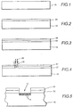
- an electrically insulating substrate 10 is shown in cross-section view. It is desired to form a conductor pattern on the upper surface of this substrate.
- This substrate may be glass, polymer materials or other relatively thermally inefficient materials.
- thermally inefficient we mean that the material is relatively slow to dissipate localized heat. In this sense, this substrate is distinct from such substrates as alumina and the high thermal conductivity metals such as copper which dissipate heat much more rapidly.
- the dividing line between thermally efficient and thermally inefficient materials is in part dependent on the energy of the laser beam used to pattern the metal.
- a first, layer of a thermally inefficient metal 22 is formed on the upper surface of the substrate 10 to provide the structure shown in Figure 2.
- This metal is preferably titanium, but may instead be chrome, nichrome, nickel, stainless steel, magnesium, manganese and so forth.
- This metal is deposited on the substrate under vacuum or other non-oxidizing conditions by any appropriate method, such as sputtering, thermal evaporation, chemical vapor deposition and so forth. We prefer to deposit this metal layer by sputtering. This layer is preferably from 500 to 1,000 ⁇ thick.
- a layer 24 of a UV absorbing metal which is preferably copper but may also be gold, is deposited on top of the layer 22 without breaking the vacuum in the deposition system to provide the structure illustrated in Figure 3.
- This copper layer may preferably be deposited to a depth in the range from 500-3,000 ⁇ . While thicker layers can be used where higher laser power is available, this thickness is adequate to the purpose, and effective with a laser power of 1-2 watts at 351-363 nm. Other wave lengths may be used with other metals having different absorption spectra.
- the substrate with its metal coating is mounted in a laser delivery system which is capable of scanning an intense UV light beam across the substrate.
- This oxidizing atmosphere may be air, air with additional oxygen added to it, pure oxygen, a chlorine containing atmosphere and so forth. We prefer to use air or air plus oxygen.
- the titanium and copper burn as they ablate with a sparkling effect similar to that of Fourth of July sparklers. This sparkling extends substantially above the surface of the metal 24.
- a beneficial side effect of this process where the substrate 10 is a polymer is that the portion of the polymer surface from which the metal is ablated becomes roughened with a surface characteristic which looks much like needles standing on their end.
- This roughened surface is a substantial advantage in a high density interconnect structure or other structure where a subsequent dielectric layer is later formed over the metal pattern and the exposed portions of the substrate 10.
- this is an adhesion promoting technique which can be applied to a polymer surface even where none of the deposited metal is to be retained on the polymer and its only function is to enable the roughening of the polymer surface during its ablation. This results in a greatly increased surface area.
- chrome used as the first or lower metal layer produces a similar sparkling and improvement in pattern definition.
- chrome used as the first or lower metal layer produces a similar sparkling and improvement in pattern definition.
- nickel, stainless steel, magnesium, manganese and similar metals which are or contain highly reactive elements will produce similar sparkling and improvement in pattern definition.
- the process described above must include the provision of the thermally inefficient layer between the substrate and the ultraviolet absorbing metal in order to enable the laser ablation process to remove the UV absorbing metal.
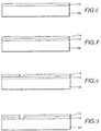
- a layer 112 of a thermally inefficient metal is vacuum deposited on a thermally conducting substrate 100 to provide the structure illustrated in Figure 6.
- This thermally inefficient metal may be titanium, chromium, stainless steel (as a laminated layer) nichrome, magnesium, manganese or other metals or mixtures or alloys of metals which are thermally inefficient and sufficiently reactive.
- the layer 112 is made thick enough to render its upper surface thermally inefficient. That is, the poor thermal efficiency of the layer 112 insulates an overlying layer from the thermal efficiency of the substrate 100.
- a layer 114 of UV absorbing metal is vacuum deposited on the thermally inefficient metal 112 without breaking the vacuum in the deposition apparatus to provide the structure shown in Figure 7.
- the upper metal layer 114 protects the lower metal layer 112 from oxidation and other chemical reactions.
- the metal 114 is then ablated by a laser beam 126 as illustrated in Figure 8. This removes the UV absorbing metal 114 in the laser scan pattern and may also remove part of but not all of the thermally inefficient metal 112.
- At least the lower portion of the thermally inefficient metal remains on the substrate because for a sufficiently thin layer of the thermally inefficient metal, the underlying substrate 100 carries heat away so rapidly that the thermally inefficient layer can not be heated to an ablation temperature.
- the retained portions of that upper metal layer may be used as a mask for chemically etching of the now exposed portions of the thermally inefficient metal 112 to leave portions 120 of the substrate surface metal-free. After such etching of the exposed portions of layer 112, the structure appears as shown in Figure 9.
- a four layer metal structure may be formed prior to laser ablation by successively depositing titanium, copper, titanium and copper to provide a structure of the general type shown in Figure 10.
- These layers may be -1000 ⁇ thick titanium, ⁇ 3000 ⁇ of deposited copper on which copper is electroplated to ⁇ 3mm thick, ⁇ 500-1000 ⁇ thick titanium and ⁇ 500-3000 ⁇ thick copper, respectively.
- the two layers adjacent the substrate technically form part of the substrate as far as the initial ablation is concerned.
- the upper-most copper layer 118 may then be ablated from the upper surface of the upper titanium layer 116 to leave the copper in the desired pattern for the metallization as shown in Figure 11.
- This ablation is generally non-reactive in that no burning or sparkling occurs and none of the titanium appears to be removed during the ablation where the titanium layer is ⁇ 500-1000 ⁇ thick. However, excellent patterning is obtained. This is believed to be in part a result of the impervious nature of the titanium layer.
- the now exposed portions of the underlying titanium may then be etched with an HF-based etchant to expose the thick copper layer 114 as shown in Figure 12. This etchant needs to be one which etches titanium without etching copper.
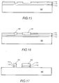
- a copper etch then removes the exposed portions of the lower, thick copper layer 114 and the remaining portions of the upper, thin copper layer 118 to provide the structure shown in Figure 13.
- a final titanium etch removes the now exposed portions of the lower titanium layer 112 and the portions of the upper titanium layer 116 which protected the copper of the conductor runs during the etching of the thick copper layer 114. This results in the structure shown in Figure 14.
- copper layer 114 may be left with a thickness of ⁇ 6000 ⁇ or so and the layers 116 and 118 deposited thereon.
- the process then follows that described above through the etching of the upper titanium layer 116.
- the retained portions of the upper copper layer 118 are removed from the surface of the titanium by a quick copper etch in ferric chloride which leaves the layer 114 of copper ⁇ 3000 ⁇ thick as shown in Figure 15.
- Titanium forms titanium oxide when exposed to air.
- the surface of the upper titanium layer 116 is coated with titanium oxide.
- the resulting titanium oxide layer is sufficiently electrically insulating to prevent electroplating on the titanium, that is, the titanium oxide coated titanium acts as a resist for electroplating.
- this structure may then be electroplated in a copper, gold, chrome or nickel electroplating bath to produce plated conductors having the pattern of the exposed copper 114 without depositing the copper gold, chrome or nickel 122 on the titanium portion of the structure as shown in Figure 16.
- This provides an effective method of forming gold, chrome or nickel plating on copper without the problems of photoresist lifting which have been experienced in the prior art.
- the surface titanium layer may be removed in a HF-based etchant, the portions of the lower copper layer 114 which are not protected by plated metal 122 may be removed in a ferric chloride etchant and the then unprotected portions of the lower titanium layer may be removed in a HF-based etchant.
- the substrate 200 may be a single layer of insulating material or may be a multilayer printed circuit structure (including high density interconnect structures) having an insulating upper surface on which the two portions 210 and 212 of an open trace are disposed with an unintended gap 214 therebetween.
- a first layer 222 of a thermally inefficient, reactive metal such as titanium is deposited over the entire upper surface of the substrate 200 and any conductors thereon.
- a second layer 224 of a UV absorbing metal such as copper is uniformly deposited over the upper surface.
- the entire upper surface of the substrate 200 is conductive.
- the deposited metals are then laser reactive ablated from those portions of the upper surface of the substrate 200 where conductors are not desired, but without ablating the portions of the deposited metals which bridge the gap 214 between the conductors 210 and 212.
- the retained portion of the deposited metals in the vicinity of the gap between the conductors 210 and 212 serve as a bridging conductor to close the gap, thereby repairing the structure as shown in Figure 20.
- This same technique can also be used to provide temporary connections for programming during testing or for other purposes. Such temporary connections can then be removed by etching or by further laser ablation.
- a resistor 310 is disposed on a substrate 300.
- a two layer metallization 320 is disposed on top of the resistor material as its contacts. These contacts can be initially patterned by photomasking and etching. These contacts are then laser ablated to increase the length of the current path through the resistor material between the two contacts to thereby increase the resistance exhibited by the resistor. Alternatively, all of the patterning of these contacts can be done by laser ablation.
Description
- The present invention relates to the fields of metal patterning and electronics, and more particularly, to the patterning of thin layers of metal.
- In the electronic arts, a common method of providing a circuit pattern is to form a layer of metal on an electrically insulating substrate, deposit a layer of photoresist over the the metal, pattern the photoresist photolithographically and etch the metal where it is not protected by the photoresist in order to leave the metal present in the pattern of the retained photoresist. This etching technique is limited in its inability to maintain very fine line lithography due to photoresist lift-off or deterioration, undercutting and other phenomena during etching.
- An alternative technique is to electroplate metal on the portions of the initial metal layer which are not covered by the photoresist. Such a plating process is normally completed by removing the remaining photoresist and etching away the initial metal layer with an etchant which does not attack the electroplated metal. The use of this plating technique to form gold, chrome or nickel electroplated conductors is normally ineffective because the electroplating bath attacks the photoresist vigorously causing deterioration and lift-off of the photoresist which results in plating in areas intended to be kept plating-free.
- A high density interconnect (HDI) structure or system which has been developed by General Electric Company requires patterning of metal conductors disposed on dielectric layers in order to form the interconnections among the integrated circuit chips of a system it is being used to interconnect. This high density interconnect structure offers many advantages in the compact assembly of electronic systems. For example, an electronic system such as a micro computer which incorporates 30-50 chips can be fully assembled and interconnected on a single substrate which is 2 inches long by 2 inches wide by .050 inch thick.
- Briefly, in this high density interconnect structure, a ceramic substrate such as alumina which may be 100 mils thick and of appropriate size and strength for the overall system, is provided. This size is typically less than 2 inches square, but.may be made larger or smaller. Once the position of the various chips has been specified, individual cavities or one large cavity having appropriate depth at the intended locations of differing chips, is prepared. This may be done by starting with a bare substrate having a uniform thickness and the desired size. Conventional, ultrasonic or laser milling may be used to form the cavities in which the various chips and other components will be positioned. For many systems where it is desired to place chips nearly edge-to-edge, a single large cavity is satisfactory. That large cavity may typically have a uniform depth where the semiconductor chips have a substantially uniform thickness. Where a particularly thick or a particularly thin component will be placed, the cavity bottom may be made respectively deeper or shallower to place the upper surface of the corresponding component in substantially the same plane as the upper surface of the rest of the components and the portion of the substrate which surrounds the cavity. The bottom of the cavity is then provided with a thermoplastic adhesive layer which may preferably be polyetherimide resin available under the trade name ULTEM® 6000 from the General Electric Company. The various components are then placed in their desired locations within the cavity, the entire structure is heated to about 300°C which is above the softening point of the ULTEM® polyetherimide (which is in the vicinity of 235°C) and then cooled to thermoplastically bond the individual components to the substrate. Thereafter, a polyimide film which may be Kapton® polyimide, available from E.I. du Pont de Nemours Company, which is =0.0005-0.003 inch (≈12.5-75 microns) thick is pretreated to promote adhesion by reactive ion etching (RIE). The substrate and chips are then coated with ULTEM® 1000 polyetherimide resin or another thermoplastic and the Kapton film is laminated across the top of the chips, any other components and the substrate with the ULTEM® resin serving as a thermoplastic adhesive to hold the Kapton® in place. Thereafter, via holes are provided (preferably by laser drilling) in the Kapton® and ULTEM® layers in alignment with the contact pads on the electronic components to which it is desired to make contact. A metallization layer which is deposited over the Kapton® layer extends into the via holes and makes electrical contact to the contact pads disposed thereunder. This metallization layer may be patterned to form individual conductors during the process of depositing it or may be deposited as a continuous layer and then patterned using photoresist and etching. The photoresist is preferably exposed using a laser to provide an accurately aligned conductor pattern at the end of the process. Additional dielectric and metallization layers are provided as required in order to provide all of the desired electrical connections among the chips.
- Good adhesion of the metal conductors to the underlying dielectric and good adhesion of each dielectric layer to both the underlying metal and the underlying dielectric is necessary for proper fabrication of these high density interconnect circuits.
- This high density interconnect structure, methods of fabricating it and tools for fabricating it are disclosed in U.S. Patent 4,783,695, entitled "Multichip Integrated Circuit Packaging Configuration and Method" by C.W. Eichelberger, et al.; U.S. Patent 4,835,704, entitled "Adaptive Lithography System to Provide High Density Interconnect" by C.W. Eichelberger, et al.; U.S. Patent 4,714,516, entitled "Method to Produce Via Holes in Polymer Dielectrics for Multiple Electronic Circuit Chip Packaging" by C.W. Eichelberger, et al.; U.S. Patent 4,780,177, entitled "Excimer Laser Patterning of a Novel Resist" by R.J. Wojnarowski et al.; U.S. Patent Application Serial No. 249,927, filed September 27, 1989, entitled "Method and Apparatus for Removing Components Bonded to a Substrate" by R.J. Wojnarowski, et al.; U.S. Patent Application Serial No. 310,149, filed February 14, 1989, entitled "Laser Beam Scanning Method for Forming Via Holes in Polymer Materials" by C.W. Eichelberger, et al.; U.S. Patent Application Serial No. 312,798, filed February 21, 1989, entitled "High Density Interconnect Thermoplastic Die Attach Material and Solvent Die Attachment Processing" by R.J. Wojnarowski, et al.; U.S. Patent Application Serial No. 283,095, filed December 12, 1988, entitled "Simplified Method for Repair of High Density Interconnect Circuits" by C.W. Eichelberger, et al.; U.S. Patent Application Serial No. 305,314, filed February 3, 1989, entitled "Fabrication Process and Integrated Circuit Test Structure" by H.S. Cole, et al.; U.S. Patent Application Serial No. 250,010, filed September 27, 1988, entitled "High Density Interconnect With High Volumetric Efficiency" by C.W. Eichelberger, et al.; U.S. Patent Application Serial No. 329,478, filed March 28, 1989, entitled "Die Attachment Method for Use in High Density Interconnected Assemblies" by R.J. Wojnarowski, et al.; U.S. Patent Application Serial No. 253,020,filed October 4, 1988, entitled "Laser Interconnect Process" by H.S. Cole, et al.; U.S. Patent Application Serial No. 230,654, filed August 5, 1988, entitled "Method and Configuration for Testing Electronic Circuits and Integrated Circuit Chips Using a Removable Overlay Layer" by C.W. Eichelberger, et al.; U.S. Patent Application Serial No. 233,965, filed August 8, 1988, entitled "Direct Deposition of Metal Patterns for Use in Integrated Circuit Devices" by Y.S. Liu, et al.; U.S. Patent Application Serial No. 237,638, filed August 23, 1988, entitled "Method for Photopatterning Metallization Via UV Laser Ablation of the Activator" by Y.S. Liu, et al.; U.S. Patent Application Serial No. 237,685, filed August 25, 1988, entitled "Direct Writing of Refractory Metal Lines for Use in Integrated Circuit Devices" by Y.S. Liu, et al.; U.S. Patent Application Serial No. 240,367, filed August 30, 1988, entitled "Method and Apparatus for Packaging Integrated Circuit Chips Employing a Polymer film Overlay Layer" by C.W. Eichelberger, et al.; U.S. Patent Application Serial No. 342,153, filed April 24, 1989, entitled "Method of Processing Siloxane-Polyimides for Electronic Packaging Applications" by H.S. Cole, et al.; U.S. Patent Application Serial No. 289,944, filed December 27, 1988, entitled "Selective Electrolytic Deposition on Conductive and Non-Conductive Substrates" by Y.S. Liu, et al.; U.S. Patent Application Serial No. 312,536, filed February 17, 1989, entitled "Method of Bonding a Thermoset Film to a Thermoplastic Material to Form a Bondable Laminate" by R.J. Wojnarowski; U.S. Patent Application Serial No. 363,646, filed June 8, 1989, entitled "Integrated Circuit Packaging Configuration for Rapid Customized Design and Unique Test Capability" by C.W. Eichelberger, et al.; U.S. Patent Application Serial No. 07/459,844, filed January 2, 1990, entitled "Area-Selective Metallization Process" by H.S. Cole, et al.; U.S. patent application Serial No. 361,623, filed June 5, 1989, entitled, "Adaptive Lithography Accommodation of Tolerances and Chip Positioning in High Density Interconnect Structures", by T.R. Haller; U.S. Patent Application Serial No. 07/457,023, filed December 26, 1989, entitled "Locally Orientation Specific Routing System" by T.R. Haller, et al.; U.S. Patent Application Serial No. 456,421, filed December 26, 1989, entitled "Laser Ablatable Polymer Dielectrics and Methods" by H.S. Cole, et al.; U.S. Patent Application Serial No. 454,546, filed December 21, 1989, entitled "Hermetic High Density Interconnected Electronic System" by W.P. Kornrumpf, et al.; U.S. Patent Application Serial No. 07/457,127, filed December 26, 1989, entitled "Enhanced Fluorescence Polymers and Interconnect Structures Using Them" by H.S. Cole, et al.; U.S. Patent Application Serial No. 454,545, filed December 21, 1989, entitled "An Epoxy/Polyimide Copolymer Blend Dielectric and Layered Circuits Incorporating It" by C.W. Eichelberger, et al.; Application Serial No. 07/504,760, filed April 5, 1990, entitled, "A Building Block Approach to Microwave Modules", by W. P. Kornrumpf et al.; Application Serial No. 07/504,821, filed April 5, 1990, entitled, "HDI Microwave Circuit Assembly", by W. P. Kornrumpf, et al.; Application Serial No. 07/504,750 filed April 5, 1990, entitled, "An Ultrasonic Array With a High Density of Electrical Connections", by L. S. Smith, et al.; Application Serial No. 07/504,803, filed April 5, 1990, entitled, "Microwave Component Test Method and Apparatus", by W. P. Kornrumpf, et al.; Application Serial No. 07/504,753, filed April 5, 1990, entitled, "A Compact High Density Interconnected Microwave System", by W. P. Kornrumpf; Application Serial No. 07/504,769, filed April 5, 1990, entitled, "A Flexible High Density Interconnect Structure and Flexibly Interconnected System" by C. W. Eichelberger, et al.; Application Serial No. 07/504,751, filed April 5, 1990, entitled, "Compact, Thermally Efficient Focal Plane Array and Testing and Repair Thereof", by W. P. Kornrumpf, et al.; Application Serial No. 07/504,749, filed April 5, 1990, entitled, "High Density Interconnect Structure with Top Mounted Components", by R. J. Wojnarowski, et al.; Application Serial No. 07/504,770, filed April 5, 1990, entitled, "A High Density Interconnect Structure Including a Chamber", by R. J. Wojnarowski, et al.; Application Serial No. 07/504,748, filed April 5, 1990, entitled, "Microwave Component Having Tailored Operating Characteristics and Method of Tailoring" by W. P. Kornrumpf, et al.; Application Serial No. 07/546,963, filed July 2, 1990, entitled "Multiple Lamination High Density Interconnect Process and Structure Employing Thermoplastic Adhesives having Sequentially Decreasing Tg's" by H.S. Cole et al.; Application Serial No.07/546,964, filed July 2, 1990, entitled "High Temperature Polyether Imide Compositions and Method of Making" by J.H. Lupinski et al.; Application Serial No.07/545,793, filed June 29,1990, entitled, "Adaptive Lithography in a High Density Interconnect Structure Whose Signal Layers Have Fixed Patterns" by T.R. Haller et al.; Application Serial No. 07/546,965, filed July 2, 1990, entitled "A High Density Interconnect Structure Including a Spacer Structure and a Gap", by H.S. Cole et al.; Application Serial No.07/546,959, filed July 2, 1990, entitled, "Multiple Lamination High Density Interconnect Process and Structure Employing a Variable Crosslinking Adhesive", by T.B.Gorczyca et al.; Application Serial No.07/546,230, filed June 29, 1990, entitled, "Method of Developing a Self-Developing Resist", by H.S. Cole, et al.; Application Serial No.07/546,960, filed July 2, 1990, entitled, "Multi-Sublayer Dielectric Layers, by H.S. Cole et al.; and Application Serial No.07/548,462, filed July 2, 1990, entitled, "Compact High Density Interconnect Structure", by W.M. Marcinkiewicz et al..
- There is a continuing need for improved metal patterning techniques and for enhanced inter-dielectric layer adhesion.
- Accordingly, the present invention seeks to provide an improved metal patterning technique which enables copper, gold, chrome and nickel patterns to be formed with high definition and reliability.
- The present invention also seeks to provide an improved technique for producing high definition conductor patterns by patterned removal of a uniform conducting layer.
- The present invention also seeks to provide a laser ablation technique for patterning conductive layers.
- The present invention also seeks, in one embodiment thereof, to provide a metal patterning technique in which two layers of different metals burn off together during laser patterning.
- The present invention also seeks to provide a laser metal patterning technique which is useful on high thermal conductivity substrates.
- US-A-4,826,785 describes a metallic interconnect including a fuse portion that is readily vaporized upon exposure to the radiant energy of a laser. A layer of optically absorptive material is formed on top of an aluminum based metallic interconnect and together they are formed by a photolithographic and etch technique into a first portion. A low energy laser having a Gaussian energy distribution focused on the absorptive layer produces heat in the absorptive layer. The heat is transferred to the underlying aluminum based interconnect. The concentration of energy made possible by the absorptive layer allows the low energy laser to blow the fuse thereby producing an electrical open in the interconnect without damaging surrounding silicon substrate and/or polysilicon structures below or nearby the metal fuse.
- According to the invention, there is provided a method of producing a desired metal pattern on a surface of a substrate comprising, depositing a layer of a first metal on said substrate, one of said substrate and the resulting surface of said first metal having a low thermal conductivity; depositing a layer of a second, ultraviolet light absorbing metal on said first metal without breaking vacuum; exposing said second metal to intense ultraviolet light in accordance with said desired pattern to ablate at least said second metal.
- In accordance with one embodiment, a first layer of a thermally inefficient, reactive metal is deposited on an electrically insulating substrate and a second ultraviolet light absorbing metal is deposited on that first metal. The resulting structure is scanned with a UV laser having sufficient power to ablate the first and second metals together to remove them from the substrate in a pattern which is determined by the scanning pattern of the laser beam, while leaving them on the substrate elsewhere. Where the substrate is a polymer and the first layer is titanium or chrome and the second layer is copper, the portion of the polymer surface from which the metals were ablated is greatly roughened. If a subsequent dielectric layer is formed on top of this roughened surface by applying a liquid precursor and drying or curing it, then adhesion between the two layers is greatly enhanced by a resulting interlocking of the newly deposited dielectric layer with the roughened surface of the substrate.
- In accordance with another embodiment, where the substrate is highly thermally conducting, an initial layer of a thermally inefficient metal such as titanium, chrome, stainless steel and so forth is disposed on the substrate prior to deposition of a subsequent layer of UV absorbing metal. This layer of thermally inefficient metal is made thick enough to cause the combined structure to act as a thermally inefficient substrate. The UV absorbing metal is then ablated from the surface of the thermally inefficient metal to create a metal pattern with good definition. The remaining portions of the second metal layer may then be used as a mask for etching those portions of the first metal which were exposed by the ablation of the second metal. Thereafter, the second metal may be retained or removed, as may be desired.
- In accordance with another embodiment, a four layer metal structure may be deposited on a thermally conducting substrate with the third layer being thermally inefficient and the fourth layer being UV absorbing the first and second layers, in the present context, being a part of the substrate. The fourth layer is then patterned by scanning a laser across it. That fourth layer is then used as an etching mask for the third, thermally inefficient layer. The second layer and then the first layer may be etched to provide a conductor pattern of the second layer metal over first layer metal. When the third layer is titanium, the remaining portions of the fourth layer may be removed and additional metal may be electroplated on the exposed portions of the second layer without plating on the titanium.
- In accordance with another embodiment, a printed circuit having a break in an intended-to-be-continuous trace is repaired by depositing an thermally inefficient metal over the entire surface, depositing a UV absorbing metal over the first metal and then ablating the two deposited layers every place where conductors are not desired. The result is a bridging conductor which connects the two pieces of the trace across the unintended gap therein.
- The invention will now be described in greater detail, by way of example, with reference to the drawings in which:
- Figures 1-5 illustrate a sequence of stages in the production of a metal pattern in accordance with one embodiment of the invention;
- Figures 6-9 illustrate a sequence of stags in th fabrication of a pattern in accordance with another embodiment;
- Figures 10-14 illustrate stages in another embodiment;
- Figures 15-17 illustrate stages in an electroplating process;
- Figures 18-20 illustrate circuit repair;
- Figure 21 illustrates trimming of a resistor to adjust its resistance.
- In Figure 1, an electrically insulating
substrate 10 is shown in cross-section view. It is desired to form a conductor pattern on the upper surface of this substrate. This substrate may be glass, polymer materials or other relatively thermally inefficient materials. By thermally inefficient, we mean that the material is relatively slow to dissipate localized heat. In this sense, this substrate is distinct from such substrates as alumina and the high thermal conductivity metals such as copper which dissipate heat much more rapidly. The dividing line between thermally efficient and thermally inefficient materials is in part dependent on the energy of the laser beam used to pattern the metal. - As an initial step in the process of forming the conductor pattern, a first, layer of a thermally
inefficient metal 22 is formed on the upper surface of thesubstrate 10 to provide the structure shown in Figure 2. This metal is preferably titanium, but may instead be chrome, nichrome, nickel, stainless steel, magnesium, manganese and so forth. This metal is deposited on the substrate under vacuum or other non-oxidizing conditions by any appropriate method, such as sputtering, thermal evaporation, chemical vapor deposition and so forth. We prefer to deposit this metal layer by sputtering. This layer is preferably from 500 to 1,000Å thick. Subsequently, alayer 24 of a UV absorbing metal which is preferably copper but may also be gold, is deposited on top of thelayer 22 without breaking the vacuum in the deposition system to provide the structure illustrated in Figure 3. This copper layer may preferably be deposited to a depth in the range from 500-3,000Å. While thicker layers can be used where higher laser power is available, this thickness is adequate to the purpose, and effective with a laser power of 1-2 watts at 351-363 nm. Other wave lengths may be used with other metals having different absorption spectra. Next, the substrate with its metal coating is mounted in a laser delivery system which is capable of scanning an intense UV light beam across the substrate. We prefer to use an argon ion laser operating at 351 nm, but other frequencies may also be used. The laser is then scanned across the surface of themetal 24 in a pattern which corresponds to the areas in which metal is to be removed as illustrated in Figure 4. The copper absorbs roughly 60% of the UV light incident thereon and is heated to an ablation temperature. Direct ablation of the titanium itself without an overlying absorbing layer is not effective because titanium reflects about 81% of incident 351 nm light. However, there is sufficient thermal coupling between the copper and the titanium that the laser heating of the copper heats the underlying titanium to an ablation temperature which results in the two metals ablating off the substrate together. We prefer to perform this ablation process in an oxidizing atmosphere. This oxidizing atmosphere may be air, air with additional oxygen added to it, pure oxygen, a chlorine containing atmosphere and so forth. We prefer to use air or air plus oxygen. In this oxidizing atmosphere, the titanium and copper burn as they ablate with a sparkling effect similar to that of Fourth of July sparklers. This sparkling extends substantially above the surface of themetal 24. - With this process, we have obtained line spacings of from 2 to 500 microns, while retaining metal patterns of from 2 to 500 microns wide. Wider or narrower lines and spaces may be produced in accordance with the laser beam size and scanning pattern used for the ablation.
- A beneficial side effect of this process where the
substrate 10 is a polymer is that the portion of the polymer surface from which the metal is ablated becomes roughened with a surface characteristic which looks much like needles standing on their end. This is illustrated in Figure 5 where theportion 12 of thesubstrate surface 10 from which the metal was ablated has needle-like columns 14 extending roughly vertically. In many instances these columns are mushroom shaped with their upper end larger in cross section than their stem or shank. This roughened surface is a substantial advantage in a high density interconnect structure or other structure where a subsequent dielectric layer is later formed over the metal pattern and the exposed portions of thesubstrate 10. If that subsequent layer is formed by spinning on or spraying on a liquid precursor which is then converted to a solid dielectric in situ, greatly enhanced adhesion results from the infiltration of the subsequent dielectric layer into the gaps between theneedles 14 in the roughened surface of the substrate. This provides improved adhesion for a subsequently formed dielectric layer in two ways. First, it provides an increased contact surface area over which chemical adhesion is provided and second, it provides a rough surface which results in mechanical interlocking of the two layers which further increases the strength of the bond between the two layers. This mushroom shape of many of the needles further enhances mechanical interlocking of dielectric layers. As a consequence, use of this process to pattern conductor layers in multilayer structures provides additional benefits in providing a more rugged, more thoroughly bonded structure. Thus, this is an adhesion promoting technique which can be applied to a polymer surface even where none of the deposited metal is to be retained on the polymer and its only function is to enable the roughening of the polymer surface during its ablation. This results in a greatly increased surface area. - The combination of these two metals (copper over titanium) results in much sharper patterning than can be obtained with copper alone even where the substrate on which the copper alone is disposed is a substantially poorer thermal conductor than titanium. It is clear that the two metals interact during ablation in accordance with this invention. We therefore refer to this process as reactive ablation. When copper alone is used, no sparkling results, the line edge definition is much poorer and with a polymer substrate the surface of the polymer remains conductive as a result of some of the copper being left behind. It is believed that the copper which is left behind is actually driven into the surface of the polymer. Thus, use of copper alone results in inferior patterning and inferior surface properties for the resulting structure. As is mentioned above, if titanium alone is used, no ablation takes place at these laser powers because not enough energy is absorbed by the titanium to raise it to an ablation temperature. Thus, the combination of the two metals is necessary for high quality definition of the pattern and that high quality is a result of an unexpected interaction between the two metals during the ablation which results in reactive ablation. This interaction affects the removal of the metals themselves from the substrate, and thus is not a reaction which takes place only in the debris which has already left the surface of the substrate, but also involves the metals while they are still disposed on that surface. Since titanium is highly reactive and in the initial structure has been protected from oxidation by the deposition of the copper layer directly over the titanium without breaking the vacuum in the metal deposition system, it is thought that oxidation is taking place at the exposed edge of the titanium as the laser beam heats the copper which in turn heats the titanium. That oxidation then further heats the titanium resulting in the sparkling effect and the improved definition of the ablation pattern as compared to the pattern when copper alone is present. However, whether this is in fact the actual process is not known at this time. Further, the exact chemical and thermal processes going on is unimportant, since our work establishes that whatever processes are in fact taking place produce the beneficial effects of improved pattern definition, result in a non-conductive surface even on polymer substrates and on polymer substrates produce the needles-on-end surface pattern which greatly increases the exposed surface area of the polymer where the metals have been ablated.
- In addition to titanium, chrome used as the first or lower metal layer produces a similar sparkling and improvement in pattern definition. Nichrome, nickel, stainless steel, magnesium, manganese and similar metals which are or contain highly reactive elements will produce similar sparkling and improvement in pattern definition.
- In accordance with another embodiment of the invention where it is desired to form a metal pattern on a highly thermally conducting substrate such as alumina or a high thermal conductivity metal, the process described above must include the provision of the thermally inefficient layer between the substrate and the ultraviolet absorbing metal in order to enable the laser ablation process to remove the UV absorbing metal. To this end, a
layer 112 of a thermally inefficient metal is vacuum deposited on a thermally conductingsubstrate 100 to provide the structure illustrated in Figure 6. This thermally inefficient metal may be titanium, chromium, stainless steel (as a laminated layer) nichrome, magnesium, manganese or other metals or mixtures or alloys of metals which are thermally inefficient and sufficiently reactive. Thelayer 112 is made thick enough to render its upper surface thermally inefficient. That is, the poor thermal efficiency of thelayer 112 insulates an overlying layer from the thermal efficiency of thesubstrate 100. Thereafter, alayer 114 of UV absorbing metal is vacuum deposited on the thermallyinefficient metal 112 without breaking the vacuum in the deposition apparatus to provide the structure shown in Figure 7. Theupper metal layer 114 protects thelower metal layer 112 from oxidation and other chemical reactions. Themetal 114 is then ablated by alaser beam 126 as illustrated in Figure 8. This removes theUV absorbing metal 114 in the laser scan pattern and may also remove part of but not all of the thermallyinefficient metal 112. At least the lower portion of the thermally inefficient metal remains on the substrate because for a sufficiently thin layer of the thermally inefficient metal, theunderlying substrate 100 carries heat away so rapidly that the thermally inefficient layer can not be heated to an ablation temperature. After the ablative patterning of the UV absorbingmetal layer 114, the retained portions of that upper metal layer may be used as a mask for chemically etching of the now exposed portions of the thermallyinefficient metal 112 to leave portions 120 of the substrate surface metal-free. After such etching of the exposed portions oflayer 112, the structure appears as shown in Figure 9. - As an alternative to employing the just described two layer metal structure, a four layer metal structure may be formed prior to laser ablation by successively depositing titanium, copper, titanium and copper to provide a structure of the general type shown in Figure 10. These layers may be -1000Å thick titanium, ∼3000Å of deposited copper on which copper is electroplated to ∼3mm thick, ∼500-1000Å thick titanium and ∼500-3000Å thick copper, respectively. In this embodiment the two layers adjacent the substrate technically form part of the substrate as far as the initial ablation is concerned. The
upper-most copper layer 118 may then be ablated from the upper surface of theupper titanium layer 116 to leave the copper in the desired pattern for the metallization as shown in Figure 11. This ablation is generally non-reactive in that no burning or sparkling occurs and none of the titanium appears to be removed during the ablation where the titanium layer is ∼500-1000Å thick. However, excellent patterning is obtained. This is believed to be in part a result of the impervious nature of the titanium layer. The now exposed portions of the underlying titanium may then be etched with an HF-based etchant to expose thethick copper layer 114 as shown in Figure 12. This etchant needs to be one which etches titanium without etching copper. A copper etch then removes the exposed portions of the lower,thick copper layer 114 and the remaining portions of the upper,thin copper layer 118 to provide the structure shown in Figure 13. A final titanium etch removes the now exposed portions of thelower titanium layer 112 and the portions of theupper titanium layer 116 which protected the copper of the conductor runs during the etching of thethick copper layer 114. This results in the structure shown in Figure 14. - Alternatively, rather than electroplating the
first copper layer 114 to thicken it, thatcopper layer 114 may be left with a thickness of ∼6000Å or so and thelayers upper titanium layer 116. Then the retained portions of theupper copper layer 118 are removed from the surface of the titanium by a quick copper etch in ferric chloride which leaves thelayer 114 of copper ∼3000Å thick as shown in Figure 15. Titanium forms titanium oxide when exposed to air. As a result, the surface of theupper titanium layer 116 is coated with titanium oxide. The resulting titanium oxide layer is sufficiently electrically insulating to prevent electroplating on the titanium, that is, the titanium oxide coated titanium acts as a resist for electroplating. Thus, this structure may then be electroplated in a copper, gold, chrome or nickel electroplating bath to produce plated conductors having the pattern of the exposedcopper 114 without depositing the copper gold, chrome ornickel 122 on the titanium portion of the structure as shown in Figure 16. This provides an effective method of forming gold, chrome or nickel plating on copper without the problems of photoresist lifting which have been experienced in the prior art. Following this plating operation, the surface titanium layer may be removed in a HF-based etchant, the portions of thelower copper layer 114 which are not protected by platedmetal 122 may be removed in a ferric chloride etchant and the then unprotected portions of the lower titanium layer may be removed in a HF-based etchant. The result is the structure illustrated in Figure 17 in which electroplated copper, gold, chrome or nickel conductors are provided. While this process is highly effective for copper electroplating, its benefits are more pronounced for gold, chromium and nickel electroplating because copper plating baths attack photoresist much more slowly than gold, chromium and nickel electroplating baths do with the result that prior electroplating of copper has been much more successful than prior art electroplating of gold, chromium and nickel. - This metal deposition and ablation technique is also suitable for repairing open conductors in printed circuit type structures such as printed circuit boards, VLSI integrated circuits, wafer scale integrated structures, high density interconnect structures and so forth. Such a printed circuit is shown in perspective view in Figure 18. The
substrate 200 may be a single layer of insulating material or may be a multilayer printed circuit structure (including high density interconnect structures) having an insulating upper surface on which the twoportions unintended gap 214 therebetween. Where thegap 214 between theconductors conductors - To effect a repair of this open trace, a
first layer 222 of a thermally inefficient, reactive metal such as titanium is deposited over the entire upper surface of thesubstrate 200 and any conductors thereon. Subsequently, asecond layer 224 of a UV absorbing metal such as copper is uniformly deposited over the upper surface. At this stage, as shown in Figure 19, the entire upper surface of thesubstrate 200 is conductive. The deposited metals are then laser reactive ablated from those portions of the upper surface of thesubstrate 200 where conductors are not desired, but without ablating the portions of the deposited metals which bridge thegap 214 between theconductors conductors - This same technique can also be used to provide temporary connections for programming during testing or for other purposes. Such temporary connections can then be removed by etching or by further laser ablation.
- This technique is also useful for trimming resistors. In Figure 21, a
resistor 310 is disposed on asubstrate 300. A twolayer metallization 320 is disposed on top of the resistor material as its contacts. These contacts can be initially patterned by photomasking and etching. These contacts are then laser ablated to increase the length of the current path through the resistor material between the two contacts to thereby increase the resistance exhibited by the resistor. Alternatively, all of the patterning of these contacts can be done by laser ablation. - While the invention has been described in detail herein in accord with certain preferred embodiments thereof, many modifications and changes therein may be effected by those skilled in the art. Accordingly, it is intended by the appended claims to cover all such modifications and changes as fall within the scope of the invention which is as defined by the claims.
Claims (11)
- A method of producing a desired metal pattern on a surface of a substrate comprising :depositing a layer of a first metal on said substrate, one of said substrate and the resulting surface of said first metal having a low thermal conductivity;depositing a layer of a second, ultraviolet light absorbing metal on said first metal without breaking vacuum;exposing said second metal to intense ultraviolet light in accordance with said desired pattern to ablate at least said second metal.
- The method of Claim 1 wherein said substrate has a low thermal conductivity and said exposing step includes reactively ablating said first and second metals together.
- The method of Claim 1 wherein said first metal layer is thick enough to render the resulting surface of low thermal conductivity.
- The method recited in Claim 1, 2 or 3, wherein:said first metal is selected from the group consisting of titanium, chromium, magnesium, manganese, nichrome and stainless steel and alloys and mixtures thereof; andsaid second metal is selected from the group consisting of copper and gold and alloys and mixtures thereof.
- The method recited in Claims 1-4 wherein said substrate is disposed in an oxidizing atmosphere during said exposing step.
- The method recited in Claim 5, wherein said first and second metals burn off the substrate together during said exposing step.
- The method recited in Claim 5 wherein said oxidizing atmosphere comprises air.
- The method recited in Claim 5 wherein said oxidizing atmosphere comprises oxygen.
- The method recited in any one of Claims 1 to 8, wherein the step of exposing comprises scanning an ultraviolet laser beam across said substrate.
- The method recited in Claim 3 or any claim appendant directly or indirectly thereto further comprising etching exposed portions of said first metal with an etchant which does not attack said second metal.
- The method recited in Claim 3 or any claim appendant directly or indirectly thereto, wherein said substrate is electrically conducting, said first metal is titanium and said method further comprises, after the step of exposing, the step of:selectively removing said second metal from said titanium;allowing the titanium thus exposed to form a surface coating of titanium oxide; andelectroplating said substrate to build up electroplated metal in those areas from which said metals were ablated without building up electroplated metal on said titanium.
Applications Claiming Priority (2)
| Application Number | Priority Date | Filing Date | Title |
|---|---|---|---|
| US07/597,255 US5104480A (en) | 1990-10-12 | 1990-10-12 | Direct patterning of metals over a thermally inefficient surface using a laser |
| US597255 | 1990-10-12 |
Publications (3)
| Publication Number | Publication Date |
|---|---|
| EP0480703A2 EP0480703A2 (en) | 1992-04-15 |
| EP0480703A3 EP0480703A3 (en) | 1992-06-03 |
| EP0480703B1 true EP0480703B1 (en) | 1997-03-26 |
Family
ID=24390748
Family Applications (1)
| Application Number | Title | Priority Date | Filing Date |
|---|---|---|---|
| EP91309278A Expired - Lifetime EP0480703B1 (en) | 1990-10-12 | 1991-10-09 | Producing metal patterns on a substrate |
Country Status (4)
| Country | Link |
|---|---|
| US (1) | US5104480A (en) |
| EP (1) | EP0480703B1 (en) |
| JP (1) | JP3338465B2 (en) |
| DE (1) | DE69125333T2 (en) |
Cited By (4)
| Publication number | Priority date | Publication date | Assignee | Title |
|---|---|---|---|---|
| US6911621B2 (en) | 2000-11-01 | 2005-06-28 | Roche Diagnostics Corporation | Biosensor |
| US7073246B2 (en) | 1999-10-04 | 2006-07-11 | Roche Diagnostics Operations, Inc. | Method of making a biosensor |
| US7287318B2 (en) | 2000-10-06 | 2007-10-30 | Roche Diagnostics Operations, Inc. | Biosensor |
| US8551308B2 (en) | 1999-10-04 | 2013-10-08 | Roche Diagnostics Operations, Inc. | Biosensor and method of making |
Families Citing this family (61)
| Publication number | Priority date | Publication date | Assignee | Title |
|---|---|---|---|---|
| GB9221099D0 (en) * | 1992-10-07 | 1992-11-18 | Ecossensors Ltd | Improvements in and relating to gas permeable membranes for amperometric gas electrodes |
| JP3400067B2 (en) * | 1994-03-16 | 2003-04-28 | 富士通株式会社 | Method and apparatus for cutting conductor of printed wiring board |
| US6518088B1 (en) | 1994-09-23 | 2003-02-11 | Siemens N.V. And Interuniversitair Micro-Electronica Centrum Vzw | Polymer stud grid array |
| DE59508519D1 (en) * | 1994-09-23 | 2000-08-03 | Siemens Nv | Polymer stud grid array package |
| US5505320A (en) * | 1994-11-22 | 1996-04-09 | International Business Machines Corporation | Method employing laser ablating for providing a pattern on a substrate |
| US5567329A (en) * | 1995-01-27 | 1996-10-22 | Martin Marietta Corporation | Method and system for fabricating a multilayer laminate for a printed wiring board, and a printed wiring board formed thereby |
| US5821505A (en) * | 1997-04-04 | 1998-10-13 | Unisys Corporation | Temperature control system for an electronic device which achieves a quick response by interposing a heater between the device and a heat sink |
| EP0877417A1 (en) * | 1997-05-09 | 1998-11-11 | Lucent Technologies Inc. | Method for fabrication of electrodes and other electrically-conductive structures |
| US6141870A (en) | 1997-08-04 | 2000-11-07 | Peter K. Trzyna | Method for making electrical device |
| US6350555B1 (en) | 1998-01-14 | 2002-02-26 | Precision Coatings, Inc. | Direct write imaging medium |
| US6261941B1 (en) * | 1998-02-12 | 2001-07-17 | Georgia Tech Research Corp. | Method for manufacturing a multilayer wiring substrate |
| DE19913367C1 (en) * | 1999-03-24 | 2000-12-14 | Siemens Ag | Method of making an electrical circuit |
| US6462629B1 (en) | 1999-06-15 | 2002-10-08 | Cts Corporation | Ablative RF ceramic block filters |
| FR2795907B1 (en) * | 1999-07-01 | 2007-02-16 | Gemplus Card Int | PROCESS FOR THE MANUFACTURE AND TESTING OF ELECTRONIC MICROMODULAS, IN PARTICULAR FOR CHIP CARDS |
| US6662439B1 (en) | 1999-10-04 | 2003-12-16 | Roche Diagnostics Corporation | Laser defined features for patterned laminates and electrodes |
| US6388230B1 (en) * | 1999-10-13 | 2002-05-14 | Morton International, Inc. | Laser imaging of thin layer electronic circuitry material |
| US6559735B1 (en) | 2000-10-31 | 2003-05-06 | Cts Corporation | Duplexer filter with an alternative signal path |
| CN1229763C (en) * | 2000-11-14 | 2005-11-30 | 东陶机器株式会社 | Sign forming method and article obtained thereby |
| CA2434969A1 (en) * | 2001-02-01 | 2002-08-08 | Electro Scientific Industries, Inc. | Resistor trimming with small uniform spot from solid-state uv laser |
| US6534743B2 (en) * | 2001-02-01 | 2003-03-18 | Electro Scientific Industries, Inc. | Resistor trimming with small uniform spot from solid-state UV laser |
| US6571468B1 (en) | 2001-02-26 | 2003-06-03 | Saturn Electronics & Engineering, Inc. | Traceless flip chip assembly and method |
| DE10112023A1 (en) * | 2001-03-07 | 2002-10-02 | Atotech Deutschland Gmbh | Method of forming a metal pattern on a dielectric substrate |
| US6528869B1 (en) | 2001-04-06 | 2003-03-04 | Amkor Technology, Inc. | Semiconductor package with molded substrate and recessed input/output terminals |
| US20020170897A1 (en) * | 2001-05-21 | 2002-11-21 | Hall Frank L. | Methods for preparing ball grid array substrates via use of a laser |
| US6586826B1 (en) | 2001-06-13 | 2003-07-01 | Amkor Technology, Inc. | Integrated circuit package having posts for connection to other packages and substrates |
| US6814844B2 (en) | 2001-08-29 | 2004-11-09 | Roche Diagnostics Corporation | Biosensor with code pattern |
| US20040173894A1 (en) * | 2001-09-27 | 2004-09-09 | Amkor Technology, Inc. | Integrated circuit package including interconnection posts for multiple electrical connections |
| JP4155031B2 (en) * | 2002-03-15 | 2008-09-24 | 株式会社豊田中央研究所 | Substrate surface modification method, modified substrate, and apparatus |
| US6866758B2 (en) * | 2002-03-21 | 2005-03-15 | Roche Diagnostics Corporation | Biosensor |
| US6951995B2 (en) * | 2002-03-27 | 2005-10-04 | Gsi Lumonics Corp. | Method and system for high-speed, precise micromachining an array of devices |
| US7563695B2 (en) * | 2002-03-27 | 2009-07-21 | Gsi Group Corporation | Method and system for high-speed precise laser trimming and scan lens for use therein |
| US6822332B2 (en) * | 2002-09-23 | 2004-11-23 | International Business Machines Corporation | Fine line circuitization |
| GB0224121D0 (en) * | 2002-10-16 | 2002-11-27 | Microemissive Displays Ltd | Method of patterning a functional material on to a substrate |
| US20040091588A1 (en) * | 2002-10-31 | 2004-05-13 | Xiaochun Li | Food processing apparatus and method |
| CN1846131B (en) | 2003-06-20 | 2012-01-18 | 霍夫曼-拉罗奇有限公司 | Method and reagent for producing narrow, homogenous reagent strips |
| KR100784497B1 (en) * | 2004-10-06 | 2007-12-11 | 삼성전자주식회사 | Film substrate of semiconductor package and manufacturing method thereof |
| WO2006100202A1 (en) * | 2005-03-23 | 2006-09-28 | Technische Universität Ilmenau | Method for laser microstructuring a material using a protective layer with a threshold intensity defined by reflection and absorption characteristics |
| JP4639975B2 (en) * | 2005-06-07 | 2011-02-23 | パナソニック電工株式会社 | Manufacturing method of three-dimensional circuit board |
| DE102005030272A1 (en) * | 2005-06-21 | 2007-01-04 | Hansgrohe Ag | Method for producing decorative surface structures |
| KR20070004373A (en) * | 2005-07-04 | 2007-01-09 | 삼성전자주식회사 | Built-in type antenna pattern for mobile phone and method for manufacturing the same |
| US8290239B2 (en) * | 2005-10-21 | 2012-10-16 | Orbotech Ltd. | Automatic repair of electric circuits |
| US7510985B1 (en) | 2005-10-26 | 2009-03-31 | Lpkf Laser & Electronics Ag | Method to manufacture high-precision RFID straps and RFID antennas using a laser |
| US20070138153A1 (en) * | 2005-12-20 | 2007-06-21 | Redman Dean E | Wide web laser ablation |
| US8647654B2 (en) * | 2005-12-22 | 2014-02-11 | The Penn State Research Foundation | Method and systems for forming and using nanoengineered sculptured thin films |
| US20070215575A1 (en) * | 2006-03-15 | 2007-09-20 | Bo Gu | Method and system for high-speed, precise, laser-based modification of one or more electrical elements |
| JP4706690B2 (en) * | 2007-11-05 | 2011-06-22 | パナソニック電工株式会社 | Circuit board and manufacturing method thereof |
| WO2009149152A1 (en) * | 2008-06-03 | 2009-12-10 | The Government Of The United States Of America, As Represented By The Secretary Of The Navy | Surface enhanced raman detection on metallized nanostructured polymer films |
| JP5405916B2 (en) * | 2008-06-24 | 2014-02-05 | パナソニック株式会社 | Biosensor, method for manufacturing the same, and detection system including the same |
| US20100294352A1 (en) * | 2009-05-20 | 2010-11-25 | Uma Srinivasan | Metal patterning for electrically conductive structures based on alloy formation |
| JP2011233872A (en) * | 2010-04-08 | 2011-11-17 | Asahi Glass Co Ltd | Method for manufacturing substrate with metal pattern, and substrate with metal laminate |
| US8593727B2 (en) | 2011-04-25 | 2013-11-26 | Vladimir G. Kozlov | Single-shot laser ablation of a metal film on a polymer membrane |
| RU2494492C1 (en) * | 2012-06-07 | 2013-09-27 | Общество с ограниченной ответственностью "Компания РМТ" | Method to create conducting paths |
| US10537027B2 (en) | 2013-08-02 | 2020-01-14 | Orbotech Ltd. | Method producing a conductive path on a substrate |
| EP2887418A1 (en) * | 2013-12-19 | 2015-06-24 | The Swatch Group Research and Development Ltd. | Cell with non-conducting structured surface |
| ES2901943T3 (en) * | 2014-04-16 | 2022-03-24 | Abbott Lab | Droplet actuator manufacturing apparatus, systems and related methods |
| US10087527B2 (en) * | 2014-04-30 | 2018-10-02 | Wistron Neweb Corp. | Method of fabricating substrate structure and substrate structure fabricated by the same method |
| US9842740B2 (en) | 2014-08-29 | 2017-12-12 | Seagate Technology Llc | Ablation for feature recovery |
| US10369565B2 (en) | 2014-12-31 | 2019-08-06 | Abbott Laboratories | Digital microfluidic dilution apparatus, systems, and related methods |
| KR101810815B1 (en) * | 2017-04-07 | 2017-12-20 | 김병삼 | Manufacturing method of sensor cover penetrating electronic signal having micro crack and laser hole |
| DE102018115205A1 (en) | 2018-06-25 | 2020-01-02 | Vishay Electronic Gmbh | Process for manufacturing a large number of resistance units |
| CN111343793A (en) * | 2020-03-12 | 2020-06-26 | 电子科技大学 | Surface metallization method for printed circuit composite dielectric substrate |
Family Cites Families (7)
| Publication number | Priority date | Publication date | Assignee | Title |
|---|---|---|---|---|
| US3867217A (en) * | 1973-10-29 | 1975-02-18 | Bell Telephone Labor Inc | Methods for making electronic circuits |
| DE2521543A1 (en) * | 1974-05-16 | 1975-11-27 | Crosfield Electronics Ltd | METHOD AND DEVICE FOR REPRODUCING IMAGES |
| US4259433A (en) * | 1976-10-22 | 1981-03-31 | Fuji Photo Film Co., Ltd. | Method for producing disk-recording plates |
| US4713518A (en) * | 1984-06-08 | 1987-12-15 | Semiconductor Energy Laboratory Co., Ltd. | Electronic device manufacturing methods |
| JPS61108195A (en) * | 1984-11-01 | 1986-05-26 | インタ−ナショナル ビジネス マシ−ンズ コ−ポレ−ション | Formation of electrically continued layers on substrate |
| US4786358A (en) * | 1986-08-08 | 1988-11-22 | Semiconductor Energy Laboratory Co., Ltd. | Method for forming a pattern of a film on a substrate with a laser beam |
| US4826785A (en) * | 1987-01-27 | 1989-05-02 | Inmos Corporation | Metallic fuse with optically absorptive layer |
-
1990
- 1990-10-12 US US07/597,255 patent/US5104480A/en not_active Expired - Lifetime
-
1991
- 1991-10-03 JP JP28202991A patent/JP3338465B2/en not_active Expired - Fee Related
- 1991-10-09 EP EP91309278A patent/EP0480703B1/en not_active Expired - Lifetime
- 1991-10-09 DE DE69125333T patent/DE69125333T2/en not_active Expired - Fee Related
Cited By (4)
| Publication number | Priority date | Publication date | Assignee | Title |
|---|---|---|---|---|
| US7073246B2 (en) | 1999-10-04 | 2006-07-11 | Roche Diagnostics Operations, Inc. | Method of making a biosensor |
| US8551308B2 (en) | 1999-10-04 | 2013-10-08 | Roche Diagnostics Operations, Inc. | Biosensor and method of making |
| US7287318B2 (en) | 2000-10-06 | 2007-10-30 | Roche Diagnostics Operations, Inc. | Biosensor |
| US6911621B2 (en) | 2000-11-01 | 2005-06-28 | Roche Diagnostics Corporation | Biosensor |
Also Published As
| Publication number | Publication date |
|---|---|
| US5104480A (en) | 1992-04-14 |
| JP3338465B2 (en) | 2002-10-28 |
| EP0480703A2 (en) | 1992-04-15 |
| DE69125333D1 (en) | 1997-04-30 |
| DE69125333T2 (en) | 1997-10-02 |
| EP0480703A3 (en) | 1992-06-03 |
| JPH04280494A (en) | 1992-10-06 |
Similar Documents
| Publication | Publication Date | Title |
|---|---|---|
| EP0480703B1 (en) | Producing metal patterns on a substrate | |
| JP3587884B2 (en) | Method for manufacturing multilayer circuit board | |
| US5302547A (en) | Systems for patterning dielectrics by laser ablation | |
| US4764485A (en) | Method for producing via holes in polymer dielectrics | |
| US5236551A (en) | Rework of polymeric dielectric electrical interconnect by laser photoablation | |
| US6119335A (en) | Method for manufacturing multi-layer printed circuit board | |
| US4880959A (en) | Process for interconnecting thin-film electrical circuits | |
| US5107586A (en) | Method for interconnecting a stack of integrated circuits at a very high density | |
| EP0074605B1 (en) | Method for manufacturing multilayer circuit substrate | |
| US4983250A (en) | Method of laser patterning an electrical interconnect | |
| US4704304A (en) | Method for repair of opens in thin film lines on a substrate | |
| EP0450381B1 (en) | Multilayer interconnection structure | |
| US5127998A (en) | Area-selective metallization process | |
| JPH10214920A (en) | Improved type polytetrafluoroethylene thin film chip carrier | |
| US20010001214A1 (en) | Technique for producing interconnecting conductive links | |
| US5230965A (en) | High density interconnect with electroplated conductors | |
| JPH07202424A (en) | Production of multilayer wiring board | |
| US5550325A (en) | Printed-circuit board including circuit pattern having location to be cut if necessary | |
| JP3154964B2 (en) | Printed circuit board and its laser drilling method | |
| JP3136682B2 (en) | Method for manufacturing multilayer wiring board | |
| JPH07283544A (en) | Wiring structure and its manufacturing method | |
| JP3265289B2 (en) | Manufacturing method of aluminum nitride substrate | |
| GB2307351A (en) | Printed circuit boards and their manufacture | |
| Kersten et al. | Excimer laser structuring of epoxy resin layers for MCM‐L Applications | |
| JPH1117330A (en) | Manufacture of multilayered wiring board, and the multilayered wiring board |
Legal Events
| Date | Code | Title | Description |
|---|---|---|---|
| PUAI | Public reference made under article 153(3) epc to a published international application that has entered the european phase |
Free format text: ORIGINAL CODE: 0009012 |
|
| AK | Designated contracting states |
Kind code of ref document: A2 Designated state(s): DE FR GB IT |
|
| PUAL | Search report despatched |
Free format text: ORIGINAL CODE: 0009013 |
|
| AK | Designated contracting states |
Kind code of ref document: A3 Designated state(s): DE FR GB IT |
|
| 17P | Request for examination filed |
Effective date: 19921123 |
|
| 17Q | First examination report despatched |
Effective date: 19941005 |
|
| GRAG | Despatch of communication of intention to grant |
Free format text: ORIGINAL CODE: EPIDOS AGRA |
|
| GRAH | Despatch of communication of intention to grant a patent |
Free format text: ORIGINAL CODE: EPIDOS IGRA |
|
| GRAH | Despatch of communication of intention to grant a patent |
Free format text: ORIGINAL CODE: EPIDOS IGRA |
|
| GRAA | (expected) grant |
Free format text: ORIGINAL CODE: 0009210 |
|
| AK | Designated contracting states |
Kind code of ref document: B1 Designated state(s): DE FR GB IT |
|
| ET | Fr: translation filed | ||
| REF | Corresponds to: |
Ref document number: 69125333 Country of ref document: DE Date of ref document: 19970430 |
|
| PLBE | No opposition filed within time limit |
Free format text: ORIGINAL CODE: 0009261 |
|
| STAA | Information on the status of an ep patent application or granted ep patent |
Free format text: STATUS: NO OPPOSITION FILED WITHIN TIME LIMIT |
|
| 26N | No opposition filed | ||
| REG | Reference to a national code |
Ref country code: FR Ref legal event code: TP |
|
| PGFP | Annual fee paid to national office [announced via postgrant information from national office to epo] |
Ref country code: FR Payment date: 20010920 Year of fee payment: 11 Ref country code: DE Payment date: 20010920 Year of fee payment: 11 |
|
| PGFP | Annual fee paid to national office [announced via postgrant information from national office to epo] |
Ref country code: GB Payment date: 20010921 Year of fee payment: 11 |
|
| REG | Reference to a national code |
Ref country code: GB Ref legal event code: 732E |
|
| REG | Reference to a national code |
Ref country code: GB Ref legal event code: IF02 |
|
| PG25 | Lapsed in a contracting state [announced via postgrant information from national office to epo] |
Ref country code: GB Free format text: LAPSE BECAUSE OF NON-PAYMENT OF DUE FEES Effective date: 20021009 |
|
| PG25 | Lapsed in a contracting state [announced via postgrant information from national office to epo] |
Ref country code: DE Free format text: LAPSE BECAUSE OF NON-PAYMENT OF DUE FEES Effective date: 20030501 |
|
| GBPC | Gb: european patent ceased through non-payment of renewal fee |
Effective date: 20021009 |
|
| PG25 | Lapsed in a contracting state [announced via postgrant information from national office to epo] |
Ref country code: FR Free format text: LAPSE BECAUSE OF NON-PAYMENT OF DUE FEES Effective date: 20030630 |
|
| REG | Reference to a national code |
Ref country code: FR Ref legal event code: ST |
|
| PG25 | Lapsed in a contracting state [announced via postgrant information from national office to epo] |
Ref country code: IT Free format text: LAPSE BECAUSE OF NON-PAYMENT OF DUE FEES Effective date: 20051009 |