EP0485216A2 - Liquid-crystal colour display - Google Patents
Liquid-crystal colour display Download PDFInfo
- Publication number
- EP0485216A2 EP0485216A2 EP91310319A EP91310319A EP0485216A2 EP 0485216 A2 EP0485216 A2 EP 0485216A2 EP 91310319 A EP91310319 A EP 91310319A EP 91310319 A EP91310319 A EP 91310319A EP 0485216 A2 EP0485216 A2 EP 0485216A2
- Authority
- EP
- European Patent Office
- Prior art keywords
- display
- liquid crystal
- light
- color
- crystal layer
- Prior art date
- Legal status (The legal status is an assumption and is not a legal conclusion. Google has not performed a legal analysis and makes no representation as to the accuracy of the status listed.)
- Granted
Links
Images


Classifications
-
- G—PHYSICS
- G02—OPTICS
- G02F—OPTICAL DEVICES OR ARRANGEMENTS FOR THE CONTROL OF LIGHT BY MODIFICATION OF THE OPTICAL PROPERTIES OF THE MEDIA OF THE ELEMENTS INVOLVED THEREIN; NON-LINEAR OPTICS; FREQUENCY-CHANGING OF LIGHT; OPTICAL LOGIC ELEMENTS; OPTICAL ANALOGUE/DIGITAL CONVERTERS
- G02F1/00—Devices or arrangements for the control of the intensity, colour, phase, polarisation or direction of light arriving from an independent light source, e.g. switching, gating or modulating; Non-linear optics
- G02F1/01—Devices or arrangements for the control of the intensity, colour, phase, polarisation or direction of light arriving from an independent light source, e.g. switching, gating or modulating; Non-linear optics for the control of the intensity, phase, polarisation or colour
- G02F1/13—Devices or arrangements for the control of the intensity, colour, phase, polarisation or direction of light arriving from an independent light source, e.g. switching, gating or modulating; Non-linear optics for the control of the intensity, phase, polarisation or colour based on liquid crystals, e.g. single liquid crystal display cells
- G02F1/133—Constructional arrangements; Operation of liquid crystal cells; Circuit arrangements
- G02F1/1333—Constructional arrangements; Manufacturing methods
- G02F1/1343—Electrodes
- G02F1/134309—Electrodes characterised by their geometrical arrangement
- G02F1/134327—Segmented, e.g. alpha numeric display
-
- G—PHYSICS
- G02—OPTICS
- G02F—OPTICAL DEVICES OR ARRANGEMENTS FOR THE CONTROL OF LIGHT BY MODIFICATION OF THE OPTICAL PROPERTIES OF THE MEDIA OF THE ELEMENTS INVOLVED THEREIN; NON-LINEAR OPTICS; FREQUENCY-CHANGING OF LIGHT; OPTICAL LOGIC ELEMENTS; OPTICAL ANALOGUE/DIGITAL CONVERTERS
- G02F1/00—Devices or arrangements for the control of the intensity, colour, phase, polarisation or direction of light arriving from an independent light source, e.g. switching, gating or modulating; Non-linear optics
- G02F1/01—Devices or arrangements for the control of the intensity, colour, phase, polarisation or direction of light arriving from an independent light source, e.g. switching, gating or modulating; Non-linear optics for the control of the intensity, phase, polarisation or colour
- G02F1/13—Devices or arrangements for the control of the intensity, colour, phase, polarisation or direction of light arriving from an independent light source, e.g. switching, gating or modulating; Non-linear optics for the control of the intensity, phase, polarisation or colour based on liquid crystals, e.g. single liquid crystal display cells
- G02F1/133—Constructional arrangements; Operation of liquid crystal cells; Circuit arrangements
- G02F1/1333—Constructional arrangements; Manufacturing methods
- G02F1/1335—Structural association of cells with optical devices, e.g. polarisers or reflectors
- G02F1/133509—Filters, e.g. light shielding masks
- G02F1/133514—Colour filters
Definitions
- the present invention relates to a liquid-crystal color display.
- a liquid-crystal color display in which, as shown in Fig.4, display patterns are formed by portions where transparent comb electrodes 21 and 22 on the SEG (segment) side, serving as pixel electrodes, overlap transparent electrodes 23 and 24 on the COM (common) side, respectively.
- Each element of the SEG-side pixel electrode 21 faces a red color filter not shown, while each element of SEG-side pixel electrode 22 faces a green color filter not shown.
- the display patterns are independent individually and are connected to different signal lines.
- the display area C where display patterns are defined by the SEG-side pixel electrode 21 is separated from the display area D where display patterns are defined by the SEG-side pixel electrode 22, and the display areas C and D cannot be brought in contact with each other or made to overlap. It is therefore not possible to make a plurality of display patterns overlap each other within one display area, the resulting problem being an inability to further increase the number of display patterns per unit display area.
- the present invention provides a liquid-crystal color display comprising: a plurality of color selecting members provided for transmitting light of specific colors respectively and formed over one entire surface of one of a pair of light-transmitting substrates disposed opposite each other sandwiching a liquid crystal layer between them, the one entire surface being on the side facing the liquid crystal layer; a light blocking member interposed between the adjacent color selecting members; and light-transmitting pixel electrodes which are respectively provided in the display areas on the sides facing the liquid crystal layer of the pair of light-transmitting substrates and which, in response to electrical signals, alter the molecular alignment in the liquid crystal layer in the portion thereof facing the specific color selecting member selected in accordance with the color to be displayed in the display area, the liquid-crystal color display being characterized in that the pixel electrodes disposed adjacent to each other correspond to different color selecting members and are formed in such a manner as to extend into each other's display area in alternating fashion.
- the pixel electrodes disposed adjacent to each other are formed extending into each other's display area, display patterns formed by the adjacent pixel electrodes can be made to overlap each other within one display area. Therefore, according to the invention, the number of display patterns per unit display area can be increased.
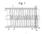
- Fig.1 is a detail drawing of an essential portion of a liquid-crystal color display in one embodiment of the invention.
- transparent comb electrodes 1 and 2 formed on the SEG-side and serving as pixel electrodes, are disposed facing a red color filter R and a green color filter G, respectively.
- the reference sign B indicates a blue color filter.
- Two light-transmitting substrates, one on the SEG side and the other on the COM side, are disposed opposite each other sandwiching a liquid crystal layer (not shown) between them.
- the color filters, red R, green G, and blue B are disposed over one entire surface of the SEG-side light-transmitting substrate, the entire surface being on the side facing the liquid crystal layer.
- the SEG-side transparent comb electrodes 1 and 2 are formed on the liquid crystal layer side of the SEG-side light-transmitting substrate.
- the SEG-side transparent comb electrodes 1 and 2 are arranged extending into each other's area in alternating fashion.
- the SEG-side transparent electrodes 1 and 2 share a COM-side electrode 3 disposed opposite them across the liquid crystal layer not shown and form two different display patterns, upper and lower, respectively driven independently of each other.
- a mask 6 which serves as a light blocking member formed extending between the color filters R, G, B.
- production of the above display patterns is achieved by applying varying voltages to the SEG-side transparent comb electrodes 1, 2 and the COM-side electrode 3 and thereby varying the molecular alignment in the liquid crystal layer.
- overlapping portions 5 are formed where the display area defined by the SEG-side transparent electrode 1 overlaps the display area defined by the SEG-side transparent electrode 2. That is, in the liquid-crystal color display of this embodiment, since the display area A, where the red display pattern defined by the SEG-side transparent electrode 1 is formed, overlaps the display area B where the green display area defined by the SEG-side transparent electrode 2 is formed, the number of display patterns per unit display area can be increased.
Abstract
Description
- The present invention relates to a liquid-crystal color display.
- It is known to provide a liquid-crystal color display in which, as shown in Fig.4, display patterns are formed by portions where
transparent comb electrodes transparent electrodes side pixel electrode 21 faces a red color filter not shown, while each element of SEG-side pixel electrode 22 faces a green color filter not shown. The display patterns are independent individually and are connected to different signal lines. - In the above prior art liquid-crystal color display, however, as shown in Fig.5, the display area C where display patterns are defined by the SEG-
side pixel electrode 21 is separated from the display area D where display patterns are defined by the SEG-side pixel electrode 22, and the display areas C and D cannot be brought in contact with each other or made to overlap. It is therefore not possible to make a plurality of display patterns overlap each other within one display area, the resulting problem being an inability to further increase the number of display patterns per unit display area. - It is accordingly an object of the invention to provide a liquid-crystal color display which permits a plurality of display patterns to overlap each other within one display area and thereby achieves an increase in the number of display patterns per unit display area.
- To achieve the above object, the present invention provides a liquid-crystal color display comprising: a plurality of color selecting members provided for transmitting light of specific colors respectively and formed over one entire surface of one of a pair of light-transmitting substrates disposed opposite each other sandwiching a liquid crystal layer between them, the one entire surface being on the side facing the liquid crystal layer; a light blocking member interposed between the adjacent color selecting members; and light-transmitting pixel electrodes which are respectively provided in the display areas on the sides facing the liquid crystal layer of the pair of light-transmitting substrates and which, in response to electrical signals, alter the molecular alignment in the liquid crystal layer in the portion thereof facing the specific color selecting member selected in accordance with the color to be displayed in the display area, the liquid-crystal color display being characterized in that the pixel electrodes disposed adjacent to each other correspond to different color selecting members and are formed in such a manner as to extend into each other's display area in alternating fashion.
- According to the above construction, since the pixel electrodes disposed adjacent to each other are formed extending into each other's display area in alternating fashion, display patterns formed by the adjacent pixel electrodes are made to overlap each other within one display area, which serves to increase the number of display patterns per unit display area.
- As is apparent from the above description, in the liquid-crystal color display of the invention, since the pixel electrodes disposed adjacent to each other are formed extending into each other's display area, display patterns formed by the adjacent pixel electrodes can be made to overlap each other within one display area. Therefore, according to the invention, the number of display patterns per unit display area can be increased.
- Other and further objects, features, and advantages of the invention will be more explicit from the following detailed description taken with reference to the drawings wherein:
- Fig.1 is a detail drawing of an essential portion of a liquid-crystal color display in one embodiment of the invention;
- Fig.2 is a diagram showing how display areas overlap each other in the above embodiment;
- Fig.3 is a plan view showing color filters and a mask in accordance with the above embodiment;
- Fig.4 is a detail drawing of an essential portion of a prior art liquid-crystal color display; and
- Fig.5 is a drawing showing display areas in the prior art liquid-crystal color display.
- Now referring to the drawing, preferred embodiments of the invention are described below.
- Fig.1 is a detail drawing of an essential portion of a liquid-crystal color display in one embodiment of the invention. In this embodiment,
transparent comb electrodes transparent comb electrodes transparent comb electrodes transparent electrodes side electrode 3 disposed opposite them across the liquid crystal layer not shown and form two different display patterns, upper and lower, respectively driven independently of each other. In Fig.3 is shown a mask 6 which serves as a light blocking member formed extending between the color filters R, G, B. - In this embodiment, production of the above display patterns is achieved by applying varying voltages to the SEG-side
transparent comb electrodes side electrode 3 and thereby varying the molecular alignment in the liquid crystal layer. Also, in this embodiment, overlapping portions 5 are formed where the display area defined by the SEG-sidetransparent electrode 1 overlaps the display area defined by the SEG-sidetransparent electrode 2. That is, in the liquid-crystal color display of this embodiment, since the display area A, where the red display pattern defined by the SEG-sidetransparent electrode 1 is formed, overlaps the display area B where the green display area defined by the SEG-sidetransparent electrode 2 is formed, the number of display patterns per unit display area can be increased. - The invention may be embodied in other specific forms without departing from the spirit or essential characteristics thereof. The present embodiments are therefore to be considered in all respects as illustrative and not restrictive, the scope of the invention being indicated by the appended claims rather than by the foregoing description and all changes which come within the meaning and the range of equivalency of the claims are therefore intended to be embraced therein.
- There are described above novel features which the skilled man will appreciate give rise to advantages. These are each independent aspects of the invention to be covered by the application, irrespective of whether or not they are included within the scope of the following claims.
Claims (5)
- A liquid crystal color display comprising:
a plurality of color selecting members (R,G,B) provided for transmitting light of specific colors respectively and formed over one entire surface of one of a pair of light-transmitting substrates disposed opposite each other sandwiching a liquid crystal layer between them, the one entire surface being on the side facing the liquid crystal layer;
a light blocking member (6) interposed between the adjacent color selecting members (R,G,B); and
light-transmitting pixel electrodes which are respectively provided in the display areas on the sides facing the liquid crystal layer of the pair of light-transmitting substrates and which, in response to electrical signals, alter the molecular alignment in the liquid crystal layer in the portion thereof facing the specific color selecting member (R,G,B) selected in accordance with the color to be displayed in the display area,
the liquid-crystal color display being characterized in that the pixel electrodes disposed adjacent to each other correspond to different color selecting members (R,G,B) and are formed in such a manner as to extend into each other's display area in alternating fashion. - A liquid-crystal color display as set forth in Claim 1, wherein: the pair of light-transmitting substrates disposed opposite each other with the liquid crystal layer sandwiched between them are provided with SEG-side (1,2) and COM-side (3) transparent electrodes respectively, the color selecting members (R,G,B) and the light blocking member (6) being provided on the substrate on which the SEG-side transparent electrodes (1,2) are formed.
- A liquid-crystal color di-splay as set forth in Claim 1, wherein: the color selecting members are color filters of three colors, red (R), green (G), and blue (B).
- A colour liquid crystal display device divided into first and second adjacent display areas for displaying in different respective colours, comprising a liquid crystal layer, first and second colour selection members for allowing display in the different respective colours in the respective display areas, first and second display electrodes for selectively allowing transmission of light through the liquid crystal layer in respective ones of the first and second display areas in accordance with electrical signals, characterised in that end portions of the first and second display electrodes are adjacent in a direction along the boundary between the first and second display areas thereby allowing the display areas to overlap.
- A colour liquid crystal display according to claim 4 wherein the first and second colour selection members each comprise a plurality of strip-like filters extending across both the first and second adjacent display areas.
Applications Claiming Priority (2)
| Application Number | Priority Date | Filing Date | Title |
|---|---|---|---|
| JP303077/90 | 1990-11-07 | ||
| JP2303077A JPH04174417A (en) | 1990-11-07 | 1990-11-07 | Color liquid crystal display device |
Publications (3)
| Publication Number | Publication Date |
|---|---|
| EP0485216A2 true EP0485216A2 (en) | 1992-05-13 |
| EP0485216A3 EP0485216A3 (en) | 1992-10-07 |
| EP0485216B1 EP0485216B1 (en) | 1996-02-07 |
Family
ID=17916620
Family Applications (1)
| Application Number | Title | Priority Date | Filing Date |
|---|---|---|---|
| EP91310319A Expired - Lifetime EP0485216B1 (en) | 1990-11-07 | 1991-11-07 | Liquid-crystal colour display |
Country Status (4)
| Country | Link |
|---|---|
| US (1) | US5233449A (en) |
| EP (1) | EP0485216B1 (en) |
| JP (1) | JPH04174417A (en) |
| DE (1) | DE69116983T2 (en) |
Families Citing this family (16)
| Publication number | Priority date | Publication date | Assignee | Title |
|---|---|---|---|---|
| TW386169B (en) * | 1993-07-27 | 2000-04-01 | Tokyo Shibaura Electric Co | Liquid crystal display apparatus |
| FR2712109B1 (en) * | 1993-11-04 | 1995-12-15 | Ebauchesfabrik Eta Ag | Liquid crystal display device. |
| KR100304912B1 (en) * | 1993-12-30 | 2002-08-24 | 엘지.필립스 엘시디 주식회사 | Structure and Driving Method of LCD |
| JPH10325961A (en) * | 1994-03-17 | 1998-12-08 | Hitachi Ltd | Active matrix type liquid crystal display device |
| US5420052A (en) * | 1994-04-19 | 1995-05-30 | Texas Instruments Incorporated | Method of fabricating a semiplanar heterojunction bipolar transistor |
| JP3529460B2 (en) * | 1994-12-01 | 2004-05-24 | 株式会社東芝 | Liquid crystal display |
| TW329500B (en) | 1995-11-14 | 1998-04-11 | Handotai Energy Kenkyusho Kk | Electro-optical device |
| JPH09146108A (en) * | 1995-11-17 | 1997-06-06 | Semiconductor Energy Lab Co Ltd | Liquid crystal display device and its driving method |
| JP2776376B2 (en) * | 1996-06-21 | 1998-07-16 | 日本電気株式会社 | Active matrix liquid crystal display panel |
| KR100250796B1 (en) * | 1996-11-29 | 2000-04-01 | 김영환 | Liquid crystal display element and its manufacturing method |
| JPH10186366A (en) * | 1996-12-26 | 1998-07-14 | Fujitsu Ltd | Liquid crystal display device |
| US6704083B1 (en) * | 1997-05-30 | 2004-03-09 | Samsung Electronics, Co., Ltd. | Liquid crystal display including polarizing plate having polarizing directions neither parallel nor perpendicular to average alignment direction of molecules |
| TW434443B (en) | 1997-05-30 | 2001-05-16 | Samsung Electronics Co Ltd | Liquid crystal display |
| KR100293806B1 (en) * | 1997-06-25 | 2001-10-24 | 박종섭 | Liquid crystal display |
| GB2327797A (en) * | 1997-07-31 | 1999-02-03 | Sharp Kk | Spatial light modulator and display |
| JP2014206639A (en) * | 2013-04-12 | 2014-10-30 | 株式会社ジャパンディスプレイ | Liquid crystal display device |
Citations (4)
| Publication number | Priority date | Publication date | Assignee | Title |
|---|---|---|---|---|
| EP0219064A2 (en) * | 1985-10-09 | 1987-04-22 | Hitachi, Ltd. | Color liquid crystal display device |
| JPS6370828A (en) * | 1986-09-12 | 1988-03-31 | Matsushita Electric Ind Co Ltd | Matrix type liquid crystal display device and its production |
| EP0317850A2 (en) * | 1987-11-24 | 1989-05-31 | Hitachi, Ltd. | Liquid crystal display device |
| US4902103A (en) * | 1987-08-10 | 1990-02-20 | Koito Manufacturing Co., Ltd. | Color liquid-crystal display unit with electrodes interleaved in vertical and horizontal directions |
Family Cites Families (6)
| Publication number | Priority date | Publication date | Assignee | Title |
|---|---|---|---|---|
| US3820875A (en) * | 1972-04-14 | 1974-06-28 | W Bohmer | Scanner devices utilizing field effect light scattering dielectrics |
| JPS55134885A (en) * | 1979-04-06 | 1980-10-21 | Stanley Electric Co Ltd | Liquid crystal display device |
| JPS59136718A (en) * | 1983-01-26 | 1984-08-06 | Mitsubishi Electric Corp | Liquid crystal display element |
| JPH0748259B2 (en) * | 1987-06-24 | 1995-05-24 | 松下電器産業株式会社 | Optical disc recording / reproducing device |
| JPS6436120A (en) * | 1987-07-30 | 1989-02-07 | Nec Corp | Redundant constitution gate array |
| EP0434220B1 (en) * | 1989-11-20 | 1996-04-10 | Sharp Kabushiki Kaisha | Colour liquid crystal display device |
-
1990
- 1990-11-07 JP JP2303077A patent/JPH04174417A/en active Pending
-
1991
- 1991-11-04 US US07/787,020 patent/US5233449A/en not_active Expired - Lifetime
- 1991-11-07 EP EP91310319A patent/EP0485216B1/en not_active Expired - Lifetime
- 1991-11-07 DE DE69116983T patent/DE69116983T2/en not_active Expired - Fee Related
Patent Citations (4)
| Publication number | Priority date | Publication date | Assignee | Title |
|---|---|---|---|---|
| EP0219064A2 (en) * | 1985-10-09 | 1987-04-22 | Hitachi, Ltd. | Color liquid crystal display device |
| JPS6370828A (en) * | 1986-09-12 | 1988-03-31 | Matsushita Electric Ind Co Ltd | Matrix type liquid crystal display device and its production |
| US4902103A (en) * | 1987-08-10 | 1990-02-20 | Koito Manufacturing Co., Ltd. | Color liquid-crystal display unit with electrodes interleaved in vertical and horizontal directions |
| EP0317850A2 (en) * | 1987-11-24 | 1989-05-31 | Hitachi, Ltd. | Liquid crystal display device |
Non-Patent Citations (1)
| Title |
|---|
| PATENT ABSTRACTS OF JAPAN vol. 12, no. 298 (P-744)(3145) 15 August 1988 & JP-A-63 070 828 ( MATSUSHITA ) * |
Also Published As
| Publication number | Publication date |
|---|---|
| US5233449A (en) | 1993-08-03 |
| DE69116983T2 (en) | 1996-07-18 |
| EP0485216B1 (en) | 1996-02-07 |
| EP0485216A3 (en) | 1992-10-07 |
| JPH04174417A (en) | 1992-06-22 |
| DE69116983D1 (en) | 1996-03-21 |
Similar Documents
| Publication | Publication Date | Title |
|---|---|---|
| EP0485216A2 (en) | Liquid-crystal colour display | |
| US4902103A (en) | Color liquid-crystal display unit with electrodes interleaved in vertical and horizontal directions | |
| EP0302653B1 (en) | Colour display | |
| US6118584A (en) | Autostereoscopic display apparatus | |
| US20020167480A1 (en) | Electrophoretic color display device | |
| KR100186818B1 (en) | Color filter substrate and liquid crystal display device | |
| US5530570A (en) | Color liquid crystal display arrangement with elongated color filters | |
| KR970016724A (en) | Liquid crystal display device having overlapping color filter | |
| CN108398826A (en) | special-shaped display panel and display device | |
| EP0219064B1 (en) | Color liquid crystal display device | |
| EP0476797B1 (en) | Liquid crystal display device | |
| CN109683386A (en) | Built-in touch-control liquid crystal display | |
| EP0317850A2 (en) | Liquid crystal display device | |
| US5223962A (en) | Liquid-crystal color display with parallelogram-shaped pixels | |
| JPS6169091A (en) | Matrix type liquid crystal color display | |
| JPS6283721A (en) | Color liquid crystal display element | |
| JPH07104283A (en) | Color liquid crystal display device | |
| JP2000352721A (en) | Liquid crystal display device | |
| JPH0561035A (en) | Liquid crystal display device | |
| JPS6259924A (en) | Matrix type liquid crystal display device | |
| KR940009165B1 (en) | Multi-color lcd | |
| JPH0643779Y2 (en) | Liquid crystal display element | |
| JPH03223716A (en) | Color liquid crystal display device | |
| JPH01319093A (en) | Liquid crystal display device | |
| JPH0644119B2 (en) | Liquid crystal display element |
Legal Events
| Date | Code | Title | Description |
|---|---|---|---|
| PUAI | Public reference made under article 153(3) epc to a published international application that has entered the european phase |
Free format text: ORIGINAL CODE: 0009012 |
|
| AK | Designated contracting states |
Kind code of ref document: A2 Designated state(s): DE FR GB |
|
| PUAL | Search report despatched |
Free format text: ORIGINAL CODE: 0009013 |
|
| AK | Designated contracting states |
Kind code of ref document: A3 Designated state(s): DE FR GB |
|
| 17P | Request for examination filed |
Effective date: 19921215 |
|
| 17Q | First examination report despatched |
Effective date: 19940531 |
|
| GRAA | (expected) grant |
Free format text: ORIGINAL CODE: 0009210 |
|
| AK | Designated contracting states |
Kind code of ref document: B1 Designated state(s): DE FR GB |
|
| REF | Corresponds to: |
Ref document number: 69116983 Country of ref document: DE Date of ref document: 19960321 |
|
| ET | Fr: translation filed | ||
| PLBE | No opposition filed within time limit |
Free format text: ORIGINAL CODE: 0009261 |
|
| STAA | Information on the status of an ep patent application or granted ep patent |
Free format text: STATUS: NO OPPOSITION FILED WITHIN TIME LIMIT |
|
| 26N | No opposition filed | ||
| PGFP | Annual fee paid to national office [announced via postgrant information from national office to epo] |
Ref country code: GB Payment date: 20011107 Year of fee payment: 11 |
|
| PGFP | Annual fee paid to national office [announced via postgrant information from national office to epo] |
Ref country code: FR Payment date: 20011113 Year of fee payment: 11 |
|
| PGFP | Annual fee paid to national office [announced via postgrant information from national office to epo] |
Ref country code: DE Payment date: 20011119 Year of fee payment: 11 |
|
| REG | Reference to a national code |
Ref country code: GB Ref legal event code: IF02 |
|
| PG25 | Lapsed in a contracting state [announced via postgrant information from national office to epo] |
Ref country code: GB Free format text: LAPSE BECAUSE OF NON-PAYMENT OF DUE FEES Effective date: 20021107 |
|
| PG25 | Lapsed in a contracting state [announced via postgrant information from national office to epo] |
Ref country code: DE Free format text: LAPSE BECAUSE OF NON-PAYMENT OF DUE FEES Effective date: 20030603 |
|
| GBPC | Gb: european patent ceased through non-payment of renewal fee | ||
| PG25 | Lapsed in a contracting state [announced via postgrant information from national office to epo] |
Ref country code: FR Free format text: LAPSE BECAUSE OF NON-PAYMENT OF DUE FEES Effective date: 20030731 |
|
| REG | Reference to a national code |
Ref country code: FR Ref legal event code: ST |