EP0487220A2 - SOI-Field effect transistor and method of manufacturing the same - Google Patents
SOI-Field effect transistor and method of manufacturing the same Download PDFInfo
- Publication number
- EP0487220A2 EP0487220A2 EP91310089A EP91310089A EP0487220A2 EP 0487220 A2 EP0487220 A2 EP 0487220A2 EP 91310089 A EP91310089 A EP 91310089A EP 91310089 A EP91310089 A EP 91310089A EP 0487220 A2 EP0487220 A2 EP 0487220A2
- Authority
- EP
- European Patent Office
- Prior art keywords
- drain regions
- semiconductor layer
- gate electrode
- source
- semiconductor device
- Prior art date
- Legal status (The legal status is an assumption and is not a legal conclusion. Google has not performed a legal analysis and makes no representation as to the accuracy of the status listed.)
- Granted
Links
- 238000004519 manufacturing process Methods 0.000 title claims description 29
- 230000000694 effects Effects 0.000 title description 8
- 239000004065 semiconductor Substances 0.000 claims abstract description 75
- XUIMIQQOPSSXEZ-UHFFFAOYSA-N Silicon Chemical compound [Si] XUIMIQQOPSSXEZ-UHFFFAOYSA-N 0.000 claims abstract description 59
- 229910052710 silicon Inorganic materials 0.000 claims abstract description 59
- 239000010703 silicon Substances 0.000 claims abstract description 59
- 239000012535 impurity Substances 0.000 claims abstract description 48
- 239000012212 insulator Substances 0.000 claims abstract description 22
- 238000005468 ion implantation Methods 0.000 claims abstract description 21
- 239000000758 substrate Substances 0.000 claims description 16
- 229910052698 phosphorus Inorganic materials 0.000 claims description 11
- 239000011574 phosphorus Substances 0.000 claims description 11
- -1 oxygen ions Chemical class 0.000 claims description 9
- OAICVXFJPJFONN-UHFFFAOYSA-N Phosphorus Chemical compound [P] OAICVXFJPJFONN-UHFFFAOYSA-N 0.000 claims description 7
- 238000010438 heat treatment Methods 0.000 claims description 7
- VYPSYNLAJGMNEJ-UHFFFAOYSA-N Silicium dioxide Chemical compound O=[Si]=O VYPSYNLAJGMNEJ-UHFFFAOYSA-N 0.000 claims description 5
- 229910052785 arsenic Inorganic materials 0.000 claims description 5
- 229910052814 silicon oxide Inorganic materials 0.000 claims description 5
- ZOXJGFHDIHLPTG-UHFFFAOYSA-N Boron Chemical compound [B] ZOXJGFHDIHLPTG-UHFFFAOYSA-N 0.000 claims description 4
- 229910052796 boron Inorganic materials 0.000 claims description 4
- 229910052760 oxygen Inorganic materials 0.000 claims description 4
- 239000001301 oxygen Substances 0.000 claims description 4
- RQNWIZPPADIBDY-UHFFFAOYSA-N arsenic atom Chemical compound [As] RQNWIZPPADIBDY-UHFFFAOYSA-N 0.000 claims description 3
- 239000012299 nitrogen atmosphere Substances 0.000 claims description 2
- 238000009792 diffusion process Methods 0.000 abstract description 7
- 230000005669 field effect Effects 0.000 abstract description 2
- 239000010410 layer Substances 0.000 description 68
- 108091006146 Channels Proteins 0.000 description 30
- 239000010409 thin film Substances 0.000 description 24
- 239000010408 film Substances 0.000 description 18
- 238000000034 method Methods 0.000 description 17
- 230000008569 process Effects 0.000 description 15
- 230000005684 electric field Effects 0.000 description 6
- 239000011229 interlayer Substances 0.000 description 5
- 150000002500 ions Chemical class 0.000 description 5
- 229910021420 polycrystalline silicon Inorganic materials 0.000 description 5
- 238000002513 implantation Methods 0.000 description 4
- 230000015572 biosynthetic process Effects 0.000 description 3
- 238000005229 chemical vapour deposition Methods 0.000 description 3
- 230000009467 reduction Effects 0.000 description 3
- 229910052782 aluminium Inorganic materials 0.000 description 2
- XAGFODPZIPBFFR-UHFFFAOYSA-N aluminium Chemical compound [Al] XAGFODPZIPBFFR-UHFFFAOYSA-N 0.000 description 2
- 230000004888 barrier function Effects 0.000 description 2
- 239000000969 carrier Substances 0.000 description 2
- 239000007772 electrode material Substances 0.000 description 2
- 230000001678 irradiating effect Effects 0.000 description 2
- 230000003647 oxidation Effects 0.000 description 2
- 238000007254 oxidation reaction Methods 0.000 description 2
- 230000003071 parasitic effect Effects 0.000 description 2
- 238000000206 photolithography Methods 0.000 description 2
- 238000001020 plasma etching Methods 0.000 description 2
- 125000006850 spacer group Chemical group 0.000 description 2
- 108010075750 P-Type Calcium Channels Proteins 0.000 description 1
- QVGXLLKOCUKJST-UHFFFAOYSA-N atomic oxygen Chemical compound [O] QVGXLLKOCUKJST-UHFFFAOYSA-N 0.000 description 1
- 239000004020 conductor Substances 0.000 description 1
- 230000007423 decrease Effects 0.000 description 1
- 230000000779 depleting effect Effects 0.000 description 1
- 230000006866 deterioration Effects 0.000 description 1
- 238000009826 distribution Methods 0.000 description 1
- 238000005530 etching Methods 0.000 description 1
- 239000000463 material Substances 0.000 description 1
- 229910044991 metal oxide Inorganic materials 0.000 description 1
- 150000004706 metal oxides Chemical class 0.000 description 1
- 229920002120 photoresistant polymer Polymers 0.000 description 1
- 238000000926 separation method Methods 0.000 description 1
- 238000003860 storage Methods 0.000 description 1
Images


Classifications
-
- H—ELECTRICITY
- H01—ELECTRIC ELEMENTS
- H01L—SEMICONDUCTOR DEVICES NOT COVERED BY CLASS H10
- H01L29/00—Semiconductor devices adapted for rectifying, amplifying, oscillating or switching, or capacitors or resistors with at least one potential-jump barrier or surface barrier, e.g. PN junction depletion layer or carrier concentration layer; Details of semiconductor bodies or of electrodes thereof ; Multistep manufacturing processes therefor
- H01L29/66—Types of semiconductor device ; Multistep manufacturing processes therefor
- H01L29/66007—Multistep manufacturing processes
- H01L29/66075—Multistep manufacturing processes of devices having semiconductor bodies comprising group 14 or group 13/15 materials
- H01L29/66227—Multistep manufacturing processes of devices having semiconductor bodies comprising group 14 or group 13/15 materials the devices being controllable only by the electric current supplied or the electric potential applied, to an electrode which does not carry the current to be rectified, amplified or switched, e.g. three-terminal devices
- H01L29/66409—Unipolar field-effect transistors
- H01L29/66477—Unipolar field-effect transistors with an insulated gate, i.e. MISFET
- H01L29/66742—Thin film unipolar transistors
- H01L29/66772—Monocristalline silicon transistors on insulating substrates, e.g. quartz substrates
-
- H—ELECTRICITY
- H01—ELECTRIC ELEMENTS
- H01L—SEMICONDUCTOR DEVICES NOT COVERED BY CLASS H10
- H01L21/00—Processes or apparatus adapted for the manufacture or treatment of semiconductor or solid state devices or of parts thereof
- H01L21/02—Manufacture or treatment of semiconductor devices or of parts thereof
- H01L21/04—Manufacture or treatment of semiconductor devices or of parts thereof the devices having at least one potential-jump barrier or surface barrier, e.g. PN junction, depletion layer or carrier concentration layer
- H01L21/18—Manufacture or treatment of semiconductor devices or of parts thereof the devices having at least one potential-jump barrier or surface barrier, e.g. PN junction, depletion layer or carrier concentration layer the devices having semiconductor bodies comprising elements of Group IV of the Periodic System or AIIIBV compounds with or without impurities, e.g. doping materials
- H01L21/26—Bombardment with radiation
- H01L21/263—Bombardment with radiation with high-energy radiation
- H01L21/265—Bombardment with radiation with high-energy radiation producing ion implantation
- H01L21/26586—Bombardment with radiation with high-energy radiation producing ion implantation characterised by the angle between the ion beam and the crystal planes or the main crystal surface
-
- H—ELECTRICITY
- H01—ELECTRIC ELEMENTS
- H01L—SEMICONDUCTOR DEVICES NOT COVERED BY CLASS H10
- H01L29/00—Semiconductor devices adapted for rectifying, amplifying, oscillating or switching, or capacitors or resistors with at least one potential-jump barrier or surface barrier, e.g. PN junction depletion layer or carrier concentration layer; Details of semiconductor bodies or of electrodes thereof ; Multistep manufacturing processes therefor
- H01L29/66—Types of semiconductor device ; Multistep manufacturing processes therefor
- H01L29/68—Types of semiconductor device ; Multistep manufacturing processes therefor controllable by only the electric current supplied, or only the electric potential applied, to an electrode which does not carry the current to be rectified, amplified or switched
- H01L29/76—Unipolar devices, e.g. field effect transistors
- H01L29/772—Field effect transistors
- H01L29/78—Field effect transistors with field effect produced by an insulated gate
- H01L29/786—Thin film transistors, i.e. transistors with a channel being at least partly a thin film
- H01L29/78606—Thin film transistors, i.e. transistors with a channel being at least partly a thin film with supplementary region or layer in the thin film or in the insulated bulk substrate supporting it for controlling or increasing the safety of the device
- H01L29/78609—Thin film transistors, i.e. transistors with a channel being at least partly a thin film with supplementary region or layer in the thin film or in the insulated bulk substrate supporting it for controlling or increasing the safety of the device for preventing leakage current
-
- H—ELECTRICITY
- H01—ELECTRIC ELEMENTS
- H01L—SEMICONDUCTOR DEVICES NOT COVERED BY CLASS H10
- H01L29/00—Semiconductor devices adapted for rectifying, amplifying, oscillating or switching, or capacitors or resistors with at least one potential-jump barrier or surface barrier, e.g. PN junction depletion layer or carrier concentration layer; Details of semiconductor bodies or of electrodes thereof ; Multistep manufacturing processes therefor
- H01L29/66—Types of semiconductor device ; Multistep manufacturing processes therefor
- H01L29/68—Types of semiconductor device ; Multistep manufacturing processes therefor controllable by only the electric current supplied, or only the electric potential applied, to an electrode which does not carry the current to be rectified, amplified or switched
- H01L29/76—Unipolar devices, e.g. field effect transistors
- H01L29/772—Field effect transistors
- H01L29/78—Field effect transistors with field effect produced by an insulated gate
- H01L29/786—Thin film transistors, i.e. transistors with a channel being at least partly a thin film
- H01L29/78606—Thin film transistors, i.e. transistors with a channel being at least partly a thin film with supplementary region or layer in the thin film or in the insulated bulk substrate supporting it for controlling or increasing the safety of the device
- H01L29/78618—Thin film transistors, i.e. transistors with a channel being at least partly a thin film with supplementary region or layer in the thin film or in the insulated bulk substrate supporting it for controlling or increasing the safety of the device characterised by the drain or the source properties, e.g. the doping structure, the composition, the sectional shape or the contact structure
- H01L29/78621—Thin film transistors, i.e. transistors with a channel being at least partly a thin film with supplementary region or layer in the thin film or in the insulated bulk substrate supporting it for controlling or increasing the safety of the device characterised by the drain or the source properties, e.g. the doping structure, the composition, the sectional shape or the contact structure with LDD structure or an extension or an offset region or characterised by the doping profile
- H01L29/78627—Thin film transistors, i.e. transistors with a channel being at least partly a thin film with supplementary region or layer in the thin film or in the insulated bulk substrate supporting it for controlling or increasing the safety of the device characterised by the drain or the source properties, e.g. the doping structure, the composition, the sectional shape or the contact structure with LDD structure or an extension or an offset region or characterised by the doping profile with a significant overlap between the lightly doped drain and the gate electrode, e.g. GOLDD
Landscapes
- Engineering & Computer Science (AREA)
- Power Engineering (AREA)
- Microelectronics & Electronic Packaging (AREA)
- Physics & Mathematics (AREA)
- Computer Hardware Design (AREA)
- Condensed Matter Physics & Semiconductors (AREA)
- General Physics & Mathematics (AREA)
- Ceramic Engineering (AREA)
- Manufacturing & Machinery (AREA)
- High Energy & Nuclear Physics (AREA)
- Chemical & Material Sciences (AREA)
- Crystallography & Structural Chemistry (AREA)
- Health & Medical Sciences (AREA)
- Toxicology (AREA)
- Thin Film Transistor (AREA)
Abstract
Description
- The present invention relates to a semiconductor device including a MOS (Metal Oxide Semiconductor) field effect transistor (hereinafter referred to as "SOI-MOSFET") formed in a semiconductor layer on an insulator such as an insulator substrate and a method of manufacturing the same, and, more particularly, to a technique for improving withstand voltage and current driving characteristics between source and drain regions. Description of the Background Art
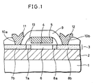
- Fig. 1 is a sectional view of a SOI-MOSFET as a first conventional example. Referring to Fig. 1, the SOI-MOSFET includes an
insulator layer 2 formed on asilicon substrate 1 and asilicon layer 3 formed oninsulator layer 2. Achannel forming region 6 having a low concentration of p-type impurities (10¹⁶ - 10¹⁷/cm³, for example) is formed insilicon layer 3, and anadditional source region 7a and anadditional drain region 8a having a concentration of n-type impurities (10¹⁷ - 10¹⁸/cm³, for example) are formed respectively in contact with the left and right sides ofchannel forming region 6. Asource region 7b and adrain region 8b having a high concentration of n-type impurities concentration (10¹⁹ - 10²¹/cm³, for example) are formed respectively adjacent toadditional source region 7a andadditional drain region 8a. - A
gate insulating film 4 is formed onchannel forming region 6, and agate electrode 5 is formed ongate insulating film 4.Sidewalls 13 are provided on the sidewalls ofgate electrode 5 onadditional source region 7a andadditional drain region 8a.Silicon layer 3 andgate electrode 5 are covered with aninterlayer insulating film 9. Contactholes 10a, 10b are provided in interlayerinsulating film 9, and corresponding conductors, i.e. asource electrode 11 and adrain electrode 12 in this case, are formed inrespective contact holes 10a, 10b. - If positive voltage is applied to
gate electrode 5 in a SOI-MOSFET constituted as described above, n-type carriers (electrons) are induced to the upper part of p-typechannel forming region 6, and the upper part is inverted to be the same n-type asadditional source region 7a,additional drain region 8a,source region 7b, anddrain region 8b. Accordingly, current can flow betweensource region 7b anddrain region 8b. In addition, the concentration of the n-type carriers induced to upper part ofchannel forming region 6 changes in accordance with the gate voltage, so that it is possible to control the current flowing inchannel forming region 6 with the gate voltage. This is the operation principle of the MOSFET. - The reason why
additional source region 7a andadditional drain region 8a were formed respectively adjacent tosource region 7b anddrain region 8b in the first conventional thin film SOI-MOSFET having the above-described structure is as described in the following. - In a case where it is a thin film SOI-MOSFET having
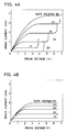
silicon layer 3 of approximately 300Å - 1500Å, even ifadditional source region 7a andadditional drain region 8a are not formed, the whole ofchannel forming region 6 is easily made to be a depletion layer by applying voltage togate electrode 5, and the potential of the channel forming region is also controlled by the gate electrode, so that so-called punch through or short channel effect is reduced. Here, "punch through" is a phenomenon that a depletion layer extending fromdrain region 8b intochannel forming region 6 reaches tosource region 7b, the electric barrier betweensource region 7b andchannel 6 is lowered, and the channel current is suddenly increased by it. "Short channel effect" is a phenomenon that when the gate length is short, the gate threshold voltage becomes extremely low. - However, if the whole of
channel forming region 6 is completely depleted, the potential inchannel forming region 6 becomes higher than that in the case of a conventional bulk MOSFET. Accordingly, the electric barrier betweensource region 7b andchannel forming region 6 is lowered, and holes generated by so-called impact ionization, a phenomenon that highly accelerated electrons collide with a lattice in the vicinity ofdrain region 8b and cause electrons and holes to be generated, come to be temporarily stored inchannel forming region 6. As a result, the potential inchannel forming region 6 is further raised, and electrons are suddenly injected fromsource region 7b intochannel forming region 6. Specifically, in a case whereadditional source region 7a andadditional drain region 8a are not formed in a thin film SOI-MOSFET expected as a short channel MOSFET, the withstand voltage between the source and the drain tends to be lowered. Fig. 4A shows the drain current - drain voltage characteristics of the thin film SOI-MOSFET in this case. - In order to prevent such lowering of the withstand voltage between the source and the drain, a so-called LDD (Lightly Doped Drain) structure is constituted by providing a low second conductivity-type
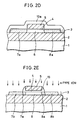
additional drain region 8a betweendrain region 8b andchannel forming region 6 in a normal thin film SOI-MOSFET such as the first conventional example described above to reduce the electric field in the vicinity ofdrain region 8b and prevent storage of holes caused by impact ionization so that the withstand voltage between the source and the drain is enhanced. Now, a method of manufacturing the above-described first conventional thin film SOI-MOSFET will be described with reference to Figs. 2A - 2E. - First, referring to Fig. 2A, a
silicon layer 3 is formed on asilicon substrate 1 with aninsulator layer 2 interposed therebetween. Specific manufacturing methods in this case normally include SIMOX (Separation by Implanted Oxygen) in which oxygen ions are implanted insilicon substrate 1 and a silicon oxide film is formed directly insilicon substrate 1. - Next,
silicon layer 3 is patterned into a shape of an island, and p-type impurities such as boron are introduced by an ion implantation process or the like to make the concentration 10¹⁶ - 10¹⁷/cm³, for example, to form a channel forming region 6 (Fig. 2B). - A
gate insulating film 4 is formed onsilicon layer 3 by a thermal oxidation process or the like, and a gate electrode material such as polycrystalline silicon is deposited by a CVD method. Aresist 14 is patterned on the polycrystalline silicon by a photolithography process, and the polycrystalline silicon is etched using theresist 14 to form agate electrode 5. - Next, n-type impurities such as phosphorus are introduced into
silicon layer 3 usinggate electrode 5 and resist 14 as a mask to make the concentration 10¹⁷ - 10¹⁸/cm³ to form anadditional source region 7a and anadditional drain region 8a (Fig. 2C). - Next, a
silicon oxide film 13a is deposited by a CVD method (Fig. 2D), anisotropic etching is carried out onsilicon oxide film 13a by a reactive ion etching process to form asidewall spacer 13 on the sidewalls ofgate electrode 5. Next, n-type impurities such as phosphorus or arsenic are ion-implanted insilicon layer 3 usinggate electrode 5 andsidewall spacer 13 as a mask, and asource region 7b and adrain region 8b are formed to have a concentration of 10¹⁹ - 10²¹/cm³, for example (Fig. 2E). - An
interlayer insulating film 9 is formed, thencontact holes 10a, 10b are formed by a reactive ion etching process, for example, andconductive interconnection layers - As described above, the above first conventional thin film SOI-MOSFET has the concentration of
additional source region 7a andadditional drain region 8a lowered to approximately 10¹⁷/cm³ in order to enhance the withstand voltage between the source and the drain by electric field reduction. Therefore, the carrier concentration is lowered, the resistance ofadditional source region 7a andadditional drain region 8a is increased, and a significant decline in the current driving capability is caused as shown in Fig. 4B. - Japanese Patent Laying-Open No. 60-133756 (1985) discloses a thin film SOI-MOSFET having a so-called gate overlap type LDD structure (hereinafter referred to as "a second conventional example"), for example, for improving the problems in the first conventional example.
- A thin film SOI-MOSFET of the second conventional example has low concentration impurity regions, which are additional source/drain regions, overlapped with the region of a gate electrode. This causes the gate voltage to be directly applied to the additional source/drain regions, so that it is possible to raise the carrier concentration of the additional source/drain regions at the same time that the conductivity type of the channel forming region is inverted when the MOSFET is on operation. Accordingly, it is possible to prevent deterioration of the current driving characteristics caused by increase of the resistance value of the additional source/drain regions having a low concentration.
- Now, a method of manufacturing the thin film SOI-MOSFET of the second conventional example will be described with reference to Figs. 3A to 3E.
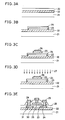
- First, referring to Fig. 3A, an
insulator layer 22 is formed on aninsulating substrate 21, and then asemiconductor layer 23 is formed. - Next, referring to Fig. 3B,
semiconductor layer 23 is patterned, and then agate insulating layer 24 is formed. Then, referring to Fig. 3C, agate electrode 25 having the resistance reduced by thermal diffusion of impurities or the like is formed, and then aresist layer 26 is etched so that it has the same width as the channel width and has a length shorter than the channel length by several percent as illustrated in Fig. 3C to form a mask for ion implantation as illustrated in Fig. 3C. - Next, referring to Fig. 3D, ion implantation is carried out by irradiating
impurity ions 27 usingresist layer 26 as a mask, and then heat treatment is carried out to activate the impurities. - Then, referring to Fig. 3E,
resist layer 26 is removed, and aninterlayer insulating layer 28 is formed. Contact holes are formed, and thenelectrodes 29 are formed. The concentration of an additional source/drain region 30 formed by ion implantation is lower than that of the region of a source/drain region 31 adjacent to it. This is because implantation of impurity ions into additional source/drain region 30 is carried out throughgate electrode 25, so that the amount of the implanted ions is reduced in accordance with effects of the thickness ofgate electrode 25. - However, according to the manufacturing method as described in the above second conventional example, ion implantation for forming additional source/
drain region 30 is carried out throughgate electrode 25, so that a step of forming resistlayer 26 is required, and the process becomes complicated. In addition, the concentration of additional source/drain region 30 is controlled by the thickness ofgate electrode 25, so that it is liable to be affected by diversification of the thickness or the material ofgate electrode 25. In the case of a thin film SOI-MOSFET of a LDD structure having an additional source/drain region overlapping withgate electrode 25, it is necessary to set the concentration of the additional source/drain region to a value in a certain limited range with high precision in order to obtain satisfactory transistor characteristics. However, there was no disclosure of a concentration setting in the above second conventional example, and fine control of the concentration of the additional source/drain region was difficult. - One object of the present invention is to provide a semiconductor device including a gate overlap-type thin film SOI-MOSFET having an optimum concentration of an additional source/drain region for having satisfactory transistor characteristics and a method of manufacturing the same.
- In order to solve the above described problems, a semiconductor device according to the present invention includes a semiconductor layer having a thickness of 300Å to 1500Å formed on an insulator layer and a gate electrode formed on the semiconductor layer with a gate insulating film interposed therebetween. A pair of additional source/drain regions of a first conductivity type is formed from immediately beneath both of right and left side ends of the gate electrode inward in the semiconductor layer in the region immediately beneath the gate electrode, and a channel forming region of a second conductivity type is formed in the semiconductor layer in a region between the pair of additional source/drain regions. Further, a pair of source/drain regions of the first conductivity type is formed adjacent to the end opposite the side in contact with the channel forming region of the additional source/drain regions in the semiconductor device.
- The additional source/drain regions in the semiconductor device have an impurity concentration of 3x10¹⁷ to 3x10¹⁸/cm³, and the source/drain region has an impurity concentration higher than that of the additional source/drain regions.
- According to the semiconductor device of the present invention, gate overlap-type additional source/drain regions are included, and the concentration is set to 3x10¹⁷ - 3x10¹⁸/cm³, so that it has functions as described in the following.
- In a case where the gate electrode is 0V, and a predetermined positive bias voltage is applied to the drain region, substantially only the whole of additional source/drain regions is depleted because the additional source/drain regions are set to have a concentration of 3x10¹⁸/cm³ or less. As a result, the electric field strength reduction effect is larger as compared to the case where the concentration of the additional source/drain regions is too high to sufficiently deplete the additional source/drain regions or the case where the concentration is so low as to cause depletion to proceed up to the adjacent source/drain regions. Further, it also has effects unique to a gate overlap structure, so that satisfactory transistor characteristics can be obtained. If the concentration of the additional source/drain region is set to less than 3x10¹⁷, the parasitic resistance thereof affects the properties of the device.
- According to a method of manufacturing a semiconductor device of the present invention, first, a gate insulating film is formed on a semiconductor layer on an insulator layer, and a gate electrode is formed on the gate insulating film. Next, impurities of a first conductivity type are introduced just beneath the vicinity of the ends of the gate electrode in the semiconductor layer by implanting the impurities from a predetermined direction making a predetermined angle of inclination with the surface of the semiconductor layer using the gate electrode as a mask to form additional source/drain regions. Subsequently, impurities of the first conductivity type are implanted from a direction perpendicular to the surface of the semiconductor layer onto the semiconductor layer using the gate electrode as a mask to form source/drain regions.
- According to the above-described manufacturing method, the additional source/drain regions are formed by ion implantation using only the gate electrode as a mask, so that it is not necessary to separately pattern the mask as in the above second conventional example, and the manufacturing process is simplified.
- According to another aspect of the method of manufacturing a semiconductor device of the present invention, the step of forming the additional source/drain regions is carried out by forming a gate electrode on the gate insulating film, then introducing impurities of a first conductivity type by ion implantation using the gate electrode as a mask, and then diffusing the impurities beneath the gate electrode by predetermined heat treatment.
- According to this manufacturing method, formation of the additional source/drain regions is carried out by oblique ion implantation using the gate electrode as a mask, so that it is possible to set the length of the overlap of the additional source/drain regions with the gate electrode or the impurity concentration with higher precision as compared to the case where it is carried out by thermal diffusion.
- The foregoing and other objects, features, aspects and advantages of the present invention will become more apparent from the following detailed description of the present invention when taken in conjunction with the accompanying drawings.
- Fig. 1 is a sectional view illustrating a sectional structure of a thin film SOI-MOSFET in a first conventional example.
- Figs. 2A, 2B, 2C, 2D and 2E are sectional views illustrating in sequence main steps of the method of manufacturing the semiconductor device in the first conventional example.
- Figs. 3A, 3B, 3C, 3D and 3E are sectional views illustrating in sequence a process of manufacturing a semiconductor device in a second conventional example.
- Fig. 4A is a graph showing the source/drain withstand voltage characteristics of a thin film SOI-MOSFET not having a LDD structure, and Fig. 4B is a graph showing the current characteristics of a LDD-type thin film SOI-MOSFET not having a gate overlap structure in the first conventional example.
- Figs. 5A, 5B, 5C, 5D and 5E are sectional views illustrating in sequence main steps of method of manufacturing a semiconductor device according to an embodiment of the present invention.
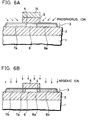
- Figs. 6A and 6B are sectional views illustrating main steps of a method of manufacturing a semiconductor device according to another embodiment of the present invention.
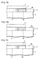
- Figs. 7A, 7B and 7C are typical sectional views illustrating the state of depletion of it in the non-operation state of a gate overlap-type thin film SOI-MOSFET.
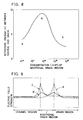
- Fig. 8 is a graph showing the relationship between the concentration of an additional drain region of a thin film SOI-MOSFET and the withstand voltage between the source and the drain.
- Fig. 9 is a graph showing distribution of electric strength in the vicinity of an additional drain region corresponding respectively to Figs. 7A, 7B and 7C.
- Figs. 10A and 10B are graphs showing the relationship between the concentration of additional source/drain regions of a thin film SOI-MOSFET and the voltage between the gate and the drain causing the additional drain region to be depleted completely in the case where the thickness of a silicon film is 300Å and in the case where it is. 1000Å.
- An embodiment of the present invention will be described in the following with reference to the drawings.
- The structure of a semiconductor device including a thin film SOI-MOSFET according to an embodiment of the present invention is substantially the same as that of the semiconductor device of the second conventional example illustrated in Fig. 3E. Specifically, referring to Fig. 5E, an
insulator layer 2 is formed on asilicon substrate 1, and asilicon layer 3 is formed oninsulator layer 2. Achannel forming region 6 having a low concentration of p-type impurities (10¹⁶ - 10¹⁷/cm³, for example) is formed insilicon layer 3. n-typeadditional source region 7a andadditional drain region 8a are formed overlapping with the vicinity of both of right and left ends of agate electrode 5 insilicon layer 3 which is in contact with both of left and right sides ofchannel forming region 6. n-type source region 7b and drainregion 8b having an impurity concentration higher than that ofadditional source region 7a andadditional drain region 8a are formed insilicon layer 3 adjacent to the ends oppositechannel forming region 6 ofadditional source region 7a andadditional drain region 8a. - The structure of the semiconductor device according to the present invention differs from the above-described second conventional example in that the concentration of
additional source region 7a,additional drain region 8a is set in the optimum range in accordance with the thickness ofsilicon layer 3. Specifically, according to this embodiment, it is a thin film SOI-MOSFET includingsilicon layer 3 having a thickness of 300 - 1500Å, and the concentration ofadditional source region 7a andadditional drain region 8a is set in the range of 3x10¹⁷ - 3x10¹⁸/cm³. - The reason why the concentration of
additional source region 7a andadditional drain region 8a is set in the above-described range in this embodiment will be described in the following. - The relationship between the concentration of
additional drain region 8a and the withstand voltage between the source and the drain is considered as described in the following with reference to Figs. 7A to 7C, 8 and 9. When the MOSFET is in the non-operation state, i.e. when a positive bias is applied to drainregion 8b and the gate electrode is 0V,additional drain region 8a is depleted. If the concentration ofadditional drain region 8a is lower than a predetermined value of approximately 10¹⁸/cm³, depletion proceeds up to drainregion 8b as indicated by oblique lines in Fig. 7A, and a peak of high electric field strength occurs in the vicinity of the boundary betweenadditional drain region 8a and drainregion 8b as indicated by arrow A in Fig. 9. The reason for this is considered to be that if the concentration ofadditional drain region 8a is too low, the effects of the region as a drain are lessened, and it is brought to a state substantially the same as the state in which the drain is moved to the right side. - If the concentration of
additional drain region 8a is of a predetermined value of approximately 10¹⁸,additional drain region 8a is depleted completely as indicated by oblique lines in Fig. 7B, and the peak of electric field strength is distributed in the vicinity of the both ends ofadditional drain region 8a as indicated by arrow B in Fig. 9, and the value of it becomes low. - In addition, in a case where the concentration of
additional drain region 8a is higher than a predetermined value of approximately 10¹⁸/cm³, depletion ofadditional drain region 8a proceeds only a little as illustrated by oblique lines in Fig. 7C, and therefore the field reduction effect inadditional drain region 8a is insufficient, and a high peak of electric strength occurs in the vicinity of its left end as indicated by arrow C in Fig. 9. - As seen from above results of consideration, the withstand voltage between the source and the drain of the SOI-MOSFET according to this embodiment becomes optimum when the concentration of
additional drain region 8a is set to approximately 10¹⁸ as shown by the graph in Fig. 8, and the withstand voltage between the source and the drain is lowered if the concentration is higher or lower than that. The graph in Fig. 8 shows the relationship between the concentration ofadditional drain region 8a and the withstand voltage between the source and the drain in a case where the length ofgate electrode 5 is 0.3µm, the thickness ofsilicon layer 3 is 300Å, and the thickness ofgate insulating film 4 is 200Å. - Now, the relationship between the thickness of
silicon layer 3 and the optimum concentration ofadditional drain region 8a, i.e. conditions for depleting completelyadditional drain region 8a will be considered. In a case where the thickness ofsilicon layer 3 is 300Å, in order to be adapted to a device structure in which the length ofgate electrode 5 is shorter than 0.3µm (so-called 0.3µm design rule),Additional drain region 8a must have an impurity concentration of approximately 3x10¹⁷ - 3x10¹⁸/cm³, because the supply voltage (the applied voltage to drainregion 8b) is normally 1 - 5V, and the thickness ofgate insulating film 4 is 100Å - 200Å (See Fig. 10A). On the other hand, in a case where the thickness ofsilicon layer 3 is 1000Å, the gate electrode length becomes approximately 0.5µm (so-called 0.5µm design rule), and the supply voltage (the applied voltage to drainregion 8b) normally becomes 3.3 - 5V. In this case, in order to deplete completelyadditional drain region 8a, it is necessary to set the impurity concentration to approximately 3x10¹⁷ - 5x10¹⁷/cm³ (See Fig. 10B). In a case where the thickness of the silicon layer is above 300Å and below 1000Å, it may be considered that it is in the middle condition of the above cases. - It is seen from the above description that the concentration of additional source/drain regions 7d, 8d of a thin film SOI-MOSFET including
silicon layer 3 having a thickness of approximately 300Å - 1500Å must be set in the range of 3x10¹⁷ - 3x10¹⁸/cm³. - Now, an embodiment of a method of manufacturing a semiconductor device including a gate overlap-type LDD MOSFET having the above structure will be described with reference to Figs. 5A to 5E.
- First, referring to Fig. 5A, a
silicon layer 3 as a semiconductor device is formed to have a thickness of 300Å - 1500Å on asilicon substrate 1 with aninsulator layer 2 interposed therebetween. Formation ofinsulator layer 2 is carried out by a SIMOX process in the same way as in the above first conventional example. - Next,
silicon layer 3 is processed into a shape of an island and p-type impurities such as boron are implanted to make the concentration 10¹⁶ - 1017/cm3, for example, using an ion implantation process or the like to form a channel forming region 6 (Fig. 5B). - Next, a
gate insulating film 4 is formed onsilicon layer 3 to have a thickness of approximately 200Å using a thermal oxidation process or the like, and then a layer of a gate electrode material such as polycrystalline silicon or the like is formed to have a thickness of approximately 2000Å using a CVD method or the like. A resist 14 is patterned on the polycrystalline silicon layer using a photolithography process, and the polycrystalline layer is etched using this as a mask to form agate electrode 5. Next, n-type impurities such as phosphorus ions are ion-implanted usinggate electrode 5 as a mask to form anadditional source region 7a and anadditional drain region 8a having a concentration of 3x10¹⁷ - 3x10¹⁸/cm³ (Fig. 5C). At this time, in a case where phosphorus is used as the impurities to be implanted and the thickness ofsilicon layer 3 is approximately 1000Å, implantation energy of approximately 30KeV and a dosage of 3x10¹³ - 3x10¹⁴/cm² are employed as ion implantation conditions for setting them to have the above concentration. - Next, predetermined heat treatment is carried out, and thermal diffusion causes
additional source region 7a,additional drain region 8a to move from immediately beneath the left and right side ends ofgate electrode 5 inward (Fig. 5D). A heat treatment condition for thermal diffusion in this case is that in the case where the thickness ofsilicon layer 3 is approximately 1000Å, heat treatment is carried out in a nitrogen atmosphere at approximately 1000°C for about one hour, so that thermal diffusion causesadditional source region 7a andadditional drain region 8a to move from immediately beneath the left and right side ends ofgate electrode 5 inward by approximately 1500Å. - Next, n-type impurities such as phosphorus ions or arsenic ions are implanted into
silicon layer 3 usinggate electrode 5 as a mask to form asource region 7b and adrain region 8b having a concentration of approximately 10¹⁹ - 10²⁰/cm³ (Fig. 5E). - Subsequently, an interlayer insulating film (not shown) is deposited on the whole surface of
silicon substrate 1, contact holes (not shown) are formed, and an interconnection layer (not shown) of aluminum or the like is formed to complete a thin film SOI-MOSFET having the same structure as the structure illustrated in Fig. 3E. - Now, another embodiment of a method of manufacturing a semiconductor device including a thin film SOI-MOSFET of a gate overlap-type LDD structure will be described with reference to Figs. 6A and 6B.
- According to this embodiment, the steps up to the step of forming a
silicon layer 3 as a semiconductor layer in a shape of an island are the same as those of the above embodiment illustrated in Figs. 5A and 5B. This embodiment differs from the above embodiment in that formation ofadditional source region 7a andadditional drain region 8a is carried out by irradiating ions, phosphorus ions, for example, from a direction making a predetermined angle of inclination with the surface ofsilicon layer 3, i.e. by using a so-called oblique ion implantation process as illustrated in Fig. 6A, so that the vicinity of the end ofgate electrode 5 overlaps withadditional source region 7a andadditional drain region 8a. According to the oblique ion implantation process, ion implantation is carried out withsilicon substrate 1 rotating in a plane parallel to its surface at a constant speed in order to form a pair ofadditional source region 7a andadditional drain region 8a on the left and right hands. In a case where the thickness ofsilicon layer 3 is approximately 1000Å and phosphorus ions are used as the impurities to be implanted, for setting the concentration ofadditional source region 7a andadditional drain region 8a to 3x10¹⁷ - 3x10¹⁸/cm³, ion implantation conditions are that the implantation energy is approximately 80KeV, the angle of inclination made between the ion irradiation direction and the direction of the normal ofsilicon layer 3 is approximately 60 degrees, and the dosage is 1.2x10¹³ - 1.2x10¹⁴/cm². These implantation conditions causeadditional source region 7a andadditional drain region 8a to move from both of the left and right side ends of the gate electrode inward by approximately 1500Å. - Next, photo resist 14 is removed, and arsenic ions, for example, are implanted from the direction perpendicular to the surface of
silicon layer 3 usinggate electrode 5 as a mask as in the case of the above embodiment (Fig. 5E) to form asource region 7b and adrain region 8b having a concentration of 10¹⁹ - 10²⁰/cm³. - While ion implantation is carried out with
silicon substrate 1 rotating for formingadditional source region 7a andadditional drain region 8a in this embodiment, it is possible to form them by carrying out ion implantation diagonally from the upper hand of one sidewall ofgate electrode 5 with a predetermined angle of inclination keepingsilicon substrate 1 still to form one ofadditional source region 7a andadditional drain region 8a, and then rotatingsilicon substrate 1 by 90 degrees in a plane parallel to its surface, fixing it, and carrying out ion implantation to form the other one ofadditional drain region 8a andadditional source region 7b. However, this method can be used only in the cases where a number of SOI-MOSFET elements on a silicon wafer are aligned in the same direction. - As described above, according to the structure of the semiconductor device of the above embodiment, the concentration of additional source/
drain regions gate electrode 5 is set to 3x10¹⁸/cm³ or less in the thin film SOI-MOSFET, so that additional source/drain regions drain regions - According to an embodiment of a method of manufacturing a semiconductor device of the present invention, the additional source/drain regions and the source/drain regions are formed using only the gate electrode as a mask, so that it is possible to form a SOI-MOSFET having a gate overlap-type LDD structure by a relatively simple process.
- Furthermore, according to another embodiment of a method of manufacturing a semiconductor device of the present invention, the additional source/drain regions are formed by using an oblique ion implantation process, so that it is possible to control the length of the gate overlap and the concentration of the additional source/drain regions with higher precision as compared to the case where a thermal diffusion step is included.
- Although the present invention has been described and illustrated in detail, it is clearly understood that the same is by way of illustration and example only and is not to be taken by way of limitation, the spirit and scope of the present invention being limited only by the terms of the appended claims.
Claims (16)
- A semiconductor device comprising:
a semiconductor layer (3) formed on an insulator (2) and having a thickness of 300Å to 1500Å;
a gate electrode (5) formed on said semiconductor layer (3) with a gate insulating film (4) interposed therebetween;
a pair of additional source/drain regions (7a, 8a) of a first conductivity type formed from immediately beneath both of the left and right side ends of said gate electrode (5) inward in said semiconductor layer (3) in a region immediately beneath said gate electrode (5);
A channel forming region (6) of a second conductivity type formed in said semiconductor layer (3) in a region between said pair of additional source/drain regions (7a, 8a); and
a pair of source/drain regions (7b, 8b) of the first conductivity type formed adjacent the ends opposite the sides of said additional source/drain regions (7a, 8a) in contact with said channel forming region (6) in said semiconductor layer (3);
said additional source/drain regions (7a, 8a) having an impurity concentration of 3x10¹⁷ to 3x10¹⁸/cm³; and
said source/drain regions (7b, 8b) having an impurity concentration higher than that of said additional source/drain regions (7a, 8a). - The semiconductor device according to claim 1, wherein said channel forming region (6) has a first conductivity-type impurity concentration of 10¹⁶ to 10¹⁷/cm³, and said source/drain regions (7b, 8b) has a second conductivity-type impurity concentration of 10¹⁹ to 10²⁰/cm³.
- The semiconductor device according to claim 1, wherein said silicon layer (3) has a thickness of 1000Å to 1500Å, and said additional source/drain regions (7a, 7b) has a second conductivity-type impurity concentration of 3x10¹⁷ to 5x10¹⁷/cm³.
- The semiconductor device according to claim 1, wherein said insulator (2) includes a silicon oxide film formed as buried by implanting oxygen ions, with a silicon layer (3) having a thickness of 300Å to 1500Å left from a main surface of silicon substrate (1), and to a predetermined depth from the lower surface of said silicon layer (3).
- The semiconductor device according to claim 1, wherein said semiconductor layer (3) is a silicon layer formed in a shape of an island on insulator (2).
- The semiconductor device according to claim 5, wherein
said channel forming region (6) is a p-type region including boron,
said additional source/drain regions (7a, 8a) are n-type regions including phosphorus, and
said source/drain regions (7b, 8b) are n-type regions including phosphorus or arsenic. - The semiconductor device according to claim 6, wherein
said channel forming region (6) has an impurity concentration of 10¹⁶ to 10¹⁷/cm³, and
said source/drain regions (7b, 8b) have an impurity concentration of 10¹⁹ to 10²⁰/cm³. - A method of manufacturing a semiconductor device comprising the steps of:
forming a semiconductor layer (3) on an insulator (2);
forming a gate insulating film (4) on said semiconductor layer (3);
forming a gate electrode (5) on said gate insulating film (4);
introducing impurities of a conductivity type immediately beneath the vicinity of the ends of said gate electrode (5) in said semiconductor layer (3) by implanting them from a predetermined direction making a predetermined angle of inclination with the surface of said semiconductor layer (3) using said gate electrode (5) as a mask to form additional source/drain regions (7a, 8a); and
implanting impurities of the same conductivity type as that of the impurities implanted into said additional source/drain regions (7a, 8a) from a direction perpendicular to the surface of said semiconductor layer (3) into said semiconductor layer (3) using said gate electrode (5) as a mask to form source/drain regions (7b, 8b). - The method of manufacturing a semiconductor device according to claim 8, wherein said step of forming said additional source/drain regions (7a, 8a) includes the step of implanting impurities of said conductivity type from a predetermined direction making a predetermined angle of inclination with the surface of said semiconductor layer (3) with said semiconductor layer (3) rotated continuously in a plane parallel to its surface.
- The method of manufacturing a semiconductor device according to claim 8, wherein
said step of forming said additional source/drain regions (7a, 8a) includes;
a first step of implanting impurities of said conductivity type from a predetermined direction making a predetermined angle of inclination with the surface of said semiconductor layer (3) with said semiconductor layer (3) kept still, and
a second step of rotating said semiconductor layer (3) by 180° relatively to said direction of implanting impurities of said conductivity type in a plane parallel to its surface, and then implanting impurities of said conductivity type again from the same direction as the one in said first step with said semiconductor layer (3) kept still. - A method of manufacturing a semiconductor device comprising the steps of:
forming a semiconductor layer (3) on an insulator (2);
forming a gate insulating film (4) on said semiconductor layer (3);
forming a gate electrode (5) on said gate insulating film (4);
introducing impurities of a first conductivity type by ion implantation using said gate electrode (5) as a mask;
diffusing the implanted impurities of the first conductivity type beneath said gate electrode (5) by predetermined heat treatment to form additional source/drain regions (7a, 7b); and
implanting impurities of said first conductivity type into said semiconductor layer (3) using said gate electrode (5) as a mask to form source/drain regions (7b, 8b). - The method of manufacturing a semiconductor device according to claim 11, wherein said predetermined heat treatment in said step of forming said additional source/drain regions (7a, 8a) is carried out in a nitrogen atmosphere at substantially 1000oC. for a predetermined time.
- The method of manufacturing a semiconductor device according to either of claims 8 or 11, wherein said step of forming said semiconductor layer (3) on said insulator (2) includes the step of implanting oxygen ions into a main surface of a silicon substrate for forming a silicon oxide film (2) as buried to be said insulator (2), with a silicon layer (3) having a thickness of 300Å to 1500Å left from the main surface of said silicon substrate, and to a predetermined depth from the lower surface of said silicon layer (3).
- The method of manufacturing a semiconductor device according to either of claims 8 or 11, wherein
said step of forming said semiconductor layer (3) on said insulator (2) includes the steps of:
forming a silicon layer (3) in a shape of an island on said insulator (2), and
implanting impurities of a second conductivity type into said silicon layer (3). - The method of manufacturing a semiconductor device according to claim 14, wherein said step of implanting impurities of the second conductivity type onto said silicon layer (3) includes the step of implanting boron to make the concentration 10¹⁶ to 10¹⁷/cm³.
- The method of manufacturing a semiconductor device according to either of claims 8 or 11, wherein phosphorus is implanted in said step of forming said additional source/drain regions (7a, 8a), and phosphorus or arsenic is implanted to make the concentration 10¹⁹ to 10²⁰/cm³ in said step of forming said source/drain regions (7b, 8b).
Applications Claiming Priority (2)
| Application Number | Priority Date | Filing Date | Title |
|---|---|---|---|
| JP314544/90 | 1990-11-19 | ||
| JP2314544A JP2660451B2 (en) | 1990-11-19 | 1990-11-19 | Semiconductor device and manufacturing method thereof |
Publications (3)
| Publication Number | Publication Date |
|---|---|
| EP0487220A2 true EP0487220A2 (en) | 1992-05-27 |
| EP0487220A3 EP0487220A3 (en) | 1992-07-29 |
| EP0487220B1 EP0487220B1 (en) | 1997-01-02 |
Family
ID=18054572
Family Applications (1)
| Application Number | Title | Priority Date | Filing Date |
|---|---|---|---|
| EP91310089A Expired - Lifetime EP0487220B1 (en) | 1990-11-19 | 1991-10-31 | SOI-Field effect transistor and method of manufacturing the same |
Country Status (4)
| Country | Link |
|---|---|
| US (1) | US6358783B1 (en) |
| EP (1) | EP0487220B1 (en) |
| JP (1) | JP2660451B2 (en) |
| DE (1) | DE69123950T2 (en) |
Cited By (15)
| Publication number | Priority date | Publication date | Assignee | Title |
|---|---|---|---|---|
| EP0643419A2 (en) * | 1993-08-31 | 1995-03-15 | STMicroelectronics, Inc. | Integrated circuit transistor having drain junction offset |
| EP0704909A2 (en) * | 1994-09-30 | 1996-04-03 | STMicroelectronics, Inc. | MOS-type semiconductor device and method for making the same |
| GB2309823A (en) * | 1995-12-30 | 1997-08-06 | Hyundai Electronics Ind | SOI semiconductor device and method of fabricating the same |
| EP0803911A3 (en) * | 1996-04-25 | 1998-04-15 | Sharp Kabushiki Kaisha | Channel structure of field effect transistor and CMOS element |
| CN1050700C (en) * | 1995-06-20 | 2000-03-22 | 现代电子产业株式会社 | Transistor in semiconductor device and method of making the same |
| CN1050701C (en) * | 1995-06-20 | 2000-03-22 | 现代电子产业株式会社 | Transistor in semiconductor device and method of making the same |
| EP1028469A2 (en) * | 1999-02-12 | 2000-08-16 | Sel Semiconductor Energy Laboratory Co., Ltd. | Semiconductor device and method of manufacturing the same |
| US6291325B1 (en) * | 1998-11-18 | 2001-09-18 | Sharp Laboratories Of America, Inc. | Asymmetric MOS channel structure with drain extension and method for same |
| US6507069B1 (en) | 1994-07-14 | 2003-01-14 | Semiconductor Energy Laboratory Co., Ltd. | Semiconductor device and method of manufacture thereof |
| US6777763B1 (en) * | 1993-10-01 | 2004-08-17 | Semiconductor Energy Laboratory Co., Ltd. | Semiconductor device and method for fabricating the same |
| US6906383B1 (en) | 1994-07-14 | 2005-06-14 | Semiconductor Energy Laboratory Co., Ltd. | Semiconductor device and method of manufacture thereof |
| EP1564800A3 (en) * | 1993-09-20 | 2006-03-15 | Semiconductor Energy Laboratory Co., Ltd. | Semiconductor device and method for manufacturing the same |
| EP1033755A3 (en) * | 1999-03-04 | 2009-09-23 | Sel Semiconductor Energy Laboratory Co., Ltd. | Semiconductor device and manufacturing method thereof |
| US8357611B2 (en) | 1999-06-22 | 2013-01-22 | Semiconductor Energy Laboratory Co., Ltd. | Wiring material, semiconductor device provided with a wiring using the wiring material and method of manufacturing thereof |
| CN109888021A (en) * | 2019-02-27 | 2019-06-14 | 京东方科技集团股份有限公司 | A kind of thin film transistor (TFT) and preparation method thereof, array substrate, display device |
Families Citing this family (7)
| Publication number | Priority date | Publication date | Assignee | Title |
|---|---|---|---|---|
| EP0650190B1 (en) * | 1993-10-26 | 2000-10-04 | International Business Machines Corporation | Single event upset hardening of commercial VLSI technology without circuit redesign |
| US6524895B2 (en) | 1998-12-25 | 2003-02-25 | Semiconductor Energy Laboratory Co., Ltd. | Semiconductor device and method of fabricating the same |
| JP4850326B2 (en) * | 1999-03-26 | 2012-01-11 | 株式会社半導体エネルギー研究所 | Method for manufacturing semiconductor device |
| JP4766724B2 (en) * | 1999-06-22 | 2011-09-07 | 株式会社半導体エネルギー研究所 | Method for manufacturing semiconductor device |
| JP2002185011A (en) * | 2000-12-19 | 2002-06-28 | Seiko Epson Corp | Semiconductor device |
| JP3634320B2 (en) * | 2002-03-29 | 2005-03-30 | 株式会社東芝 | Semiconductor device and manufacturing method of semiconductor device |
| JP2004079735A (en) * | 2002-08-15 | 2004-03-11 | Nec Corp | Method of manufacturing thin film transistor |
Citations (2)
| Publication number | Priority date | Publication date | Assignee | Title |
|---|---|---|---|---|
| JPS6276776A (en) * | 1985-09-30 | 1987-04-08 | Toshiba Corp | Semiconductor device |
| EP0373893A2 (en) * | 1988-12-13 | 1990-06-20 | Mitsubishi Denki Kabushiki Kaisha | MOS type field effect transistor formed on a semiconductor layer on an insulator substrate |
Family Cites Families (16)
| Publication number | Priority date | Publication date | Assignee | Title |
|---|---|---|---|---|
| US4087902A (en) | 1976-06-23 | 1978-05-09 | The United States Of America As Represented By The Administrator Of The National Aeronautics And Space Administration | Field effect transistor and method of construction thereof |
| JPS58142566A (en) * | 1982-02-19 | 1983-08-24 | Seiko Epson Corp | Thin film semiconductor device |
| JPS60133756A (en) | 1983-12-21 | 1985-07-16 | Seiko Epson Corp | Manufacture of thin film transistor |
| JPS61104671A (en) | 1984-10-29 | 1986-05-22 | Sharp Corp | Field effect transistor |
| US4649629A (en) * | 1985-07-29 | 1987-03-17 | Thomson Components - Mostek Corp. | Method of late programming a read only memory |
| US4922315A (en) | 1987-11-13 | 1990-05-01 | Kopin Corporation | Control gate lateral silicon-on-insulator bipolar transistor |
| JPH01307266A (en) * | 1988-06-06 | 1989-12-12 | Hitachi Ltd | Manufacture of semiconductor device |
| JPH0227772A (en) | 1988-07-15 | 1990-01-30 | Sony Corp | Field effect type thin film transistor |
| JP3143102B2 (en) * | 1988-09-09 | 2001-03-07 | ソニー株式会社 | MIS type transistor |
| JP2507567B2 (en) | 1988-11-25 | 1996-06-12 | 三菱電機株式会社 | MOS field effect transistor formed in semiconductor layer on insulator substrate |
| JPH0783127B2 (en) | 1989-04-20 | 1995-09-06 | 三菱電機株式会社 | Semiconductor device |
| JPH03129764A (en) | 1989-05-26 | 1991-06-03 | Fuji Electric Co Ltd | Semiconductor device |
| US5158903A (en) * | 1989-11-01 | 1992-10-27 | Matsushita Electric Industrial Co., Ltd. | Method for producing a field-effect type semiconductor device |
| US5241211A (en) * | 1989-12-20 | 1993-08-31 | Nec Corporation | Semiconductor device |
| US5102809A (en) | 1990-10-11 | 1992-04-07 | Texas Instruments Incorporated | SOI BICMOS process |
| JP2735041B2 (en) * | 1995-07-28 | 1998-04-02 | 日本電気株式会社 | Semiconductor device and manufacturing method thereof |
-
1990
- 1990-11-19 JP JP2314544A patent/JP2660451B2/en not_active Expired - Lifetime
-
1991
- 1991-10-31 DE DE69123950T patent/DE69123950T2/en not_active Expired - Fee Related
- 1991-10-31 EP EP91310089A patent/EP0487220B1/en not_active Expired - Lifetime
-
1999
- 1999-01-20 US US09/233,212 patent/US6358783B1/en not_active Expired - Fee Related
Patent Citations (2)
| Publication number | Priority date | Publication date | Assignee | Title |
|---|---|---|---|---|
| JPS6276776A (en) * | 1985-09-30 | 1987-04-08 | Toshiba Corp | Semiconductor device |
| EP0373893A2 (en) * | 1988-12-13 | 1990-06-20 | Mitsubishi Denki Kabushiki Kaisha | MOS type field effect transistor formed on a semiconductor layer on an insulator substrate |
Non-Patent Citations (3)
| Title |
|---|
| 1988 SYPOSIUM ON VLSI TECHNOLOGY 10 May 1988, SAN DIEGO USA pages 15 - 16; T. HORI ET AL.: 'a new submicron mosfet with latid (large-tilt-angle implanted drain) structure' * |
| NUCLEAR INSTRUMENTS AND METHODS IN PHYSICS RESEARCH /B vol. 37/38, no. 2, February 1989, AMSTERDAM NETHERLANDS pages 9 - 15; Y. AKASAKA: 'current status of ion implantation for vlsi applications' * |
| PATENT ABSTRACTS OF JAPAN vol. 11, no. 277 (E-538)(2724) 8 September 1987 & JP-A-62 076 776 ( TOSHIBA ) 8 April 1987 * |
Cited By (29)
| Publication number | Priority date | Publication date | Assignee | Title |
|---|---|---|---|---|
| EP0643419A2 (en) * | 1993-08-31 | 1995-03-15 | STMicroelectronics, Inc. | Integrated circuit transistor having drain junction offset |
| EP0643419A3 (en) * | 1993-08-31 | 1996-02-28 | Sgs Thomson Microelectronics | Integrated circuit transistor having drain junction offset. |
| US7847355B2 (en) * | 1993-09-20 | 2010-12-07 | Semiconductor Energy Laboratory Co., Ltd. | Semiconductor device including transistors with silicided impurity regions |
| US7525158B2 (en) * | 1993-09-20 | 2009-04-28 | Semiconductor Energy Laboratory Co., Ltd. | Semiconductor device having pixel electrode and peripheral circuit |
| EP1564800A3 (en) * | 1993-09-20 | 2006-03-15 | Semiconductor Energy Laboratory Co., Ltd. | Semiconductor device and method for manufacturing the same |
| US7166503B2 (en) | 1993-10-01 | 2007-01-23 | Semiconductor Energy Laboratory Co., Ltd. | Method of manufacturing a TFT with laser irradiation |
| US6777763B1 (en) * | 1993-10-01 | 2004-08-17 | Semiconductor Energy Laboratory Co., Ltd. | Semiconductor device and method for fabricating the same |
| US6773971B1 (en) | 1994-07-14 | 2004-08-10 | Semiconductor Energy Laboratory Co., Ltd. | Method of manufacturing a semiconductor device having lightly-doped drain (LDD) regions |
| US7635895B2 (en) | 1994-07-14 | 2009-12-22 | Semiconductor Energy Laboratory Co., Ltd. | Display device |
| US8273613B2 (en) | 1994-07-14 | 2012-09-25 | Semiconductor Energy Laboratory Co., Ltd. | Semiconductor device and method of manufacture thereof |
| US7183614B2 (en) | 1994-07-14 | 2007-02-27 | Semiconductor Energy Laboratory Co., Ltd. | Semiconductor device and method of manufacture thereof |
| US6906383B1 (en) | 1994-07-14 | 2005-06-14 | Semiconductor Energy Laboratory Co., Ltd. | Semiconductor device and method of manufacture thereof |
| US6507069B1 (en) | 1994-07-14 | 2003-01-14 | Semiconductor Energy Laboratory Co., Ltd. | Semiconductor device and method of manufacture thereof |
| EP0704909A3 (en) * | 1994-09-30 | 1997-09-10 | Sgs Thomson Microelectronics | MOS-type semiconductor device and method for making the same |
| US5801397A (en) * | 1994-09-30 | 1998-09-01 | Sgs-Thomson Microelectronics, Inc. | Device having a self-aligned gate electrode wrapped around the channel |
| EP0704909A2 (en) * | 1994-09-30 | 1996-04-03 | STMicroelectronics, Inc. | MOS-type semiconductor device and method for making the same |
| CN1050701C (en) * | 1995-06-20 | 2000-03-22 | 现代电子产业株式会社 | Transistor in semiconductor device and method of making the same |
| CN1050700C (en) * | 1995-06-20 | 2000-03-22 | 现代电子产业株式会社 | Transistor in semiconductor device and method of making the same |
| GB2309823A (en) * | 1995-12-30 | 1997-08-06 | Hyundai Electronics Ind | SOI semiconductor device and method of fabricating the same |
| GB2309823B (en) * | 1995-12-30 | 2000-11-15 | Hyundai Electronics Ind | Semiconductor device and method of fabricating the same |
| EP0803911A3 (en) * | 1996-04-25 | 1998-04-15 | Sharp Kabushiki Kaisha | Channel structure of field effect transistor and CMOS element |
| US5841170A (en) * | 1996-04-25 | 1998-11-24 | Sharp Kabushiki Kaisha | Field effect transistor and CMOS element having dopant exponentially graded in channel |
| US6291325B1 (en) * | 1998-11-18 | 2001-09-18 | Sharp Laboratories Of America, Inc. | Asymmetric MOS channel structure with drain extension and method for same |
| EP1028469A2 (en) * | 1999-02-12 | 2000-08-16 | Sel Semiconductor Energy Laboratory Co., Ltd. | Semiconductor device and method of manufacturing the same |
| EP1028469A3 (en) * | 1999-02-12 | 2009-04-15 | Sel Semiconductor Energy Laboratory Co., Ltd. | Semiconductor device and method of manufacturing the same |
| EP1033755A3 (en) * | 1999-03-04 | 2009-09-23 | Sel Semiconductor Energy Laboratory Co., Ltd. | Semiconductor device and manufacturing method thereof |
| US8357611B2 (en) | 1999-06-22 | 2013-01-22 | Semiconductor Energy Laboratory Co., Ltd. | Wiring material, semiconductor device provided with a wiring using the wiring material and method of manufacturing thereof |
| US9660159B2 (en) | 1999-06-22 | 2017-05-23 | Semiconductor Energy Laboratory Co., Ltd. | Wiring material, semiconductor device provided with a wiring using the wiring material and method of manufacturing thereof |
| CN109888021A (en) * | 2019-02-27 | 2019-06-14 | 京东方科技集团股份有限公司 | A kind of thin film transistor (TFT) and preparation method thereof, array substrate, display device |
Also Published As
| Publication number | Publication date |
|---|---|
| JPH04188633A (en) | 1992-07-07 |
| DE69123950D1 (en) | 1997-02-13 |
| EP0487220A3 (en) | 1992-07-29 |
| EP0487220B1 (en) | 1997-01-02 |
| US6358783B1 (en) | 2002-03-19 |
| JP2660451B2 (en) | 1997-10-08 |
| DE69123950T2 (en) | 1997-05-28 |
Similar Documents
| Publication | Publication Date | Title |
|---|---|---|
| US6358783B1 (en) | Semiconductor device and method of manufacturing the same | |
| US6287906B1 (en) | Semiconductor device having MOS transistor and method of manufacturing the same | |
| US4680603A (en) | Graded extended drain concept for reduced hot electron effect | |
| US5583067A (en) | Inverse T-gate semiconductor device with self-aligned punchthrough stops and method of fabrication | |
| US5510279A (en) | Method of fabricating an asymmetric lightly doped drain transistor device | |
| EP1058303A1 (en) | Fabrication of VDMOS structure with reduced parasitic effects | |
| US4859620A (en) | Graded extended drain concept for reduced hot electron effect | |
| EP0583897B1 (en) | Field-effect transistor with structure for suppressing hot-electron effects, and method of fabricating the transistor | |
| US4613882A (en) | Hybrid extended drain concept for reduced hot electron effect | |
| KR19980085261A (en) | Semiconductor device and manufacturing method thereof | |
| US6300207B1 (en) | Depleted sidewall-poly LDD transistor | |
| US5212542A (en) | Semiconductor device having at least two field effect transistors and method of manufacturing the same | |
| US4691433A (en) | Hybrid extended drain concept for reduced hot electron effect | |
| KR900008153B1 (en) | Semiconductor device and its manufacturing method | |
| US5502322A (en) | Transistor having a nonuniform doping channel | |
| JPS60247974A (en) | Semiconductor device | |
| KR100257074B1 (en) | Mosfet and method for manufacturing the same | |
| EP0197501A2 (en) | Extended drain concept for reduced hot electron effect | |
| JP2880885B2 (en) | Semiconductor integrated circuit device and method of manufacturing the same | |
| KR0174569B1 (en) | Semiconductor device and method of manufacturing the same | |
| JP2608627B2 (en) | Method for manufacturing semiconductor device | |
| JP2765142B2 (en) | Method for manufacturing semiconductor device | |
| JPH08172193A (en) | Semiconductor device | |
| JPH0786307A (en) | Field effect transistor and its manufacture | |
| KR19980066763A (en) | Semiconductor element and manufacturing method thereof |
Legal Events
| Date | Code | Title | Description |
|---|---|---|---|
| PUAI | Public reference made under article 153(3) epc to a published international application that has entered the european phase |
Free format text: ORIGINAL CODE: 0009012 |
|
| AK | Designated contracting states |
Kind code of ref document: A2 Designated state(s): DE FR GB |
|
| PUAL | Search report despatched |
Free format text: ORIGINAL CODE: 0009013 |
|
| AK | Designated contracting states |
Kind code of ref document: A3 Designated state(s): DE FR GB |
|
| 17P | Request for examination filed |
Effective date: 19930125 |
|
| 17Q | First examination report despatched |
Effective date: 19941012 |
|
| GRAG | Despatch of communication of intention to grant |
Free format text: ORIGINAL CODE: EPIDOS AGRA |
|
| GRAH | Despatch of communication of intention to grant a patent |
Free format text: ORIGINAL CODE: EPIDOS IGRA |
|
| GRAH | Despatch of communication of intention to grant a patent |
Free format text: ORIGINAL CODE: EPIDOS IGRA |
|
| GRAA | (expected) grant |
Free format text: ORIGINAL CODE: 0009210 |
|
| AK | Designated contracting states |
Kind code of ref document: B1 Designated state(s): DE FR GB |
|
| REF | Corresponds to: |
Ref document number: 69123950 Country of ref document: DE Date of ref document: 19970213 |
|
| ET | Fr: translation filed | ||
| PLBE | No opposition filed within time limit |
Free format text: ORIGINAL CODE: 0009261 |
|
| STAA | Information on the status of an ep patent application or granted ep patent |
Free format text: STATUS: NO OPPOSITION FILED WITHIN TIME LIMIT |
|
| 26N | No opposition filed | ||
| REG | Reference to a national code |
Ref country code: GB Ref legal event code: IF02 |
|
| PGFP | Annual fee paid to national office [announced via postgrant information from national office to epo] |
Ref country code: DE Payment date: 20081027 Year of fee payment: 18 |
|
| PGFP | Annual fee paid to national office [announced via postgrant information from national office to epo] |
Ref country code: FR Payment date: 20081014 Year of fee payment: 18 |
|
| PGFP | Annual fee paid to national office [announced via postgrant information from national office to epo] |
Ref country code: GB Payment date: 20081029 Year of fee payment: 18 |
|
| REG | Reference to a national code |
Ref country code: FR Ref legal event code: ST Effective date: 20100630 |
|
| PG25 | Lapsed in a contracting state [announced via postgrant information from national office to epo] |
Ref country code: FR Free format text: LAPSE BECAUSE OF NON-PAYMENT OF DUE FEES Effective date: 20091102 Ref country code: DE Free format text: LAPSE BECAUSE OF NON-PAYMENT OF DUE FEES Effective date: 20100501 |
|
| PG25 | Lapsed in a contracting state [announced via postgrant information from national office to epo] |
Ref country code: GB Free format text: LAPSE BECAUSE OF NON-PAYMENT OF DUE FEES Effective date: 20091031 |