EP0487984A2 - Filtered plug connector - Google Patents
Filtered plug connector Download PDFInfo
- Publication number
- EP0487984A2 EP0487984A2 EP91119414A EP91119414A EP0487984A2 EP 0487984 A2 EP0487984 A2 EP 0487984A2 EP 91119414 A EP91119414 A EP 91119414A EP 91119414 A EP91119414 A EP 91119414A EP 0487984 A2 EP0487984 A2 EP 0487984A2
- Authority
- EP
- European Patent Office
- Prior art keywords
- housing
- plate
- capacitor
- ground plate
- plug connector
- Prior art date
- Legal status (The legal status is an assumption and is not a legal conclusion. Google has not performed a legal analysis and makes no representation as to the accuracy of the status listed.)
- Granted
Links
Images
Classifications
-
- H—ELECTRICITY
- H01—ELECTRIC ELEMENTS
- H01R—ELECTRICALLY-CONDUCTIVE CONNECTIONS; STRUCTURAL ASSOCIATIONS OF A PLURALITY OF MUTUALLY-INSULATED ELECTRICAL CONNECTING ELEMENTS; COUPLING DEVICES; CURRENT COLLECTORS
- H01R13/00—Details of coupling devices of the kinds covered by groups H01R12/70 or H01R24/00 - H01R33/00
- H01R13/66—Structural association with built-in electrical component
- H01R13/719—Structural association with built-in electrical component specially adapted for high frequency, e.g. with filters
- H01R13/7195—Structural association with built-in electrical component specially adapted for high frequency, e.g. with filters with planar filters with openings for contacts
-
- H—ELECTRICITY
- H01—ELECTRIC ELEMENTS
- H01R—ELECTRICALLY-CONDUCTIVE CONNECTIONS; STRUCTURAL ASSOCIATIONS OF A PLURALITY OF MUTUALLY-INSULATED ELECTRICAL CONNECTING ELEMENTS; COUPLING DEVICES; CURRENT COLLECTORS
- H01R12/00—Structural associations of a plurality of mutually-insulated electrical connecting elements, specially adapted for printed circuits, e.g. printed circuit boards [PCB], flat or ribbon cables, or like generally planar structures, e.g. terminal strips, terminal blocks; Coupling devices specially adapted for printed circuits, flat or ribbon cables, or like generally planar structures; Terminals specially adapted for contact with, or insertion into, printed circuits, flat or ribbon cables, or like generally planar structures
- H01R12/70—Coupling devices
- H01R12/71—Coupling devices for rigid printing circuits or like structures
- H01R12/72—Coupling devices for rigid printing circuits or like structures coupling with the edge of the rigid printed circuits or like structures
- H01R12/722—Coupling devices for rigid printing circuits or like structures coupling with the edge of the rigid printed circuits or like structures coupling devices mounted on the edge of the printed circuits
- H01R12/724—Coupling devices for rigid printing circuits or like structures coupling with the edge of the rigid printed circuits or like structures coupling devices mounted on the edge of the printed circuits containing contact members forming a right angle
Definitions
- the invention relates to an electrical connector and, in particular to a plug comprising a housing, a ground plate lying on the inside thereof, bores passing through the housing and openings in the ground plate, plug pins which pass through the bores and the openings and which are held in the former, and multi-layer ceramic capacitors which are arranged on the inside of the housing and which are disposed electrically between the ground plate and the plug pins.
- Plugs are known, one of which is shown, for example, in U.S. 4,930,200, to Brush, et al.
- Plugs of that kind serve for connecting printed circuit boards to other electrical components.
- the plug pins thereof are inserted with their one ends into the metallized holes in the printed circuit board. Their other ends extend for example to the wires of a cable.
- high-frequency signals or interference signals are to be removed.
- the multi-layer ceramic capacitors which are disposed between a ground plate and the plug pins are provided for that purpose.
- the capacitors are of dimensions of only a very few millimeters and they are arranged on a printed circuit board which is fixed in the plug.
- the invention is based on the provision of a plug in which high-frequency interference signals are carried away to ground and the multi-layer ceramic capacitors of which are not subjected to a mechanical loading and which can also be produced cost effectively.
- the solution to that problem is achieved in a plug of the kind set forth in the opening part of this specification, in accordance with the invention, in that the multi-layer ceramic capacitors are resiliently clamped between the ground plate and the plug pins.
- the multi-layer ceramic capacitors are disposed directly between the ground plate and the plug pins and are resiliently clamped between same and are not fitted onto an additional component, such as a printed circuit board.
- an additional component such as a printed circuit board.
- Such arrangement therefore omits the rigid connection to the printed circuit board and the resulting risk of breakage.
- the arrangement also omits the printed circuit board itself, as an additional cost-incurring component.
- the elasticity of the ground plate is considered sufficient to clamp the multi-layer ceramic capacitors in position resiliently and nonetheless securely.
- the capacitors are sufficiently securely held in place from the mechanical point of view.
- the pressure applied by the ground plate is also sufficient to provide a sound electrical connection.
- the manner in which the multi-layer ceramic capacitors are held in position between the plug pins on one side and the ground plate on the other side is not rigid. As such, the multi-layer ceramic capacitors do not follow all possible movements, and as a result they are not subjected to a mechanical loading and the risk of breakage is reduced.
- a desirable configuration provides that the openings in the ground plate are surrounded by plate portions which are bent out of the ground plate towards the housing.
- the height of such plate portions corresponds at least to the thickness of the multi-layer ceramic capacitors, and the latter are clamped between the plate portions and the plug pins.
- the plate portions have a flat section extending parallel to the end faces of the multi-layer ceramic capacitors. The length of the plate portions approximately corresponds to the height or thickness of the multi-layer ceramic capacitors. The flat section bears against the end faces or metallized ends of the multi-layer ceramic capacitors.
- a further desirable configuration provides that disposed on the inside of the housing are recesses and the plate portions are bent into said recesses.
- a plate lies on the ground plate, the plate having protrusions which are aligned with the openings in the ground plate and the multi-layer ceramic capacitors and bearing against the capacitors. The protrusions of the plate additionally fix the multi-layer ceramic capacitors. Likewise they additionally fix the ground plate.
- the multi-layer ceramic capacitors may be arranged on one or both sides of the plug pins.
- the housing When a multi-layer ceramic capacitor is disposed only on one side of the plug pin, desirably, at the side of the plug pin which is remote from the multi-layer ceramic capacitor, the housing has a support which bears against the plug pin. In addition at the side of the multi-layer ceramic capacitor which is remote from the protrusion of the plate, the housing may have a support which bears against the capacitor.
- the supports are formed integrally with the housing. The first-mentioned support bears against a plug pin and the additionally mentioned support bears against a multi-layer ceramic capacitor. By virtue of that arrangement those components are additionally supported and fixed in position.
- plugs may also be soldered with one of their metallized ends to a plug pin and with their other metallized end to the inwardly bent plate portions of the ground plate.
- the plugs are exposed to shocks, shaking movements and/or vibration.
- an embodiment is recommended in accordance with the invention in which depressions are provided on the inside of the housing to receive the multi-layer ceramic capacitors and the latter are disposed in the depressions.
- the dimensions of the depressions are so matched to those of the multi-layer ceramic capacitors that they are positively held in the depressions.
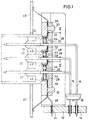
- Figure 1 shows a part of a printed circuit board 12 with metallized holes 14. Plug pins 16 are fitted into the latter. Some of the plug pins 16 are held together and fixed with a plate portion 18.
- FIG 1 shows the housing 20, insofar as is essential for the present invention. Bores 22 pass through the housing 20 and accommodate the plug pins 16.
- a plate 26 lies on the inside 24 of the housing 20, with the interposition of the ground plate which is to be described hereinafter.
- the plate 26 has protrusions 28. The protrusions 28 bear against the multi-layer ceramic capacitors which are to be described hereinafter.
- Figure 1 also shows rivet heads 30 which are formed integrally with the housing 20. They pass through openings in the plate 26 and fix the plate 26 to the housing 20.
- Figure 1 shows three plug pins 16.
- the multi-layer ceramic capacitors to be described hereinafter are disposed only at the top side thereof.
- the multi-layer ceramic capacitors are disposed on both sides thereof.
- the housing 20 has supports 32 which are formed integrally therewith. The supports 32 engage under and fix the plug pins 16. In that way the pins are protected from being bent.
- the housing further has supports or protuberances 34.
- the supports 34 are also formed integrally with the housing 20 and bear against the left-hand side of the multi-layer ceramic capacitors. In that way the capacitors are fixed in a lateral direction between the protrusions 28 and the supports 34.
- a ground plate 36 lies on the inward side 24 of the housing 20.
- a front plate 40 is disposed on the other side of the housing 20.
- a ground conductor 38 which is connected to the ground plate 36 is inserted into a metallised hole 14.
- the ground plate 36 also bears with resilient ends against the inward side of the front plate 40.
- the ground plate 36 has openings surrounding the plug pins 16.
- the openings have plate portions 42 which are bent out towards the left, when looking at Figure 1.
- the plate portions include flat sections which lie against an end of the above-mentioned multi-layer ceramic capacitors 44.
- the multi-layer ceramic capacitors 44 are respectively disposed between a plug pin 16 and a plate portion 42. In that arrangement, a respective multi-layer ceramic capacitor bears against each of the two upper plug pins 16 while two such capacitors bear against the lower plug pin 16.
- the multi-layer ceramic capacitors 44 have metallized ends 46. They can be soldered to the plug pins 16 and the outwardly bent plate portions 42, thereby providing solder locations 46.
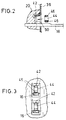
- FIG 2 As shown in Figure 2, provided in the inward side of the housing 20 are depressions 50. The dimensions thereof are practically identical to those of a multi-layer ceramic capacitor 42. Each capacitor is pressed into a depression 50 in the direction of the arrow shown i Figure 2 and then positively held therein.
- Figure 3 shows a region from Figure 1.
- multi-layer ceramic capacitors 44 each bear from above against a plug pin 16, by way of one of their metallized ends 46.
Abstract
Description
- The invention relates to an electrical connector and, in particular to a plug comprising a housing, a ground plate lying on the inside thereof, bores passing through the housing and openings in the ground plate, plug pins which pass through the bores and the openings and which are held in the former, and multi-layer ceramic capacitors which are arranged on the inside of the housing and which are disposed electrically between the ground plate and the plug pins.
- Such plugs are known, one of which is shown, for example, in U.S. 4,930,200, to Brush, et al. Plugs of that kind serve for connecting printed circuit boards to other electrical components. The plug pins thereof are inserted with their one ends into the metallized holes in the printed circuit board. Their other ends extend for example to the wires of a cable. In the transmission of the useful signals from the printed circuit board to the cable, high-frequency signals or interference signals are to be removed. The multi-layer ceramic capacitors which are disposed between a ground plate and the plug pins are provided for that purpose. The capacitors are of dimensions of only a very few millimeters and they are arranged on a printed circuit board which is fixed in the plug. Their metallised ends are soldered to conductor tracks of the circuit board. In many cases, they are additionally glued onto the circuit board. In other words, they are rigidly connected thereto. Accordingly, they follow the movements of the circuit board, even if such movements are slight. The circuit board may be twisted and flexed when it is fitted into the plug housing and when the ground plate is clamped in position. Those movements which may also be imposed on the multi-layer ceramic capacitors which could result in their being damaged. Because the capacitors are made of ceramic material, the multi-layer ceramic capacitors are very brittle. In regard to the known plug, it should be noted that the printed circuit boards represent a particular component and serve only for mechanical and electrical connection of the multi-layer ceramic capacitors.
- Taking that state of the art as its basic starting point, the invention is based on the provision of a plug in which high-frequency interference signals are carried away to ground and the multi-layer ceramic capacitors of which are not subjected to a mechanical loading and which can also be produced cost effectively. The solution to that problem is achieved in a plug of the kind set forth in the opening part of this specification, in accordance with the invention, in that the multi-layer ceramic capacitors are resiliently clamped between the ground plate and the plug pins.
- In accordance with the invention therefore the multi-layer ceramic capacitors are disposed directly between the ground plate and the plug pins and are resiliently clamped between same and are not fitted onto an additional component, such as a printed circuit board. Such arrangement therefore omits the rigid connection to the printed circuit board and the resulting risk of breakage. Finally, the arrangement also omits the printed circuit board itself, as an additional cost-incurring component. The elasticity of the ground plate is considered sufficient to clamp the multi-layer ceramic capacitors in position resiliently and nonetheless securely. The capacitors are sufficiently securely held in place from the mechanical point of view. The pressure applied by the ground plate is also sufficient to provide a sound electrical connection. Nevertheless the manner in which the multi-layer ceramic capacitors are held in position between the plug pins on one side and the ground plate on the other side is not rigid. As such, the multi-layer ceramic capacitors do not follow all possible movements, and as a result they are not subjected to a mechanical loading and the risk of breakage is reduced.
- In order to provide a sufficiently large contact or pressure area as between the multi-layer ceramic capacitors and the ground plate, a desirable configuration provides that the openings in the ground plate are surrounded by plate portions which are bent out of the ground plate towards the housing. The height of such plate portions corresponds at least to the thickness of the multi-layer ceramic capacitors, and the latter are clamped between the plate portions and the plug pins. The plate portions have a flat section extending parallel to the end faces of the multi-layer ceramic capacitors. The length of the plate portions approximately corresponds to the height or thickness of the multi-layer ceramic capacitors. The flat section bears against the end faces or metallized ends of the multi-layer ceramic capacitors.
- So that the ground plate bears in its other regions against the housing of the plug and is not held at a spacing therefrom by its outwardly bent plate portions, a further desirable configuration provides that disposed on the inside of the housing are recesses and the plate portions are bent into said recesses. Furthermore, in another advantageous configuration, a plate lies on the ground plate, the plate having protrusions which are aligned with the openings in the ground plate and the multi-layer ceramic capacitors and bearing against the capacitors. The protrusions of the plate additionally fix the multi-layer ceramic capacitors. Likewise they additionally fix the ground plate.
- The multi-layer ceramic capacitors may be arranged on one or both sides of the plug pins.
- When a multi-layer ceramic capacitor is disposed only on one side of the plug pin, desirably, at the side of the plug pin which is remote from the multi-layer ceramic capacitor, the housing has a support which bears against the plug pin. In addition at the side of the multi-layer ceramic capacitor which is remote from the protrusion of the plate, the housing may have a support which bears against the capacitor. The supports are formed integrally with the housing. The first-mentioned support bears against a plug pin and the additionally mentioned support bears against a multi-layer ceramic capacitor. By virtue of that arrangement those components are additionally supported and fixed in position.
- Depending on the requirements of the respective plug, they may also be soldered with one of their metallized ends to a plug pin and with their other metallized end to the inwardly bent plate portions of the ground plate.
- There are uses in which the plugs are exposed to shocks, shaking movements and/or vibration. For such uses, an embodiment is recommended in accordance with the invention in which depressions are provided on the inside of the housing to receive the multi-layer ceramic capacitors and the latter are disposed in the depressions. The dimensions of the depressions are so matched to those of the multi-layer ceramic capacitors that they are positively held in the depressions.
- The above-described manner of mounting the multi-layer ceramic capacitors in a plug, in accordance with the invention, may also be used in relation to other components. It is also part of the present invention if other components such as inductors, resistors or capacitors of another type are held in the plugs in the described manner.
- The invention will now be further described by way of example by means of the embodiments shown in the drawing in which:
- Figure 1 is a partly sectional side view of a first embodiment of a plug connector.
- Figure 2 is a partly sectional side view of a second embodiment illustrating the depression accommodating a multi-layer ceramic capacitor, and
- Figure 3 is a view taken along line III-III in Figure 1.
- Figure 1 shows a part of a printed
circuit board 12 with metallizedholes 14.Plug pins 16 are fitted into the latter. Some of theplug pins 16 are held together and fixed with aplate portion 18. - Figure 1 shows the
housing 20, insofar as is essential for the present invention. Bores 22 pass through thehousing 20 and accommodate theplug pins 16. Aplate 26 lies on theinside 24 of thehousing 20, with the interposition of the ground plate which is to be described hereinafter. Theplate 26 hasprotrusions 28. Theprotrusions 28 bear against the multi-layer ceramic capacitors which are to be described hereinafter. Figure 1 also showsrivet heads 30 which are formed integrally with thehousing 20. They pass through openings in theplate 26 and fix theplate 26 to thehousing 20. - Figure 1 shows three
plug pins 16. In regard to the two upper plug pins 16, the multi-layer ceramic capacitors to be described hereinafter are disposed only at the top side thereof. In the case of thelower plug pin 16, the multi-layer ceramic capacitors are disposed on both sides thereof. IN the case off the two upper plug pins 16 thehousing 20 hassupports 32 which are formed integrally therewith. The supports 32 engage under and fix the plug pins 16. In that way the pins are protected from being bent. - In the case of all plug pins 16 or multi-layer ceramic capacitors, the housing further has supports or
protuberances 34. The supports 34 are also formed integrally with thehousing 20 and bear against the left-hand side of the multi-layer ceramic capacitors. In that way the capacitors are fixed in a lateral direction between theprotrusions 28 and thesupports 34. - A
ground plate 36 lies on theinward side 24 of thehousing 20. Afront plate 40 is disposed on the other side of thehousing 20. Aground conductor 38 which is connected to theground plate 36 is inserted into ametallised hole 14. Theground plate 36 also bears with resilient ends against the inward side of thefront plate 40. Theground plate 36 has openings surrounding the plug pins 16. The openings haveplate portions 42 which are bent out towards the left, when looking at Figure 1. The plate portions include flat sections which lie against an end of the above-mentioned multi-layerceramic capacitors 44. - As shown in Figure 1, the multi-layer
ceramic capacitors 44 are respectively disposed between aplug pin 16 and aplate portion 42. In that arrangement, a respective multi-layer ceramic capacitor bears against each of the two upper plug pins 16 while two such capacitors bear against thelower plug pin 16. The multi-layerceramic capacitors 44 have metallized ends 46. They can be soldered to the plug pins 16 and the outwardlybent plate portions 42, thereby providingsolder locations 46. - As shown in Figure 2, provided in the inward side of the
housing 20 are depressions 50. The dimensions thereof are practically identical to those of a multi-layerceramic capacitor 42. Each capacitor is pressed into a depression 50 in the direction of the arrow shown i Figure 2 and then positively held therein. Figure 3 shows a region from Figure 1. When looking at the drawing, multi-layerceramic capacitors 44 each bear from above against aplug pin 16, by way of one of their metallized ends 46. - The true scope of the invention is set forth in the claims appended hereto.
Claims (12)
- A filtered plug connector of the type including a housing having a plurality of bores through which a respective plurality of pins pass, a ground plate supported by said housing and a plurality of multi-layer capacitors of the type comprising a pair of spaced external electrodes, one electrode of each capacitor being in engagement with a respective pin and the other electrode of each capacitor being in engagement with the ground plate, characterized in that a plate (26) is supported by and holds said capacitors against said housing in a non-rigid manner, and in that said ground plate (36) comprises a resilient portion (42) projecting outwardly from the ground plate for each capacitor (44), each said resilient portion (42) resiliently engaging one of said capacitor electrodes and pressing said capacitor between said housing (20) and said plate (26) toward said pin (16) to thereby cause engagement of said other capacitor electrode with said pin (16).
- A filtered plug connector as claimed in claim 1, characterized in that said ground plate (36) has a plurality of openings through which said respective plurality of pins extend, said ground plate (36) being interposed between said housing (20) and said plate (26).
- A filtered plug connector as claimed in claim 2, characterized in that said plate (26) is secured to said housing (20).
- A filtered plug connector as claimed in claim 3, characterized in that said pins (16) are generally elongate defining a longitudinal axis, said multi-layer capacitors (44) being of parallelepiped configuration and supported between said housing (20) and said plate (36) in a direction generally transverse to the axis of a respective pin (16), said housing (20) and said plate (36) bearing against each said capacitor (44) on opposite surfaces thereof and substantially preventing movement of each said capacitor (44) in a direction along the pin axis, the resilient portion (42) of the ground plate providing resilient clamping of the capacitor against the pin (16) in a direction transverse to each said pin axis.
- A filtered plug connector as claimed in claim 4, characterized in that said resilient portions 42 are adjacent the respective openings in the ground plate (36) and are bent out of the ground plate (36) towards the housing (20).
- A filtered plug connector as claimed in claim 5, characterized in that recesses are provided on the inside (24) of the housing (20) and the plate portions (42) are bent into said recesses.
- A filtered plug connector as claimed in claim 4, characterized in that said plate (26) has protrusions (28) which are aligned with and extend into the openings in the ground plate (36) and bear against one surface of the multi-layer capacitors (44).
- A filtered plug connector as claimed in claim 7, characterized in that at the surface of the multi-layer ceramic capacitor (44) which is opposite the protrusion (28) of the plate (26), the housing (20) has a support (34) bearing against such surface of the capacitor.
- A filtered plug connector as claimed in claim 4, characterized in that at a side of the plug pin (16) which is remote from the multi-layer ceramic capacitor (44) the housing (20) has a support (32) which bears against such side of the plug pin.
- A filtered connector as claimed in claim 4, characterized in that depressions (50) are provided on the inside (24) of the housing (20) receiving respectively the multi-layer ceramic capacitors (44).
- A filtered plug connector as claimed in claim 1, characterized in that the multi-layer ceramic capacitors (44) are soldered with a metallized electrode (46) to the plug pins (16).
- A filtered plug connector as claimed in claim 11, characterized in that the multi-layer ceramic capacitors (44) are soldered with another metallized electrode (46) to the plate portions (42) of the ground plate (36).
Applications Claiming Priority (2)
| Application Number | Priority Date | Filing Date | Title |
|---|---|---|---|
| DE4037602 | 1990-11-27 | ||
| DE4037602 | 1990-11-27 |
Publications (3)
| Publication Number | Publication Date |
|---|---|
| EP0487984A2 true EP0487984A2 (en) | 1992-06-03 |
| EP0487984A3 EP0487984A3 (en) | 1992-07-22 |
| EP0487984B1 EP0487984B1 (en) | 1995-06-14 |
Family
ID=6418948
Family Applications (1)
| Application Number | Title | Priority Date | Filing Date |
|---|---|---|---|
| EP91119414A Expired - Lifetime EP0487984B1 (en) | 1990-11-27 | 1991-11-14 | Filtered plug connector |
Country Status (6)
| Country | Link |
|---|---|
| US (1) | US5152699A (en) |
| EP (1) | EP0487984B1 (en) |
| JP (1) | JPH0777140B2 (en) |
| AU (1) | AU641061B2 (en) |
| CA (1) | CA2056339C (en) |
| DE (1) | DE69110418T2 (en) |
Cited By (8)
| Publication number | Priority date | Publication date | Assignee | Title |
|---|---|---|---|---|
| WO1994000893A1 (en) * | 1992-06-29 | 1994-01-06 | Siemens Aktiengesellschaft | Filter plug connector with screened casing |
| GB2271676A (en) * | 1992-10-05 | 1994-04-20 | Amphenol Corp | Diode/filter connector |
| GB2273210A (en) * | 1992-12-04 | 1994-06-08 | Fichtel & Sachs Ag | Filtered connector |
| EP0622872A2 (en) * | 1993-04-08 | 1994-11-02 | AMPHENOL-TUCHEL ELECTRONICS GmbH | Circular connector with filter |
| US5417591A (en) * | 1992-12-04 | 1995-05-23 | Fichtel & Sachs Ag | Connection device for an electrical arrangement shielded by an electrically conductive wall of a housing |
| EP0726620A2 (en) * | 1995-02-07 | 1996-08-14 | Johnstech International Corporation | Apparatus for providing controlled impedance in an electrical contact |
| EP0975205A2 (en) * | 1998-07-23 | 2000-01-26 | Delphi Technologies, Inc. | Busplate |
| WO2006076680A1 (en) * | 2005-01-14 | 2006-07-20 | Molex Incorporated | Modular filter connector |
Families Citing this family (26)
| Publication number | Priority date | Publication date | Assignee | Title |
|---|---|---|---|---|
| US5266054A (en) * | 1992-12-22 | 1993-11-30 | The Whitaker Corporation | Sealed and filtered header receptacle |
| US5286224A (en) * | 1993-05-10 | 1994-02-15 | Itt Corporation | Interchangeable contact connector |
| US5340334A (en) * | 1993-07-19 | 1994-08-23 | The Whitaker Corporation | Filtered electrical connector |
| US5399099A (en) * | 1993-08-12 | 1995-03-21 | The Whitaker Corporation | EMI protected tap connector |
| US5599208A (en) * | 1994-12-14 | 1997-02-04 | The Whitaker Corporation | Electrical connector with printed circuit board programmable filter |
| US5562499A (en) * | 1995-01-30 | 1996-10-08 | Stanley E. Gately | Multiposition electrical connector filter adapter |
| US5554050A (en) * | 1995-03-09 | 1996-09-10 | The Whitaker Corporation | Filtering insert for electrical connectors |
| US5580280A (en) * | 1995-06-30 | 1996-12-03 | The Whitaker Corporation | Filtered electrical connector |
| US5624277A (en) * | 1995-08-28 | 1997-04-29 | The Whitaker Corporation | Filtered and shielded electrical connector using resilient electrically conductive member |
| DE19611699C1 (en) * | 1996-03-25 | 1997-11-13 | Siemens Ag | Filter plug connector with screened housing e.g.for automobile air-bag control devices |
| US6033263A (en) * | 1996-10-15 | 2000-03-07 | The Whitaker Corporation | Electrically connector with capacitive coupling |
| US5865648A (en) * | 1997-01-16 | 1999-02-02 | Elco U.S.A. Inc. | Multifunction electronic connector |
| US5975958A (en) * | 1997-10-14 | 1999-11-02 | The Whitaker Corporation | Capactive coupling adapter for an electrical connector |
| US6142831A (en) * | 1999-02-01 | 2000-11-07 | Aux Corporation | Multifunction connector assembly |
| US6858793B1 (en) * | 1999-09-09 | 2005-02-22 | Koninklijke Philips Electronics N.V. | EMI-suppression plate for use in IEEE-1394 applications |
| DE10233318C1 (en) * | 2002-07-22 | 2003-09-25 | Siemens Ag | Interference suppression device for electronic apparatus uses capacitor connected between plug element for apparatus circuit and housing potential |
| JP2004172593A (en) * | 2002-10-23 | 2004-06-17 | Spectrum Control Inc | Dielectric component array |
| US7295086B2 (en) * | 2002-10-23 | 2007-11-13 | Spectrum Control Inc. | Dielectric component array with failsafe link |
| US6837747B1 (en) | 2004-04-19 | 2005-01-04 | Itt Manufacturing Enterprises, Inc. | Filtered connector |
| US7442085B2 (en) * | 2005-01-14 | 2008-10-28 | Molex Incorporated | Filter connector |
| US20090091889A1 (en) * | 2007-10-09 | 2009-04-09 | Oman Todd P | Power electronic module having improved heat dissipation capability |
| ITVI20080063A1 (en) * | 2008-03-12 | 2009-09-13 | Sumoto Srl | POWER CONNECTOR STRUCTURE. |
| US8241067B2 (en) * | 2009-11-04 | 2012-08-14 | Amphenol Corporation | Surface mount footprint in-line capacitance |
| CN102854939B (en) * | 2011-06-30 | 2017-06-06 | 赛恩倍吉科技顾问(深圳)有限公司 | I/O port combinations |
| CN104704682B (en) * | 2012-08-22 | 2017-03-22 | 安费诺有限公司 | High-frequency electrical connector |
| CN105792515A (en) * | 2014-12-25 | 2016-07-20 | 台达电子工业股份有限公司 | Circuit board combination and assembly method thereof |
Citations (2)
| Publication number | Priority date | Publication date | Assignee | Title |
|---|---|---|---|---|
| US4582385A (en) * | 1983-10-31 | 1986-04-15 | International Telephone & Telegraph Corp. | Electrical connector embodying electrical circuit components |
| US4690479A (en) * | 1985-10-10 | 1987-09-01 | Amp Incorporated | Filtered electrical header assembly |
Family Cites Families (7)
| Publication number | Priority date | Publication date | Assignee | Title |
|---|---|---|---|---|
| US4500159A (en) * | 1983-08-31 | 1985-02-19 | Allied Corporation | Filter electrical connector |
| US4707048A (en) * | 1986-11-03 | 1987-11-17 | Amphenol Corporation | Electrical connector having means for protecting terminals from transient voltages |
| JPS63165786U (en) * | 1987-04-16 | 1988-10-28 | ||
| DE8902245U1 (en) * | 1989-02-25 | 1989-05-11 | Thomas & Betts Corp., Bridgewater, N.J., Us | |
| US4950185A (en) * | 1989-05-18 | 1990-08-21 | Amphenol Corporation | Stress isolated planar filter design |
| US4930200A (en) * | 1989-07-28 | 1990-06-05 | Thomas & Betts Corporation | Method of making an electrical filter connector |
| US5057041A (en) * | 1990-06-29 | 1991-10-15 | Foxconn International | User configurable integrated electrical connector assembly |
-
1991
- 1991-11-14 EP EP91119414A patent/EP0487984B1/en not_active Expired - Lifetime
- 1991-11-14 DE DE69110418T patent/DE69110418T2/en not_active Expired - Fee Related
- 1991-11-19 AU AU87959/91A patent/AU641061B2/en not_active Ceased
- 1991-11-21 US US07/796,563 patent/US5152699A/en not_active Expired - Lifetime
- 1991-11-27 CA CA002056339A patent/CA2056339C/en not_active Expired - Fee Related
- 1991-11-27 JP JP3312507A patent/JPH0777140B2/en not_active Expired - Lifetime
Patent Citations (2)
| Publication number | Priority date | Publication date | Assignee | Title |
|---|---|---|---|---|
| US4582385A (en) * | 1983-10-31 | 1986-04-15 | International Telephone & Telegraph Corp. | Electrical connector embodying electrical circuit components |
| US4690479A (en) * | 1985-10-10 | 1987-09-01 | Amp Incorporated | Filtered electrical header assembly |
Cited By (16)
| Publication number | Priority date | Publication date | Assignee | Title |
|---|---|---|---|---|
| WO1994000893A1 (en) * | 1992-06-29 | 1994-01-06 | Siemens Aktiengesellschaft | Filter plug connector with screened casing |
| GB2271676B (en) * | 1992-10-05 | 1997-04-16 | Amphenol Corp | Diode/filter connector |
| GB2271676A (en) * | 1992-10-05 | 1994-04-20 | Amphenol Corp | Diode/filter connector |
| US5498180A (en) * | 1992-10-05 | 1996-03-12 | Amphenol Corporation | Diode/filter connector |
| GB2273210A (en) * | 1992-12-04 | 1994-06-08 | Fichtel & Sachs Ag | Filtered connector |
| FR2699011A1 (en) * | 1992-12-04 | 1994-06-10 | Fichtel & Sachs Ag | Connecting device for electromagnetically insulated electrical apparatus |
| US5417591A (en) * | 1992-12-04 | 1995-05-23 | Fichtel & Sachs Ag | Connection device for an electrical arrangement shielded by an electrically conductive wall of a housing |
| GB2273210B (en) * | 1992-12-04 | 1996-08-07 | Fichtel & Sachs Ag | Connection device for an electrical arrangement shielded by an electrically conductive wall of a housing |
| EP0622872A2 (en) * | 1993-04-08 | 1994-11-02 | AMPHENOL-TUCHEL ELECTRONICS GmbH | Circular connector with filter |
| EP0622872A3 (en) * | 1993-04-08 | 1997-01-22 | Amphenol Tuchel Elect | Circular connector with filter. |
| EP0726620A2 (en) * | 1995-02-07 | 1996-08-14 | Johnstech International Corporation | Apparatus for providing controlled impedance in an electrical contact |
| EP0726620A3 (en) * | 1995-02-07 | 1997-11-05 | Johnstech International Corporation | Apparatus for providing controlled impedance in an electrical contact |
| US5967848A (en) * | 1995-02-07 | 1999-10-19 | Johnstech International Corporation | Apparatus for providing controlled impedance in an electrical contact |
| EP0975205A2 (en) * | 1998-07-23 | 2000-01-26 | Delphi Technologies, Inc. | Busplate |
| EP0975205A3 (en) * | 1998-07-23 | 2000-11-02 | Delphi Technologies, Inc. | Busplate |
| WO2006076680A1 (en) * | 2005-01-14 | 2006-07-20 | Molex Incorporated | Modular filter connector |
Also Published As
| Publication number | Publication date |
|---|---|
| EP0487984B1 (en) | 1995-06-14 |
| CA2056339A1 (en) | 1992-05-28 |
| JPH04267085A (en) | 1992-09-22 |
| AU641061B2 (en) | 1993-09-09 |
| EP0487984A3 (en) | 1992-07-22 |
| AU8795991A (en) | 1992-06-18 |
| CA2056339C (en) | 1995-03-21 |
| US5152699A (en) | 1992-10-06 |
| DE69110418T2 (en) | 1996-03-07 |
| JPH0777140B2 (en) | 1995-08-16 |
| DE69110418D1 (en) | 1995-07-20 |
Similar Documents
| Publication | Publication Date | Title |
|---|---|---|
| US5152699A (en) | Filtered plug connector | |
| KR910001318B1 (en) | Telephone connector | |
| US5239748A (en) | Method of making high density connector for burn-in boards | |
| US5624277A (en) | Filtered and shielded electrical connector using resilient electrically conductive member | |
| JP2801915B2 (en) | Filter unit for connector | |
| US3501582A (en) | Electrical assembly | |
| US5479320A (en) | Board-to-board connector including an insulative spacer having a conducting surface and U-shaped contacts | |
| US4784618A (en) | Filter connector device | |
| US5580280A (en) | Filtered electrical connector | |
| JPH0676894A (en) | Connector | |
| WO1998034296A3 (en) | Multifunction electronic connector | |
| US6743047B2 (en) | Electrical connector with rear ground plate | |
| US6623281B2 (en) | Mounting electronic components on circuit boards | |
| US4629267A (en) | Circuit terminating device | |
| EP0643448B1 (en) | Coaxial connector for connection to a printed circuit board | |
| EP0724312B1 (en) | Multiposition electrical connector filter adapter | |
| JP6734395B2 (en) | Plug connector for data transmission | |
| US6506079B1 (en) | Multi-pole angle-connecting device | |
| US5364293A (en) | Shielded stackable solderless connector/filter assembly | |
| JPH0514469Y2 (en) | ||
| JPH01315212A (en) | Branch connector | |
| EP0569917A1 (en) | Filter connector | |
| JPS5848498A (en) | Electric part unit | |
| US4575165A (en) | Circuit to post interconnection device | |
| JPH08273781A (en) | Chip part packaging socket |
Legal Events
| Date | Code | Title | Description |
|---|---|---|---|
| PUAI | Public reference made under article 153(3) epc to a published international application that has entered the european phase |
Free format text: ORIGINAL CODE: 0009012 |
|
| PUAL | Search report despatched |
Free format text: ORIGINAL CODE: 0009013 |
|
| AK | Designated contracting states |
Kind code of ref document: A2 Designated state(s): BE CH DE ES FR GB IT LI LU NL SE |
|
| AK | Designated contracting states |
Kind code of ref document: A3 Designated state(s): BE CH DE ES FR GB IT LI LU NL SE |
|
| 17P | Request for examination filed |
Effective date: 19930118 |
|
| RAP3 | Party data changed (applicant data changed or rights of an application transferred) |
Owner name: THOMAS & BETTS CORPORATION |
|
| 17Q | First examination report despatched |
Effective date: 19940628 |
|
| GRAA | (expected) grant |
Free format text: ORIGINAL CODE: 0009210 |
|
| AK | Designated contracting states |
Kind code of ref document: B1 Designated state(s): BE CH DE ES FR GB IT LI LU NL SE |
|
| PG25 | Lapsed in a contracting state [announced via postgrant information from national office to epo] |
Ref country code: IT Free format text: LAPSE BECAUSE OF FAILURE TO SUBMIT A TRANSLATION OF THE DESCRIPTION OR TO PAY THE FEE WITHIN THE PRESCRIBED TIME-LIMIT;WARNING: LAPSES OF ITALIAN PATENTS WITH EFFECTIVE DATE BEFORE 2007 MAY HAVE OCCURRED AT ANY TIME BEFORE 2007. THE CORRECT EFFECTIVE DATE MAY BE DIFFERENT FROM THE ONE RECORDED. Effective date: 19950614 Ref country code: LI Effective date: 19950614 Ref country code: BE Effective date: 19950614 Ref country code: ES Free format text: THE PATENT HAS BEEN ANNULLED BY A DECISION OF A NATIONAL AUTHORITY Effective date: 19950614 Ref country code: CH Effective date: 19950614 Ref country code: FR Effective date: 19950614 Ref country code: NL Free format text: LAPSE BECAUSE OF NON-PAYMENT OF DUE FEES Effective date: 19950614 |
|
| REF | Corresponds to: |
Ref document number: 69110418 Country of ref document: DE Date of ref document: 19950720 |
|
| PG25 | Lapsed in a contracting state [announced via postgrant information from national office to epo] |
Ref country code: SE Effective date: 19950914 |
|
| REG | Reference to a national code |
Ref country code: CH Ref legal event code: PL |
|
| EN | Fr: translation not filed | ||
| PG25 | Lapsed in a contracting state [announced via postgrant information from national office to epo] |
Ref country code: LU Free format text: LAPSE BECAUSE OF NON-PAYMENT OF DUE FEES Effective date: 19951130 |
|
| NLV1 | Nl: lapsed or annulled due to failure to fulfill the requirements of art. 29p and 29m of the patents act | ||
| PLBE | No opposition filed within time limit |
Free format text: ORIGINAL CODE: 0009261 |
|
| STAA | Information on the status of an ep patent application or granted ep patent |
Free format text: STATUS: NO OPPOSITION FILED WITHIN TIME LIMIT |
|
| 26N | No opposition filed | ||
| REG | Reference to a national code |
Ref country code: GB Ref legal event code: IF02 |
|
| PGFP | Annual fee paid to national office [announced via postgrant information from national office to epo] |
Ref country code: GB Payment date: 20071128 Year of fee payment: 17 |
|
| PGFP | Annual fee paid to national office [announced via postgrant information from national office to epo] |
Ref country code: DE Payment date: 20071221 Year of fee payment: 17 |
|
| GBPC | Gb: european patent ceased through non-payment of renewal fee |
Effective date: 20081114 |
|
| PG25 | Lapsed in a contracting state [announced via postgrant information from national office to epo] |
Ref country code: DE Free format text: LAPSE BECAUSE OF NON-PAYMENT OF DUE FEES Effective date: 20090603 |
|
| PG25 | Lapsed in a contracting state [announced via postgrant information from national office to epo] |
Ref country code: GB Free format text: LAPSE BECAUSE OF NON-PAYMENT OF DUE FEES Effective date: 20081114 |