EP0488546A1 - Contact for integrated circuits - Google Patents
Contact for integrated circuits Download PDFInfo
- Publication number
- EP0488546A1 EP0488546A1 EP19910310399 EP91310399A EP0488546A1 EP 0488546 A1 EP0488546 A1 EP 0488546A1 EP 19910310399 EP19910310399 EP 19910310399 EP 91310399 A EP91310399 A EP 91310399A EP 0488546 A1 EP0488546 A1 EP 0488546A1
- Authority
- EP
- European Patent Office
- Prior art keywords
- dielectric layer
- layer
- dielectric
- conductor
- integrated circuit
- Prior art date
- Legal status (The legal status is an assumption and is not a legal conclusion. Google has not performed a legal analysis and makes no representation as to the accuracy of the status listed.)
- Withdrawn
Links
Images
Classifications
-
- H—ELECTRICITY
- H01—ELECTRIC ELEMENTS
- H01L—SEMICONDUCTOR DEVICES NOT COVERED BY CLASS H10
- H01L21/00—Processes or apparatus adapted for the manufacture or treatment of semiconductor or solid state devices or of parts thereof
- H01L21/70—Manufacture or treatment of devices consisting of a plurality of solid state components formed in or on a common substrate or of parts thereof; Manufacture of integrated circuit devices or of parts thereof
- H01L21/71—Manufacture of specific parts of devices defined in group H01L21/70
- H01L21/768—Applying interconnections to be used for carrying current between separate components within a device comprising conductors and dielectrics
- H01L21/76801—Applying interconnections to be used for carrying current between separate components within a device comprising conductors and dielectrics characterised by the formation and the after-treatment of the dielectrics, e.g. smoothing
- H01L21/76802—Applying interconnections to be used for carrying current between separate components within a device comprising conductors and dielectrics characterised by the formation and the after-treatment of the dielectrics, e.g. smoothing by forming openings in dielectrics
-
- H—ELECTRICITY
- H01—ELECTRIC ELEMENTS
- H01L—SEMICONDUCTOR DEVICES NOT COVERED BY CLASS H10
- H01L21/00—Processes or apparatus adapted for the manufacture or treatment of semiconductor or solid state devices or of parts thereof
- H01L21/70—Manufacture or treatment of devices consisting of a plurality of solid state components formed in or on a common substrate or of parts thereof; Manufacture of integrated circuit devices or of parts thereof
- H01L21/71—Manufacture of specific parts of devices defined in group H01L21/70
- H01L21/768—Applying interconnections to be used for carrying current between separate components within a device comprising conductors and dielectrics
- H01L21/76801—Applying interconnections to be used for carrying current between separate components within a device comprising conductors and dielectrics characterised by the formation and the after-treatment of the dielectrics, e.g. smoothing
- H01L21/76829—Applying interconnections to be used for carrying current between separate components within a device comprising conductors and dielectrics characterised by the formation and the after-treatment of the dielectrics, e.g. smoothing characterised by the formation of thin functional dielectric layers, e.g. dielectric etch-stop, barrier, capping or liner layers
- H01L21/76831—Applying interconnections to be used for carrying current between separate components within a device comprising conductors and dielectrics characterised by the formation and the after-treatment of the dielectrics, e.g. smoothing characterised by the formation of thin functional dielectric layers, e.g. dielectric etch-stop, barrier, capping or liner layers in via holes or trenches, e.g. non-conductive sidewall liners
-
- H—ELECTRICITY
- H01—ELECTRIC ELEMENTS
- H01L—SEMICONDUCTOR DEVICES NOT COVERED BY CLASS H10
- H01L23/00—Details of semiconductor or other solid state devices
- H01L23/52—Arrangements for conducting electric current within the device in operation from one component to another, i.e. interconnections, e.g. wires, lead frames
- H01L23/522—Arrangements for conducting electric current within the device in operation from one component to another, i.e. interconnections, e.g. wires, lead frames including external interconnections consisting of a multilayer structure of conductive and insulating layers inseparably formed on the semiconductor body
- H01L23/532—Arrangements for conducting electric current within the device in operation from one component to another, i.e. interconnections, e.g. wires, lead frames including external interconnections consisting of a multilayer structure of conductive and insulating layers inseparably formed on the semiconductor body characterised by the materials
- H01L23/5329—Insulating materials
-
- H—ELECTRICITY
- H01—ELECTRIC ELEMENTS
- H01L—SEMICONDUCTOR DEVICES NOT COVERED BY CLASS H10
- H01L2924/00—Indexing scheme for arrangements or methods for connecting or disconnecting semiconductor or solid-state bodies as covered by H01L24/00
- H01L2924/0001—Technical content checked by a classifier
- H01L2924/0002—Not covered by any one of groups H01L24/00, H01L24/00 and H01L2224/00
Definitions
- the present invention relates generally to semiconductor integrated circuits, and more specifically to formation of a contact structure for such circuits.
- One type of structure commonly found on a semiconductor integrated circuit is a contact from an upper level metal interconnect layer to a lower conductive structure through a contact via.
- An interlevel dielectric through which the contact via is cut often has a reflow glass layer to improve planarity of the chip's surface.
- This glass layer typically has impurities which can migrate into the metal interconnect in the via and adversely affect its operation. For example, it is known that mobile ion donation from glass layers in contact with metal interconnect can shift data retention voltages in memory circuits. Also, outgassing of solvents in such a glass layer can cause voiding in, or oxidation of, sputtered metal interconnect.
- a method for forming a contact in a semiconductor integrated circuit includes the formation of a conformal oxide layer over the device followed by formation of a doped glass layer.
- the integrated circuit is heated to cause the glass layer to reflow, improving planarity of the circuit.
- a second conformal oxide layer is then formed, and contact vias are cut through the three part interlevel dielectric layer. Side walls are then formed in the via by depositing a third conformal layer, and anisotropically etching such layer. This isolates the doped reflowable glass layer from the via.
- Metal interconnect can then be deposited and defined, forming a contact in the via.
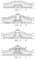
- Figures 1-4 illustrate a preferred method for forming a contact through an interlevel dielectric layer according to the present invention.
- a contact is to be formed on a semiconductor substrate 10 .
- Substrate 10 may be simply the substrate on which an integrated circuit is formed, or it may represent multiple lower layers which have already been fabricated. The details of any such multiple lower layers are not important to the present invention.
- Interconnect 12 is defined and patterned on the substrate 10 .
- Interconnect 12 may be a first metal level interconnect layer, or it may be polycrystalline silicon or a silicided polycrystalline silicon layer.
- a conformal dielectric layer 14 is deposited over the surface of the integrated circuit, followed by a reflowable glass layer 16 .
- Dielectric layer 14 is preferably an oxide layer, undoped or lightly doped as known in the art.
- Layer 14 is typically deposited using chemical vapor deposition (CVD) or low pressure chemical vapor deposition (LPCVD).
- reflowable glass layer 16 is typically amorphous silicon dioxide doped with impurities such as boron, to form boron doped silicate glass (BSG), or boron and phosphorus to form borophoso-silicate glass (BPSG).
- BSG boron doped silicate glass
- BPSG borophoso-silicate glass
- the integrated circuit is heated to cause the glass layer 16 to soften and partially flow into lower topographical regions on the integrated circuit. This heating is generally referred to as reflow. Heating may be performed by inserting the integrated circuit into a furnace, or through rapid thermal processing (RTP) as known in the art. Reflowing of glass layer 16 increases the planarity of its upper surface.
- RTP rapid thermal processing
- Another conformal dielectric layer 18 is then deposited over the glass layer 16 .
- Layer 18 is preferably a CVD or LPCVD oxide layer which is undoped or lightly doped.
- the three layers 14 , 16 , 18 together form an interlevel di
- a photomasking pattern (not shown) is used to define and etch contact via 20 .
- Via 20 provides an opening through the dielectric layers 14 , 16 , 18 to the interconnect layer 12 beneath.
- a conformal dielectric layer 22 is then deposited over the integrated circuit. This layer is also preferably an undoped oxide layer deposited using CVD or LPCVD techniques.
- the dielectric layer 22 is anisotropically etched to remove it from the horizontal surfaces of the integrated circuit. This leaves behind sidewall spacer structures 24 along the sidewalls of the contact via 20 .
- the anisotropic etch used to form spacers 24 will also typically remove a portion of dielectric layer 18 . Since over etching must be performed to ensure clearance of all oxide from the bottom of the contact via 20 , layer 18 is preferably thick enough to ensure that the reflowable glass layer 16 is not exposed by such over etch.
- the reflowable glass 16 is completely isolated from the contact via 20 by the sidewall spacers 24 . Since dielectric layer 18 was initially deposited with enough thickness to ensure that at least part of such layer remains after the anisotropic etch step, metal or other interconnect lying above the interlevel dielectric layer does not make contact with the glass layer 16 .
- interconnect layer 26 is deposited and patterned.
- Layer 26 can be a metal layer, such as aluminum, and can include a layer of refractory metal (not shown) beneath it as known in the art.
- Layer 26 could also be a polycrystalline silicon or silicided polycrystalline silicon layer as known in the art.
- interconnect layer 26 is separated from the reflow glass layer 16 by sidewall spacers 24 and dielectric layer 18 . This protects interconnect layer 26 from impurities contained within the reflow glass layer 16 .
- the method described above, and the structure formed thereby provides for isolation of an interconnect layer and contact from a reflow glass layer used for planarization of an integrated circuit.
- Formation of the upper layer 18 and sidewall spacers 24 adds a minimal amount of complexity to the process flow, and is compatible with standard process flows currently in use. This technique allows for improved contact formation while retaining the advantages of using a reflow glass for planarization.
Abstract
Description
- The present invention relates generally to semiconductor integrated circuits, and more specifically to formation of a contact structure for such circuits.
- In fabricating semiconductor integrated circuits, the integrity of various structures on the circuit is of great importance. Undesirable impurities in the wrong portions of a circuit can adversely affect its functioning.
- One type of structure commonly found on a semiconductor integrated circuit is a contact from an upper level metal interconnect layer to a lower conductive structure through a contact via. An interlevel dielectric through which the contact via is cut often has a reflow glass layer to improve planarity of the chip's surface. This glass layer typically has impurities which can migrate into the metal interconnect in the via and adversely affect its operation. For example, it is known that mobile ion donation from glass layers in contact with metal interconnect can shift data retention voltages in memory circuits. Also, outgassing of solvents in such a glass layer can cause voiding in, or oxidation of, sputtered metal interconnect.
- Since the formation of a reflowable glass layer improves the planarity of the integrated circuit, it is important to use such material in interlevel dielectric layers. It would be desirable to provide a technique which allows the planarity improvement of a reflowable glass without contamination of interconnect by the impurities used in standard glasses.
- It is therefore an object of the present invention to provide a method and structure for use in semiconductor integrated circuits which prevents contamination of metal interconnects and contacts by impurities in an interlevel dielectric layer.
- It is another object of the present invention to provide such a method and structure which allows use of commonly available reflowable glasses to improve planarity of the integrated circuit.
- It is a further object of the present invention to provide such a method and structure which is compatible with standard process flows, and which adds minimal additional complexity to the fabrication of a typical integrated circuit.
- Therefore, according to the present invention, a method for forming a contact in a semiconductor integrated circuit includes the formation of a conformal oxide layer over the device followed by formation of a doped glass layer. The integrated circuit is heated to cause the glass layer to reflow, improving planarity of the circuit. A second conformal oxide layer is then formed, and contact vias are cut through the three part interlevel dielectric layer. Side walls are then formed in the via by depositing a third conformal layer, and anisotropically etching such layer. This isolates the doped reflowable glass layer from the via. Metal interconnect can then be deposited and defined, forming a contact in the via.
- The novel features believed characteristic of the invention are set forth in the appended claims. The invention itself however, as well as a preferred mode of use, and further objects and advantages thereof, will best be understood by reference to the following detailed description of an illustrative embodiment when read in conjunction with the accompanying drawings, wherein:
- Figures 1-4 illustrate a preferred method for forming a contact through an interlevel dielectric layer according to the present invention.
- The process steps and structures described below do not form a complete process flow for manufacturing integrated circuits. The present invention can be practiced in conjunction with integrated circuit fabrication techniques currently used in the art, and only so much of the commonly practiced process steps are included as are necessary for an understanding of the present invention. The figures representing cross-sections of portions of an integrated circuit during fabrication are not drawn to scale, but instead are drawn so as to illustrate the important features of the invention.
- Referring to Figure 1, a contact is to be formed on a
semiconductor substrate 10.Substrate 10 may be simply the substrate on which an integrated circuit is formed, or it may represent multiple lower layers which have already been fabricated. The details of any such multiple lower layers are not important to the present invention. - An
interconnect lead 12 is defined and patterned on thesubstrate 10. Interconnect 12 may be a first metal level interconnect layer, or it may be polycrystalline silicon or a silicided polycrystalline silicon layer. A conformaldielectric layer 14 is deposited over the surface of the integrated circuit, followed by areflowable glass layer 16.Dielectric layer 14 is preferably an oxide layer, undoped or lightly doped as known in the art.Layer 14 is typically deposited using chemical vapor deposition (CVD) or low pressure chemical vapor deposition (LPCVD). - As known in the art,
reflowable glass layer 16 is typically amorphous silicon dioxide doped with impurities such as boron, to form boron doped silicate glass (BSG), or boron and phosphorus to form borophoso-silicate glass (BPSG). Onceglass layer 16 has been deposited, the integrated circuit is heated to cause theglass layer 16 to soften and partially flow into lower topographical regions on the integrated circuit. This heating is generally referred to as reflow. Heating may be performed by inserting the integrated circuit into a furnace, or through rapid thermal processing (RTP) as known in the art. Reflowing ofglass layer 16 increases the planarity of its upper surface. Another conformaldielectric layer 18 is then deposited over theglass layer 16.Layer 18 is preferably a CVD or LPCVD oxide layer which is undoped or lightly doped. The threelayers - Referring to Figure 2, a photomasking pattern (not shown) is used to define and etch contact via 20.
Via 20 provides an opening through thedielectric layers interconnect layer 12 beneath. A conformaldielectric layer 22 is then deposited over the integrated circuit. This layer is also preferably an undoped oxide layer deposited using CVD or LPCVD techniques. - Referring to Figure 3, the
dielectric layer 22 is anisotropically etched to remove it from the horizontal surfaces of the integrated circuit. This leaves behindsidewall spacer structures 24 along the sidewalls of the contact via 20. The anisotropic etch used to formspacers 24 will also typically remove a portion ofdielectric layer 18. Since over etching must be performed to ensure clearance of all oxide from the bottom of the contact via 20,layer 18 is preferably thick enough to ensure that thereflowable glass layer 16 is not exposed by such over etch. - As shown in Figure 3, the
reflowable glass 16 is completely isolated from the contact via 20 by thesidewall spacers 24. Sincedielectric layer 18 was initially deposited with enough thickness to ensure that at least part of such layer remains after the anisotropic etch step, metal or other interconnect lying above the interlevel dielectric layer does not make contact with theglass layer 16. - Referring to Figure 4,
interconnect layer 26 is deposited and patterned.Layer 26 can be a metal layer, such as aluminum, and can include a layer of refractory metal (not shown) beneath it as known in the art.Layer 26 could also be a polycrystalline silicon or silicided polycrystalline silicon layer as known in the art. As described above,interconnect layer 26 is separated from thereflow glass layer 16 bysidewall spacers 24 anddielectric layer 18. This protectsinterconnect layer 26 from impurities contained within thereflow glass layer 16. - As will be appreciated by those skilled in the art, the method described above, and the structure formed thereby, provides for isolation of an interconnect layer and contact from a reflow glass layer used for planarization of an integrated circuit. Formation of the
upper layer 18 andsidewall spacers 24 adds a minimal amount of complexity to the process flow, and is compatible with standard process flows currently in use. This technique allows for improved contact formation while retaining the advantages of using a reflow glass for planarization. - While the invention has been particularly shown and described with reference to a preferred embodiment, it will be understood by those skilled in the art that various changes in form and detail may be made therein without departing from the spirit and scope of the invention.
Claims (17)
- A contact structure for an integrated circuit, comprising:
a first conductor on a semiconductor substrate;
a first dielectric layer overlying said conductor and the substrate;
a second dielectric layer overlying said first dielectric layer;
a third dielectric layer overlying said second dielectric layer;
an opening through said first, second, and third dielectric layers to expose a portion of said first conductor;
sidewall dielectric spacers along sides of said opening; and
a second conductor overlying portions of said third dielectric layer and extending into said opening; wherein said second conductor makes electrical contact with said first conductor and is separated from said second insulating layer by said sidewall spacers and said third dielectric layer. - The contact structure of Claim 1, wherein said second dielectric layer comprises a reflowable glass.
- The contact structure of claim 1, wherein said first conductor comprises a conductive metal.
- The contact structure of claim 1 wherein said first conductor comprises polycrystalline silicon.
- The contact structure of claim 4, wherein said polycrystalline silicon is silicided with a refractory metal.
- The contact structure of claim 1, wherein said second conductor comprises a conductive metal.
- The contact structure of claim 1, wherein said first and third dielectric layers are conformal with their respective underlying structures.
- An interlevel dielectric structure for an integrated circuit, comprising:
a first dielectric layer of oxide;
a second dielectric layer of oxide containing a doping impurity overlying said first oxide layer;
a third dielectric layer of oxide overlying said second oxide layer;
a plurality of openings through said first, second, and third dielectric layers; and
sidewall oxide spacers in said openings, wherein said second dielectric layer is completely surrounded by said first and third dielectric layers and said sidewall spacers. - The structure of claim 2 or claim 8 wherein the second dielectric layer doping impurity comprises boron.
- The structure of claim 2 or claim 8, wherein the second dielectric layer doping impurity comprises phosphorous.
- The structure or claim 1 or claim 8, wherein said second dielectric layer comprises spin-on glass.
- The structure of claim 1 or claim 8, wherein said first and third dielectric layers, are substantially undoped.
- The structure of claim 12 wherein said sidewall spacers are substantially undoped.
- The structure of claim 2 or claim 8, wherein said second dielectric layer has an upper surface which is more nearly planar than said first dielectric layer.
- A method for forming an integrated circuit contact structure, comprising the steps of:
forming a first dielectric layer over a semiconductor substrate;
forming a second dielectric layer over the first dielectric layer;
heating the integrated circuit to soften the second dielectric layer, wherein the second dielectric layer partially flows into lower topographic regions of the integrated circuit, whereby an upper surface of the second dielectric layer is more nearly planar than the first dielectric layer;
forming a third dielectric layer over the second dielectric layer;
forming an opening through the first, second, and third dielectric layers to a conductive region in the substrate;
forming sidewall dielectric regions in the opening, wherein the second dielectric layer is separated from the opening thereby; and
forming a conductor over portions of the third dielectric layer and extending into the opening of make contact with the conductive region. - The method of claim 15, wherein the second dielectric layer is formed from a glass containing boron or phosphorous.
- The method of claim 15, wherein the second dielectric layer comprises spin-on glass.
Applications Claiming Priority (2)
| Application Number | Priority Date | Filing Date | Title |
|---|---|---|---|
| US07/614,296 US5117273A (en) | 1990-11-16 | 1990-11-16 | Contact for integrated circuits |
| US614296 | 1990-11-16 |
Publications (1)
| Publication Number | Publication Date |
|---|---|
| EP0488546A1 true EP0488546A1 (en) | 1992-06-03 |
Family
ID=24460639
Family Applications (1)
| Application Number | Title | Priority Date | Filing Date |
|---|---|---|---|
| EP19910310399 Withdrawn EP0488546A1 (en) | 1990-11-16 | 1991-11-11 | Contact for integrated circuits |
Country Status (3)
| Country | Link |
|---|---|
| US (1) | US5117273A (en) |
| EP (1) | EP0488546A1 (en) |
| JP (1) | JPH04286330A (en) |
Cited By (5)
| Publication number | Priority date | Publication date | Assignee | Title |
|---|---|---|---|---|
| EP0558260A1 (en) * | 1992-02-28 | 1993-09-01 | STMicroelectronics, Inc. | Method for formation of contact vias in integrated circuits |
| EP0892428A2 (en) * | 1997-07-17 | 1999-01-20 | Sharp Kabushiki Kaisha | Method of producing low resistance contacts between integrated circuit metal levels and structure produced thereby. |
| EP0660393B1 (en) * | 1993-12-23 | 2000-05-10 | STMicroelectronics, Inc. | Method and dielectric structure for facilitating overetching of metal without damage to inter-level dielectric |
| US6140222A (en) * | 1992-09-22 | 2000-10-31 | Lucent Technologies Inc. | Integrated circuit dielectric formation |
| EP0706211B1 (en) * | 1994-10-05 | 2004-12-01 | Micronas GmbH | Connection structure for bilayers |
Families Citing this family (26)
| Publication number | Priority date | Publication date | Assignee | Title |
|---|---|---|---|---|
| JP2669153B2 (en) * | 1990-12-19 | 1997-10-27 | 日本電気株式会社 | Method for manufacturing semiconductor device |
| EP0499433B1 (en) * | 1991-02-12 | 1998-04-15 | Matsushita Electronics Corporation | Semiconductor device with improved reliability wiring and method of its fabrication |
| US5294295A (en) * | 1991-10-31 | 1994-03-15 | Vlsi Technology, Inc. | Method for moisture sealing integrated circuits using silicon nitride spacer protection of oxide passivation edges |
| US5424570A (en) * | 1992-01-31 | 1995-06-13 | Sgs-Thomson Microelectronics, Inc. | Contact structure for improving photoresist adhesion on a dielectric layer |
| US5321211A (en) * | 1992-04-30 | 1994-06-14 | Sgs-Thomson Microelectronics, Inc. | Integrated circuit via structure |
| US5317192A (en) * | 1992-05-06 | 1994-05-31 | Sgs-Thomson Microelectronics, Inc. | Semiconductor contact via structure having amorphous silicon side walls |
| KR960002073B1 (en) * | 1992-06-10 | 1996-02-10 | 삼성전자주식회사 | Fabricating method of semiconductor device |
| US5825078A (en) * | 1992-09-23 | 1998-10-20 | Dow Corning Corporation | Hermetic protection for integrated circuits |
| JP3271094B2 (en) * | 1993-07-05 | 2002-04-02 | ソニー株式会社 | Laminated wiring board and method of manufacturing the same |
| US5435888A (en) * | 1993-12-06 | 1995-07-25 | Sgs-Thomson Microelectronics, Inc. | Enhanced planarization technique for an integrated circuit |
| US6284584B1 (en) | 1993-12-17 | 2001-09-04 | Stmicroelectronics, Inc. | Method of masking for periphery salicidation of active regions |
| US5439846A (en) * | 1993-12-17 | 1995-08-08 | Sgs-Thomson Microelectronics, Inc. | Self-aligned method for forming contact with zero offset to gate |
| US6107194A (en) * | 1993-12-17 | 2000-08-22 | Stmicroelectronics, Inc. | Method of fabricating an integrated circuit |
| US5756397A (en) * | 1993-12-28 | 1998-05-26 | Lg Semicon Co., Ltd. | Method of fabricating a wiring in a semiconductor device |
| US6040020A (en) | 1995-08-07 | 2000-03-21 | Micron Technology, Inc. | Method of forming a film having enhanced reflow characteristics at low thermal budget |
| JPH10509285A (en) * | 1995-09-14 | 1998-09-08 | アドバンスト・マイクロ・ディバイシズ・インコーポレイテッド | Damask process for reduced feature size |
| US6130482A (en) * | 1995-09-26 | 2000-10-10 | Fujitsu Limited | Semiconductor device and method for fabricating the same |
| US5675185A (en) * | 1995-09-29 | 1997-10-07 | International Business Machines Corporation | Semiconductor structure incorporating thin film transistors with undoped cap oxide layers |
| JPH09116009A (en) * | 1995-10-23 | 1997-05-02 | Sony Corp | Forming method for connecting hole |
| US5683930A (en) * | 1995-12-06 | 1997-11-04 | Micron Technology Inc. | SRAM cell employing substantially vertically elongated pull-up resistors and methods of making, and resistor constructions and methods of making |
| US5847460A (en) * | 1995-12-19 | 1998-12-08 | Stmicroelectronics, Inc. | Submicron contacts and vias in an integrated circuit |
| US6111319A (en) | 1995-12-19 | 2000-08-29 | Stmicroelectronics, Inc. | Method of forming submicron contacts and vias in an integrated circuit |
| JP2809183B2 (en) * | 1996-03-27 | 1998-10-08 | 日本電気株式会社 | Method for manufacturing semiconductor memory device |
| US5913150A (en) * | 1997-04-11 | 1999-06-15 | Nec Corporation | Method for manufacturing semiconductor device using spin on glass layer |
| US5960315A (en) * | 1997-07-10 | 1999-09-28 | International Business Machines Corporation | Tapered via using sidewall spacer reflow |
| US6080672A (en) * | 1997-08-20 | 2000-06-27 | Micron Technology, Inc. | Self-aligned contact formation for semiconductor devices |
Citations (2)
| Publication number | Priority date | Publication date | Assignee | Title |
|---|---|---|---|---|
| US4489481A (en) * | 1982-09-20 | 1984-12-25 | Texas Instruments Incorporated | Insulator and metallization method for VLSI devices with anisotropically-etched contact holes |
| EP0398834A2 (en) * | 1989-05-15 | 1990-11-22 | International Business Machines Corporation | Method of forming contacts to a semiconductor device |
Family Cites Families (3)
| Publication number | Priority date | Publication date | Assignee | Title |
|---|---|---|---|---|
| JPS54149469A (en) * | 1978-05-16 | 1979-11-22 | Toshiba Corp | Semiconductor device |
| US4972251A (en) * | 1985-08-14 | 1990-11-20 | Fairchild Camera And Instrument Corp. | Multilayer glass passivation structure and method for forming the same |
| US4962414A (en) * | 1988-02-11 | 1990-10-09 | Sgs-Thomson Microelectronics, Inc. | Method for forming a contact VIA |
-
1990
- 1990-11-16 US US07/614,296 patent/US5117273A/en not_active Expired - Lifetime
-
1991
- 1991-11-11 EP EP19910310399 patent/EP0488546A1/en not_active Withdrawn
- 1991-11-14 JP JP3299230A patent/JPH04286330A/en active Pending
Patent Citations (2)
| Publication number | Priority date | Publication date | Assignee | Title |
|---|---|---|---|---|
| US4489481A (en) * | 1982-09-20 | 1984-12-25 | Texas Instruments Incorporated | Insulator and metallization method for VLSI devices with anisotropically-etched contact holes |
| EP0398834A2 (en) * | 1989-05-15 | 1990-11-22 | International Business Machines Corporation | Method of forming contacts to a semiconductor device |
Non-Patent Citations (3)
| Title |
|---|
| IBM TECHNICAL DISCLOSURE BULLETIN. vol. 30, no. 8, January 1988, NEW YORK US pages 295 - 296; ANONYMOUS: 'Nitride sidewall apscers used as a contamination barrier' * |
| IBM TECHNICAL DISCLOSURE BULLETIN. vol. 32, no. 10B, March 1990, NEW YORK US pages 114 - 115; ANONYMOUS: 'Lithographic patterns with a barrier liner' * |
| PHILIPS JOURNAL OF RESEARCH. vol. 44, no. 2-3, 28 July 1989, EINDHOVEN NL pages 257 - 293; OSINSKI ET AL: 'A 0.1 um process for logic applications' * |
Cited By (8)
| Publication number | Priority date | Publication date | Assignee | Title |
|---|---|---|---|---|
| EP0558260A1 (en) * | 1992-02-28 | 1993-09-01 | STMicroelectronics, Inc. | Method for formation of contact vias in integrated circuits |
| US5384483A (en) * | 1992-02-28 | 1995-01-24 | Sgs-Thomson Microelectronics, Inc. | Planarizing glass layer spaced from via holes |
| US5437763A (en) * | 1992-02-28 | 1995-08-01 | Sgs-Thomson Microelectronics, Inc. | Method for formation of contact vias in integrated circuits |
| US6140222A (en) * | 1992-09-22 | 2000-10-31 | Lucent Technologies Inc. | Integrated circuit dielectric formation |
| EP0660393B1 (en) * | 1993-12-23 | 2000-05-10 | STMicroelectronics, Inc. | Method and dielectric structure for facilitating overetching of metal without damage to inter-level dielectric |
| EP0706211B1 (en) * | 1994-10-05 | 2004-12-01 | Micronas GmbH | Connection structure for bilayers |
| EP0892428A2 (en) * | 1997-07-17 | 1999-01-20 | Sharp Kabushiki Kaisha | Method of producing low resistance contacts between integrated circuit metal levels and structure produced thereby. |
| EP0892428A3 (en) * | 1997-07-17 | 1999-11-24 | Sharp Kabushiki Kaisha | Method of producing low resistance contacts between integrated circuit metal levels and structure produced thereby. |
Also Published As
| Publication number | Publication date |
|---|---|
| US5117273A (en) | 1992-05-26 |
| JPH04286330A (en) | 1992-10-12 |
Similar Documents
| Publication | Publication Date | Title |
|---|---|---|
| US5117273A (en) | Contact for integrated circuits | |
| US5444019A (en) | Semiconductor contact via structure and method | |
| US6476488B1 (en) | Method for fabricating borderless and self-aligned polysilicon and metal contact landing plugs for multilevel interconnections | |
| EP0542477B1 (en) | Method of forming an integrated circuit with self-aligned contact between closely spaced features | |
| US6285073B1 (en) | Contact structure and method of formation | |
| EP0435388B1 (en) | Method for selectively filling contacts or vias of various depths | |
| US5668052A (en) | Method of manufacturing semiconductor device | |
| KR910006370B1 (en) | Method of forming holes in semiconductor intergrated circuit device | |
| US20090004809A1 (en) | Method of Integration of a MIM Capacitor with a Lower Plate of Metal Gate Material Formed on an STI Region or a Silicide Region Formed in or on the Surface of a Doped Well with a High K Dielectric Material | |
| US6001726A (en) | Method for using a conductive tungsten nitride etch stop layer to form conductive interconnects and tungsten nitride contact structure | |
| EP0236123A2 (en) | A semiconductor device and method for preparing the same | |
| JPH08102449A (en) | Self-conformity contact using organic containing permittivity material | |
| US5234852A (en) | Sloped spacer for MOS field effect devices comprising reflowable glass layer | |
| JP2000082682A (en) | Fabrication of semiconductor-insulation layer and element having it | |
| JPS63313837A (en) | Device for interconnecting between buried multiple levels | |
| US4933297A (en) | Method for etching windows having different depths | |
| US20020130347A1 (en) | Formation of a frontside contact on silicon-on-insulator substrate | |
| JP2720796B2 (en) | Method for manufacturing semiconductor device | |
| US6551901B1 (en) | Method for preventing borderless contact to well leakage | |
| US6613672B1 (en) | Apparatus and process of fabricating a trench capacitor | |
| US5994228A (en) | Method of fabricating contact holes in high density integrated circuits using taper contact and self-aligned etching processes | |
| EP0520658B1 (en) | Structure and method for contacts in CMOS devices | |
| US6316816B1 (en) | Film resistor and method of producing same | |
| EP0566253A1 (en) | Method for forming contact structures in integrated circuits | |
| EP0164186A1 (en) | Method of manufacturing CMOS devices |
Legal Events
| Date | Code | Title | Description |
|---|---|---|---|
| PUAI | Public reference made under article 153(3) epc to a published international application that has entered the european phase |
Free format text: ORIGINAL CODE: 0009012 |
|
| AK | Designated contracting states |
Kind code of ref document: A1 Designated state(s): DE FR GB IT |
|
| RIN1 | Information on inventor provided before grant (corrected) |
Inventor name: CLARK, WAYNE DAVID Inventor name: STARK, DAVID MICHAEL |
|
| 17P | Request for examination filed |
Effective date: 19921126 |
|
| 17Q | First examination report despatched |
Effective date: 19971029 |
|
| RAP3 | Party data changed (applicant data changed or rights of an application transferred) |
Owner name: STMICROELECTRONICS, INC. |
|
| STAA | Information on the status of an ep patent application or granted ep patent |
Free format text: STATUS: THE APPLICATION IS DEEMED TO BE WITHDRAWN |
|
| 18D | Application deemed to be withdrawn |
Effective date: 19990601 |