EP0495571A2 - Universal electronic ballast system - Google Patents
Universal electronic ballast system Download PDFInfo
- Publication number
- EP0495571A2 EP0495571A2 EP92300091A EP92300091A EP0495571A2 EP 0495571 A2 EP0495571 A2 EP 0495571A2 EP 92300091 A EP92300091 A EP 92300091A EP 92300091 A EP92300091 A EP 92300091A EP 0495571 A2 EP0495571 A2 EP 0495571A2
- Authority
- EP
- European Patent Office
- Prior art keywords
- coupled
- transistor
- switching
- voltage
- responsive
- Prior art date
- Legal status (The legal status is an assumption and is not a legal conclusion. Google has not performed a legal analysis and makes no representation as to the accuracy of the status listed.)
- Granted
Links
- 238000004804 winding Methods 0.000 claims abstract description 101
- 230000001105 regulatory effect Effects 0.000 claims abstract description 56
- 230000008878 coupling Effects 0.000 claims abstract description 28
- 238000010168 coupling process Methods 0.000 claims abstract description 28
- 238000005859 coupling reaction Methods 0.000 claims abstract description 28
- 230000006698 induction Effects 0.000 claims abstract description 18
- 230000008859 change Effects 0.000 claims description 9
- 230000033228 biological regulation Effects 0.000 claims description 7
- 230000001939 inductive effect Effects 0.000 claims description 5
- 230000001419 dependent effect Effects 0.000 claims 2
- 230000005291 magnetic effect Effects 0.000 abstract description 9
- 239000003990 capacitor Substances 0.000 description 46
- 230000001052 transient effect Effects 0.000 description 6
- 238000010586 diagram Methods 0.000 description 5
- 230000010355 oscillation Effects 0.000 description 4
- 230000003252 repetitive effect Effects 0.000 description 4
- 238000013459 approach Methods 0.000 description 3
- 238000012544 monitoring process Methods 0.000 description 3
- 239000004065 semiconductor Substances 0.000 description 3
- 238000001914 filtration Methods 0.000 description 2
- 229910044991 metal oxide Inorganic materials 0.000 description 2
- 150000004706 metal oxides Chemical class 0.000 description 2
- 230000002441 reversible effect Effects 0.000 description 2
- 230000009471 action Effects 0.000 description 1
- 239000000654 additive Substances 0.000 description 1
- 230000000996 additive effect Effects 0.000 description 1
- 230000015556 catabolic process Effects 0.000 description 1
- 230000001276 controlling effect Effects 0.000 description 1
- 230000002939 deleterious effect Effects 0.000 description 1
- 238000001514 detection method Methods 0.000 description 1
- 230000005669 field effect Effects 0.000 description 1
- 238000009730 filament winding Methods 0.000 description 1
- 238000009499 grossing Methods 0.000 description 1
- 230000006872 improvement Effects 0.000 description 1
- 230000000977 initiatory effect Effects 0.000 description 1
- 230000002452 interceptive effect Effects 0.000 description 1
- 238000004519 manufacturing process Methods 0.000 description 1
- 230000004048 modification Effects 0.000 description 1
- 238000012986 modification Methods 0.000 description 1
- 230000002093 peripheral effect Effects 0.000 description 1
- 230000001681 protective effect Effects 0.000 description 1
Images


Classifications
-
- H—ELECTRICITY
- H05—ELECTRIC TECHNIQUES NOT OTHERWISE PROVIDED FOR
- H05B—ELECTRIC HEATING; ELECTRIC LIGHT SOURCES NOT OTHERWISE PROVIDED FOR; CIRCUIT ARRANGEMENTS FOR ELECTRIC LIGHT SOURCES, IN GENERAL
- H05B41/00—Circuit arrangements or apparatus for igniting or operating discharge lamps
- H05B41/14—Circuit arrangements
- H05B41/26—Circuit arrangements in which the lamp is fed by power derived from dc by means of a converter, e.g. by high-voltage dc
- H05B41/28—Circuit arrangements in which the lamp is fed by power derived from dc by means of a converter, e.g. by high-voltage dc using static converters
-
- H—ELECTRICITY
- H05—ELECTRIC TECHNIQUES NOT OTHERWISE PROVIDED FOR
- H05B—ELECTRIC HEATING; ELECTRIC LIGHT SOURCES NOT OTHERWISE PROVIDED FOR; CIRCUIT ARRANGEMENTS FOR ELECTRIC LIGHT SOURCES, IN GENERAL
- H05B41/00—Circuit arrangements or apparatus for igniting or operating discharge lamps
- H05B41/14—Circuit arrangements
-
- Y—GENERAL TAGGING OF NEW TECHNOLOGICAL DEVELOPMENTS; GENERAL TAGGING OF CROSS-SECTIONAL TECHNOLOGIES SPANNING OVER SEVERAL SECTIONS OF THE IPC; TECHNICAL SUBJECTS COVERED BY FORMER USPC CROSS-REFERENCE ART COLLECTIONS [XRACs] AND DIGESTS
- Y10—TECHNICAL SUBJECTS COVERED BY FORMER USPC
- Y10S—TECHNICAL SUBJECTS COVERED BY FORMER USPC CROSS-REFERENCE ART COLLECTIONS [XRACs] AND DIGESTS
- Y10S315/00—Electric lamp and discharge devices: systems
- Y10S315/07—Starting and control circuits for gas discharge lamp using transistors
Definitions
- This invention is directed to an electronic ballast system for fluorescent or gas discharge lamps.
- this invention relates to a universal electronic ballast system for fluorescent lamps.
- this invention relates to an electronic ballast system which operates over a wide voltage input range at either 50 or 60 cycles, and may be utilized for driving fluorescent lamps having any one of a plurality of wattage ratings, tube diameters and lenghts.
- this invention is directed to an electronic ballast system utilizing a switching power supply which draws a substantially constant sinusoidal current from the AC power source. More in particular, this invention pertains to the induction circuit being coupled in feedback relationship to the switching circuit for terminating the switching circuit operation responsive to the gas discharge lamp being electrically uncoupled from the output transformer.
- this invention directs itself to a switching circuit wherein both the load current and switching transistor collector current are monitored to provide positive feedback to the base drive circuit. Additionally, this invention pertains to a switching circuit wherein the emitter current of the switching transistor is monitored for rapidly turning off the switching transistor responsive to the emitter current reaching a predetermined value. The emitter current monitoring circuit providing a means by which the switching circuit compensates for transistor characteristics which vary from one switching transistor to another. Further, the switching circuit is feedback coupled to the regulated power supply circuit for terminating the generation of the boost voltage provided thereby, responsive to electrical uncoupling of the gas discharge lamp from the ballast system.
- ballast systems may be designed to operate over a range of input voltages, without the requirement for changing transformer taps, or component values, such systems are designed to drive a particular wattage lamp. Whereas in the instant invention not only will the ballast operate on a wide range of AC voltages, but lamps of any one of a wide range of wattages, tube diameters and lengths may be efficiently operated with the instant invention. This improvement provides great advantages to manufacturers of lighting systems wherein a single ballast system is usable within a broad range of lighting fixtures, as opposed to prior art systems which required a particular ballast to be matched with a lamp of particular wattage and physical characteristics.
- a universal electronic ballast system coupled to a power source for actuating at least one gas discharge lamp, having any one of a plurality of predetermined wattage ratings, where the gas discharge lamp includes a pair of heater filaments is provided.
- the electronic ballast system includes a filter circuit coupled to the power source for substantially suppressing spurious signals from passing into or from the power source.
- the ballast system includes a regulated power supply circuit coupled to the filter circuit for (1) maintaining a substantially constant sinusoidal load current in phase with the voltage from the power source, and (2) providing a regulated DC voltage output.
- a switching circuit is coupled to the regulated output of the regulated power supply circuit for generating a regulated pulsating current at a predetermined frequency.
- an induction circuit is coupled to the switching circuit for actuating the gas discharge lamp.
- the induction circuit includes an output transformer coupled to the gas discharge lamp.
- the induction circuit is coupled in feedback relationship to the switching circuit for terminating the pulsating current responsive to the gas discharge lamp being electrically uncoupled from the output transformer.
- Gas discharge lamp 1900 may be any one of a plurality of standard fluorescent type systems having first and second filaments 1870 and 1880, respectively.
- Fluorescent lamp 1900 may be any one of a plurality of different styles and wattage ratings, having a length within the approximating range of 2-5 feet, having diameters within the range of 5/8 inch to 1 1/2 inches, and wattage ratings within the approximating range of 20-50 watts.
- universal electronic ballast system 10 is capable of automatically compensating for these differing operating characteristics and providing efficient operation thereof.
- universal electronic ballast system 10 is provided for maximization of the efficiency of light output from the gas discharge lamp 1900 with respect to the power input to electronic ballast system 10 over a wide range of voltages. Additionally, universal electronic ballast system 10 draws a substantially sinusoidal load current in phase with the voltage from the power source, while maintaining a substantially unity phase relationship between the source voltage and load current drawn from the AC power mains.
- universal electronic ballast system 10 incorporates a regulated switching circuit 16 wherein an electronic switch 1590 is operated to provide a regulated pulsating current.
- the current passing through the electronic switching device is monitored maintain a substantially constant gain walue for the switching circuit.
- the load current is monitored to provide a feedback signal to the electronic switch to provide a drive signal proportional thereto.
- universal electronic ballast system 10 includes protection circuitry in both the switching circuit and its regulated power supply for terminating operation of ballast system 10 responsive to particular parameters exceeding predetermined values.
- universal electronic ballast system 10 is capable of operation over a wide range of AC voltages from sources having frequencies of either 50 or 60 Hertz without the necessity of changing transformer taps, components or component values. Similarly, universal electronic ballast system 10 is capable of automatically compensating for the differing electrical characteristics of gas discharge lamps of varying sizes and wattages.
- universal electronic ballast system 10 provides a pair of leads 100 and 110 for coupling to an AC power source, and a lead 120 for coupling to a ground connection.
- Leads 100, 110 and 120 provide connection to a filter circuit 12 of ballast system 10.
- the filter circuit is intended to prevent high frequency signals generated within ballast system 10 from feeding back through the AC power lines, and also to prevent high frequency transients from interfering with the ballast system circuits.
- the input to filter circuit 12 is provided with a standard capacitance filtering arrangement wherein a capacitor 140 is coupled between line 100 and line 120 by means of the connection lines 130 and 150, respectively.
- capacitor 160 is coupled between the opposing power line lead 110 and ground 120, and capacitor 180 is coupled in parallel relation to both capacitors 140 and 160,capacitor 180 being coupled on opposing ends to respective lines 100 and 110.
- Capacitors 140 and 160 are 470pf, 250 V. capacitors and capacitor 180 is a 0.1 ⁇ f, 250 V. capacitor.
- Lines 100 and 110 extend from the shunt filter capacitor 180 to a common mode choke 190, providing a series inductance to each of lines 100 and 110.
- Common mode choke 190 is a commercially available component, and my have a manufacturer's designation B82723-A2102-N1, available from Siemens Components, Inc. of Mt. Laurel, N.J.
- Capacitor 210 being a 1000 pf, 250 V. capacitor
- Capacitor 230 being identical to capacitor 210, is coupled between the opposing choke output line 285 and ground connection 250.
- Capacitor 330 being a 0.33 ⁇ f, 250 V. capacitor, is coupled in parallel relationship with the series combination of capacitors 210 and 230 to further filter spurious signals transmitted from the power line and also to filter any spurious signals generated by the ballast system circuits.
- metal oxide varistor 240 is coupled in parallel relation with capacitor 330 across the common mode choke output lines 280 and 285.
- Varistor 240 may be any of a number of commercially available components, one such varistor may have a designation TNR9G471KM, available from Marcon America Corp. of Vernon Hills, Ill.
- the common mode choke output lines 280 are coupled to a full wave rectification bridge circuit formed by the diodes 300, 310, 350 and 370 for providing rectification of the AC voltage supplied thereto.
- Diodes 300, 310, 350 and 378 may be one of a number of standard diode elements, and in one form of universal electronic ballast system 10, diode elements 300, 310, 350 and 378 have a standardized designation of 1N4006.
- the rectified voltage supplied from diodes 300, 310, 350 and 378 provides an unregulated pulsating DC voltage signal across lines 370 and 1175.
- a current limiting resistor 380 In series relation with the DC output line 370 there is provided a current limiting resistor 380, having a resistance or 5.0 ohms, for limiting the inrush current when electronic ballast system 10 is first energized.
- Resistor 380 is coupled in series relation with the rectifier output line 370 and the regulated power supply circuit input line 450.
- Filter capacitor 430 is coupled between regulated power supply input line 450 and the rectifier return line 1175 for providing a standard smoothing function for the pulsating DC voltage.
- Capacitor 430 is a 0.1 ⁇ f, 450 V. capacitor.
- transient protection diode 400 for suppressing transient voltages.
- Transient protection diode 400 provides added protection from voltage surges, and while it is intended to suppress transience of lower magnitude than metal oxide varistor 240, its switching speed is considerably faster, thereby providing protection from steep wavefront surges.
- Transient protection may be a commercially available component having a designation BZWO4-376, available from General Instruments of Hicksville, N.Y.
- the regulated power supply circuit 14 of universal electronic ballast system 10 depends on operation of the switching circuit 16, FIG. 4, for its operation. But, initially the unregulated DC voltage from regulated power supply input line 450 is supplied to the switching circuit 16. Diode 510 being coupled in series relation with regulated power supply input line 450 and regulated power supply output line 1640 provides the path for the unregulated voltage during the initial start-up of ballast system 10. Diode 510 is a commercially available 1N4006 diode.
- FIG. 4 there is shown the switching circuit 16 of electronic ballast system 10.
- the unregulated voltage supplied on line 1640 is conducted to line 1660, transformer winding 1740, output transformer primary winding 1730 and transformer winding 1710 to the collector 1610 of switching transistor 1590.
- transistor 1590 is in an "off” condition, but resistor 1620, being a 360 Kohm resistor, and having one end coupled to line 1660 and the opposing end coupled to the base 1630 of transistor 1590 provides a conductive path to initially turn transistor 1590 "on”. As transistor 1590 is turned “on”, current begins to flow through windings 1740, 1730, and 1710.
- transistor 1590 The current flowing through transistor 1590, from collector 1610 to emitter 1600, through the series coupled diodes 1580 and 1560, through resistor 1540, having a value approximating 0.64 ohms, and back to the return line 1175.
- the flow of current through the windings 1740, 1730 and 1710 induces respective voltages therein.
- One such transistor 1590 which has been successfully utilized has the designation MUE8502, available from Motorola, Inc. of Tempe, Az.
- Diodes 1580 and 1560 may have a commercial designation of 1N4001.
- the base drive circuit for transistor 1590 comprises a secondary winding 1340 of transformer T1 having a first end coupled to the return line 1175 and the opposing end coupled to a capacitor 1320, being a 0.22 ⁇ f, 100 V. capacitor.
- the opposing end of capacitor 1320 is coupled in series relation with secondary winding 1300 of transformer T3.
- the opposing end of winding 1300 is coupled in series relationship with resistor 1290, having a value of 300 ohms, which is in turn coupled to the base 1630 of transistor 1590.
- secondary winding 1340 of transformer T1 is magnetically coupled to the primary winding 1740 for inducing a voltage across secondary winding 1340 responsive to the induced voltage of primary winding 1740, as is well known in the transformer art.
- Transformer T1 is formed on a toroidal core having a designation F41206, available from Magnetics, Inc. of East Butler, Pa. Winding 1740 is formed of 1 turn, and winding 1340 is formed by 10 turns.
- the voltages induced in windings 1300 and 1340 is of a polarity which enhances the turn-on of transistor 1590.
- a positive feedback voltage is generated within the windings 1300 and 1340, to drive transistor 1590 to a full "on" condition.
- the voltages induced in the windings are additive, and the rate of change of the base current is a function of the LC time constant of the base drive circuit.
- the LC time constant being a function of the inductance of windings 1340 and 1300 in combination with the capacitance of capacitor 1320.
- Resistor 1290 coupled in series between the winding 1300 and base 1630 of transistor 1590 functions as a current limiting resistor for providing a nominal base current of a predetermined value, to provide sufficient base current for the particular type of transistor 1590 utilized in the circuit.
- Transformer T3 is formed using a commercially available core having a designation P43524, available from Magnetics, Inc., with a tapped primary winding by winding portions 1710 and 1680, having 268 and 134 turns, respectively. The tap between windings 1710 and 1680 is coupled to collector 1610 of transistor 1590. The connection of the primary winding of transformer T3 in this fashion provides an autotransformer configuration for the subsequent generation of the high voltage necessary to actuate the gas discharge lamp 1900.
- the collector current flowing through windings 1740, 1730 and 1710 approaches a steady state value, the change in current being substantially linear.
- a voltage is induced in winding 1680, however, the voltage induced increases exponentially by virtue of the series coupled capacitor 1700 coupled between one end of winding 1680 and the return line 1175.
- Capacitor 1700 is a 3.3 nf, 1600 V. capacitor.
- the collector current reaches its steady state value in a time period controlled by the LC time constant of the collector circuit, which becomes controlling after the initial start up.
- This time constant is a function of the inductance of windings 1710, 1680 and the apparent inductance of winding 1730 and the capacitance of capacitor 1700.
- the inductance of winding 1730 is a function of both the inductance of the winding 1730 itself, and the reflected impedance from the secondary circuit, whose most significant impedance is the capacitance of capacitor 1940, shown in FIG. 5.
- transformer action only takes place when there is a change in current flow.
- the voltage polarities of the transformer primary windings 1740, 1730, and 1680 reverse, as does the secondary windings 1300 and 1340.
- the reversal of the windings 1300 and 1340 in the base drive circuit operate to quickly turn "off" transistor 1590.
- the rapid turn-off of transistor 1590 creates a rapid change of rate for the current flow which was formerly flowing through transistor 1590.
- the energy stored in the magnetic fields of each of the windings of the collector circuit discharge by the self-induction of a voltage.
- Winding 1680 and winding 1710 provides a high voltage, which is utilized for operation of the gas discharge lamp, as will be more fully described in following paragraphs.
- the voltage polarity in windings 1300 and 1340 reverses, turning transistor 1590 to an "on" condition, thereby providing a repetitive cycle.
- Control circuit 660 is an integrated circuit containing the essential elements for constructing a switching power supply having sinusoidal line-current consumption.
- Integrated circuit 660 has a Manufacturer's Designation Number TDA4814A, available from Siemens Components, Inc., of Santa Clara, Calif.
- TDA4814A Manufacturer's Designation Number
- the integrated circuit 660 would be coupled to the unregulated DC voltage supply to provide actuating power therefor.
- universal electronic ballast system 10 uniquely provides a feedback voltage generated responsive to oscillation of the switching circuit 16 for powering integrated circuit 660 and the peripheral amplifier circuits 1120 and 1125. This feature enables the boost voltage generated by the regulated power supply to be shut down coincident with operation of the protective circuits which terminate oscillation of the switching circuit, as will be described in following paragraphs.
- Secondary winding 820 of transformer T3, having 12 turns, is coupled in series relation with diode 810 to provide a rectified voltage from the AC voltage generated in winding 820 responsive to the repetitive operation of switching circuit 16, wherein an alternating current flows through transformer T3 primary windings 1710 and 1680.
- Winding 820 is coupled on one end to both the power supply common 50 and pin 670 of control circuit 660, terminal 670 being the ground coupling connection for the integrated circuit.
- the opposing end of winding 820 is coupled to the anode of diode 810, the cathode of diode 810 being coupled in series relation with current limiting resistor 800.
- Diode 810 is a 1N4148 diode and resistor 800 has a value of 270 ohms.
- Transistor 540 is a power field effect transistor having the Manufacturer's Designation MTP2N50, available from Motorola, Inc. of Tempe. Az. Responsive to the voltage applied to gate 930 of transistor 540, transistor 540 turns "on", providing a conductive path between the drain 550 and source 560.
- the source 560 of transistor 540 is coupled in series relation with a resistor 1020, having a low resistance value approximating 0.33 Ohms, whose function will be more fully understood in following paragraphs.
- the low impedance path between line 520 and the power supply common 50 provides a significant current flow from the unregulated voltage power input line 450 through line 530, and through the voltage boost primary transformer winding 500 of transformer T4.
- the drive signal supplied from terminal 700 of integrated circuit 660 is a pulsating signal, having a frequency approximating 30 khz, for alternately switching transistor 540 between "on" and “off” conditions.
- Transformer T4 is formed on a commercially available core having a designation P42510, available from Magnetics, Inc., with winding 500 having 180 turns and winding 900 having 36 turns.
- a voltage is induced within primary winding 500 of transformer T4, which is substituted for the unregulated voltage previously supplied to the diode 510.
- the voltage generated by winding 500 is supplied to the regulated voltage output line 1640 by means of the diode 990.
- the anode of diode 990 is coupled to line 520 for supplying the induced voltage thereto.
- the cathode of diode 990 is coupled to output line 1640, thereby providing the series combination of winding 500 and diode 990 coupled in parallel relationship with the diode 510.
- Diode 990 is commercially available and has a designation of 1N4937.
- the first of these feedback signals is provided from the voltage divider formed by the series coupled resistors 470 and 870.
- Resistor 470 having a value of 1.0 megohms, is coupled on one end to the unregulated power supply input line 450, and on the opposing end to the input terminal 770 and one end of the 7.5 Kohm resistor 870, the opposing end of resistor 870 being coupled to the power supply return 50.
- Resistor 870 is shunted by a filter 10 nf. capacitor 850, provided for decoupling any transient variations in the feedback signal supplied to input terminal 770.
- the voltage supplied by the voltage divider to input terminal 770 is proportional to the unregulated DC voltage supplied to the regulated power supply input line 450.
- integrated circuit 660 modulates the pulse width of the pulsating drive signal supplied from terminal 700 for changing the relative "on” and “off” times of transistor 540, whereby the induced voltage from winding 500 is adjusted to compensate for any change in input voltage.
- a second monitoring voltage divider is provided at the output of the regulated power supply circuit.
- Resistor 1210 having a value approximating 1.1 megohms, is coupled on one end to the regulated power supply output line 1640 and on the opposing end to the comparator input lead 1170 by way of connection line 1110 and one end of a 4.99 Kohm resistor 1230, the opposing end of resistor 1230 being coupled to the power supply return 50.
- the voltage supplied to the comparator input line 1170 from the coupling node 1240 between resistors 1210 and 1230 provides a voltage proportional to that appearing on the regulated voltage output line 1640.
- the opposing input lead 1160 of comparator 1120 is coupled to a reference voltage supplied by terminal 740 of control circuit 660 for use by comparator 1120 in generating an error signal at the comparator output line 1130, which provides feedback to control circuit 660.
- Capacitor 1140 having a value of 0.1 ⁇ f., is coupled between the reference voltage terminal 740 and the power supply return 50 for decoupling any high frequency signals therefrom.
- .001 ⁇ f. capacitor 1100 is coupled between input terminals 1170 and 1160 of comparator 1120.
- comparator 1120 is coupled to the input terminal 770 of integrated circuit 660 for further affecting the pulse width modulation of the output drive signal responsive to changes in load conditions which might otherwise affect the output voltage supplied to line 1640.
- Control circuit 660 maintains a sinusoidal line-current load for the AC power supply mains, thereby substantially eliminating harmonic frequency generation typically produced by switching-type power supplies.
- integrated circuit 660 In order to control the switching of transistor 540 so as to prevent gaps in the current flowing through winding 500, integrated circuit 660 must monitor the current through winding 500, the current flowing through transistor 540 and the phase relationship between the voltage generated and the current.
- the current through winding 500 of transformer T4 is monitored by virtue of the secondary winding 900 coupled to terminal 760 of integrated circuit 660 by means of the series coupled 47 Kohm resistor 890.
- the secondary winding 900 is coupled on one end to the power supply return 50 and on the opposing end to one end of resistor 890, whose opposing end is coupled to the input terminal 760.
- Coupled in parallel relationship with the series combination of winding 900 and resistor 890 is a voltage divider formed by the series combination of resistors 920 and 910, having values of 150 Kohms and 2.2 Kohms, respectively.
- the node therebetween being coupled to the input terminal 750, for providing a "START" signal for use internal to the integrated circuit.
- the current flowing through transistor 540 is monitored by means of the source resistor 1020, providing a voltage thereacross proportional to the current flow therethrough. This voltage is fed back to integrated circuit 660 by means of the coupling line 635 coupled between the source 570 of transistor 540 and the input terminal 690 of control circuit 660.
- the current flowing through the transistor 540 is further monitored by the comparator 1125.
- the voltage across source resistor 1020 is coupled to 3.32 Kohm resistor 630 which in turn is coupled to comparator input line 610, for comparison with a predetermined reference voltage supplied to the comparator input 620.
- This predetermined comparator reference voltage is generated by a voltage divider formed by the series combination of resistors 600 and 580, wherein one end of 10 Kohm resistor 600 is coupled to the reference voltage output terminal 740 and the opposing end of resistor 600 being coupled to one end of 4.99 Kohm resistor 580, the opposing end of resistor 580 being coupled to the power supply return 50.
- the coupling node between resistors 580 and 600 is coupled to the comparator input line 620 for providing the predetermined reference voltage thereto.
- a .001 ⁇ f. bypass capacitor 590 is coupled between the comparator input lines 610 and 620 to shunt any high frequency transient signals therefrom.
- the output of comparator 1125 is coupled to the input terminal 770, as was the comparator 1120 for providing gain responsive regulation of the operation of transistor 540.
- Control circuit 660 monitors the ripple on the output voltage through a voltage divider formed by resistor 1070, having a value approximating 1.1 megohms, and a 4.99 Kohm resistor 1090, coupled in series relation between the DC voltage output line 1640 and the power supply common 50.
- the node therebetween resistors 1070 and 1090 providing a voltage proportional to the output voltage supplied on line 1640. That proportional voltage is supplied to control circuit 660 by means of the voltage divider network and frequency trap comprising resistors 1040, 1050, having values of 20 Kohms and 200 Kohms, respectively, and 0.1 ⁇ f. capacitor 1060.
- the resistor 1050 being coupled in parallel relation with the capacitor 1060 between the terminals 720 and 730 of integrated circuit 660.
- This filter trap provides an error signal representing the ripple voltage, which is undesired, on the regulated DC output supplied at line 1640.
- the signals input to terminals 720 and 730 provide additional triggering control of the pulse width modulated drive signal supplied from terminal 700 to the gate 930 of transistor 540.
- Control circuit 660 also requires a logic input for initiating the operation of the internal circuitry, which is provided by a voltage input to the terminal 710 of control circuit 660.
- This voltage input is provided by the resistor diode network formed by resistors 960, 970 and diode 980.
- Resistor 960 having a value of 1.0 megohms, is coupled on one end to regulated output voltage line 1640 and on the opposing end to terminal 710 by means of the coupling line 940 and to one end of the 470 ohm resistor 970.
- the opposing end of resistor 970 is coupled in series relation with the anode of diode 980, the cathode of diode 980 being coupled to the anode of diode 990.
- the input terminal 710 is coupled to a 0.001 ⁇ f. bypass capacitor 950 by means of the coupling line 940, whereby high frequency transients are coupled to the power supply return 50.
- Diode 980 may be a 1N4937 diode.
- the regulated voltage provided on the power supply output line 1640 is coupled to the switching input line 1660 for generation of a pulsating regulated current by the repetitive switching "on” and “off” of transistor 1590, as has previously been described.
- the switching circuit 16 includes overcurrent and no-load protection circuits which operate to shut down the repetitive switching of transistor 1590 under predetermined conditions. Further, these circuits also serve to regulate the pulsating current from which the lamp actuating voltage is generated.
- the current is monitored by means of the resistor 1540, coupled in series relation with the emitter 1600 of transistor 1590.
- Emitter 1600 is coupled in series relation with a pair of series coupled diodes 1560 and 1580.
- bypass capacitor 1550 shunts the two diodes 1580 and 1560 for decoupling the emitter 1600 of transistor 1590.
- the voltage drop across resistor 1540 is proportional to the emitter current flowing therethrough, thereby providing means for monitoring the switching circuit's operation.
- the node 1535 between diode 1560 and resistor 1540 is coupled to a transistor 1382 through a 200 ohm resistor 1530 coupled on one end to the node 1535 and on the opposing end to the base 1470 of transistor 1382.
- a 2200 pf. capacitor 1500 is coupled between the base and emitter of transistor 1382 for the decoupling thereof.
- Transistor 1382 is an NPN type transistor having the Designation Number 2N2222A manufactured by National Semiconductor of Santa Clara, Ca.
- the collector of transistor 1382 is coupled to a resistor 270 ohm 1390 and the base 1510 of transistor 1440, by the coupling line 1520. Resistor 1390 being coupled to coupling line 1520 on one end is coupled to the base drive line 1430 on the opposing end.
- Transistor 1440 is a PNP type transistor having the Designation Number 2N3906 manufactured by National Semiconductor of Santa Clara, Ca.
- the emitter 1450 of transistor 1440 is coupled to the base drive line 1430 and the collector 1460 is coupled to the base 1470 of transistor 1382.
- the collector-to-emitter path of transistor 1440 is coupled in shunt relationship with the series combination of the base-to-emitter junction of transistor 1590, diodes 1580 and 1560, and resistor 1530.
- transistor 1590 When the emitter current of transistor 1590 reaches a predetermined value, the voltage drop across resistor 1540 is sufficient to turn “on” the transistor 1382, thereby coupling the base 1510 of transistor 1440 to a potential substantially below that of the emitter 1450, turning transistor 1440 "on". When transistor 1440 is turned “on” such essentially pulls the base potential of transistor 1590 below the voltage on the emitter 1600, forcing transistor 1590 to an "off” condition. While such a circuit configuration could be utilized for strictly overcurrent protection, by selecting the maximum allowable current as a function of the operating parameters for electronic ballast system 10, this "shut down" circuit functions to aid in regulation of the pulsating switching current.
- transistor 1590 While the LC time constants provided in the base and collector circuits operate to control the overall oscillation frequency and "on-time" of the transistor, the turn-off time is significantly affected by the transistor's storage time and its gain. By responding to the emitter current, transistor 1590 can be turned off prematurely, with respect to the oscillation frequency established by the base drive circuit, and thereby compensate for these transistor characteristics which would tend to extend the "on" time of the transistor. In this way electronic ballast system 10 is able to compensate for variations between one transistor 1590 and another.
- the base 1630 of transistor 1590 is protected from negative voltage spikes by a reversed biased diode string, as is well known in the art.
- Diodes 1350, 1360 and 1370 are coupled in series relation for shunting any negative voltage spikes from the base of transistor 1590.
- the anode of diode 1370 is coupled to the power supply return line 50 and the cathode of diode 1350 is coupled to the base drive line 1430.
- Each of diodes 1350, 1360 and 1370 are a 1N4148 diode.
- transistor 1590 when transistor 1590 is conducting, current flows through the tapped primary winding formed by the windings 1710 and 1680 of induction transformer T3, storing energy in the magnetic fields thereof.
- the sudden change in current when transistor 1590 is turned “off”, induces a high voltage in winding 1680, which is added to the voltage induced in winding 1710 to cause a current to flow which is substantially equal to that which was flowing through the windings just prior to the transistor turning "off”.
- the voltages generated by this inductive "kick” is of opposite polarity to that which was dropped across the inductive impedances when the transistor was in an "on” condition, and thereby changes the polarity of the voltage induced in the base drive circuit, which reinforces the "off” condition.
- the "turn-on" sequence repeats.
- the voltages induced are coupled to the gas discharge lamp 1900 by means of the output transformer T2 through the magnetic coupling with primary winding 1730.
- Transformer T2 is formed on a commercially available core having a designation number P43007 available from Magnetics, Inc. of East Butler, Pa.
- Primary winding 1730 is formed with 90 turns
- secondary winding 1765 is formed with 180 turns
- secondary winding 2040 has 3 turns
- secondary winding 1790 includes 7 turns.
- the actuation voltage supplied to gas discharge lamp 1900 is induced in the tuned secondary winding 1765 of output transformer T2.
- Secondary winding 1765 is tuned by the 15 nf capacitor 1940 coupled in parallel relation with the winding 1765 for generating a sinusoidal voltage.
- output transformer T2 includes a pair of filament voltage windings 1790 and 2040, each coupled to a respective filament 1870 and 1880. Filament voltage from winding 1790 is coupled to filament 1870 through a diode 1810, having a designation 1N4934, for isolating the filament sense current from the filament winding 1790.
- Detection of a no-load condition when the gas discharge lamp 1900 is removed from the circuit, is achieved by coupling a small DC current through filament 1870.
- a voltage divider is formed by the series combination of resistors 1270, 1830, and the filament 1870.
- Resistor 1270 has a value of 470 Kohms and is coupled on one end to the switching circuit input line 1660 and on the opposing end to coupling line 1280.
- Resistor 1830 has a value of 10 Kohms and is coupled on one end to the coupling line 1280 and on the opposing end to one end of filament 1870, the opposing end of filament 1870 being coupled to the power supply return line 50.
- gas discharge lamp 1900 when gas discharge lamp 1900 is electrically connected to electronic ballast system 10, a current flows through the resistors 1270 and 1830 and through the filament 1870.
- a zener diode 1490 having a designation 1N5256B, is coupled to the node 1840 of coupling line 1280 for sensing the voltage drop across resistor 1830 and filament 1870.
- the voltage drop across resistor 1830 and filament 1870 being predetermined to be below the zener voltage of diode 1490.
- the anode of diode 1490 is coupled to the base of a transistor 1380 which is coupled in parallel relationship with the transistor 1382, the collectors of both transistors 1380 and 1382 being joined to the coupling line 1520 and both emitters being coupled to a coupling line 1480, which is in turn coupled to the power supply return line 50. It can therefore be seen that either transistor 1380 or 1382, when turned “on”, will bias the transistor 1440 to an "on” condition, shutting down the conduction of transistor 1590.
- Transistor 1380 is the same type as transistor 1382, and has the same manufacturer's designation.
- shut-down of the high voltage generation also ceases the induction of voltage in the secondary winding 820 of induction transformer T3. This in turn shuts down the boost voltage generated by the regulated power supply, supplying only the much lower rectified voltage supplied to the input of the regulated power supply.
- the concatenation of elements which comprise the universal electronic ballast system 10 provides a highly efficient and extremely well regulated means for actuating a gas discharge lamp.
- the regulated power supply portion of the circuit having been designed to generate a boost voltage approximating 430 volts, and allows operation with AC input voltages in the range of 85-275 volts.
- the boost voltage is generated by a switching power supply having its own frequency control, electronic ballast system operates equally well on 50 and 60 cycle power systems.
- improved switching circuit operation is achieved by the means by which the transistor 1590 is quickly turned “off” at a predetermined current value for maintaining consistent circuit operation independent of the characteristics of a particular transistor1590.
- This regulation in combination with the resonant collector circuit allows for the actuation of a wide variety of gas discharge lamps having varying electrical characteristics and wattages which range from approximately between 20-50 watts.
Abstract
Description
- This invention is directed to an electronic ballast system for fluorescent or gas discharge lamps. In particular this invention relates to a universal electronic ballast system for fluorescent lamps. Still further, this invention relates to an electronic ballast system which operates over a wide voltage input range at either 50 or 60 cycles, and may be utilized for driving fluorescent lamps having any one of a plurality of wattage ratings, tube diameters and lenghts. Further, this invention is directed to an electronic ballast system utilizing a switching power supply which draws a substantially constant sinusoidal current from the AC power source. More in particular, this invention pertains to the induction circuit being coupled in feedback relationship to the switching circuit for terminating the switching circuit operation responsive to the gas discharge lamp being electrically uncoupled from the output transformer.
- Still further, this invention directs itself to a switching circuit wherein both the load current and switching transistor collector current are monitored to provide positive feedback to the base drive circuit. Additionally, this invention pertains to a switching circuit wherein the emitter current of the switching transistor is monitored for rapidly turning off the switching transistor responsive to the emitter current reaching a predetermined value. The emitter current monitoring circuit providing a means by which the switching circuit compensates for transistor characteristics which vary from one switching transistor to another. Further, the switching circuit is feedback coupled to the regulated power supply circuit for terminating the generation of the boost voltage provided thereby, responsive to electrical uncoupling of the gas discharge lamp from the ballast system.
- Electronic ballast systems for gas discharge or fluorescent lamps are well known in the art. However, in some prior art electronic ballast systems, removal of the gas discharge or fluorescent lamp from the ballast circuit causes excessive voltage outputs to the lamp connection contacts. This condition can have a deleterious effect on the operating life of the ballast system components.
- Other prior art systems compensate for the no-load condition by incorporating complex inductive circuits whose impedance varies inversely proportional to the load current, or alternately shift the operating frequency of the ballast system to force a lower voltage to be generated. However, such systems are difficult to manufacture, requiring tight controls on component characteristics. Problems occur where some of the critical components cannot be maintained within the tight tolerances required and thus some percentage of such ballast systems do not function sufficiently well to provide the necessary no-load protection.
- Other prior art electronic ballast systems may be designed to operate over a range of input voltages, without the requirement for changing transformer taps, or component values, such systems are designed to drive a particular wattage lamp. Whereas in the instant invention not only will the ballast operate on a wide range of AC voltages, but lamps of any one of a wide range of wattages, tube diameters and lengths may be efficiently operated with the instant invention. This improvement provides great advantages to manufacturers of lighting systems wherein a single ballast system is usable within a broad range of lighting fixtures, as opposed to prior art systems which required a particular ballast to be matched with a lamp of particular wattage and physical characteristics.
- A universal electronic ballast system coupled to a power source for actuating at least one gas discharge lamp, having any one of a plurality of predetermined wattage ratings, where the gas discharge lamp includes a pair of heater filaments is provided. The electronic ballast system includes a filter circuit coupled to the power source for substantially suppressing spurious signals from passing into or from the power source. Further, the ballast system includes a regulated power supply circuit coupled to the filter circuit for (1) maintaining a substantially constant sinusoidal load current in phase with the voltage from the power source, and (2) providing a regulated DC voltage output. A switching circuit is coupled to the regulated output of the regulated power supply circuit for generating a regulated pulsating current at a predetermined frequency. Further, an induction circuit is coupled to the switching circuit for actuating the gas discharge lamp. The induction circuit includes an output transformer coupled to the gas discharge lamp. The induction circuit is coupled in feedback relationship to the switching circuit for terminating the pulsating current responsive to the gas discharge lamp being electrically uncoupled from the output transformer.
- A specific embodiment of the present invention will now be described by way of example with reference to the accompanying drawings, in which:
- FIG. 1 is a block diagram showing the interfacing of the electronic circuits of FIGS. 2-5 ;
- FIG. 2 is a schematic diagram of the filter and rectification portion of the electronic ballast system;
- FIG. 3 is a schematic diagram of the regulated power supply portion of the electronic ballast system;
- FIG. 4 is a schematic diagram of the switching circuit portion of the the electronic ballast system; and,
- FIG. 5 is a schematic diagram of the output portion of the electronic ballast system.
- Referring to the Figures, there is shown universal
electronic ballast system 10 for coupling to a power source, whereby at least onegas discharge lamp 1900 is actuated.Gas discharge lamp 1900 may be any one of a plurality of standard fluorescent type systems having first andsecond filaments Fluorescent lamp 1900 may be any one of a plurality of different styles and wattage ratings, having a length within the approximating range of 2-5 feet, having diameters within the range of 5/8 inch to 1 1/2 inches, and wattage ratings within the approximating range of 20-50 watts. Although each of these differently configuredfluorescent lamps 1900 have differing operating characteristics, universalelectronic ballast system 10 is capable of automatically compensating for these differing operating characteristics and providing efficient operation thereof. - In overall concept, universal
electronic ballast system 10 is provided for maximization of the efficiency of light output from thegas discharge lamp 1900 with respect to the power input toelectronic ballast system 10 over a wide range of voltages. Additionally, universalelectronic ballast system 10 draws a substantially sinusoidal load current in phase with the voltage from the power source, while maintaining a substantially unity phase relationship between the source voltage and load current drawn from the AC power mains. - Additionally, universal
electronic ballast system 10 incorporates a regulatedswitching circuit 16 wherein anelectronic switch 1590 is operated to provide a regulated pulsating current. The current passing through the electronic switching device is monitored maintain a substantially constant gain walue for the switching circuit. Further, the load current is monitored to provide a feedback signal to the electronic switch to provide a drive signal proportional thereto. Further, universalelectronic ballast system 10 includes protection circuitry in both the switching circuit and its regulated power supply for terminating operation ofballast system 10 responsive to particular parameters exceeding predetermined values. - Of particular importance, universal
electronic ballast system 10 is capable of operation over a wide range of AC voltages from sources having frequencies of either 50 or 60 Hertz without the necessity of changing transformer taps, components or component values. Similarly, universalelectronic ballast system 10 is capable of automatically compensating for the differing electrical characteristics of gas discharge lamps of varying sizes and wattages. - Referring now to FIG. 2, universal
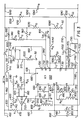
electronic ballast system 10 provides a pair ofleads lead 120 for coupling to a ground connection.Leads filter circuit 12 ofballast system 10. The filter circuit is intended to prevent high frequency signals generated withinballast system 10 from feeding back through the AC power lines, and also to prevent high frequency transients from interfering with the ballast system circuits. The input tofilter circuit 12 is provided with a standard capacitance filtering arrangement wherein acapacitor 140 is coupled betweenline 100 andline 120 by means of theconnection lines capacitor 160 is coupled between the opposingpower line lead 110 andground 120, andcapacitor 180 is coupled in parallel relation to bothcapacitors capacitor 180 being coupled on opposing ends torespective lines Capacitors capacitor 180 is a 0.1µf, 250 V. capacitor.Lines shunt filter capacitor 180 to acommon mode choke 190, providing a series inductance to each oflines Common mode choke 190 is a commercially available component, and my have a manufacturer's designation B82723-A2102-N1, available from Siemens Components, Inc. of Mt. Laurel, N.J. - The output from
common mode choke 190 is coupled to a capacitance filter arrangement similar to that provided on the input ofchoke 190. Capacitor 210, being a 1000 pf, 250 V. capacitor, is coupled between thechoke output line 280 andground connection 50, whilecapacitor 230, being identical tocapacitor 210, is coupled between the opposingchoke output line 285 andground connection 250. Capacitor 330, being a 0.33µf, 250 V. capacitor, is coupled in parallel relationship with the series combination ofcapacitors - In order to protect against high voltage surges which may be transmitted by the AC power lines, such as may be caused by lightning strikes or switching of large loads,
metal oxide varistor 240 is coupled in parallel relation withcapacitor 330 across the common modechoke output lines Varistor 240 may be any of a number of commercially available components, one such varistor may have a designation TNR9G471KM, available from Marcon America Corp. of Vernon Hills, Ill. - The common mode
choke output lines 280 are coupled to a full wave rectification bridge circuit formed by thediodes Diodes electronic ballast system 10,diode elements - The rectified voltage supplied from
diodes lines DC output line 370 there is provided a current limitingresistor 380, having a resistance or 5.0 ohms, for limiting the inrush current whenelectronic ballast system 10 is first energized.Resistor 380 is coupled in series relation with therectifier output line 370 and the regulated power supplycircuit input line 450. -
Filter capacitor 430 is coupled between regulated powersupply input line 450 and therectifier return line 1175 for providing a standard smoothing function for the pulsating DC voltage. Capacitor 430 is a 0.1µf, 450 V. capacitor. In parallel relation withcapacitor 430 there is provided atransient protection diode 400 for suppressing transient voltages.Transient protection diode 400 provides added protection from voltage surges, and while it is intended to suppress transience of lower magnitude thanmetal oxide varistor 240, its switching speed is considerably faster, thereby providing protection from steep wavefront surges. Transient protection may be a commercially available component having a designation BZWO4-376, available from General Instruments of Hicksville, N.Y. - Referring now to FIG. 3 there is shown the regulated
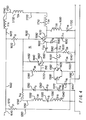
power supply circuit 14 of universalelectronic ballast system 10. As will be explained in following paragraphs, the regulated power supply circuit depends on operation of the switchingcircuit 16, FIG. 4, for its operation. But, initially the unregulated DC voltage from regulated powersupply input line 450 is supplied to the switchingcircuit 16.Diode 510 being coupled in series relation with regulated powersupply input line 450 and regulated powersupply output line 1640 provides the path for the unregulated voltage during the initial start-up ofballast system 10.Diode 510 is a commercially available 1N4006 diode. - Referring now to FIG. 4, there is shown the switching
circuit 16 ofelectronic ballast system 10. During initial start-up, the unregulated voltage supplied online 1640 is conducted toline 1660, transformer winding 1740, output transformer primary winding 1730 and transformer winding 1710 to thecollector 1610 of switchingtransistor 1590. Initially,transistor 1590 is in an "off" condition, butresistor 1620, being a 360 Kohm resistor, and having one end coupled toline 1660 and the opposing end coupled to thebase 1630 oftransistor 1590 provides a conductive path to initially turntransistor 1590 "on". Astransistor 1590 is turned "on", current begins to flow throughwindings transistor 1590, fromcollector 1610 toemitter 1600, through the series coupleddiodes 1580 and 1560, throughresistor 1540, having a value approximating 0.64 ohms, and back to thereturn line 1175. The flow of current through thewindings such transistor 1590 which has been successfully utilized has the designation MUE8502, available from Motorola, Inc. of Tempe, Az.Diodes 1580 and 1560 may have a commercial designation of 1N4001. - The base drive circuit for
transistor 1590 comprises a secondary winding 1340 of transformer T1 having a first end coupled to thereturn line 1175 and the opposing end coupled to acapacitor 1320, being a 0.22µf, 100 V. capacitor. The opposing end ofcapacitor 1320 is coupled in series relation with secondary winding 1300 of transformer T3. The opposing end of winding 1300 is coupled in series relationship withresistor 1290, having a value of 300 ohms, which is in turn coupled to thebase 1630 oftransistor 1590. By virtue of the magnetic coupling between primary winding 1710 of transformer T3 and secondary winding 1300 a voltage is induced in winding 1300 responsive to the voltage induced by the change of current through primary winding 1710. Similarly, secondary winding 1340 of transformer T1 is magnetically coupled to the primary winding 1740 for inducing a voltage across secondary winding 1340 responsive to the induced voltage of primary winding 1740, as is well known in the transformer art. Transformer T1 is formed on a toroidal core having a designation F41206, available from Magnetics, Inc. of East Butler, Pa. Winding 1740 is formed of 1 turn, and winding 1340 is formed by 10 turns. - As indicated by the dot convention, shown in FIG. 4, the voltages induced in
windings transistor 1590. Thus, as current begins to flow in the collector circuit a positive feedback voltage is generated within thewindings transistor 1590 to a full "on" condition. The voltages induced in the windings are additive, and the rate of change of the base current is a function of the LC time constant of the base drive circuit. - The LC time constant being a function of the inductance of
windings capacitor 1320.Resistor 1290 coupled in series between the winding 1300 andbase 1630 oftransistor 1590 functions as a current limiting resistor for providing a nominal base current of a predetermined value, to provide sufficient base current for the particular type oftransistor 1590 utilized in the circuit. - Transformer T3 is formed using a commercially available core having a designation P43524, available from Magnetics, Inc., with a tapped primary winding by winding
portions windings collector 1610 oftransistor 1590. The connection of the primary winding of transformer T3 in this fashion provides an autotransformer configuration for the subsequent generation of the high voltage necessary to actuate thegas discharge lamp 1900. - Subsequent to
transistor 1590 being driven to an "on" condition, the collector current flowing throughwindings capacitor 1700 coupled between one end of winding 1680 and thereturn line 1175.Capacitor 1700 is a 3.3 nf, 1600 V. capacitor. The collector current reaches its steady state value in a time period controlled by the LC time constant of the collector circuit, which becomes controlling after the initial start up. This time constant is a function of the inductance ofwindings capacitor 1700. The inductance of winding 1730 is a function of both the inductance of the winding 1730 itself, and the reflected impedance from the secondary circuit, whose most significant impedance is the capacitance ofcapacitor 1940, shown in FIG. 5. - As is well known from classical theory, transformer action only takes place when there is a change in current flow. Thus, as the steady state collector current is reached the voltage polarities of the transformer
primary windings secondary windings windings transistor 1590. The rapid turn-off oftransistor 1590 creates a rapid change of rate for the current flow which was formerly flowing throughtransistor 1590. The energy stored in the magnetic fields of each of the windings of the collector circuit discharge by the self-induction of a voltage. Winding 1680 and winding 1710 provides a high voltage, which is utilized for operation of the gas discharge lamp, as will be more fully described in following paragraphs. As was the case for the first half of the cycle, when the rate of change in current flow approaches a steady state value the voltage polarity inwindings transistor 1590 to an "on" condition, thereby providing a repetitive cycle. - Referring back to FIG. 3, the operation of the regulated
power supply circuit 14 and its interrelationship with the switchingcircuit 16 can now be described.Control circuit 660 is an integrated circuit containing the essential elements for constructing a switching power supply having sinusoidal line-current consumption.Integrated circuit 660 has a Manufacturer's Designation Number TDA4814A, available from Siemens Components, Inc., of Santa Clara, Calif. In the ordinary application ofcontrol circuit 660, theintegrated circuit 660 would be coupled to the unregulated DC voltage supply to provide actuating power therefor. However, universalelectronic ballast system 10 uniquely provides a feedback voltage generated responsive to oscillation of the switchingcircuit 16 for poweringintegrated circuit 660 and theperipheral amplifier circuits - Secondary winding 820 of transformer T3, having 12 turns, is coupled in series relation with
diode 810 to provide a rectified voltage from the AC voltage generated in winding 820 responsive to the repetitive operation of switchingcircuit 16, wherein an alternating current flows through transformer T3primary windings control circuit 660, terminal 670 being the ground coupling connection for the integrated circuit. The opposing end of winding 820 is coupled to the anode ofdiode 810, the cathode ofdiode 810 being coupled in series relation with current limitingresistor 800.Diode 810 is a 1N4148 diode andresistor 800 has a value of 270 ohms. The opposing end ofresistor 800 being coupled toterminal 680 ofcontrol circuit 660 and thepower input line 790 forintegrated circuit comparators diode 810 andresistor 800 is filtered by a 10µf storage capacitor 830 coupled in parallel relation with the series combination of aforementioned elements. In shunt relation withstorage capacitor 830 there is provided a 0.1µf bypass capacitor 840 for providing high frequency filtering of the voltage supplied tointegrated circuit 660 andcomparators Comparators return line 795.Comparators - Subsequent to being energized, integrated
circuit 660 provides a pulsating drive signal totransistor 540 by means of the coupling betweengate 930 andterminal 700.Transistor 540 is a power field effect transistor having the Manufacturer's Designation MTP2N50, available from Motorola, Inc. of Tempe. Az. Responsive to the voltage applied togate 930 oftransistor 540,transistor 540 turns "on", providing a conductive path between thedrain 550 andsource 560. Thesource 560 oftransistor 540 is coupled in series relation with aresistor 1020, having a low resistance value approximating 0.33 Ohms, whose function will be more fully understood in following paragraphs. The low impedance path betweenline 520 and the power supply common 50 provides a significant current flow from the unregulated voltagepower input line 450 throughline 530, and through the voltage boost primary transformer winding 500 of transformer T4. As previously stated, the drive signal supplied fromterminal 700 ofintegrated circuit 660 is a pulsating signal, having a frequency approximating 30 khz, for alternately switchingtransistor 540 between "on" and "off" conditions. Transformer T4 is formed on a commercially available core having a designation P42510, available from Magnetics, Inc., with winding 500 having 180 turns and winding 900 having 36 turns. - Responsive to the sudden discontinuance of current flow through
transistor 540 when the transistor is switched off, a voltage is induced within primary winding 500 of transformer T4, which is substituted for the unregulated voltage previously supplied to thediode 510. The voltage generated by winding 500 is supplied to the regulatedvoltage output line 1640 by means of thediode 990. The anode ofdiode 990 is coupled toline 520 for supplying the induced voltage thereto. The cathode ofdiode 990 is coupled tooutput line 1640, thereby providing the series combination of winding 500 anddiode 990 coupled in parallel relationship with thediode 510. Thus by designing winding 500 to generate a voltage greater than the unregulated voltage supplied online 450, suchreverse biases diode 510, thereby replacing the unregulated voltage previously coupled tooutput line 1640 bydiode 510 with the voltage induced in winding 500.Diode 990 is commercially available and has a designation of 1N4937. - In order to regulate this induced voltage, a number of feedback signals must be provided to the
control circuit 660. The first of these feedback signals is provided from the voltage divider formed by the series coupledresistors Resistor 470, having a value of 1.0 megohms, is coupled on one end to the unregulated powersupply input line 450, and on the opposing end to theinput terminal 770 and one end of the 7.5Kohm resistor 870, the opposing end ofresistor 870 being coupled to thepower supply return 50.Resistor 870 is shunted by afilter 10 nf.capacitor 850, provided for decoupling any transient variations in the feedback signal supplied to input terminal 770. Thus, the voltage supplied by the voltage divider to input terminal 770 is proportional to the unregulated DC voltage supplied to the regulated powersupply input line 450. Responsive to changes in the unregulated input voltage supplied atline 450, integratedcircuit 660 modulates the pulse width of the pulsating drive signal supplied fromterminal 700 for changing the relative "on" and "off" times oftransistor 540, whereby the induced voltage from winding 500 is adjusted to compensate for any change in input voltage. - To more finely regulate the voltage generated, a second monitoring voltage divider is provided at the output of the regulated power supply circuit.
Resistor 1210, having a value approximating 1.1 megohms, is coupled on one end to the regulated powersupply output line 1640 and on the opposing end to thecomparator input lead 1170 by way ofconnection line 1110 and one end of a 4.99Kohm resistor 1230, the opposing end ofresistor 1230 being coupled to thepower supply return 50. Thus, the voltage supplied to thecomparator input line 1170 from thecoupling node 1240 betweenresistors voltage output line 1640. The opposinginput lead 1160 ofcomparator 1120 is coupled to a reference voltage supplied byterminal 740 ofcontrol circuit 660 for use bycomparator 1120 in generating an error signal at thecomparator output line 1130, which provides feedback to controlcircuit 660.Capacitor 1140, having a value of 0.1 µf., is coupled between thereference voltage terminal 740 and thepower supply return 50 for decoupling any high frequency signals therefrom. Similarly, .001 µf. capacitor 1100 is coupled betweeninput terminals comparator 1120. - The output of
comparator 1120 is coupled to theinput terminal 770 ofintegrated circuit 660 for further affecting the pulse width modulation of the output drive signal responsive to changes in load conditions which might otherwise affect the output voltage supplied toline 1640. -
Control circuit 660 maintains a sinusoidal line-current load for the AC power supply mains, thereby substantially eliminating harmonic frequency generation typically produced by switching-type power supplies. In order to control the switching oftransistor 540 so as to prevent gaps in the current flowing through winding 500, integratedcircuit 660 must monitor the current through winding 500, the current flowing throughtransistor 540 and the phase relationship between the voltage generated and the current. - The current through winding 500 of transformer T4 is monitored by virtue of the secondary winding 900 coupled to
terminal 760 ofintegrated circuit 660 by means of the series coupled 47Kohm resistor 890. Thus, the secondary winding 900 is coupled on one end to thepower supply return 50 and on the opposing end to one end ofresistor 890, whose opposing end is coupled to theinput terminal 760. Coupled in parallel relationship with the series combination of winding 900 andresistor 890 is a voltage divider formed by the series combination of resistors 920 and 910, having values of 150 Kohms and 2.2 Kohms, respectively. The node therebetween being coupled to theinput terminal 750, for providing a "START" signal for use internal to the integrated circuit. The current flowing throughtransistor 540 is monitored by means of thesource resistor 1020, providing a voltage thereacross proportional to the current flow therethrough. This voltage is fed back to integratedcircuit 660 by means of thecoupling line 635 coupled between thesource 570 oftransistor 540 and theinput terminal 690 ofcontrol circuit 660. - Additionally, the current flowing through the
transistor 540 is further monitored by thecomparator 1125. The voltage acrosssource resistor 1020 is coupled to 3.32 Kohm resistor 630 which in turn is coupled tocomparator input line 610, for comparison with a predetermined reference voltage supplied to thecomparator input 620. This predetermined comparator reference voltage is generated by a voltage divider formed by the series combination ofresistors Kohm resistor 600 is coupled to the referencevoltage output terminal 740 and the opposing end ofresistor 600 being coupled to one end of 4.99Kohm resistor 580, the opposing end ofresistor 580 being coupled to thepower supply return 50. The coupling node betweenresistors comparator input line 620 for providing the predetermined reference voltage thereto. A .001µf.bypass capacitor 590 is coupled between thecomparator input lines comparator 1125 is coupled to theinput terminal 770, as was thecomparator 1120 for providing gain responsive regulation of the operation oftransistor 540. -
Control circuit 660 monitors the ripple on the output voltage through a voltage divider formed byresistor 1070, having a value approximating 1.1 megohms, and a 4.99Kohm resistor 1090, coupled in series relation between the DCvoltage output line 1640 and the power supply common 50. Thenode therebetween resistors line 1640. That proportional voltage is supplied to controlcircuit 660 by means of the voltage divider network and frequencytrap comprising resistors 1040, 1050, having values of 20 Kohms and 200 Kohms, respectively, and 0.1 µf.capacitor 1060. Theresistor 1050 being coupled in parallel relation with thecapacitor 1060 between theterminals integrated circuit 660. This filter trap provides an error signal representing the ripple voltage, which is undesired, on the regulated DC output supplied atline 1640. The signals input toterminals terminal 700 to thegate 930 oftransistor 540. -
Control circuit 660 also requires a logic input for initiating the operation of the internal circuitry, which is provided by a voltage input to theterminal 710 ofcontrol circuit 660. This voltage input is provided by the resistor diode network formed byresistors diode 980.Resistor 960, having a value of 1.0 megohms, is coupled on one end to regulatedoutput voltage line 1640 and on the opposing end toterminal 710 by means of thecoupling line 940 and to one end of the 470ohm resistor 970. The opposing end ofresistor 970 is coupled in series relation with the anode ofdiode 980, the cathode ofdiode 980 being coupled to the anode ofdiode 990. Theinput terminal 710 is coupled to a 0.001 µf.bypass capacitor 950 by means of thecoupling line 940, whereby high frequency transients are coupled to thepower supply return 50.Diode 980 may be a 1N4937 diode. - The regulated voltage provided on the power
supply output line 1640 is coupled to the switchinginput line 1660 for generation of a pulsating regulated current by the repetitive switching "on" and "off" oftransistor 1590, as has previously been described. The switchingcircuit 16 includes overcurrent and no-load protection circuits which operate to shut down the repetitive switching oftransistor 1590 under predetermined conditions. Further, these circuits also serve to regulate the pulsating current from which the lamp actuating voltage is generated. In addition to the current feedback provided by the tapped primary winding 1680, 1710 of induction transformer T3, the current is monitored by means of theresistor 1540, coupled in series relation with theemitter 1600 oftransistor 1590.Emitter 1600 is coupled in series relation with a pair of series coupleddiodes 1560 and 1580. provided for breakdown voltage protection, which in turn is coupled to one end ofresistor 1540, the opposing end ofresistor 1540 being coupled to thereturn line 50. A 10 µf.bypass capacitor 1550 shunts the twodiodes 1580 and 1560 for decoupling theemitter 1600 oftransistor 1590. - The voltage drop across
resistor 1540 is proportional to the emitter current flowing therethrough, thereby providing means for monitoring the switching circuit's operation. Thenode 1535 between diode 1560 andresistor 1540 is coupled to atransistor 1382 through a 200ohm resistor 1530 coupled on one end to thenode 1535 and on the opposing end to thebase 1470 oftransistor 1382. A 2200 pf.capacitor 1500 is coupled between the base and emitter oftransistor 1382 for the decoupling thereof.Transistor 1382 is an NPN type transistor having the Designation Number 2N2222A manufactured by National Semiconductor of Santa Clara, Ca. The collector oftransistor 1382 is coupled to a resistor 270 ohm 1390 and thebase 1510 oftransistor 1440, by thecoupling line 1520.Resistor 1390 being coupled tocoupling line 1520 on one end is coupled to the base drive line 1430 on the opposing end.Transistor 1440 is a PNP type transistor having the Designation Number 2N3906 manufactured by National Semiconductor of Santa Clara, Ca. Theemitter 1450 oftransistor 1440 is coupled to the base drive line 1430 and thecollector 1460 is coupled to thebase 1470 oftransistor 1382. Thus, the collector-to-emitter path oftransistor 1440 is coupled in shunt relationship with the series combination of the base-to-emitter junction oftransistor 1590,diodes 1580 and 1560, andresistor 1530. - When the emitter current of
transistor 1590 reaches a predetermined value, the voltage drop acrossresistor 1540 is sufficient to turn "on" thetransistor 1382, thereby coupling thebase 1510 oftransistor 1440 to a potential substantially below that of theemitter 1450, turningtransistor 1440 "on". Whentransistor 1440 is turned "on" such essentially pulls the base potential oftransistor 1590 below the voltage on theemitter 1600, forcingtransistor 1590 to an "off" condition. While such a circuit configuration could be utilized for strictly overcurrent protection, by selecting the maximum allowable current as a function of the operating parameters forelectronic ballast system 10, this "shut down" circuit functions to aid in regulation of the pulsating switching current. - While the LC time constants provided in the base and collector circuits operate to control the overall oscillation frequency and "on-time" of the transistor, the turn-off time is significantly affected by the transistor's storage time and its gain. By responding to the emitter current,
transistor 1590 can be turned off prematurely, with respect to the oscillation frequency established by the base drive circuit, and thereby compensate for these transistor characteristics which would tend to extend the "on" time of the transistor. In this wayelectronic ballast system 10 is able to compensate for variations between onetransistor 1590 and another. Thebase 1630 oftransistor 1590 is protected from negative voltage spikes by a reversed biased diode string, as is well known in the art.Diodes transistor 1590. The anode ofdiode 1370 is coupled to the powersupply return line 50 and the cathode ofdiode 1350 is coupled to the base drive line 1430. Each ofdiodes - As previously stated, when
transistor 1590 is conducting, current flows through the tapped primary winding formed by thewindings transistor 1590 is turned "off", induces a high voltage in winding 1680, which is added to the voltage induced in winding 1710 to cause a current to flow which is substantially equal to that which was flowing through the windings just prior to the transistor turning "off". The voltages generated by this inductive "kick" is of opposite polarity to that which was dropped across the inductive impedances when the transistor was in an "on" condition, and thereby changes the polarity of the voltage induced in the base drive circuit, which reinforces the "off" condition. Here again, when the current flow betweenline 1660 and thepower supply return 50 throughwindings capacitor 1700 approaches a steady state value, the "turn-on" sequence repeats. - The voltages induced are coupled to the
gas discharge lamp 1900 by means of the output transformer T2 through the magnetic coupling with primary winding 1730. Transformer T2 is formed on a commercially available core having a designation number P43007 available from Magnetics, Inc. of East Butler, Pa. Primary winding 1730 is formed with 90 turns, secondary winding 1765 is formed with 180 turns, secondary winding 2040 has 3 turns, and secondary winding 1790 includes 7 turns. As shown in Fig. 5, the actuation voltage supplied togas discharge lamp 1900 is induced in the tuned secondary winding 1765 of output transformer T2. Secondary winding 1765 is tuned by the 15nf capacitor 1940 coupled in parallel relation with the winding 1765 for generating a sinusoidal voltage. This sinusoidal voltage is coupled to the gas discharge lamp through a series coupled 0.1 µf.capacitor 2010. Additionally, output transformer T2 includes a pair offilament voltage windings respective filament filament 1870 through adiode 1810, having a designation 1N4934, for isolating the filament sense current from the filament winding 1790. - Detection of a no-load condition, when the
gas discharge lamp 1900 is removed from the circuit, is achieved by coupling a small DC current throughfilament 1870. A voltage divider is formed by the series combination ofresistors filament 1870.Resistor 1270 has a value of 470 Kohms and is coupled on one end to the switchingcircuit input line 1660 and on the opposing end tocoupling line 1280.Resistor 1830 has a value of 10 Kohms and is coupled on one end to thecoupling line 1280 and on the opposing end to one end offilament 1870, the opposing end offilament 1870 being coupled to the powersupply return line 50. Thus, whengas discharge lamp 1900 is electrically connected toelectronic ballast system 10, a current flows through theresistors filament 1870. Azener diode 1490, having a designation 1N5256B, is coupled to thenode 1840 ofcoupling line 1280 for sensing the voltage drop acrossresistor 1830 andfilament 1870. The voltage drop acrossresistor 1830 andfilament 1870 being predetermined to be below the zener voltage ofdiode 1490. The anode ofdiode 1490 is coupled to the base of atransistor 1380 which is coupled in parallel relationship with thetransistor 1382, the collectors of bothtransistors coupling line 1520 and both emitters being coupled to acoupling line 1480, which is in turn coupled to the powersupply return line 50. It can therefore be seen that eithertransistor transistor 1440 to an "on" condition, shutting down the conduction oftransistor 1590.Transistor 1380 is the same type astransistor 1382, and has the same manufacturer's designation. - When
gas discharge lamp 1900 is electrically removed from theelectronic ballast system 10, the current flowing throughresistors node 1840 to substantially the input voltage online 1660. This voltage biases thezener diode 1490, into conduction and thereby turns "on"transistor 1380. As previously stated, whentransistor 1380 is turned "on", such turns ontransistor 1440, which in turn shuts down theswitching transistor 1590. This no-load protection circuit prevents the high voltage generation which normally actuates the gas discharge lamp, when the lamp is removed from the circuit, thereby making the replacement of fluorescent type gas discharge tubes considerably safer than prior art systems. Additionally, this shut-down of the high voltage generation also ceases the induction of voltage in the secondary winding 820 of induction transformer T3. This in turn shuts down the boost voltage generated by the regulated power supply, supplying only the much lower rectified voltage supplied to the input of the regulated power supply. - It can therefore be seen that the concatenation of elements which comprise the universal
electronic ballast system 10 provides a highly efficient and extremely well regulated means for actuating a gas discharge lamp. The regulated power supply portion of the circuit having been designed to generate a boost voltage approximating 430 volts, and allows operation with AC input voltages in the range of 85-275 volts. Additionally, since the boost voltage is generated by a switching power supply having its own frequency control, electronic ballast system operates equally well on 50 and 60 cycle power systems. Lastly, improved switching circuit operation is achieved by the means by which thetransistor 1590 is quickly turned "off" at a predetermined current value for maintaining consistent circuit operation independent of the characteristics of a particular transistor1590. This regulation in combination with the resonant collector circuit allows for the actuation of a wide variety of gas discharge lamps having varying electrical characteristics and wattages which range from approximately between 20-50 watts. - Although this invention has been described in connection with specific forms and embodiments thereof, it will be appreciated that various modifications other than those discussed above may be made.
- For example, equivalent elements may be substituted for those specifically shown and described, certain features may be used independently of other features, and in certain cases, particular locations of elements may be reversed or interposed.
Claims (20)
- A universal electronic ballast system for coupling to a power source for actuating at least one gas discharge lamp having any one of a plurality of predetermined wattage ratings and having a pair of heater filaments, the system comprising:(a) filter means (Fig. 2) for coupling to said power source(100,110) for substantially suppressing spurious signals from passing into or from said power source:(b) regulated power supply means (Fig. 3) coupled to said filter means for (1) maintaining a substantially constant sinusoidal load current from said power source, and (2) providing a regulated DC voltage output (1640,1180);(c) switching means (Fig. 4) coupled to said regulated output of said regulated power supply means for generating a regulated pulsating current at a predetermined frequency; and(d) induction means coupled to said switching means for actuating said gas discharge lamp, said induction means including an output transformer (T2) coupled to said gas discharge lamp (1900), said induction means being coupled in feedback relationship (1820) to said switching means for terminating siad pulsating current responsive to said gas discharge lamp being electrically uncoupled from said output transformer.
- A system as recited in claim 1 where said switching means includes first transistor means (1590) having respective base (1630), collector (1610) and emitter elements (1600), said collector being coupled to a primary winding (1730) of said output transformer for inducing a voltage therein responsive to said pulsating current.
- A system as recited in claim 2 where said switching means includes regulation means coupled to said first transistor means for regulating said pulsating current responsive to changes in a load current represented by a change in an apparent impedance value of said output transformer primary winding.
- A system as recited in claim 3 where said regulation means includes base drive means (1340, 1300) coupled to said base of said first transistor means for generating a switching signal responsive to said pulsating current.
- A system as recited in any of claims 2 to 4 where said switching means includes protection means (1380,1382,1440) coupled to said first transistor means for (1) regulating the gain value of said switching means responsive to said pulsating current exceeding a predetermined value, and (2) terminating said switching signal responsive to a feedback signal (1840) from said induction means indicating electrical uncoupling of said gas discharge lamp.
- A system as recited in claim 5 where said protection means includes second transistor means (1440) having respective base, collector and emitter elements for shunting said switching signal from said base element of said first transistor means, said second transistor means having a collector-to-emitter path coupled in parallel relation to a base-to-emitter junction of said first transistor means.
- A system as recited in claim 6 where said protection means includes means (1270,1490,1830,1380) for detecting electrical uncoupling of said gas discharge lamp coupled to said second transistor means and said induction means.
- A system as recited in claim 7 where said detecting means includes third transistor means (1380) couple to said second transistor means (1440) for changing a bias condition of said base element of said second transistor means, responsive to said feedback signal (1840).
- A system as recited in claim 7 or 8 where said protection means includes current sensing means (1540,1382) for changing a bias condition of said base element of said second transistor means responsive to an emitter current of said first transistor means exceeding a predetermined value.
- A system as recited in any of claims 5 to 8 where said induction means includes voltage divider means (1830,1270) coupled to one of said pair of gas discharge lamp filaments for providing said feedback signal (1840) responsive to a predetermined current flow through said filament falling below a predetermined value.
- A system as recited in claim 4, or any of claims 5 to 10 when dependent on claim 4, where said base drive means includes a load current sensing transformer (T1) having a primary winding (1740) coupled in series relation with said primary winding (1730) of said output transformer, said load current sensing transformer having a secondary winding (1340) coupled in series relation with said base element of said first transistor means for regulating the magnitude of said switching signal responsive to said pulsating current.
- A system as recited in claim 11 where said base drive means further includes a collector current sensing transformer (T3) having a tapped primary winding (1710,1680) coupled in series relation with said primary winding of said output transformer, said tap of said tapped primary winding being coupled to said collector element of said first transistor means, said collector current sensing transformer having a first secondary winding (1300) coupled in series relation with said base element of said first transistor means for coupling a signal proportional to said collector current to said base of said first transistor means.
- A system as recited in claim 12 where said collector current sensing transformer further includes a second secondary winding (820) coupled to said regulated power supply means, whereby a voltage is generated for powering at least one of plurality of active elements (660,1120,1125) of said regulated power supply means responsive to generation of said pulsating current by said switching means.
- A system as recited in any preceding claim, where said regulated power supply means includes control circuit means (660) coupled to said filter means for driving a voltage boosting circuit responsive to an input signal (770) representing a magnitude of a voltage supplied from said power source.
- A system as recited in claim 14 where said regulated power supply means further includes first amplifier means (1120) having a input terminal (1170) coupled to said DC voltage output for generating a first feedback signal responsive to a magnitude of said DC voltage output, said first amplifier means having an output terminal (1130) coupled to said control circuit means for coupling said first feedback signal thereto.
- A system as recited in claim 14 or 15 where said regulated power supply means further includes secons amplifier means (1125) having an input (610) coupled to said voltage boosting circuit for generating a second feedback signal responsive to an operating current of said voltages boosting circuit, said second amplifier means having an output (480) coupled to said control circuit means for coupling said second feedback signal thereto.
- A system as recited in claim 16 when dependent on claim 15, where said voltage boosting circuit includes driver transistor means (540) coupled to said control circuit means for switching a current responsive to a modulated switching signal from said control circuit means, said modulated switching being pulse width modulated responsive to (1) said magnitude of said voltage supplied from said power source, (2) said first feedback signal, and (3) said second feedback signal.
- A universal electronic ballast system for coupling to a power source for actuating at least one gas discharge lamp having any one of a plurality of predetermined wattage ratings and having a pair of heater filaments, the system comprising:(a) filter means (Fig. 2) coupled to said power source (100,110) for substantially suppressing spurious signals from passing into or from said power source;(b) regulated power supply means (Fig. 3) coupled to said filter means for (1) maintaining a substantially constant sinusoidal load current from said power source, and (2) providing a regulated D.C. voltage output (1640,1180);(c) means (Fig. 4) for generating a regulated pulsating current coupled to said regulated output of said regulated power supply means, said pulsating current generating means includes (1) switching means (1590) having respective control, input, and output terminals (1630,1610,1630) wherein said output terminal is coupled to a return line of said regulated power supply means for generating said pulsating current, and (2) regulation means coupled to said switching means for regulating said pulsating current responsive to (1) a gain value of said switching means, and (2) a load current defined by said gas discharge lamp having a particular one of said plurality of predetermined wattage ratings; and(d) induction means coupled to said switching means for actuating said gas discharge lamp (1900), said induction means including an output transformer (T2) having least one secondary winding (1765) coupled to said gas discharge lamp.
- A system as recited in claim 18 where said regulation means includes drive means coupled to said control terminal (1590) of said switching means for generating a switching signal responsive to said pulsating current, said drive means including:a. a first current sensing transformer (T3) having a primary winding coupled to said input terminal of said switching means and a secondary winding (1300) couple to said control terminal for generating a first feedback signal; andb. a second current sensing transformer (T1) having a primary winding (1740) coupled in series relation with a primary winding (1730) of said output transformer (T2) for generating a second feedback signal, said second current sensing transformer having a secondary winding (1340) coupled in series relation with said secondary winding of said first current sensing transformer, whereby said switching signal is responsive to both said first and second feedback signals.
- A system as recited in claim 18 or 19 where said pulsating current generating means includes protection means (1440) coupled between said control and output terminals of said switching means for shunting said switching signal from said control terminal responsive to a feedback signal (1840) from said induction means indicating electrical uncoupling of said gas discharge lamp.
Applications Claiming Priority (2)
| Application Number | Priority Date | Filing Date | Title |
|---|---|---|---|
| US07/639,338 US5130611A (en) | 1991-01-16 | 1991-01-16 | Universal electronic ballast system |
| US639338 | 1991-01-16 |
Publications (3)
| Publication Number | Publication Date |
|---|---|
| EP0495571A2 true EP0495571A2 (en) | 1992-07-22 |
| EP0495571A3 EP0495571A3 (en) | 1992-09-02 |
| EP0495571B1 EP0495571B1 (en) | 1996-01-03 |
Family
ID=24563700
Family Applications (1)
| Application Number | Title | Priority Date | Filing Date |
|---|---|---|---|
| EP92300091A Expired - Lifetime EP0495571B1 (en) | 1991-01-16 | 1992-01-07 | Universal electronic ballast system |
Country Status (21)
| Country | Link |
|---|---|
| US (1) | US5130611A (en) |
| EP (1) | EP0495571B1 (en) |
| JP (1) | JPH05144584A (en) |
| KR (1) | KR920015962A (en) |
| AT (1) | ATE132685T1 (en) |
| AU (1) | AU638844B2 (en) |
| BR (1) | BR9104695A (en) |
| CA (1) | CA2051164A1 (en) |
| DE (1) | DE69207215T2 (en) |
| DK (1) | DK0495571T3 (en) |
| ES (1) | ES2081561T3 (en) |
| FI (1) | FI913043A (en) |
| GR (1) | GR3019129T3 (en) |
| IE (1) | IE920067A1 (en) |
| IL (1) | IL98625A (en) |
| MX (1) | MX9100128A (en) |
| MY (1) | MY108940A (en) |
| NO (1) | NO180320C (en) |
| NZ (1) | NZ239822A (en) |
| PT (1) | PT99139B (en) |
| ZA (1) | ZA914840B (en) |
Cited By (3)
| Publication number | Priority date | Publication date | Assignee | Title |
|---|---|---|---|---|
| WO2000024233A2 (en) * | 1998-10-16 | 2000-04-27 | Electro-Mag International, Inc. | Ballast circuit |
| US6169375B1 (en) | 1998-10-16 | 2001-01-02 | Electro-Mag International, Inc. | Lamp adaptable ballast circuit |
| WO2001010176A1 (en) * | 1999-07-30 | 2001-02-08 | Koninklijke Philips Electronics N.V. | Modular high frequency ballast architecture |
Families Citing this family (9)
| Publication number | Priority date | Publication date | Assignee | Title |
|---|---|---|---|---|
| US5287040A (en) * | 1992-07-06 | 1994-02-15 | Lestician Ballast, Inc. | Variable control, current sensing ballast |
| US5389857A (en) * | 1993-05-17 | 1995-02-14 | Bruce Industries, Inc. | Magnetic ballast for fluorescent lamps |
| US5869935A (en) * | 1997-05-07 | 1999-02-09 | Motorola Inc. | Electronic ballast with inverter protection circuit |
| US6255783B1 (en) | 1998-03-17 | 2001-07-03 | Ventex Group Llc | Gas discharge lamp power supply with feed forward compensation for input voltage variations |
| US6366032B1 (en) | 2000-01-28 | 2002-04-02 | Robertson Worldwide, Inc. | Fluorescent lamp ballast with integrated circuit |
| US6919694B2 (en) * | 2003-10-02 | 2005-07-19 | Monolithic Power Systems, Inc. | Fixed operating frequency inverter for cold cathode fluorescent lamp having strike frequency adjusted by voltage to current phase relationship |
| US7829973B2 (en) * | 2007-08-23 | 2010-11-09 | Lsi Corporation | N cell height decoupling circuit |
| US7486030B1 (en) * | 2007-10-18 | 2009-02-03 | Pwi, Inc. | Universal input voltage device |
| DE102009019625B4 (en) * | 2009-04-30 | 2014-05-15 | Osram Gmbh | A method of determining a type of gas discharge lamp and electronic ballast for operating at least two different types of gas discharge lamps |
Citations (5)
| Publication number | Priority date | Publication date | Assignee | Title |
|---|---|---|---|---|
| EP0059064B1 (en) * | 1981-02-21 | 1985-10-02 | THORN EMI plc | Lamp driver circuits |
| GB2208980A (en) * | 1987-08-21 | 1989-04-19 | Transtar Limited | Power supply for fluorescent lamp |
| EP0351012A2 (en) * | 1988-07-15 | 1990-01-17 | Koninklijke Philips Electronics N.V. | Fluorescent lamp controllers |
| EP0359860A1 (en) * | 1988-09-23 | 1990-03-28 | Siemens Aktiengesellschaft | Device and method for operating at least one discharge lamp |
| EP0399613A2 (en) * | 1989-05-26 | 1990-11-28 | Philips Electronics North America Corporation | Fluorescent lamp controllers with dimming control |
Family Cites Families (23)
| Publication number | Priority date | Publication date | Assignee | Title |
|---|---|---|---|---|
| US4075476A (en) * | 1976-12-20 | 1978-02-21 | Gte Sylvania Incorporated | Sinusoidal wave oscillator ballast circuit |
| US4127795A (en) * | 1977-08-19 | 1978-11-28 | Gte Sylvania Incorporated | Lamp ballast circuit |
| US4277726A (en) * | 1978-08-28 | 1981-07-07 | Litton Systems, Inc. | Solid-state ballast for rapid-start type fluorescent lamps |
| US4259616A (en) * | 1979-07-09 | 1981-03-31 | Gte Products Corporation | Multiple gaseous lamp electronic ballast circuit |
| US4344122A (en) * | 1980-09-05 | 1982-08-10 | General Electric Company | Current sourced inverter with saturating output transformer |
| US4353009A (en) * | 1980-12-19 | 1982-10-05 | Gte Products Corporation | Dimming circuit for an electronic ballast |
| US4562383A (en) * | 1981-07-31 | 1985-12-31 | Siemens Aktiengesellschaft | Converter |
| US4414491A (en) * | 1981-08-10 | 1983-11-08 | Quietlite International, Ltd. | Current limiting power supply for electron discharge lamps |
| US4503361A (en) * | 1982-02-02 | 1985-03-05 | Intent Patent A.G. | Electronic ballast system |
| US4414492A (en) * | 1982-02-02 | 1983-11-08 | Intent Patent A.G. | Electronic ballast system |
| US4481460A (en) * | 1982-02-08 | 1984-11-06 | Siemens Aktiengesellschaft | Inverter with charging regulator having a variable keying ratio |
| DE3246454A1 (en) * | 1982-12-15 | 1984-06-20 | Siemens AG, 1000 Berlin und 8000 München | INVERTER WITH A LOAD CIRCUIT CONTAINING A SERIES RESONANCE CIRCUIT AND A DISCHARGE LAMP |
| DE3247863A1 (en) * | 1982-12-23 | 1984-06-28 | Siemens AG, 1000 Berlin und 8000 München | ARRANGEMENT FOR SWITCHING OFF A INVERTER |
| US4503362A (en) * | 1983-06-01 | 1985-03-05 | Intent Patent A.G. | Frequency stabilized, gain controlled ballast system |
| US4587461A (en) * | 1983-06-01 | 1986-05-06 | Intent Patents A.G. | Self-regulating electronic ballast system |
| US4609850A (en) * | 1983-06-01 | 1986-09-02 | Intent Patents A.G. | Current driven gain controlled electronic ballast system |
| US4613934A (en) * | 1984-03-19 | 1986-09-23 | Pacholok David R | Power supply for gas discharge devices |
| US4716343A (en) * | 1985-11-15 | 1987-12-29 | Universal Manufacturing Corporation | Constant illumination, remotely dimmable electronic ballast |
| DE3608615A1 (en) * | 1986-03-14 | 1987-09-17 | Patent Treuhand Ges Fuer Elektrische Gluehlampen Mbh | CIRCUIT ARRANGEMENT FOR OPERATING LOW-PRESSURE DISCHARGE LAMPS |
| DE3623749A1 (en) * | 1986-07-14 | 1988-01-21 | Patent Treuhand Ges Fuer Elektrische Gluehlampen Mbh | CIRCUIT ARRANGEMENT FOR OPERATING LOW-PRESSURE DISCHARGE LAMPS |
| US4902938A (en) * | 1986-11-15 | 1990-02-20 | Magnetek Inc. | Electronic ballast with high voltage protection |
| US4970439A (en) * | 1989-04-28 | 1990-11-13 | Minnesota Mining And Manufacturing Company | Power supply circuit for a gaseous discharge tube device |
| US5055747A (en) * | 1990-07-20 | 1991-10-08 | Intent Patents A.G. | Self-regulating, no load protected electronic ballast system |
-
1991
- 1991-01-16 US US07/639,338 patent/US5130611A/en not_active Expired - Fee Related
- 1991-06-20 FI FI913043A patent/FI913043A/en not_active Application Discontinuation
- 1991-06-24 ZA ZA914840A patent/ZA914840B/en unknown
- 1991-06-26 IL IL9862591A patent/IL98625A/en not_active IP Right Cessation
- 1991-06-27 AU AU79393/91A patent/AU638844B2/en not_active Ceased
- 1991-06-27 NO NO912540A patent/NO180320C/en unknown
- 1991-07-08 MX MX9100128A patent/MX9100128A/en not_active IP Right Cessation
- 1991-07-09 MY MYPI91001237A patent/MY108940A/en unknown
- 1991-07-19 JP JP3203637A patent/JPH05144584A/en not_active Withdrawn
- 1991-07-25 KR KR1019910012802A patent/KR920015962A/en not_active Application Discontinuation
- 1991-09-11 CA CA002051164A patent/CA2051164A1/en not_active Abandoned
- 1991-09-16 NZ NZ23982291A patent/NZ239822A/en unknown
- 1991-10-02 PT PT99139A patent/PT99139B/en not_active IP Right Cessation
- 1991-10-30 BR BR919104695A patent/BR9104695A/en not_active Application Discontinuation
-
1992
- 1992-01-07 DK DK92300091.3T patent/DK0495571T3/en active
- 1992-01-07 DE DE69207215T patent/DE69207215T2/en not_active Expired - Fee Related
- 1992-01-07 AT AT92300091T patent/ATE132685T1/en active
- 1992-01-07 ES ES92300091T patent/ES2081561T3/en not_active Expired - Lifetime
- 1992-01-07 EP EP92300091A patent/EP0495571B1/en not_active Expired - Lifetime
- 1992-01-08 IE IE006792A patent/IE920067A1/en not_active Application Discontinuation
-
1996
- 1996-02-28 GR GR960400553T patent/GR3019129T3/en unknown
Patent Citations (5)
| Publication number | Priority date | Publication date | Assignee | Title |
|---|---|---|---|---|
| EP0059064B1 (en) * | 1981-02-21 | 1985-10-02 | THORN EMI plc | Lamp driver circuits |
| GB2208980A (en) * | 1987-08-21 | 1989-04-19 | Transtar Limited | Power supply for fluorescent lamp |
| EP0351012A2 (en) * | 1988-07-15 | 1990-01-17 | Koninklijke Philips Electronics N.V. | Fluorescent lamp controllers |
| EP0359860A1 (en) * | 1988-09-23 | 1990-03-28 | Siemens Aktiengesellschaft | Device and method for operating at least one discharge lamp |
| EP0399613A2 (en) * | 1989-05-26 | 1990-11-28 | Philips Electronics North America Corporation | Fluorescent lamp controllers with dimming control |
Cited By (4)
| Publication number | Priority date | Publication date | Assignee | Title |
|---|---|---|---|---|
| WO2000024233A2 (en) * | 1998-10-16 | 2000-04-27 | Electro-Mag International, Inc. | Ballast circuit |
| WO2000024233A3 (en) * | 1998-10-16 | 2000-09-21 | Electro Mag Int Inc | Ballast circuit |
| US6169375B1 (en) | 1998-10-16 | 2001-01-02 | Electro-Mag International, Inc. | Lamp adaptable ballast circuit |
| WO2001010176A1 (en) * | 1999-07-30 | 2001-02-08 | Koninklijke Philips Electronics N.V. | Modular high frequency ballast architecture |
Also Published As
| Publication number | Publication date |
|---|---|
| PT99139B (en) | 1999-01-29 |
| JPH05144584A (en) | 1993-06-11 |
| EP0495571B1 (en) | 1996-01-03 |
| DE69207215T2 (en) | 1996-05-15 |
| IE920067A1 (en) | 1992-07-29 |
| DK0495571T3 (en) | 1996-02-05 |
| IL98625A0 (en) | 1992-07-15 |
| KR920015962A (en) | 1992-08-27 |
| NO912540D0 (en) | 1991-06-27 |
| CA2051164A1 (en) | 1992-07-17 |
| AU638844B2 (en) | 1993-07-08 |
| NO180320C (en) | 1997-04-02 |
| MY108940A (en) | 1996-11-30 |
| ATE132685T1 (en) | 1996-01-15 |
| US5130611A (en) | 1992-07-14 |
| FI913043A (en) | 1992-07-17 |
| MX9100128A (en) | 1992-07-01 |
| EP0495571A3 (en) | 1992-09-02 |
| NZ239822A (en) | 1994-07-26 |
| ES2081561T3 (en) | 1996-03-16 |
| IL98625A (en) | 1996-10-31 |
| NO912540L (en) | 1992-07-17 |
| FI913043A0 (en) | 1991-06-20 |
| BR9104695A (en) | 1992-09-29 |
| NO180320B (en) | 1996-12-16 |
| PT99139A (en) | 1993-10-29 |
| GR3019129T3 (en) | 1996-05-31 |
| ZA914840B (en) | 1992-04-29 |
| AU7939391A (en) | 1992-07-23 |
| DE69207215D1 (en) | 1996-02-15 |
Similar Documents
| Publication | Publication Date | Title |
|---|---|---|
| US5177408A (en) | Startup circuit for electronic ballasts for instant-start lamps | |
| US6304039B1 (en) | Power supply for illuminating an electro-luminescent panel | |
| US5592054A (en) | Fluorescent lamp ballast with selectable power levels | |
| US4132925A (en) | Direct current ballasting and starting circuitry for gaseous discharge lamps | |
| US4189663A (en) | Direct current ballasting and starting circuitry for gaseous discharge lamps | |
| US5638262A (en) | Method and apparatus for providing isolated power sourced from bleeder current | |
| EP0098285B1 (en) | Electronic high frequency controlled device for operating gas discharge lamps | |
| US4503362A (en) | Frequency stabilized, gain controlled ballast system | |
| WO1982001637A1 (en) | Electronic ballast circuit | |
| US6204613B1 (en) | Protected dimming control interface for an electronic ballast | |
| US5130611A (en) | Universal electronic ballast system | |
| US6233165B1 (en) | Power converter having a low voltage regulator powered from a high voltage source | |
| JPH0527339B2 (en) | ||
| EP0259889A2 (en) | Switching regulator type power supply circuit | |
| EP0061730A2 (en) | Transistor inverter device | |
| JP2954809B2 (en) | Switching regulator | |
| JPH06325886A (en) | High frequency lighting device | |
| US6492780B1 (en) | Lamp ballast system | |
| KR100520090B1 (en) | Switching Mode Power Supplies with Overvoltage Protection Circuits | |
| JPH09285121A (en) | Power circuit | |
| KR20000015607A (en) | Over power protection circuit of a monitor | |
| KR200156513Y1 (en) | Apparatus for protecting a smps in a monitor | |
| KR200172696Y1 (en) | Over voltage protection circuit | |
| KR870002137B1 (en) | Operating circuit of a discharge lamp | |
| KR910007048Y1 (en) | Base driving circuit of main switching tr |
Legal Events
| Date | Code | Title | Description |
|---|---|---|---|
| PUAI | Public reference made under article 153(3) epc to a published international application that has entered the european phase |
Free format text: ORIGINAL CODE: 0009012 |
|
| PUAL | Search report despatched |
Free format text: ORIGINAL CODE: 0009013 |
|
| AK | Designated contracting states |
Kind code of ref document: A2 Designated state(s): AT BE CH DE DK ES FR GB GR IT LI LU NL SE |
|
| AK | Designated contracting states |
Kind code of ref document: A3 Designated state(s): AT BE CH DE DK ES FR GB GR IT LI LU NL SE |
|
| 17P | Request for examination filed |
Effective date: 19930217 |
|
| 17Q | First examination report despatched |
Effective date: 19940926 |
|
| GRAA | (expected) grant |
Free format text: ORIGINAL CODE: 0009210 |
|
| AK | Designated contracting states |
Kind code of ref document: B1 Designated state(s): AT BE CH DE DK ES FR GB GR IT LI LU NL SE |
|
| REF | Corresponds to: |
Ref document number: 132685 Country of ref document: AT Date of ref document: 19960115 Kind code of ref document: T |
|
| REG | Reference to a national code |
Ref country code: DK Ref legal event code: T3 |
|
| REF | Corresponds to: |
Ref document number: 69207215 Country of ref document: DE Date of ref document: 19960215 |
|
| ET | Fr: translation filed | ||
| REG | Reference to a national code |
Ref country code: CH Ref legal event code: NV Representative=s name: MICHELI & CIE INGENIEURS-CONSEILS |
|
| REG | Reference to a national code |
Ref country code: ES Ref legal event code: FG2A Ref document number: 2081561 Country of ref document: ES Kind code of ref document: T3 |
|
| ITF | It: translation for a ep patent filed |
Owner name: MARIETTI E GISLON S.R.L. |
|
| REG | Reference to a national code |
Ref country code: GR Ref legal event code: FG4A Free format text: 3019129 |
|
| PLBE | No opposition filed within time limit |
Free format text: ORIGINAL CODE: 0009261 |
|
| STAA | Information on the status of an ep patent application or granted ep patent |
Free format text: STATUS: NO OPPOSITION FILED WITHIN TIME LIMIT |
|
| 26N | No opposition filed | ||
| PGFP | Annual fee paid to national office [announced via postgrant information from national office to epo] |
Ref country code: GR Payment date: 19961230 Year of fee payment: 6 Ref country code: FR Payment date: 19961230 Year of fee payment: 6 |
|
| PGFP | Annual fee paid to national office [announced via postgrant information from national office to epo] |
Ref country code: BE Payment date: 19970103 Year of fee payment: 6 |
|
| PGFP | Annual fee paid to national office [announced via postgrant information from national office to epo] |
Ref country code: GB Payment date: 19970106 Year of fee payment: 6 |
|
| PGFP | Annual fee paid to national office [announced via postgrant information from national office to epo] |
Ref country code: ES Payment date: 19970107 Year of fee payment: 6 |
|
| PGFP | Annual fee paid to national office [announced via postgrant information from national office to epo] |
Ref country code: AT Payment date: 19970114 Year of fee payment: 6 |
|
| PGFP | Annual fee paid to national office [announced via postgrant information from national office to epo] |
Ref country code: CH Payment date: 19970116 Year of fee payment: 6 |
|
| PGFP | Annual fee paid to national office [announced via postgrant information from national office to epo] |
Ref country code: SE Payment date: 19970117 Year of fee payment: 6 |
|
| PGFP | Annual fee paid to national office [announced via postgrant information from national office to epo] |
Ref country code: DK Payment date: 19970130 Year of fee payment: 6 |
|
| PGFP | Annual fee paid to national office [announced via postgrant information from national office to epo] |
Ref country code: NL Payment date: 19970131 Year of fee payment: 6 |
|
| PGFP | Annual fee paid to national office [announced via postgrant information from national office to epo] |
Ref country code: LU Payment date: 19970212 Year of fee payment: 6 |
|
| PGFP | Annual fee paid to national office [announced via postgrant information from national office to epo] |
Ref country code: DE Payment date: 19970224 Year of fee payment: 6 |
|
| PG25 | Lapsed in a contracting state [announced via postgrant information from national office to epo] |
Ref country code: LU Free format text: LAPSE BECAUSE OF NON-PAYMENT OF DUE FEES Effective date: 19980107 Ref country code: GB Free format text: LAPSE BECAUSE OF NON-PAYMENT OF DUE FEES Effective date: 19980107 Ref country code: AT Free format text: LAPSE BECAUSE OF NON-PAYMENT OF DUE FEES Effective date: 19980107 |
|
| PG25 | Lapsed in a contracting state [announced via postgrant information from national office to epo] |
Ref country code: SE Free format text: LAPSE BECAUSE OF NON-PAYMENT OF DUE FEES Effective date: 19980108 Ref country code: ES Free format text: LAPSE BECAUSE OF EXPIRATION OF PROTECTION Effective date: 19980108 |
|
| PG25 | Lapsed in a contracting state [announced via postgrant information from national office to epo] |
Ref country code: LI Free format text: LAPSE BECAUSE OF NON-PAYMENT OF DUE FEES Effective date: 19980131 Ref country code: GR Free format text: LAPSE BECAUSE OF NON-PAYMENT OF DUE FEES Effective date: 19980131 Ref country code: FR Free format text: THE PATENT HAS BEEN ANNULLED BY A DECISION OF A NATIONAL AUTHORITY Effective date: 19980131 Ref country code: CH Free format text: LAPSE BECAUSE OF NON-PAYMENT OF DUE FEES Effective date: 19980131 Ref country code: BE Free format text: LAPSE BECAUSE OF NON-PAYMENT OF DUE FEES Effective date: 19980131 |
|
| PG25 | Lapsed in a contracting state [announced via postgrant information from national office to epo] |
Ref country code: DK Free format text: LAPSE BECAUSE OF NON-PAYMENT OF DUE FEES Effective date: 19980202 |
|
| BERE | Be: lapsed |
Owner name: INTENT PATENTS A.G. Effective date: 19980131 |
|
| PG25 | Lapsed in a contracting state [announced via postgrant information from national office to epo] |
Ref country code: NL Free format text: LAPSE BECAUSE OF NON-PAYMENT OF DUE FEES Effective date: 19980801 |
|
| GBPC | Gb: european patent ceased through non-payment of renewal fee |
Effective date: 19980107 |
|
| REG | Reference to a national code |
Ref country code: CH Ref legal event code: PL |
|
| NLV4 | Nl: lapsed or anulled due to non-payment of the annual fee |
Effective date: 19980801 |
|
| PG25 | Lapsed in a contracting state [announced via postgrant information from national office to epo] |
Ref country code: DE Free format text: LAPSE BECAUSE OF NON-PAYMENT OF DUE FEES Effective date: 19981001 |
|
| EUG | Se: european patent has lapsed |
Ref document number: 92300091.3 |
|
| REG | Reference to a national code |
Ref country code: FR Ref legal event code: ST |
|
| REG | Reference to a national code |
Ref country code: ES Ref legal event code: FD2A Effective date: 20000201 |
|
| REG | Reference to a national code |
Ref country code: DK Ref legal event code: EBP |
|
| PG25 | Lapsed in a contracting state [announced via postgrant information from national office to epo] |
Ref country code: IT Free format text: LAPSE BECAUSE OF NON-PAYMENT OF DUE FEES;WARNING: LAPSES OF ITALIAN PATENTS WITH EFFECTIVE DATE BEFORE 2007 MAY HAVE OCCURRED AT ANY TIME BEFORE 2007. THE CORRECT EFFECTIVE DATE MAY BE DIFFERENT FROM THE ONE RECORDED. Effective date: 20050107 |