EP0495679A2 - A reflective liquid crystal display device and a method for fabricating same - Google Patents
A reflective liquid crystal display device and a method for fabricating same Download PDFInfo
- Publication number
- EP0495679A2 EP0495679A2 EP19920300438 EP92300438A EP0495679A2 EP 0495679 A2 EP0495679 A2 EP 0495679A2 EP 19920300438 EP19920300438 EP 19920300438 EP 92300438 A EP92300438 A EP 92300438A EP 0495679 A2 EP0495679 A2 EP 0495679A2
- Authority
- EP
- European Patent Office
- Prior art keywords
- liquid crystal
- convex portions
- reflector
- crystal display
- reflective
- Prior art date
- Legal status (The legal status is an assumption and is not a legal conclusion. Google has not performed a legal analysis and makes no representation as to the accuracy of the status listed.)
- Granted
Links
Images


Classifications
-
- G—PHYSICS
- G02—OPTICS
- G02B—OPTICAL ELEMENTS, SYSTEMS OR APPARATUS
- G02B5/00—Optical elements other than lenses
- G02B5/02—Diffusing elements; Afocal elements
- G02B5/0205—Diffusing elements; Afocal elements characterised by the diffusing properties
- G02B5/021—Diffusing elements; Afocal elements characterised by the diffusing properties the diffusion taking place at the element's surface, e.g. by means of surface roughening or microprismatic structures
- G02B5/0215—Diffusing elements; Afocal elements characterised by the diffusing properties the diffusion taking place at the element's surface, e.g. by means of surface roughening or microprismatic structures the surface having a regular structure
-
- G—PHYSICS
- G02—OPTICS
- G02B—OPTICAL ELEMENTS, SYSTEMS OR APPARATUS
- G02B5/00—Optical elements other than lenses
- G02B5/02—Diffusing elements; Afocal elements
- G02B5/0273—Diffusing elements; Afocal elements characterized by the use
- G02B5/0284—Diffusing elements; Afocal elements characterized by the use used in reflection
-
- G—PHYSICS
- G02—OPTICS
- G02B—OPTICAL ELEMENTS, SYSTEMS OR APPARATUS
- G02B5/00—Optical elements other than lenses
- G02B5/12—Reflex reflectors
- G02B5/122—Reflex reflectors cube corner, trihedral or triple reflector type
- G02B5/124—Reflex reflectors cube corner, trihedral or triple reflector type plural reflecting elements forming part of a unitary plate or sheet
-
- G—PHYSICS
- G02—OPTICS
- G02F—OPTICAL DEVICES OR ARRANGEMENTS FOR THE CONTROL OF LIGHT BY MODIFICATION OF THE OPTICAL PROPERTIES OF THE MEDIA OF THE ELEMENTS INVOLVED THEREIN; NON-LINEAR OPTICS; FREQUENCY-CHANGING OF LIGHT; OPTICAL LOGIC ELEMENTS; OPTICAL ANALOGUE/DIGITAL CONVERTERS
- G02F1/00—Devices or arrangements for the control of the intensity, colour, phase, polarisation or direction of light arriving from an independent light source, e.g. switching, gating or modulating; Non-linear optics
- G02F1/01—Devices or arrangements for the control of the intensity, colour, phase, polarisation or direction of light arriving from an independent light source, e.g. switching, gating or modulating; Non-linear optics for the control of the intensity, phase, polarisation or colour
- G02F1/13—Devices or arrangements for the control of the intensity, colour, phase, polarisation or direction of light arriving from an independent light source, e.g. switching, gating or modulating; Non-linear optics for the control of the intensity, phase, polarisation or colour based on liquid crystals, e.g. single liquid crystal display cells
- G02F1/133—Constructional arrangements; Operation of liquid crystal cells; Circuit arrangements
- G02F1/1333—Constructional arrangements; Manufacturing methods
- G02F1/1335—Structural association of cells with optical devices, e.g. polarisers or reflectors
- G02F1/133553—Reflecting elements
-
- G—PHYSICS
- G02—OPTICS
- G02F—OPTICAL DEVICES OR ARRANGEMENTS FOR THE CONTROL OF LIGHT BY MODIFICATION OF THE OPTICAL PROPERTIES OF THE MEDIA OF THE ELEMENTS INVOLVED THEREIN; NON-LINEAR OPTICS; FREQUENCY-CHANGING OF LIGHT; OPTICAL LOGIC ELEMENTS; OPTICAL ANALOGUE/DIGITAL CONVERTERS
- G02F2201/00—Constructional arrangements not provided for in groups G02F1/00 - G02F7/00
- G02F2201/12—Constructional arrangements not provided for in groups G02F1/00 - G02F7/00 electrode
- G02F2201/121—Constructional arrangements not provided for in groups G02F1/00 - G02F7/00 electrode common or background
-
- G—PHYSICS
- G02—OPTICS
- G02F—OPTICAL DEVICES OR ARRANGEMENTS FOR THE CONTROL OF LIGHT BY MODIFICATION OF THE OPTICAL PROPERTIES OF THE MEDIA OF THE ELEMENTS INVOLVED THEREIN; NON-LINEAR OPTICS; FREQUENCY-CHANGING OF LIGHT; OPTICAL LOGIC ELEMENTS; OPTICAL ANALOGUE/DIGITAL CONVERTERS
- G02F2201/00—Constructional arrangements not provided for in groups G02F1/00 - G02F7/00
- G02F2201/12—Constructional arrangements not provided for in groups G02F1/00 - G02F7/00 electrode
- G02F2201/123—Constructional arrangements not provided for in groups G02F1/00 - G02F7/00 electrode pixel
-
- G—PHYSICS
- G02—OPTICS
- G02F—OPTICAL DEVICES OR ARRANGEMENTS FOR THE CONTROL OF LIGHT BY MODIFICATION OF THE OPTICAL PROPERTIES OF THE MEDIA OF THE ELEMENTS INVOLVED THEREIN; NON-LINEAR OPTICS; FREQUENCY-CHANGING OF LIGHT; OPTICAL LOGIC ELEMENTS; OPTICAL ANALOGUE/DIGITAL CONVERTERS
- G02F2203/00—Function characteristic
- G02F2203/02—Function characteristic reflective
-
- Y—GENERAL TAGGING OF NEW TECHNOLOGICAL DEVELOPMENTS; GENERAL TAGGING OF CROSS-SECTIONAL TECHNOLOGIES SPANNING OVER SEVERAL SECTIONS OF THE IPC; TECHNICAL SUBJECTS COVERED BY FORMER USPC CROSS-REFERENCE ART COLLECTIONS [XRACs] AND DIGESTS
- Y10—TECHNICAL SUBJECTS COVERED BY FORMER USPC
- Y10S—TECHNICAL SUBJECTS COVERED BY FORMER USPC CROSS-REFERENCE ART COLLECTIONS [XRACs] AND DIGESTS
- Y10S359/00—Optical: systems and elements
- Y10S359/90—Methods
Definitions
- the present invention relates to a reflective liquid crystal display device which does not need a backlight, and a method for manufacturing the same.
- liquid crystal display devices In rec e nt years, applications of liquid crystal display devices to word processors, lap-top personal computers, pocket-size TV displays, and the like have been in rapid progress. Especially, a reflective liquid crystal display device in which incident light is reflected to effect a display eliminates the necessity of any backlight, thereby lowering power consumption as well as reducing the size and the weight of the device.
- the conventional liquid crystal display devices mostly employ a twisted nematic (TN) mode or a super-twisted nematic (STN) mode.
- TN twisted nematic
- STN super-twisted nematic
- other display modes have been proposed in an attempt to utilize all of the natural light.
- a phase-change guest-host mode D.L. White and G.N. Taylor, J. Appl. Phys. 45, p. 4718, 1974
- a reflective multicolor display using this display mode in combination with microcolor filters has also been proposed (T. Koizumi and T. Uchida, Proceedings of the SID, vol. 29, p. 157, 1988).
- a brighter display can be obtained if the intensity of the light scattered in the direction vertical to the display screen is increased for all incident light from every direction.
- the shape of the filmed surface of a reflector for the display device should be controlled so that optimal reflective properties can be obtaIned.
- the aforementioned paper by T. Koizumi, et al. discloses a reflector which is fabricated by roughening the surface of a glass substrate with an abrasive, etching the surface with hydrofluoric acid for different periods of time thus controlling the roughness thereof and depositing a silver film on the roughened surface, so as to provide a bright reflective liquid crystal display.
- the roughened surface of the above reflector which is formed by scratching the glass substrate with the abrasive is neither uniform in shape nor reproducible. Therefore, in the above disclosed method, it is not possible to obtain a controlled uniform reproducible surface roughness on the reflector, and thus to achieve a reflective liquid crystal display device with optimal reflective properties.
- the objective of the present invention is to provide a reflective liquid crystal display device which comprises a reflector having an effective, reproducible reflective properties, and a method for fabricating such a display device.
- the reflective liquid crystal display device of this invention which overcomes the above-discussed and numerous other disadvantages and deficiencies of the prior art, comprises an insulating substrate having a transparent electrode formed thereon, a reflector including a core substrate, a number of small convex portions formed on the core substrate by patterning a photosensitive resin applied to one surface of the core substrate by use of a photomask having a predetermined pattern, and a reflective film covering the surface of the core substrate having the convex portions, and a liquid crystal layer sandwiched between the insulating substrate and the reflector.
- the surface of the reflector on which the reflective film is formed faces the liquid crystal layer.
- the reflective film of the reflector functions as a counter electrode for the transparent electrode on the insulating substrate.
- the convex portions are formed at a pitch of 100 ⁇ m or less and have a height of 10 ⁇ m or less.
- a method for fabricating a reflective liquid crystal display device having a reflector which includes a core substrate, a number of small convex portions formed on the core substrate and a reflective film covering the surface of the core substrate having the convex portions comprises the steps of patterning a photosensitive resin applied to one surface of a core substrate for the reflector by use of a photomask so as to form a number of small convex portions on the core substrate, heat-treating the core substrate having the convex portions, and forming a reflective film on the surface of the core substrate having the convex portions.
- a photosensitive resin applied to one surface of the core substrate of the reflector is patterned so as to form a predetermined shape of the convex portions thereon.
- the shape, size, and pitch of the convex portions, and the like can be optimally determined, thereby enabling the control of the reflective properties of the reflector effectively and reproducibly so as to provide a bright screen image of the display device.
- the surface of the reflector coated with the reflective film faces the liquid crystal layer, reducing the distance between the reflecting film and the liquid crystal layer and thereby effecting a reduced parallax.
- the reflective film can be used as a counter electrode for the transparent electrode on the insulating substrate.
- Figure 1 shows a reflector 17 to be used for a reflective liquid crystal display device of the present invention
- Figures 2a to 2d show the steps for fabricating the reflector 17. The procedure for fabricating the reflector 17 will be described as follows.
- a resist film 12 made of a photosensitive resin is formed on one surface of a glass core substrate 11 preferably by spinning at a speed of 500 to 3000 r.p.m.
- a glass plate No. 7059 manufactured by Corning
- the glass plate was coated with a photosensitive resin (OFPR-800 manufactured by Tokyo Ohka Kogyo Co., Ltd.) at a spinning speed of 1000 r.p.m. for 30 seconds so as to obtain the resist film 12 having a thickness of 4 ⁇ m.
- the core substrate 11 coated with the resist film 12 was prebaked at 90°C for 30 minutes.
- a photomask 13 having a predetermined pattern was disposed over the resist film 12 and light was radiated through the photomask 13 to the resist film 12, which was then treated with a developer (for example, a 2.38% solution of NMD-3 manufactured by Tokyo Ohka Kogyo Co., Ltd.) so as to form a number of fine convex portions 14 on the surface of the core substrate 11, as shown in Figure 2c.
- a developer for example, a 2.38% solution of NMD-3 manufactured by Tokyo Ohka Kogyo Co., Ltd.
- the section of the thus formed convex portions 14 is a square having substantially right angles. However, in order to cover the convex portions 14 with a reflective film 16 of a uniform thickness in a later stage, it is preferable to round the square convex portions 14.
- the inventors have found that the convex portions 14 can be easily rounded by heat treatment preferably at a temperature in the range of 120 to 250°C, more preferably at 200°C. In this example, the heat treatment was performed at 200°C for 30 minutes so as to obtain the round convex portions 14 as shown in Figure 2d.
- the surface of the core substrate 11 with the convex portions formed thereon was covered with a reflective film 16 having a uniform thickness as shown in Figure 1.
- the material for the reflective film 16 can be Al, Ni, Cr, Ag, or other metal, and the thickness thereof is preferably 0.01 to 1.0 ⁇ m.
- the reflective film 16 was formed by the vacuum evaporation of Ag. In this way, the reflector 17 was formed.
- the shape of the convex portions 14 of the reflector 17 obtained after the heat treatment is round as viewed from the top, as shown in Figure 4a.
- Other shapes such as an ellipse, a square, a rectangle, and a stripe as shown in Figures 4b to 4f are also possible.
- a diameter D1 of the round convex portions 14 shown in Figure 4a is for example 33 ⁇ m, and a lateral gap T1 and a longitudinal gap T2 between the adjacent convex portions 14 are 20 ⁇ m, respectively.
- Lateral and longitudinal distances between the centers of the adjacent convex portions 14 or pitches P1 and P2 are 53 ⁇ m and 38 ⁇ m, respectively.
- the stripe convex portions 14 of one example having a width B1 of 28 ⁇ m are formed with a gap T3 of 10 ⁇ m and a pitch P3 of 38 ⁇ m.
- the stripe convex portions 14 of another example having a width B2 of 33 ⁇ m are formed with a gap T4 of 5 ⁇ m and a pitch P4 of 38 ⁇ m.
- the elliptic convex portions 14 having a length B3 of 48 ⁇ m and a width B4 of 33 ⁇ m are formed with gaps T5 and T6 of 5 ⁇ m, a lateral pitch P5 of 53 ⁇ m and a longitudinal pitch P6 of 38 ⁇ m.
- the rectangular convex portions 14 of one example having a length B5 of 43 ⁇ m and a width B6 of 28 ⁇ m are formed with a lateral gap T7 of 10 ⁇ m, a longitudinal gap T8 of 20 ⁇ m, a lateral pitch P7 of 53 ⁇ m and a longitudinal pitch P8 of 48 ⁇ m.
- the rectangular convex portions 14 of another example having a length B7 of 48 ⁇ m and a width B8 of 33 ⁇ m are formed with gaps T9 and T10 of 5 ⁇ m, a lateral pitch P9 of 53 ⁇ m and a longitudinal pitch P10 of 38 ⁇ m.
- Figure 3 shows a method for measuring the reflective properties of the reflector fabricated as described above.
- a model 1 for measuring the reflectance is formed to imitate the state of the reflector 17 being in contact with a liquid crystal layer when the reflector 17 is disposed in an actual liquid crystal display device.
- a dummy glass substrate 2 having a refractive index of 1.5 which is substantially equal to that of an actual liquid crystal layer, and the reflector 17 and the dummy substrate 2 are sealed to each other with an ultraviolet-hardened adhesive 3.
- a photomultimeter 4 is disposed above the model 1 in the direction of the normal of the reflector 17 passing a point on the reflective film 16 irradiated with the incident ray 5. Under these conditions, a scattering ray 6 reflected by the reflector 17 is detected with the photomultimeter 4.
- the incident angle ⁇ and the angle ⁇ of the incident ray 5 are varied to measure the corresponding scattering ray 6, thereby determining the reflective properties of the reflector 17. It has been confirmed that the model 1 has the same reflective properties as the actual liquid crystal display device.
- the reflective properties of the reflectors 17 corresponding to the shapes of the convex portions 14 thereof shown in Figures 4a to 4f are shown in Figures 5a and 5b to 10a and 10b, respectively.
- the reflective intensity of the light introduced at the incident angle ⁇ is expressed as the distance from the origin O in the direction of the incident angle ⁇ .
- the chain-line curve P shows the reflective property measured for a standard white plate (magnesium oxide).
- the reflective intensity R of the light introduced at an incident angle ⁇ of 30° is shown as a function of the angle ⁇ with respect to the coordinate axes on the surface of the reflector.
- the reflective intensity R of the reflector 17 is high when the sides of the convex portion 14 of the reflector 17 are linear, and it is especially high when the light is introduced into the convex portion 14 at the right angle to the linear sizes thereof.
- the sides of the convex portion 14 are curved, the dependence on the angle ⁇ is reduced. It is advantageous to make best use of these different reflective properties of light and to vary the shape of the convex portions 14 of the reflector 17, the ratio of the length to the width of the convex portions 14, and the pitch of the adjacent convex portions 14, so as to control the reflective intensity R of the reflector 17 arbitrarily and reproducibly.
- rays reflected at a desired angle can be effectively obtained.
- the inclined angle of the sides of the convex portion 14 can be freely determined by suitably selecting the material and the thickness of the photosensitive resin for the resist film 12 and the temperature for the heat treatment, and in turn, by varying the inclined angle of the sides of the convex portion 14, the dependence of the reflective intensity R on the incident angle ⁇ can be controlled. It has also been confirmed that the rate of the regular reflective elements in the reflected rays can be controlled by varying the percentage of the concave portions between the convex portions in the entire area of the reflector.
- a reflective liquid crystal display panel fabricated using the above-described reflector 17 is shown in Figure 11, in which the reflector 17 and an active matrix substrate 20 are disposed facing each other with a predetermined space therebetween. The thus formed space is surrounded by a seal 26 to define a liquid crystal layer 25 inside.
- the active matrix substrate 20 has a structure of thin film transistors (TFTs) 22 formed on an insulating substrate 21 made of glass for example and pixel electrodes 23 connected to the TFTs 22. Further, an aligning layer 24 is formed on the entire surface of the glass substrate 21 so as to cover the TFTs 22 and the pixel electrodes 23.
- the reflective film 16 (not shown in Figure 11) of the reflector 17 is also covered with an aligning layer 27.
- the reflective film 16 has another function as a counter electrode opposing the pixel electrode 23 on the active matrix substrate 20 via the liquid crystal layer 25.
- the seal 26 was formed by printing an adhesive sealing agent containing 7 ⁇ m-size spacers around the entire edges of the reflector 17 and the active matrix substrate 20 by a screen printing method.
- the space surrounded by the seal 26 is filled with the liquid crystal by vacuum deaeration, so as to form the liquid crystal layer 25.
- a guest-host liquid crystal with a black-dye mixture (ZL12327 manufactured by Merk) containing an optically active substance (S811 manufactured by Merk) by 4.5% was used for the liquid crystal layer 25.
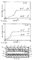
- Figures 12a and 12b show the relationship between the voltage V and the reflectance Rf of the thus formed reflective liquid crystal display panel in the case of having the convex portions 14 shown in Figures 4d and 4f, respectively.
- the reflectance Rf was measured under the same conditions as shown in Figure 3, where the reflective liquid crystal display panel was placed at the position of the model 1.
- the voltage V represents a voltage applied between the pixel electrodes 23 and the reflective film 16, and the reflectance Rf represents a reflectance of an incident ray introduced at an incident angle ⁇ of 30°.
- the reflectance Rf is obtained by calculating a ratio of the intensity of a scattering ray from the reflective liquid crystal display panel as the object for measuring in the direction of the normal thereof to that of a scattering ray from a standard white plate in the direction of the normal thereof.
- the reflectances of the former are higher than those of the latter, respectively, reaching as high as 50%.
- the contrast ratio of the display device of this example was 15 to 20. Thus, it has been proved that the reflective liquid crystal display device of this example provides a very bright screen.
- the convex portions 14 of the reflector 17 having longitudinal and lateral pitches of 38 to 53 ⁇ m and a height of 4 ⁇ m were used.
- the reflective properties of the liquid crystal display device can be controlled in the same manner as described above with the reflector 17 having convex portions 14 with pitches of 100 ⁇ m or less and a height of 10 ⁇ m or less.
- the reflector 17 covered with the reflective film 16 (not shown) is disposed facing the liquid crystal layer 25 as shown in Figure 11, it is preferable to set the height of the convex portions 14 of the reflector 17 lower than the thickness of the liquid crystal layer 25 and to make the inclined sides of the convex portions 14 gentle so as not to disturb the orientation of the liquid crystal layer 25.
- the material for the resist film 12 used for the reflector 17 is not limited to the product OPFR-800, but any photosensitive resins which can be patterned in a light-exposure process positively or negatively can be used for this purpose.
- Such resins include, for example, OMR-83, OMR-85, ONNR-20, OFPR-2, OFPR-830, OFPR-5000 manufactured by Tokyo Ohka Kogyo Co., Ltd., TF-20, 1300-27, 1400-27 manufactured by Shipley, Photoneys manufactured by Toray, RW101 manufactured by Sekisui Fine Chemical Co., and R101 and R633 manufactured by Nippon Kayaku Co.
- a transparent glass substrate was used for the core substrate 11 of the reflector 17, but a non-transparent substrate such as a Si substrate can be used to achieve the same effect.
- the non-transparent substrate has an advantage of being able to integrate circuits on the substrate.
- the reflective film 16 of the reflector 17 faces the liquid crystal layer 25, reducing the distance between the reflective film 16 and the liquid crystal layer 25 and thereby reducing the parallax so as to give a quality display image. Further, the reflective film 16 functions as a counter electrode for the pixel electrodes 23 of the active matrix substrate 20, thereby realizing the simple structure of the liquid crystal display panel and the easy manufacture thereof.
- a color filter 37 can be disposed corresponding to each pixel electrode 23 of the active matrix substrate 20 and a black mask 38 between the adjacent color filters 37, so as to realize a reflective color liquid crystal display panel.
- An effective color display can be obtained by using the above structure of this example, that is, disposing the reflector 17 opposed to the active matrix substrate 20 having the aligning layer 24.
- phase-change guest-host mode such as a light absorption mode like a two-layer guest-host mode, a light scattering mode like a polymer dispersing LCD, or a birefringent display mode used for a ferroelectric LCD.
Abstract
Description
- The present invention relates to a reflective liquid crystal display device which does not need a backlight, and a method for manufacturing the same.
- In recent years, applications of liquid crystal display devices to word processors, lap-top personal computers, pocket-size TV displays, and the like have been in rapid progress. Especially, a reflective liquid crystal display device in which incident light is reflected to effect a display eliminates the necessity of any backlight, thereby lowering power consumption as well as reducing the size and the weight of the device.
- The conventional liquid crystal display devices mostly employ a twisted nematic (TN) mode or a super-twisted nematic (STN) mode. In such display devices, about a half of the natural light introduced therein is absorbed, not being reflected to the outside by a linear polarizer disposed therein, resulting in a dark display. To overcome this trouble, other display modes have been proposed in an attempt to utilize all of the natural light. One example of these is a phase-change guest-host mode (D.L. White and G.N. Taylor, J. Appl. Phys. 45, p. 4718, 1974), which uses a cholesteric-nematic phase transition effect caused by the electric field. A reflective multicolor display using this display mode in combination with microcolor filters has also been proposed (T. Koizumi and T. Uchida, Proceedings of the SID, vol. 29, p. 157, 1988).
- In the liquid crystal display device using the above display mode which does not need the polarizer, a brighter display can be obtained if the intensity of the light scattered in the direction vertical to the display screen is increased for all incident light from every direction. For this purpose, the shape of the filmed surface of a reflector for the display device should be controlled so that optimal reflective properties can be obtaIned. The aforementioned paper by T. Koizumi, et al. discloses a reflector which is fabricated by roughening the surface of a glass substrate with an abrasive, etching the surface with hydrofluoric acid for different periods of time thus controlling the roughness thereof and depositing a silver film on the roughened surface, so as to provide a bright reflective liquid crystal display.
- However, the roughened surface of the above reflector which is formed by scratching the glass substrate with the abrasive is neither uniform in shape nor reproducible. Therefore, in the above disclosed method, it is not possible to obtain a controlled uniform reproducible surface roughness on the reflector, and thus to achieve a reflective liquid crystal display device with optimal reflective properties.
- The objective of the present invention is to provide a reflective liquid crystal display device which comprises a reflector having an effective, reproducible reflective properties, and a method for fabricating such a display device.
- The reflective liquid crystal display device of this invention, which overcomes the above-discussed and numerous other disadvantages and deficiencies of the prior art, comprises an insulating substrate having a transparent electrode formed thereon, a reflector including a core substrate, a number of small convex portions formed on the core substrate by patterning a photosensitive resin applied to one surface of the core substrate by use of a photomask having a predetermined pattern, and a reflective film covering the surface of the core substrate having the convex portions, and a liquid crystal layer sandwiched between the insulating substrate and the reflector.
- In a preferred embodiment, the surface of the reflector on which the reflective film is formed faces the liquid crystal layer.
- In a preferred embodiment, the reflective film of the reflector functions as a counter electrode for the transparent electrode on the insulating substrate.
- In a preferred embodiment, the convex portions are formed at a pitch of 100 µm or less and have a height of 10 µm or less.
- According to another aspect of the present invention, a method for fabricating a reflective liquid crystal display device having a reflector which includes a core substrate, a number of small convex portions formed on the core substrate and a reflective film covering the surface of the core substrate having the convex portions is provided. The method comprises the steps of patterning a photosensitive resin applied to one surface of a core substrate for the reflector by use of a photomask so as to form a number of small convex portions on the core substrate, heat-treating the core substrate having the convex portions, and forming a reflective film on the surface of the core substrate having the convex portions.
- Thus, in the reflective liquid crystal display device of the present invention, a photosensitive resin applied to one surface of the core substrate of the reflector is patterned so as to form a predetermined shape of the convex portions thereon. In this way, the shape, size, and pitch of the convex portions, and the like can be optimally determined, thereby enabling the control of the reflective properties of the reflector effectively and reproducibly so as to provide a bright screen image of the display device.
- Further, the surface of the reflector coated with the reflective film faces the liquid crystal layer, reducing the distance between the reflecting film and the liquid crystal layer and thereby effecting a reduced parallax. Also, in this case, the reflective film can be used as a counter electrode for the transparent electrode on the insulating substrate.
- This invention may be better understood and its numerous objects and advantages will become apparent to those skilled in the art by reference to the accompanying drawings as follows:
- Figure 1 is a sectional view of a reflector constituting a reflective liquid crystal display device according to the present invention;
- Figures 2a to 2d are sectional views showing the steps for fabricating the reflector of Figure 1;
- Figure 3 is a perspective view showing the measurement of the reflective properties of the reflector of Figure 1;
- Figures 4a to 4f are plan views of convex portions for the reflector of Figure 1;
- Figures 5 to 10 are graphs showing the reflective properties of the reflectors having the shapes of convex portions shown in Figures 4a to 4f, respectively, wherein Figures 5a to 10a show the dependence on an incident angle and Figures 5b to 10b show the dependence on an angle with respect to the coordinate axes on the surface of the reflector;
- Figure 11 is a sectional view of a reflective liquid crystal display panel according to the present invention employing the reflector of Figure 1;
- Figures 12a and 12b are graphs showing the applied voltage-reflectance properties; and
- Figure 13 is a sectional view showing an application of the present invention to a color liquid crystal display device.
- Figure 1 shows a
reflector 17 to be used for a reflective liquid crystal display device of the present invention, and Figures 2a to 2d show the steps for fabricating thereflector 17. The procedure for fabricating thereflector 17 will be described as follows. - As shown in figure 2a, a
resist film 12 made of a photosensitive resin is formed on one surface of aglass core substrate 11 preferably by spinning at a speed of 500 to 3000 r.p.m. In this example, a glass plate (No. 7059 manufactured by Corning) having a thickness of 1.1 mm was used for thecore substrate 11, and the glass plate was coated with a photosensitive resin (OFPR-800 manufactured by Tokyo Ohka Kogyo Co., Ltd.) at a spinning speed of 1000 r.p.m. for 30 seconds so as to obtain theresist film 12 having a thickness of 4 µm. Then, thecore substrate 11 coated with theresist film 12 was prebaked at 90°C for 30 minutes. Next, as shown in Figure 2b, aphotomask 13 having a predetermined pattern was disposed over theresist film 12 and light was radiated through thephotomask 13 to theresist film 12, which was then treated with a developer (for example, a 2.38% solution of NMD-3 manufactured by Tokyo Ohka Kogyo Co., Ltd.) so as to form a number offine convex portions 14 on the surface of thecore substrate 11, as shown in Figure 2c. - The section of the thus formed
convex portions 14 is a square having substantially right angles. However, in order to cover theconvex portions 14 with areflective film 16 of a uniform thickness in a later stage, it is preferable to round the squareconvex portions 14. The inventors have found that theconvex portions 14 can be easily rounded by heat treatment preferably at a temperature in the range of 120 to 250°C, more preferably at 200°C. In this example, the heat treatment was performed at 200°C for 30 minutes so as to obtain the roundconvex portions 14 as shown in Figure 2d. - Then, the surface of the
core substrate 11 with the convex portions formed thereon was covered with areflective film 16 having a uniform thickness as shown in Figure 1. The material for thereflective film 16 can be Al, Ni, Cr, Ag, or other metal, and the thickness thereof is preferably 0.01 to 1.0 µm. In this example, thereflective film 16 was formed by the vacuum evaporation of Ag. In this way, thereflector 17 was formed. - The shape of the
convex portions 14 of thereflector 17 obtained after the heat treatment is round as viewed from the top, as shown in Figure 4a. Other shapes such as an ellipse, a square, a rectangle, and a stripe as shown in Figures 4b to 4f are also possible. A diameter D₁ of theround convex portions 14 shown in Figure 4a is for example 33µm, and a lateral gap T₁ and a longitudinal gap T₂ between theadjacent convex portions 14 are 20 µm, respectively. Lateral and longitudinal distances between the centers of theadjacent convex portions 14 or pitches P₁ and P₂ are 53 µm and 38 µm, respectively. In Figure 4b, the stripe convexportions 14 of one example having a width B₁ of 28 µm are formed with a gap T₃ of 10 µm and a pitch P₃ of 38 µm. In Figure 4c, the stripe convexportions 14 of another example having a width B₂ of 33 µm are formed with a gap T₄ of 5 µm and a pitch P₄ of 38 µm. In Figure 4d, theelliptic convex portions 14 having a length B₃ of 48 µm and a width B₄ of 33 µm are formed with gaps T₅ and T₆ of 5 µm, a lateral pitch P₅ of 53 µm and a longitudinal pitch P₆ of 38 µm. In Figure 4e, the rectangularconvex portions 14 of one example having a length B₅ of 43 µm and a width B₆ of 28 µm are formed with a lateral gap T₇ of 10 µm, a longitudinal gap T₈ of 20 µm, a lateral pitch P₇ of 53 µm and a longitudinal pitch P₈ of 48 µm. In Figure 4f, the rectangularconvex portions 14 of another example having a length B₇ of 48 µm and a width B₈ of 33 µm are formed with gaps T₉ and T₁₀ of 5 µm, a lateral pitch P₉ of 53 µm and a longitudinal pitch P₁₀ of 38 µm. - Figure 3 shows a method for measuring the reflective properties of the reflector fabricated as described above. A
model 1 for measuring the reflectance is formed to imitate the state of thereflector 17 being in contact with a liquid crystal layer when thereflector 17 is disposed in an actual liquid crystal display device. In themodel 1, over thereflector 17 is placed adummy glass substrate 2 having a refractive index of 1.5 which is substantially equal to that of an actual liquid crystal layer, and thereflector 17 and thedummy substrate 2 are sealed to each other with an ultraviolet-hardened adhesive 3. - An
incident ray 5 is introduced into thedummy substrate 2 at an incident angle ϑ with respect to the normal of themodel 1 and at an angle φ with respect to the coordinate axes on the model 1 (wherein when φ = 0° the angle φ corresponds to the Y axis of an XY rectangular coordinate, and when φ = +90° or -90° the angle φ corresponds to the X axis thereof). A photomultimeter 4 is disposed above themodel 1 in the direction of the normal of thereflector 17 passing a point on thereflective film 16 irradiated with theincident ray 5. Under these conditions, a scattering ray 6 reflected by thereflector 17 is detected with the photomultimeter 4. The incident angle ϑ and the angle φ of theincident ray 5 are varied to measure the corresponding scattering ray 6, thereby determining the reflective properties of thereflector 17. It has been confirmed that themodel 1 has the same reflective properties as the actual liquid crystal display device. - The reflective properties of the
reflectors 17 corresponding to the shapes of theconvex portions 14 thereof shown in Figures 4a to 4f are shown in Figures 5a and 5b to 10a and 10b, respectively. In Figures 5a to 10a, the reflective intensity of the light introduced at the incident angle ϑ is expressed as the distance from the origin O in the direction of the incident angle ϑ. Each white dot denotes a result obtained when φ = 0°, and each black dot denotes a result obtained when φ = 90°. The chain-line curve P shows the reflective property measured for a standard white plate (magnesium oxide). In Figures 5b to 10b, the reflective intensity R of the light introduced at an incident angle ϑ of 30° is shown as a function of the angle φ with respect to the coordinate axes on the surface of the reflector. - As is apparent from these figures, the reflective intensity R of the
reflector 17 is high when the sides of theconvex portion 14 of thereflector 17 are linear, and it is especially high when the light is introduced into theconvex portion 14 at the right angle to the linear sizes thereof. On the other hand, when the sides of theconvex portion 14 are curved, the dependence on the angle ϑ is reduced. It is advantageous to make best use of these different reflective properties of light and to vary the shape of theconvex portions 14 of thereflector 17, the ratio of the length to the width of theconvex portions 14, and the pitch of the adjacentconvex portions 14, so as to control the reflective intensity R of thereflector 17 arbitrarily and reproducibly. Thus, in a reflective liquid crystal display device comprising thereflector 17 with which the reflective intensity R can be controlled, rays reflected at a desired angle can be effectively obtained. - Further, it has been confirmed that the inclined angle of the sides of the
convex portion 14 can be freely determined by suitably selecting the material and the thickness of the photosensitive resin for the resistfilm 12 and the temperature for the heat treatment, and in turn, by varying the inclined angle of the sides of theconvex portion 14, the dependence of the reflective intensity R on the incident angle ϑ can be controlled. It has also been confirmed that the rate of the regular reflective elements in the reflected rays can be controlled by varying the percentage of the concave portions between the convex portions in the entire area of the reflector. - A reflective liquid crystal display panel fabricated using the above-described
reflector 17 is shown in Figure 11, in which thereflector 17 and anactive matrix substrate 20 are disposed facing each other with a predetermined space therebetween. The thus formed space is surrounded by aseal 26 to define aliquid crystal layer 25 inside. Theactive matrix substrate 20 has a structure of thin film transistors (TFTs) 22 formed on an insulatingsubstrate 21 made of glass for example andpixel electrodes 23 connected to theTFTs 22. Further, an aligninglayer 24 is formed on the entire surface of theglass substrate 21 so as to cover theTFTs 22 and thepixel electrodes 23. The reflective film 16 (not shown in Figure 11) of thereflector 17 is also covered with an aligninglayer 27. Thereflective film 16 has another function as a counter electrode opposing thepixel electrode 23 on theactive matrix substrate 20 via theliquid crystal layer 25. - In this example, the
seal 26 was formed by printing an adhesive sealing agent containing 7 µm-size spacers around the entire edges of thereflector 17 and theactive matrix substrate 20 by a screen printing method. The space surrounded by theseal 26 is filled with the liquid crystal by vacuum deaeration, so as to form theliquid crystal layer 25. In this example, a guest-host liquid crystal with a black-dye mixture (ZL12327 manufactured by Merk) containing an optically active substance (S811 manufactured by Merk) by 4.5% was used for theliquid crystal layer 25. - Figures 12a and 12b show the relationship between the voltage V and the reflectance Rf of the thus formed reflective liquid crystal display panel in the case of having the
convex portions 14 shown in Figures 4d and 4f, respectively. The reflectance Rf was measured under the same conditions as shown in Figure 3, where the reflective liquid crystal display panel was placed at the position of themodel 1. The voltage V represents a voltage applied between thepixel electrodes 23 and thereflective film 16, and the reflectance Rf represents a reflectance of an incident ray introduced at an incident angle ϑ of 30°. The reflectance Rf is obtained by calculating a ratio of the intensity of a scattering ray from the reflective liquid crystal display panel as the object for measuring in the direction of the normal thereof to that of a scattering ray from a standard white plate in the direction of the normal thereof. In Figures 12a and 12b, the solid-line curves 30 and 31 show the respective properties when the angle φ = 0°, and the dashedline curves 32 and 33 show the respective properties when the angle φ = 90°. The reflectances of the former are higher than those of the latter, respectively, reaching as high as 50%. The contrast ratio of the display device of this example was 15 to 20. Thus, it has been proved that the reflective liquid crystal display device of this example provides a very bright screen. - In this example, the
convex portions 14 of thereflector 17 having longitudinal and lateral pitches of 38 to 53 µm and a height of 4 µm were used. However, it has been confirmed that the reflective properties of the liquid crystal display device can be controlled in the same manner as described above with thereflector 17 havingconvex portions 14 with pitches of 100 µm or less and a height of 10 µm or less. Further, when thereflector 17 covered with the reflective film 16 (not shown) is disposed facing theliquid crystal layer 25 as shown in Figure 11, it is preferable to set the height of theconvex portions 14 of thereflector 17 lower than the thickness of theliquid crystal layer 25 and to make the inclined sides of theconvex portions 14 gentle so as not to disturb the orientation of theliquid crystal layer 25. - The material for the resist
film 12 used for thereflector 17 is not limited to the product OPFR-800, but any photosensitive resins which can be patterned in a light-exposure process positively or negatively can be used for this purpose. Such resins include, for example, OMR-83, OMR-85, ONNR-20, OFPR-2, OFPR-830, OFPR-5000 manufactured by Tokyo Ohka Kogyo Co., Ltd., TF-20, 1300-27, 1400-27 manufactured by Shipley, Photoneys manufactured by Toray, RW101 manufactured by Sekisui Fine Chemical Co., and R101 and R633 manufactured by Nippon Kayaku Co. - A transparent glass substrate was used for the
core substrate 11 of thereflector 17, but a non-transparent substrate such as a Si substrate can be used to achieve the same effect. The non-transparent substrate has an advantage of being able to integrate circuits on the substrate. - In the liquid crystal display panel of this example, the
reflective film 16 of thereflector 17 faces theliquid crystal layer 25, reducing the distance between thereflective film 16 and theliquid crystal layer 25 and thereby reducing the parallax so as to give a quality display image. Further, thereflective film 16 functions as a counter electrode for thepixel electrodes 23 of theactive matrix substrate 20, thereby realizing the simple structure of the liquid crystal display panel and the easy manufacture thereof. - Moreover, as shown in Figure 13, a
color filter 37 can be disposed corresponding to eachpixel electrode 23 of theactive matrix substrate 20 and ablack mask 38 between theadjacent color filters 37, so as to realize a reflective color liquid crystal display panel. An effective color display can be obtained by using the above structure of this example, that is, disposing thereflector 17 opposed to theactive matrix substrate 20 having the aligninglayer 24. Alternatively, it is possible to use the reflective film formed on the convex portions as the pixel electrodes. In this case, the reflective film should be formed in a matrix and electrically connected to theTFTs 22. - It is also possible to employ display modes other than the above-mentioned phase-change guest-host mode, such as a light absorption mode like a two-layer guest-host mode, a light scattering mode like a polymer dispersing LCD, or a birefringent display mode used for a ferroelectric LCD.
- It is understood that various other modifications will be apparent to and can be readily made by those skilled in the art without departing from the scope and spirit of this invention. Accordingly, it is not intended that the scope of the claims appended hereto be limited to the description as set forth herein, but rather that the claims be construed as encompassing all the features of patentable novelty that reside in the present invention, including all features that would be treated as equivalents thereof by those skilled in the art to which this invention pertains.
Claims (7)
- A reflective liquid crystal display device comprising:
an insulating substrate having a transparent electrode formed thereon;
a reflector including a core substrate, a number of small convex portions formed on the core substrate by patterning a photosensitive resin applied to one surface of the core substrate by use of a photomask having a predetermined pattern, and a reflective film covering the surface of the core substrate having the convex portions; and
a liquid crystal layer sandwiched between the insulating substrate and the reflector. - A reflective liquid crystal display device according to claim 1, wherein the surface of the reflector on which the reflective film is formed faces the liquid crystal layer.
- A reflective liquid crystal display device according to claim 2, wherein the reflective film of the reflector functions as a counter electrode for the transparent electrode on the insulating substrate.
- A reflective liquid crystal display device according to claim 1, wherein the convex portions are formed at a pitch of 100 µm or less and have a height of 10 µm or less.
- A reflective liquid crystal display device according to claim 2, wherein the convex portions are formed at a pitch of 100 µm or less and have a height of 10 µm or less.
- A reflective liquid crystal display device according to claim 3, wherein the convex portions are formed at a pitch of 100 µm or less and have a height of 10 µm or less.
- A method for fabricating a reflective liquid crystal display device provided with a reflector including a core substrate, a number of small convex portions formed on the core substrate and a reflective film covering the surface of the core substrate having the convex portions, the method comprising the steps of:
patterning a photosensitive resin applied to one surface of a core substrate for the reflector by use of a photomask so as to form a number of small convex portions on the core substrate;
heat-treating the core substrate having the convex portions; and
forming a reflective film on the surface of the core substrate having the convex portions.
Applications Claiming Priority (2)
| Application Number | Priority Date | Filing Date | Title |
|---|---|---|---|
| JP3004573A JP2698218B2 (en) | 1991-01-18 | 1991-01-18 | Reflective liquid crystal display device and method of manufacturing the same |
| JP4573/91 | 1991-01-18 |
Publications (3)
| Publication Number | Publication Date |
|---|---|
| EP0495679A2 true EP0495679A2 (en) | 1992-07-22 |
| EP0495679A3 EP0495679A3 (en) | 1992-11-19 |
| EP0495679B1 EP0495679B1 (en) | 1996-04-03 |
Family
ID=11587781
Family Applications (1)
| Application Number | Title | Priority Date | Filing Date |
|---|---|---|---|
| EP92300438A Expired - Lifetime EP0495679B1 (en) | 1991-01-18 | 1992-01-17 | A reflective liquid crystal display device and a method for fabricating same |
Country Status (4)
| Country | Link |
|---|---|
| US (1) | US5204765A (en) |
| EP (1) | EP0495679B1 (en) |
| JP (1) | JP2698218B2 (en) |
| DE (1) | DE69209534T2 (en) |
Cited By (16)
| Publication number | Priority date | Publication date | Assignee | Title |
|---|---|---|---|---|
| EP0529672A2 (en) * | 1991-08-30 | 1993-03-03 | Ag Technology Co. Ltd. | Liquid crystal display element and liquid crystal display apparatus using the same |
| EP0549890A1 (en) * | 1991-12-31 | 1993-07-07 | AT&T Corp. | LCD Display with microtextured back reflector and method for making same |
| EP0557110A2 (en) * | 1992-02-19 | 1993-08-25 | Sharp Kabushiki Kaisha | A reflective substrate, a method for producing the same, and a liquid crystal display device using the same |
| EP0586220A1 (en) * | 1992-08-28 | 1994-03-09 | Sharp Kabushiki Kaisha | Reflection type liquid crystal display device |
| EP0617310A1 (en) * | 1993-03-24 | 1994-09-28 | Sharp Kabushiki Kaisha | Reflection type liquid crystal display device and manufacturing method thereof |
| EP0627638A1 (en) * | 1993-06-02 | 1994-12-07 | Hughes Aircraft Company | Elliptical diffuser |
| US6266111B1 (en) * | 1998-03-10 | 2001-07-24 | Sony Corporation | Diffuse reflection plate, manufacturing method thereof, and reflection-type display device |
| WO2002010806A1 (en) * | 2000-07-28 | 2002-02-07 | Matsushita Electric Industrial Co., Ltd. | Reflection sheet and production method therefor, and display unit using it |
| EP1205786A1 (en) * | 2000-11-08 | 2002-05-15 | Nec Corporation | Reflection plate, reflection type liquid crystal display apparatus, and method of manufacturing the same |
| WO2002048756A1 (en) * | 2000-12-14 | 2002-06-20 | Mitsui Chemicals Inc. | Reflector, sidelight type backlighting apparatus and reflector substrate |
| EP1231487A1 (en) * | 1999-10-21 | 2002-08-14 | Matsushita Electric Industrial Co., Ltd. | Reflecting plate, method for manufacturing the same, display element, and display device |
| WO2003032025A2 (en) * | 2001-10-04 | 2003-04-17 | Koninklijke Philips Electronics N.V. | Optical reflector and display device using it |
| WO2003046650A1 (en) * | 2001-11-29 | 2003-06-05 | Koninklijke Philips Electronics N.V. | A diffuse reflector for a liquid crystal display device |
| WO2004055582A1 (en) * | 2002-12-17 | 2004-07-01 | Koninklijke Philips Electronics N.V. | Liquid crystal display device with an anisotropically reflecting layer and manufacturing method for the same |
| EP1237016A3 (en) * | 2001-02-28 | 2005-01-12 | NEC LCD Technologies, Ltd. | Reflector and reflection-type LCD device using the same |
| WO2022134029A1 (en) * | 2020-12-25 | 2022-06-30 | 京东方科技集团股份有限公司 | Display panel, method for manufacturing display panel, and display device |
Families Citing this family (88)
| Publication number | Priority date | Publication date | Assignee | Title |
|---|---|---|---|---|
| EP0536898B1 (en) * | 1991-09-10 | 1997-07-02 | Sharp Kabushiki Kaisha | Reflection type liquid crystal display device and method of manufacturing the same |
| JPH0667173A (en) * | 1992-08-19 | 1994-03-11 | Sharp Corp | Liquid crystal display device |
| JP3358744B2 (en) * | 1993-05-06 | 2002-12-24 | シャープ株式会社 | Liquid crystal display |
| US5691791A (en) * | 1993-07-30 | 1997-11-25 | Sharp Kabushiki Kaisha | Reflective liquid crystal display device and reflector |
| JPH0784252A (en) * | 1993-09-16 | 1995-03-31 | Sharp Corp | Liquid crystal display device |
| MY114271A (en) * | 1994-05-12 | 2002-09-30 | Casio Computer Co Ltd | Reflection type color liquid crystal display device |
| US5550663A (en) * | 1994-05-24 | 1996-08-27 | Omron Corporation | Method of manufacturing optical low-pass filter |
| US5610741A (en) * | 1994-06-24 | 1997-03-11 | Sharp Kabushiki Kaisha | Reflection type liquid crystal display device with bumps on the reflector |
| JP2888177B2 (en) * | 1994-09-28 | 1999-05-10 | 日本電気株式会社 | Liquid crystal display |
| JPH08166605A (en) * | 1994-10-14 | 1996-06-25 | Sharp Corp | Liquid crystal display device |
| KR100207135B1 (en) * | 1994-10-18 | 1999-07-15 | 니시무로 타이죠 | Reflection type liquid crystal display device and method of manufacturing the same |
| JP2912176B2 (en) * | 1994-12-28 | 1999-06-28 | 日本電気株式会社 | Reflective liquid crystal display |
| US5626800A (en) * | 1995-02-03 | 1997-05-06 | Minnesota Mining And Manufacturing Company | Prevention of groove tip deformation in brightness enhancement film |
| JP2768313B2 (en) | 1995-06-13 | 1998-06-25 | 日本電気株式会社 | Reflective liquid crystal display |
| US6097458A (en) * | 1995-12-11 | 2000-08-01 | Sharp Kabushiki Kaisha | Reflector, reflective liquid crystal display incorporating the same and method for fabricating the same |
| US5714247A (en) * | 1996-06-14 | 1998-02-03 | Industrial Technology Research Institute | Reflective surface for LCD and method for forming it |
| US5595790A (en) * | 1996-06-21 | 1997-01-21 | Industrial Technology Research Institute | Method for forming a reflective surface for a LCD |
| JP3213242B2 (en) | 1996-10-23 | 2001-10-02 | シャープ株式会社 | Reflection plate, reflection type liquid crystal display device and method of manufacturing the same |
| JP3694138B2 (en) | 1997-02-20 | 2005-09-14 | アルプス電気株式会社 | Reflector manufacturing method and liquid crystal display device including the reflector |
| JP3270821B2 (en) * | 1997-03-12 | 2002-04-02 | シャープ株式会社 | Reflective liquid crystal display device and method of manufacturing the same |
| US5949510A (en) * | 1997-09-12 | 1999-09-07 | Industrial Technology Research Institute | Method for making wide viewing angle LCD and devices made |
| JP3522517B2 (en) * | 1997-12-22 | 2004-04-26 | シャープ株式会社 | Manufacturing method of reflector |
| US6295109B1 (en) * | 1997-12-26 | 2001-09-25 | Sharp Kabushiki Kaisha | LCD with plurality of pixels having reflective and transmissive regions |
| US6304309B1 (en) | 1998-03-19 | 2001-10-16 | Matsushita Electric Industrial Co., Ltd. | Liquid crystal display device and method of manufacturing the same |
| US6108131A (en) | 1998-05-14 | 2000-08-22 | Moxtek | Polarizer apparatus for producing a generally polarized beam of light |
| KR100463598B1 (en) * | 1998-05-15 | 2005-05-16 | 엘지.필립스 엘시디 주식회사 | A reflective-type liquid crystal display device and a reflector thereof |
| JP4292596B2 (en) * | 1998-06-19 | 2009-07-08 | ソニー株式会社 | Diffuse reflector, manufacturing method thereof and display device |
| US6081376A (en) * | 1998-07-16 | 2000-06-27 | Moxtek | Reflective optical polarizer device with controlled light distribution and liquid crystal display incorporating the same |
| JP2000047200A (en) | 1998-07-31 | 2000-02-18 | Hitachi Ltd | Diffusive reflector, liquid crystal display device using that, and its production |
| KR100306546B1 (en) * | 1998-09-28 | 2001-11-02 | 마찌다 가쯔히꼬 | Method of manufacturing liquid crystal display apparatus |
| KR100546703B1 (en) * | 1998-12-11 | 2006-03-23 | 엘지.필립스 엘시디 주식회사 | Reflecting Substrate of Reflective Type Liquid Crystal Display Devices |
| KR100507270B1 (en) * | 1999-06-29 | 2005-08-10 | 비오이 하이디스 테크놀로지 주식회사 | Method for forming topology in reflective LCD |
| JP3091190B1 (en) | 1999-06-30 | 2000-09-25 | 京セラ株式会社 | Transflective liquid crystal display |
| KR100407413B1 (en) | 1999-07-19 | 2003-11-28 | 마쯔시다덴기산교 가부시키가이샤 | Reflector, method of fabricating the same, reflective display device comprising reflector, and method of fabricating the same |
| US6447120B2 (en) | 1999-07-28 | 2002-09-10 | Moxtex | Image projection system with a polarizing beam splitter |
| US6666556B2 (en) | 1999-07-28 | 2003-12-23 | Moxtek, Inc | Image projection system with a polarizing beam splitter |
| US7306338B2 (en) * | 1999-07-28 | 2007-12-11 | Moxtek, Inc | Image projection system with a polarizing beam splitter |
| JP3501698B2 (en) | 1999-10-18 | 2004-03-02 | Nec液晶テクノロジー株式会社 | Reflective color liquid crystal display device and method of manufacturing the same |
| WO2001061383A1 (en) * | 2000-02-16 | 2001-08-23 | Matsushita Electric Industrial Co., Ltd. | Irregular-shape body, reflection sheet and reflection-type liquid crystal display element , and production method and production device therefor |
| US6791015B2 (en) * | 2000-10-30 | 2004-09-14 | E. I. Du Pont De Nemours And Company | Fructan biosynthetic enzymes |
| JP4993830B2 (en) * | 2000-11-11 | 2012-08-08 | 三星電子株式会社 | Reflective liquid crystal display device and manufacturing method thereof |
| US6335150B1 (en) * | 2000-12-05 | 2002-01-01 | Wintek Corporation | Manufacturing method for reflecting panel of reflective liquid crystal display |
| US7375887B2 (en) | 2001-03-27 | 2008-05-20 | Moxtek, Inc. | Method and apparatus for correcting a visible light beam using a wire-grid polarizer |
| JP3753673B2 (en) * | 2001-06-20 | 2006-03-08 | セイコーエプソン株式会社 | Manufacturing method of liquid crystal display device |
| JP4718725B2 (en) * | 2001-07-03 | 2011-07-06 | Nec液晶テクノロジー株式会社 | Manufacturing method of liquid crystal display device |
| TW574532B (en) * | 2001-07-18 | 2004-02-01 | Au Optronics Corp | Method for manufacturing reflective TFT LCD devices with coarse diffusing surfaces |
| KR100757789B1 (en) * | 2001-08-06 | 2007-09-11 | 삼성전자주식회사 | Reflective type liquid crystal device |
| JP3842604B2 (en) * | 2001-09-21 | 2006-11-08 | 株式会社日立製作所 | Liquid crystal display |
| US20050179838A1 (en) * | 2001-09-28 | 2005-08-18 | Yoshihiko Hamawaki | Reflecting electrode forming method and liquid crystal display |
| US6909473B2 (en) * | 2002-01-07 | 2005-06-21 | Eastman Kodak Company | Display apparatus and method |
| US7061561B2 (en) * | 2002-01-07 | 2006-06-13 | Moxtek, Inc. | System for creating a patterned polarization compensator |
| TWI227340B (en) * | 2002-02-25 | 2005-02-01 | Himax Tech Inc | Color filter and liquid crystal display |
| US6785050B2 (en) | 2002-05-09 | 2004-08-31 | Moxtek, Inc. | Corrosion resistant wire-grid polarizer and method of fabrication |
| KR100863164B1 (en) * | 2002-05-17 | 2008-10-13 | 옵트렉스 가부시키가이샤 | Light reflective structure, method for producing the same and display |
| KR100484953B1 (en) * | 2002-08-12 | 2005-04-22 | 엘지.필립스 엘시디 주식회사 | reflective electrode of reflection or transflective type LCD and fabrication method of thereof |
| TWI300866B (en) * | 2002-08-30 | 2008-09-11 | Au Optronics Corp | |
| US7088404B2 (en) * | 2002-12-12 | 2006-08-08 | Seiko Epson Corporation | Substrate for electro-optical device having particular concave portions and convex portions and flat section on the surface of a base layer |
| US6894748B2 (en) * | 2003-06-02 | 2005-05-17 | Wintek Corporation | Bump structure of a scattering reflective board and method for manufacturing the bump structure |
| KR100989166B1 (en) * | 2003-08-22 | 2010-10-20 | 엘지디스플레이 주식회사 | Liquid Crystal Display Device And Method For Fabricating The Same |
| US7388635B2 (en) | 2004-11-26 | 2008-06-17 | Kyocera Corporation | Liquid crystal display device and display equipment using the same |
| JP4663302B2 (en) * | 2004-11-26 | 2011-04-06 | 京セラ株式会社 | Liquid crystal display device and display body using the same |
| US7570424B2 (en) * | 2004-12-06 | 2009-08-04 | Moxtek, Inc. | Multilayer wire-grid polarizer |
| US7961393B2 (en) | 2004-12-06 | 2011-06-14 | Moxtek, Inc. | Selectively absorptive wire-grid polarizer |
| US20080055722A1 (en) * | 2006-08-31 | 2008-03-06 | Perkins Raymond T | Optical Polarization Beam Combiner/Splitter with an Inorganic, Dielectric Grid Polarizer |
| US20080055721A1 (en) * | 2006-08-31 | 2008-03-06 | Perkins Raymond T | Light Recycling System with an Inorganic, Dielectric Grid Polarizer |
| US7800823B2 (en) * | 2004-12-06 | 2010-09-21 | Moxtek, Inc. | Polarization device to polarize and further control light |
| US20080055720A1 (en) * | 2006-08-31 | 2008-03-06 | Perkins Raymond T | Optical Data Storage System with an Inorganic, Dielectric Grid Polarizer |
| US7630133B2 (en) * | 2004-12-06 | 2009-12-08 | Moxtek, Inc. | Inorganic, dielectric, grid polarizer and non-zero order diffraction grating |
| US20080055549A1 (en) * | 2006-08-31 | 2008-03-06 | Perkins Raymond T | Projection Display with an Inorganic, Dielectric Grid Polarizer |
| JP4480599B2 (en) | 2005-02-14 | 2010-06-16 | Nec液晶テクノロジー株式会社 | Reflector, method for manufacturing the same, and liquid crystal display device |
| US20070296921A1 (en) * | 2006-06-26 | 2007-12-27 | Bin Wang | Projection display with a cube wire-grid polarizing beam splitter |
| US20070297052A1 (en) * | 2006-06-26 | 2007-12-27 | Bin Wang | Cube wire-grid polarizing beam splitter |
| JP4883525B2 (en) | 2006-08-02 | 2012-02-22 | Nltテクノロジー株式会社 | Reflector and liquid crystal display device |
| US8755113B2 (en) * | 2006-08-31 | 2014-06-17 | Moxtek, Inc. | Durable, inorganic, absorptive, ultra-violet, grid polarizer |
| JP2008165385A (en) * | 2006-12-27 | 2008-07-17 | Dainippon Printing Co Ltd | Infrared reflection pattern print transparent sheet |
| US7789515B2 (en) * | 2007-05-17 | 2010-09-07 | Moxtek, Inc. | Projection device with a folded optical path and wire-grid polarizer |
| US20080316599A1 (en) * | 2007-06-22 | 2008-12-25 | Bin Wang | Reflection-Repressed Wire-Grid Polarizer |
| JP2007310407A (en) * | 2007-06-27 | 2007-11-29 | Sony Corp | Method for manufacturing light reflecting plate, and display device |
| JP4872983B2 (en) * | 2008-08-04 | 2012-02-08 | ソニー株式会社 | Diffuse reflector and display device |
| US8248696B2 (en) | 2009-06-25 | 2012-08-21 | Moxtek, Inc. | Nano fractal diffuser |
| US8913321B2 (en) | 2010-09-21 | 2014-12-16 | Moxtek, Inc. | Fine pitch grid polarizer |
| US8611007B2 (en) | 2010-09-21 | 2013-12-17 | Moxtek, Inc. | Fine pitch wire grid polarizer |
| US8913320B2 (en) | 2011-05-17 | 2014-12-16 | Moxtek, Inc. | Wire grid polarizer with bordered sections |
| US8873144B2 (en) | 2011-05-17 | 2014-10-28 | Moxtek, Inc. | Wire grid polarizer with multiple functionality sections |
| US8922890B2 (en) | 2012-03-21 | 2014-12-30 | Moxtek, Inc. | Polarizer edge rib modification |
| KR20140066449A (en) * | 2012-11-23 | 2014-06-02 | 삼성디스플레이 주식회사 | Reflect sheet, backlight unit, liquid crystal display device and manufacturing method thereof |
| US9354374B2 (en) | 2013-10-24 | 2016-05-31 | Moxtek, Inc. | Polarizer with wire pair over rib |
| TWI704411B (en) | 2017-04-25 | 2020-09-11 | 友達光電股份有限公司 | Photo mask, corresponding spacer structure and liquid crystal panel using the same |
Citations (4)
| Publication number | Priority date | Publication date | Assignee | Title |
|---|---|---|---|---|
| EP0084930A1 (en) * | 1982-01-21 | 1983-08-03 | Kabushiki Kaisha Toshiba | Liquid crystal display device |
| US4431272A (en) * | 1980-05-08 | 1984-02-14 | Kabushiki Kaisha Suwa Seikosha | Liquid crystal display device |
| JPH0283525A (en) * | 1988-09-21 | 1990-03-23 | Seiko Epson Corp | Production of lens array |
| JPH02244003A (en) * | 1989-03-16 | 1990-09-28 | Nec Corp | Reflection type grating lens and production thereof |
Family Cites Families (10)
| Publication number | Priority date | Publication date | Assignee | Title |
|---|---|---|---|---|
| CH589306A5 (en) * | 1975-06-27 | 1977-06-30 | Bbc Brown Boveri & Cie | |
| US4456336A (en) * | 1981-10-06 | 1984-06-26 | Minnesota Mining And Manufacturing Company | High brightness internal reflector for liquid crystal displays and its method of fabrication |
| JPH0762747B2 (en) * | 1984-10-25 | 1995-07-05 | 帝人株式会社 | Base film for liquid crystal display reflector |
| JPS61128279A (en) * | 1984-11-27 | 1986-06-16 | 帝人株式会社 | Liquid crystal display reflector |
| JPS62153935A (en) * | 1985-12-27 | 1987-07-08 | Canon Inc | Scanning optical device |
| JPS62153902A (en) * | 1985-12-27 | 1987-07-08 | Matsushita Electric Ind Co Ltd | Production of color filter for liquid crystal display body |
| JPS63249802A (en) * | 1987-04-07 | 1988-10-17 | Toshiba Corp | Production of color filter |
| FR2623649B1 (en) * | 1987-11-23 | 1992-05-15 | Asulab Sa | LIQUID CRYSTAL DISPLAY CELL |
| US5076668A (en) * | 1988-01-25 | 1991-12-31 | Taliq Corporation | Gain reflector-liquid crystal display |
| JP2924055B2 (en) * | 1989-12-08 | 1999-07-26 | セイコーエプソン株式会社 | Reflective liquid crystal display |
-
1991
- 1991-01-18 JP JP3004573A patent/JP2698218B2/en not_active Expired - Lifetime
-
1992
- 1992-01-17 DE DE69209534T patent/DE69209534T2/en not_active Expired - Lifetime
- 1992-01-17 EP EP92300438A patent/EP0495679B1/en not_active Expired - Lifetime
- 1992-01-17 US US07/822,300 patent/US5204765A/en not_active Expired - Lifetime
Patent Citations (4)
| Publication number | Priority date | Publication date | Assignee | Title |
|---|---|---|---|---|
| US4431272A (en) * | 1980-05-08 | 1984-02-14 | Kabushiki Kaisha Suwa Seikosha | Liquid crystal display device |
| EP0084930A1 (en) * | 1982-01-21 | 1983-08-03 | Kabushiki Kaisha Toshiba | Liquid crystal display device |
| JPH0283525A (en) * | 1988-09-21 | 1990-03-23 | Seiko Epson Corp | Production of lens array |
| JPH02244003A (en) * | 1989-03-16 | 1990-09-28 | Nec Corp | Reflection type grating lens and production thereof |
Non-Patent Citations (3)
| Title |
|---|
| PATENT ABSTRACTS OF JAPAN vol. 14, no. 283 (P-1063)19 June 1990 & JP-A-2 083 525 ( SEIKO ) 23 March 1990 * |
| PATENT ABSTRACTS OF JAPAN vol. 14, no. 565 (P-1143)17 December 1990 & JP-A-2 244 003 ( NEC ) 28 September 1990 * |
| PROCEEDINGS OF THE SID. vol. 29, no. 2, 1988, LOS ANGELES US pages 157 - 160; T. KOIZUMI ET AL.: 'Reflective Multicolor LCD (II): improvement in the brightness' * |
Cited By (31)
| Publication number | Priority date | Publication date | Assignee | Title |
|---|---|---|---|---|
| EP0529672A3 (en) * | 1991-08-30 | 1993-09-22 | Ag Technology Co. Ltd. | Liquid crystal display element and liquid crystal display apparatus using the same |
| EP0529672A2 (en) * | 1991-08-30 | 1993-03-03 | Ag Technology Co. Ltd. | Liquid crystal display element and liquid crystal display apparatus using the same |
| EP0549890A1 (en) * | 1991-12-31 | 1993-07-07 | AT&T Corp. | LCD Display with microtextured back reflector and method for making same |
| EP0557110A2 (en) * | 1992-02-19 | 1993-08-25 | Sharp Kabushiki Kaisha | A reflective substrate, a method for producing the same, and a liquid crystal display device using the same |
| EP0557110A3 (en) * | 1992-02-19 | 1993-11-24 | Sharp Kk | A reflective substrate, a method for producing the same, and a liquid crystal display device using the same |
| EP0586220A1 (en) * | 1992-08-28 | 1994-03-09 | Sharp Kabushiki Kaisha | Reflection type liquid crystal display device |
| US5526149A (en) * | 1992-08-28 | 1996-06-11 | Sharp Kabushiki Kaisha | Reflection type liquid crystal display device |
| US5500750A (en) * | 1993-03-24 | 1996-03-19 | Sharp Kabushiki Kaisha | Manufacturing method of reflection type liquid crystal display devices having light shield elements and reflective electrodes formed of same material |
| EP0617310A1 (en) * | 1993-03-24 | 1994-09-28 | Sharp Kabushiki Kaisha | Reflection type liquid crystal display device and manufacturing method thereof |
| US5473454A (en) * | 1993-06-02 | 1995-12-05 | Hughes Aircraft Company | Elliptical diffuser |
| EP0627638A1 (en) * | 1993-06-02 | 1994-12-07 | Hughes Aircraft Company | Elliptical diffuser |
| US6266111B1 (en) * | 1998-03-10 | 2001-07-24 | Sony Corporation | Diffuse reflection plate, manufacturing method thereof, and reflection-type display device |
| US6781759B1 (en) | 1999-10-21 | 2004-08-24 | Matsushita Electric Industrial Co., Ltd. | Reflector, production method thereof, display element, and display device |
| EP1231487A1 (en) * | 1999-10-21 | 2002-08-14 | Matsushita Electric Industrial Co., Ltd. | Reflecting plate, method for manufacturing the same, display element, and display device |
| EP1231487A4 (en) * | 1999-10-21 | 2003-06-04 | Matsushita Electric Ind Co Ltd | Reflecting plate, method for manufacturing the same, display element, and display device |
| WO2002010806A1 (en) * | 2000-07-28 | 2002-02-07 | Matsushita Electric Industrial Co., Ltd. | Reflection sheet and production method therefor, and display unit using it |
| US7215393B2 (en) | 2000-07-28 | 2007-05-08 | Matsushita Electric Industrial Co., Ltd. | Reflective plate and display device using the plate |
| EP1205786A1 (en) * | 2000-11-08 | 2002-05-15 | Nec Corporation | Reflection plate, reflection type liquid crystal display apparatus, and method of manufacturing the same |
| US6943856B2 (en) | 2000-11-08 | 2005-09-13 | Nec Corporation | Reflection plate, reflection type liquid crystal display apparatus, and method of manufacturing the same |
| WO2002048756A1 (en) * | 2000-12-14 | 2002-06-20 | Mitsui Chemicals Inc. | Reflector, sidelight type backlighting apparatus and reflector substrate |
| US6683720B2 (en) | 2000-12-14 | 2004-01-27 | Mitsui Chemicals, Inc. | Reflector, sidelight type backlighting apparatus and reflector substrate |
| EP1237016A3 (en) * | 2001-02-28 | 2005-01-12 | NEC LCD Technologies, Ltd. | Reflector and reflection-type LCD device using the same |
| US7092051B2 (en) | 2001-02-28 | 2006-08-15 | Nec Lcd Technologies, Ltd. | Reflection-type LCD device using the same |
| US7196755B2 (en) | 2001-02-28 | 2007-03-27 | Nec Lcd Technologies, Ltd. | Reflector and reflection-type LCD device using the same |
| WO2003032025A3 (en) * | 2001-10-04 | 2003-10-23 | Koninkl Philips Electronics Nv | Optical reflector and display device using it |
| WO2003032025A2 (en) * | 2001-10-04 | 2003-04-17 | Koninklijke Philips Electronics N.V. | Optical reflector and display device using it |
| WO2003046650A1 (en) * | 2001-11-29 | 2003-06-05 | Koninklijke Philips Electronics N.V. | A diffuse reflector for a liquid crystal display device |
| US7543950B2 (en) | 2001-11-29 | 2009-06-09 | Tpo Hong Kong Holding Limited | Diffuse reflector for a liquid crystal display device |
| KR100911959B1 (en) * | 2001-11-29 | 2009-08-13 | 티피오 홍콩 홀딩 리미티드 | A method of forming a reflector member, a reflective structure and liquid crystal display device |
| WO2004055582A1 (en) * | 2002-12-17 | 2004-07-01 | Koninklijke Philips Electronics N.V. | Liquid crystal display device with an anisotropically reflecting layer and manufacturing method for the same |
| WO2022134029A1 (en) * | 2020-12-25 | 2022-06-30 | 京东方科技集团股份有限公司 | Display panel, method for manufacturing display panel, and display device |
Also Published As
| Publication number | Publication date |
|---|---|
| EP0495679A3 (en) | 1992-11-19 |
| US5204765A (en) | 1993-04-20 |
| JPH04243226A (en) | 1992-08-31 |
| EP0495679B1 (en) | 1996-04-03 |
| DE69209534D1 (en) | 1996-05-09 |
| JP2698218B2 (en) | 1998-01-19 |
| DE69209534T2 (en) | 1996-09-19 |
Similar Documents
| Publication | Publication Date | Title |
|---|---|---|
| EP0495679B1 (en) | A reflective liquid crystal display device and a method for fabricating same | |
| EP0557110B1 (en) | A reflective substrate, a method for producing the same, and a liquid crystal display device using the same | |
| EP0467659B1 (en) | A reflective-type liquid crystal display device and method for producing same | |
| US5714247A (en) | Reflective surface for LCD and method for forming it | |
| JP3066192B2 (en) | Method for manufacturing reflective active matrix substrate | |
| EP0586220A1 (en) | Reflection type liquid crystal display device | |
| EP0536898A1 (en) | Reflection type liquid crystal display device and method of manufacturing the same | |
| JPH0784252A (en) | Liquid crystal display device | |
| KR19980024738A (en) | Diffusion light guide plate, backlight source and liquid crystal display device using the same | |
| JPH07333598A (en) | Liquid crystal display device | |
| JP2003172926A (en) | Liquid crystal display device and electronic appliance | |
| WO2001051985A1 (en) | Lcd, method of manufacture thereof, and electronic device | |
| KR100421902B1 (en) | Reflective Liquid Crystal Display | |
| US20020118324A1 (en) | Substrate for a liquid crystal device, method of manufacturing a substrate for a liquid crystal device, a liquid crystal device, a method of manufacturing a liquid crystal device , and an electronic apparatus | |
| JPH07333612A (en) | Liquid crystal display device | |
| JP2740401B2 (en) | Reflective liquid crystal display device and method of manufacturing the same | |
| US7423711B2 (en) | Display apparatus | |
| GB2064805A (en) | Liquid crystal display device | |
| JPH04308816A (en) | Reflection type liquid crystal display device and production thereof | |
| US5595790A (en) | Method for forming a reflective surface for a LCD | |
| JPH052235B2 (en) | ||
| JPH112718A (en) | Color filter and color liquid crystal display device | |
| JPH07294921A (en) | Liquid crystal display device | |
| JPH09258219A (en) | Liquid crystal display device | |
| KR100460060B1 (en) | Reflective substrate, its manufacturing method and reflective liquid crystal display device |
Legal Events
| Date | Code | Title | Description |
|---|---|---|---|
| PUAI | Public reference made under article 153(3) epc to a published international application that has entered the european phase |
Free format text: ORIGINAL CODE: 0009012 |
|
| AK | Designated contracting states |
Kind code of ref document: A2 Designated state(s): DE FR GB NL |
|
| RIN1 | Information on inventor provided before grant (corrected) |
Inventor name: KIMURA, NAOFUMI Inventor name: ISHII, YUTAKA Inventor name: SEIICHI, MITSUI |
|
| PUAL | Search report despatched |
Free format text: ORIGINAL CODE: 0009013 |
|
| AK | Designated contracting states |
Kind code of ref document: A3 Designated state(s): DE FR GB NL |
|
| 17P | Request for examination filed |
Effective date: 19930302 |
|
| 17Q | First examination report despatched |
Effective date: 19940706 |
|
| GRAA | (expected) grant |
Free format text: ORIGINAL CODE: 0009210 |
|
| AK | Designated contracting states |
Kind code of ref document: B1 Designated state(s): DE FR GB NL |
|
| REF | Corresponds to: |
Ref document number: 69209534 Country of ref document: DE Date of ref document: 19960509 |
|
| ET | Fr: translation filed | ||
| GRAH | Despatch of communication of intention to grant a patent |
Free format text: ORIGINAL CODE: EPIDOS IGRA |
|
| PLBE | No opposition filed within time limit |
Free format text: ORIGINAL CODE: 0009261 |
|
| STAA | Information on the status of an ep patent application or granted ep patent |
Free format text: STATUS: NO OPPOSITION FILED WITHIN TIME LIMIT |
|
| 26N | No opposition filed | ||
| REG | Reference to a national code |
Ref country code: GB Ref legal event code: IF02 |
|
| PGFP | Annual fee paid to national office [announced via postgrant information from national office to epo] |
Ref country code: NL Payment date: 20110120 Year of fee payment: 20 Ref country code: FR Payment date: 20110128 Year of fee payment: 20 Ref country code: DE Payment date: 20110112 Year of fee payment: 20 |
|
| PGFP | Annual fee paid to national office [announced via postgrant information from national office to epo] |
Ref country code: GB Payment date: 20110112 Year of fee payment: 20 |
|
| REG | Reference to a national code |
Ref country code: DE Ref legal event code: R071 Ref document number: 69209534 Country of ref document: DE |
|
| REG | Reference to a national code |
Ref country code: DE Ref legal event code: R071 Ref document number: 69209534 Country of ref document: DE |
|
| REG | Reference to a national code |
Ref country code: NL Ref legal event code: V4 Effective date: 20120117 |
|
| REG | Reference to a national code |
Ref country code: GB Ref legal event code: PE20 Expiry date: 20120116 |
|
| PG25 | Lapsed in a contracting state [announced via postgrant information from national office to epo] |
Ref country code: DE Free format text: LAPSE BECAUSE OF EXPIRATION OF PROTECTION Effective date: 20120118 |
|
| PG25 | Lapsed in a contracting state [announced via postgrant information from national office to epo] |
Ref country code: GB Free format text: LAPSE BECAUSE OF EXPIRATION OF PROTECTION Effective date: 20120116 |