EP0502425A2 - Magneto-optical recording medium - Google Patents
Magneto-optical recording medium Download PDFInfo
- Publication number
- EP0502425A2 EP0502425A2 EP92103365A EP92103365A EP0502425A2 EP 0502425 A2 EP0502425 A2 EP 0502425A2 EP 92103365 A EP92103365 A EP 92103365A EP 92103365 A EP92103365 A EP 92103365A EP 0502425 A2 EP0502425 A2 EP 0502425A2
- Authority
- EP
- European Patent Office
- Prior art keywords
- layer
- magneto
- rare earth
- recording medium
- film
- Prior art date
- Legal status (The legal status is an assumption and is not a legal conclusion. Google has not performed a legal analysis and makes no representation as to the accuracy of the status listed.)
- Granted
Links
Images

Classifications
-
- G—PHYSICS
- G11—INFORMATION STORAGE
- G11B—INFORMATION STORAGE BASED ON RELATIVE MOVEMENT BETWEEN RECORD CARRIER AND TRANSDUCER
- G11B11/00—Recording on or reproducing from the same record carrier wherein for these two operations the methods are covered by different main groups of groups G11B3/00 - G11B7/00 or by different subgroups of group G11B9/00; Record carriers therefor
- G11B11/10—Recording on or reproducing from the same record carrier wherein for these two operations the methods are covered by different main groups of groups G11B3/00 - G11B7/00 or by different subgroups of group G11B9/00; Record carriers therefor using recording by magnetic means or other means for magnetisation or demagnetisation of a record carrier, e.g. light induced spin magnetisation; Demagnetisation by thermal or stress means in the presence or not of an orienting magnetic field
- G11B11/105—Recording on or reproducing from the same record carrier wherein for these two operations the methods are covered by different main groups of groups G11B3/00 - G11B7/00 or by different subgroups of group G11B9/00; Record carriers therefor using recording by magnetic means or other means for magnetisation or demagnetisation of a record carrier, e.g. light induced spin magnetisation; Demagnetisation by thermal or stress means in the presence or not of an orienting magnetic field using a beam of light or a magnetic field for recording by change of magnetisation and a beam of light for reproducing, i.e. magneto-optical, e.g. light-induced thermomagnetic recording, spin magnetisation recording, Kerr or Faraday effect reproducing
- G11B11/10582—Record carriers characterised by the selection of the material or by the structure or form
- G11B11/10586—Record carriers characterised by the selection of the material or by the structure or form characterised by the selection of the material
- G11B11/10589—Details
- G11B11/10591—Details for improving write-in properties, e.g. Curie-point temperature
-
- G—PHYSICS
- G11—INFORMATION STORAGE
- G11B—INFORMATION STORAGE BASED ON RELATIVE MOVEMENT BETWEEN RECORD CARRIER AND TRANSDUCER
- G11B11/00—Recording on or reproducing from the same record carrier wherein for these two operations the methods are covered by different main groups of groups G11B3/00 - G11B7/00 or by different subgroups of group G11B9/00; Record carriers therefor
- G11B11/10—Recording on or reproducing from the same record carrier wherein for these two operations the methods are covered by different main groups of groups G11B3/00 - G11B7/00 or by different subgroups of group G11B9/00; Record carriers therefor using recording by magnetic means or other means for magnetisation or demagnetisation of a record carrier, e.g. light induced spin magnetisation; Demagnetisation by thermal or stress means in the presence or not of an orienting magnetic field
- G11B11/105—Recording on or reproducing from the same record carrier wherein for these two operations the methods are covered by different main groups of groups G11B3/00 - G11B7/00 or by different subgroups of group G11B9/00; Record carriers therefor using recording by magnetic means or other means for magnetisation or demagnetisation of a record carrier, e.g. light induced spin magnetisation; Demagnetisation by thermal or stress means in the presence or not of an orienting magnetic field using a beam of light or a magnetic field for recording by change of magnetisation and a beam of light for reproducing, i.e. magneto-optical, e.g. light-induced thermomagnetic recording, spin magnetisation recording, Kerr or Faraday effect reproducing
- G11B11/10582—Record carriers characterised by the selection of the material or by the structure or form
- G11B11/10586—Record carriers characterised by the selection of the material or by the structure or form characterised by the selection of the material
-
- Y—GENERAL TAGGING OF NEW TECHNOLOGICAL DEVELOPMENTS; GENERAL TAGGING OF CROSS-SECTIONAL TECHNOLOGIES SPANNING OVER SEVERAL SECTIONS OF THE IPC; TECHNICAL SUBJECTS COVERED BY FORMER USPC CROSS-REFERENCE ART COLLECTIONS [XRACs] AND DIGESTS
- Y10—TECHNICAL SUBJECTS COVERED BY FORMER USPC
- Y10S—TECHNICAL SUBJECTS COVERED BY FORMER USPC CROSS-REFERENCE ART COLLECTIONS [XRACs] AND DIGESTS
- Y10S428/00—Stock material or miscellaneous articles
- Y10S428/90—Magnetic feature
-
- Y—GENERAL TAGGING OF NEW TECHNOLOGICAL DEVELOPMENTS; GENERAL TAGGING OF CROSS-SECTIONAL TECHNOLOGIES SPANNING OVER SEVERAL SECTIONS OF THE IPC; TECHNICAL SUBJECTS COVERED BY FORMER USPC CROSS-REFERENCE ART COLLECTIONS [XRACs] AND DIGESTS
- Y10—TECHNICAL SUBJECTS COVERED BY FORMER USPC
- Y10S—TECHNICAL SUBJECTS COVERED BY FORMER USPC CROSS-REFERENCE ART COLLECTIONS [XRACs] AND DIGESTS
- Y10S428/00—Stock material or miscellaneous articles
- Y10S428/922—Static electricity metal bleed-off metallic stock
- Y10S428/9265—Special properties
- Y10S428/928—Magnetic property
-
- Y—GENERAL TAGGING OF NEW TECHNOLOGICAL DEVELOPMENTS; GENERAL TAGGING OF CROSS-SECTIONAL TECHNOLOGIES SPANNING OVER SEVERAL SECTIONS OF THE IPC; TECHNICAL SUBJECTS COVERED BY FORMER USPC CROSS-REFERENCE ART COLLECTIONS [XRACs] AND DIGESTS
- Y10—TECHNICAL SUBJECTS COVERED BY FORMER USPC
- Y10T—TECHNICAL SUBJECTS COVERED BY FORMER US CLASSIFICATION
- Y10T428/00—Stock material or miscellaneous articles
- Y10T428/12—All metal or with adjacent metals
- Y10T428/12465—All metal or with adjacent metals having magnetic properties, or preformed fiber orientation coordinate with shape
-
- Y—GENERAL TAGGING OF NEW TECHNOLOGICAL DEVELOPMENTS; GENERAL TAGGING OF CROSS-SECTIONAL TECHNOLOGIES SPANNING OVER SEVERAL SECTIONS OF THE IPC; TECHNICAL SUBJECTS COVERED BY FORMER USPC CROSS-REFERENCE ART COLLECTIONS [XRACs] AND DIGESTS
- Y10—TECHNICAL SUBJECTS COVERED BY FORMER USPC
- Y10T—TECHNICAL SUBJECTS COVERED BY FORMER US CLASSIFICATION
- Y10T428/00—Stock material or miscellaneous articles
- Y10T428/12—All metal or with adjacent metals
- Y10T428/12493—Composite; i.e., plural, adjacent, spatially distinct metal components [e.g., layers, joint, etc.]
- Y10T428/12535—Composite; i.e., plural, adjacent, spatially distinct metal components [e.g., layers, joint, etc.] with additional, spatially distinct nonmetal component
- Y10T428/12542—More than one such component
- Y10T428/12549—Adjacent to each other
-
- Y—GENERAL TAGGING OF NEW TECHNOLOGICAL DEVELOPMENTS; GENERAL TAGGING OF CROSS-SECTIONAL TECHNOLOGIES SPANNING OVER SEVERAL SECTIONS OF THE IPC; TECHNICAL SUBJECTS COVERED BY FORMER USPC CROSS-REFERENCE ART COLLECTIONS [XRACs] AND DIGESTS
- Y10—TECHNICAL SUBJECTS COVERED BY FORMER USPC
- Y10T—TECHNICAL SUBJECTS COVERED BY FORMER US CLASSIFICATION
- Y10T428/00—Stock material or miscellaneous articles
- Y10T428/12—All metal or with adjacent metals
- Y10T428/12493—Composite; i.e., plural, adjacent, spatially distinct metal components [e.g., layers, joint, etc.]
- Y10T428/12535—Composite; i.e., plural, adjacent, spatially distinct metal components [e.g., layers, joint, etc.] with additional, spatially distinct nonmetal component
- Y10T428/12576—Boride, carbide or nitride component
-
- Y—GENERAL TAGGING OF NEW TECHNOLOGICAL DEVELOPMENTS; GENERAL TAGGING OF CROSS-SECTIONAL TECHNOLOGIES SPANNING OVER SEVERAL SECTIONS OF THE IPC; TECHNICAL SUBJECTS COVERED BY FORMER USPC CROSS-REFERENCE ART COLLECTIONS [XRACs] AND DIGESTS
- Y10—TECHNICAL SUBJECTS COVERED BY FORMER USPC
- Y10T—TECHNICAL SUBJECTS COVERED BY FORMER US CLASSIFICATION
- Y10T428/00—Stock material or miscellaneous articles
- Y10T428/12—All metal or with adjacent metals
- Y10T428/12493—Composite; i.e., plural, adjacent, spatially distinct metal components [e.g., layers, joint, etc.]
- Y10T428/12535—Composite; i.e., plural, adjacent, spatially distinct metal components [e.g., layers, joint, etc.] with additional, spatially distinct nonmetal component
- Y10T428/12583—Component contains compound of adjacent metal
- Y10T428/1259—Oxide
-
- Y—GENERAL TAGGING OF NEW TECHNOLOGICAL DEVELOPMENTS; GENERAL TAGGING OF CROSS-SECTIONAL TECHNOLOGIES SPANNING OVER SEVERAL SECTIONS OF THE IPC; TECHNICAL SUBJECTS COVERED BY FORMER USPC CROSS-REFERENCE ART COLLECTIONS [XRACs] AND DIGESTS
- Y10—TECHNICAL SUBJECTS COVERED BY FORMER USPC
- Y10T—TECHNICAL SUBJECTS COVERED BY FORMER US CLASSIFICATION
- Y10T428/00—Stock material or miscellaneous articles
- Y10T428/12—All metal or with adjacent metals
- Y10T428/12493—Composite; i.e., plural, adjacent, spatially distinct metal components [e.g., layers, joint, etc.]
- Y10T428/12535—Composite; i.e., plural, adjacent, spatially distinct metal components [e.g., layers, joint, etc.] with additional, spatially distinct nonmetal component
- Y10T428/12611—Oxide-containing component
-
- Y—GENERAL TAGGING OF NEW TECHNOLOGICAL DEVELOPMENTS; GENERAL TAGGING OF CROSS-SECTIONAL TECHNOLOGIES SPANNING OVER SEVERAL SECTIONS OF THE IPC; TECHNICAL SUBJECTS COVERED BY FORMER USPC CROSS-REFERENCE ART COLLECTIONS [XRACs] AND DIGESTS
- Y10—TECHNICAL SUBJECTS COVERED BY FORMER USPC
- Y10T—TECHNICAL SUBJECTS COVERED BY FORMER US CLASSIFICATION
- Y10T428/00—Stock material or miscellaneous articles
- Y10T428/24—Structurally defined web or sheet [e.g., overall dimension, etc.]
- Y10T428/24942—Structurally defined web or sheet [e.g., overall dimension, etc.] including components having same physical characteristic in differing degree
- Y10T428/2495—Thickness [relative or absolute]
- Y10T428/24967—Absolute thicknesses specified
- Y10T428/24975—No layer or component greater than 5 mils thick
-
- Y—GENERAL TAGGING OF NEW TECHNOLOGICAL DEVELOPMENTS; GENERAL TAGGING OF CROSS-SECTIONAL TECHNOLOGIES SPANNING OVER SEVERAL SECTIONS OF THE IPC; TECHNICAL SUBJECTS COVERED BY FORMER USPC CROSS-REFERENCE ART COLLECTIONS [XRACs] AND DIGESTS
- Y10—TECHNICAL SUBJECTS COVERED BY FORMER USPC
- Y10T—TECHNICAL SUBJECTS COVERED BY FORMER US CLASSIFICATION
- Y10T428/00—Stock material or miscellaneous articles
- Y10T428/26—Web or sheet containing structurally defined element or component, the element or component having a specified physical dimension
- Y10T428/263—Coating layer not in excess of 5 mils thick or equivalent
- Y10T428/264—Up to 3 mils
- Y10T428/265—1 mil or less
Definitions
- the present invention relates to a magneto-optical recording medium having a rare earth - transition metal alloy film as a recording layer, and more particularly to an improvement for lowering of a recording magnetic field.
- the magneto-optical recording system is such that a magnetic domain is written on a magnetic thin film to record information by using a thermal energy such as a semiconductor laser beam and this information is read by utilizing a magneto-optical effect.
- a typical recording material to be used in the magneto-optical recording system is known as a rare earth - transition metal alloy film (which will be hereinafter referred to as an RE-TM film) formed by combining a rare earth element such as Gd, Tb or Dy and a transition metal such as Fe or Co.
- an RE-TM film formed by combining a rare earth element such as Gd, Tb or Dy and a transition metal such as Fe or Co.
- the magneto-optical recording medium having the RE-TM film as a recording layer there has been proposed a recording medium having a four-layer structure consisting of an Si3N4 dielectric film, TbFeCo magnetic film, Si3N4 dielectric film and A1 reflecting film, for example.
- the Si3N4 dielectric film is formed by RF reactive sputtering in which an inert gas such as Ar and a reactive gas such as N2 as a sputtering gas are introduced into a film forming chamber.
- the present inventors have long studied to conclude that the characteristics are largely influenced by a degree of penetration of a constituent element of a dielectric layer into the TbFeCo magnetic film.
- a magneto-optical recording medium having a substrate, a recording layer having at least a rare earth - transition metal alloy film formed on said substrate, and a dielectric layer formed on said recording layer; the improvement characterized in that a depth of an area in said recording layer containing an element derived from said dielectric layer is set to 70 ⁇ or less from an interface between said recording layer and said dielectric layer in a depth-directional film structure analysis by Auger electron spectroscopy.
- the RE-TM magnetic film is used as a recording layer, and at least a dielectric layer is formed on the RE-TM magnetic film.
- the present invention may be applied to a magneto-optical recording medium having a four-layer structure consisting of an Si3N4 dielectric film, TbFeCo magnetic film, Si3N4 dielectric film and A1 reflecting film.
- RE-TM magnetic film to be used in the present invention all of known magnetic materials such as TbFeCo or GdFeCo for a recording film of a conventional magneto-optical recording medium may be used.
- a film thickness of the RE-TM magnetic film is set to about 100 - 1000 ⁇ from the viewpoint of practical magneto-optical characteristics.
- the recording layer may be constituted of the RE-TM magnetic film only, or may be constituted of the RE-TM magnetic film and a rare earth element layer such as a Tb layer formed on the RE-TM magnetic film.
- the rare earth element layer has an influence upon recording and reproducing characteristics and enables recording and reproduction under a low magnetic field. However, if a film thickness of the rare earth element layer is too large, a noise tends to increase. Accordingly, it is preferable to set the film thickness to about 1 - 30 ⁇ .
- the dielectric layer is provided for the purposes of improvement in corrosion resistance and enhancement of Kerr rotation angle and Faraday rotation angle due to multiple reflection.
- the dielectric layer is formed of oxides, nitrides or oxynitrides of Si or the like or zinc sulfide (ZnS), for example.
- a film thickness of the dielectric layer is set to about 100 - 2000 ⁇ . In the case that the dielectric layer is laminated on the recording layer (RE-TM film) or two of the dielectric layers are formed on both surfaces of the RE-TM magnetic film, the present invention is effective.
- the dielectric film is laminated on the recording layer (RE-TM magnetic film)
- the recording layer RE-TM magnetic film
- a depth of an area in the recording layer containing an element derived from the dielectric layer is set to 70 ⁇ or less from an interface between the recording layer and the dielectric layer.
- the interface between the recording layer and the dielectric layer is decided by a depth-directional film structure analysis by Auger electron spectroscopy, and it is defined in the present invention as follows:
- an average peal level of a rare earth element (e.g., Tb) of the RE-TM magnetic film is obtained, and a position in the recording layer on the interface side with respect to the dielectric layer where a peal level of the rare earth element becomes 1/2 of this average peak level.
- a rare earth element e.g., Tb
- a middle point between the above two positions is defined as the interface between the recording layer and the dielectric layer.
- this area corresponds to an area containing N in case of Si3N4 dielectric film, and it is determined by observing a degree of penetration of N from the interface into the recording layer.
- the area corresponds to an area containing S, and it is determined by observing a degree of penetration of S from the interface into the recording layer.
- the setting of such a degree of penetration of the element derived from the dielectric layer into the RE-TM magnetic film to 70 ⁇ or less may be realized by providing a blocking layer at the interface between the dielectric layer and the recording layer.
- This blocking layer is a layer having a composition containing 3 % or more of a disiimllar element (e.g., oxygen) not existing in the RE-TM magnetic film.
- a disiimllar element e.g., oxygen
- an Auger signal of oxygen to be observed between the dielectric layer and the recording layer and an Auger signal of Tb to be observed by an increase in yield due to oxidation correspond to the blocking layer.
- a film thickness of the blocking layer may be obtained from a half width of a signal having a peak at the interface between the dielectric layer and the recording layer in the depth-directional Auger profile.
- the blocking layer is sufficiently effective even in the condition where an atom of the dissimilar element is arranged. From this viewpoint, the film thickness of the blocking layer may be several ⁇ or more. However, if the film thickness of the blocking layer is too large, the characteristics of the recording layer (RE-TM magnetic film) is resultantly damaged, and it is therefore preferable to set the film thickness to 100 ⁇ or less in terms of the above-mentioned half width.
- the formation of the blocking layer at the interface between the dielectric layer and the recording layer may be realized by the following manner. That is, after forming the RE-TM magnetic film or forming a rare earth element layer on the RE-TM magnetic film, the RE-TM magnetic film (or the rare earth element layer) is allowed to stand for 30 minutes or more. Alternatively, the RE-TM magnetic film (or the rare earth element layer) is exposed to an atmosphere having a predetermined oxygen partial pressure or an atmosphere having a predetermined oxygen partial pressure and a predetermined moisture partial pressure for a short time.
- the oxygen partial pressure may be set to about 1 x 10 ⁇ 10 - 1 x 10 ⁇ 1 Torr
- the steam partial pressure may be set to about 1 x 10 ⁇ 10 - 1 x 10 ⁇ 1 Torr.
- the Si3N4 dielectric film of the third layer is formed by sputtering after forming the TbFeCo magnetic film of the second layer. Accordingly, the TbFeCo magnetic film is allowed to stand however for a very short time in contact with a plasma of Ar or N2 gas as a film forming atmosphere for the Si3N4 dielectric film. Furthermore, the TbFeCo magnetic film is exposed to Si particles sputtered.
- a depth of an area in the recording layer containing an element derived from the dielectric layer is set to 70 ⁇ or less from the interface between the recording layer and the dielectric layer by a preferred technique of providing the blocking layer at the interface between the recording layer and the dielectric layer. Accordingly, the deterioration in characteristics can be suppressed to enable lowering of a recording magnetic field.
- a degree of penetration of the element derived from the dielectric layer into the recording layer is set to 70 ⁇ or less from the interface between the recording layer and the dielectric layer, thereby suppressing the deterioration in characteristics and improving a sensitivity to an external magnetic field.
- Example 2 a magneto-optical recording medium having a four-layer structure consisting of an Si3N4 dielectric film, TbFeCo magnetic film, Si3N4 dielectric film and A1 reflecting film was prepared. In this four-layer structure, however, a Tb layer as a rear earth element layer was formed on the surface of the TbFeCo magnetic film. Further, a glass 2p substrate was used as a substrate of the recording medium.
- RF reactive sputtering was carried out by using an Si target in an Ar atmosphere containing 20 % of N2 gas under the gas pressure of 3 x 10 ⁇ 3 Torr to form the first Si3N4 dielectric film.
- direct current sputtering was carried out by using a Tb target to form the Tb layer having a film thickness of 5 ⁇ .
- the Tb layer After forming the Tb layer, it was exposed to an atmosphere having a moisture partial pressure of 1 x 10 ⁇ 6 Torr and an oxygen partial pressure of 2 x 10 ⁇ 4 Torr for one minute to form a blocking layer.
- UV curing resin was applied to the A1 reflecting film to form a protective film covering the A1 reflecting film.
- a sample disk was prepared.
- a sample disk was prepared with the exception that the film thickness of the TbFeCo magnetic film was set to 230 ⁇ and the second Si3N4 dielectric film was formed immediately after forming the TbFeCo magnetic film.
- Example 2 Similarly to Example, a sample disk was prepared with the exception that the second Si3N4 dielectric film was formed immediately after forming the Tb layer.
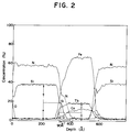
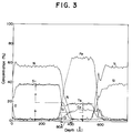
- Auger electron spectroscopy Using the sample disks prepared above, a depth-directional film structure analysis by Auger electron spectroscopy was carried out. There are shown Auger profiles of the sample disks in Figs. 1 to 3. Fig. 1 corresponds to Example; Fig. 2 corresponds to Comparison 1; and Fig. 3 corresponds to Comparison 2.
- the conditions of the Auger electron spectroscopy were as follows: Ion Energy: 1 kV Emission Current: 25 mA Measurement Area: 0.3 x 0.2 mm2 Sputter Rate: 81 ⁇ /min Acceleration Voltage: 2 kV Beam Current: 5 x 10 ⁇ 7 A Measurement Pressure: 6.8 x 10 ⁇ 8 Pa Spot Radius: 30 ⁇ m
- Example 2 a peak of oxygen bonded to the Tb layer exists between the Si3N4 dielectric film and the TbFeCo magnetic film. This peak of oxygen corresponds to the blocking layer, and it is understood that the blocking layer having a film thickness of about 50 ⁇ is formed.
- a degree of nitrogen (N) into the RE-TM magnetic film is less in Example than in Comparison 1 and Comparison 2. More specifically, as shown in Figs. 1 to 3, the degree of penetration from the interface is 60 ⁇ in Example. To the contrary, it is about 90 ⁇ in Comparison 1. Yet in Comparison 2 providing the Tb layer, it is about 80 ⁇ .
Abstract
Description
- The present invention relates to a magneto-optical recording medium having a rare earth - transition metal alloy film as a recording layer, and more particularly to an improvement for lowering of a recording magnetic field.
- In recent years, a magneto-optical recording system has been noticed as an overwritable high-density recording system. The magneto-optical recording system is such that a magnetic domain is written on a magnetic thin film to record information by using a thermal energy such as a semiconductor laser beam and this information is read by utilizing a magneto-optical effect.
- A typical recording material to be used in the magneto-optical recording system is known as a rare earth - transition metal alloy film (which will be hereinafter referred to as an RE-TM film) formed by combining a rare earth element such as Gd, Tb or Dy and a transition metal such as Fe or Co. As the magneto-optical recording medium having the RE-TM film as a recording layer, there has been proposed a recording medium having a four-layer structure consisting of an Si₃N₄ dielectric film, TbFeCo magnetic film, Si₃N₄ dielectric film and A1 reflecting film, for example.
- In manufacturing such a magneto-optical recording medium having the four-layer structure as mentioned above, it is necessary to sequentially form the Si₃N₄ dielectric film, the TbFeCo magnetic film, the Si₃N₄ dielectric film and the A1 reflecting film in this order on a substrate by sputtering or the like. In general, the Si₃N₄ dielectric film is formed by RF reactive sputtering in which an inert gas such as Ar and a reactive gas such as N₂ as a sputtering gas are introduced into a film forming chamber.
- However, in the magneto-optical recording medium to be manufactured by the above-mentioned technique, there is a problem such that unless recording is carried out in an external magnetic field of 150 Oe or more, a satisfactory CN ratio cannot be obtained. This problem is a large obstacle in case of applying the magneto-optical recording medium to an overwritable magnetic field modulation system. Accordingly, the elimination of this problem is a large subject for realizing the magnetic field modulation system.
- It is accordingly an object of the present invention to provide a magneto-optical recording medium which can suppress mixing of impurities into the TbFeCo magnetic film as a recording layer and lower a recording magnetic field.
- To achieve the above object, the present inventors have long studied to conclude that the characteristics are largely influenced by a degree of penetration of a constituent element of a dielectric layer into the TbFeCo magnetic film.
- The present invention has been accomplished on the basis of the above knowledge, and according to the present invention, there is provided in a magneto-optical recording medium having a substrate, a recording layer having at least a rare earth - transition metal alloy film formed on said substrate, and a dielectric layer formed on said recording layer; the improvement characterized in that a depth of an area in said recording layer containing an element derived from said dielectric layer is set to 70 Å or less from an interface between said recording layer and said dielectric layer in a depth-directional film structure analysis by Auger electron spectroscopy.
- In the magneto-optical recording medium according to the present invention, the RE-TM magnetic film is used as a recording layer, and at least a dielectric layer is formed on the RE-TM magnetic film. Specifically, the present invention may be applied to a magneto-optical recording medium having a four-layer structure consisting of an Si₃N₄ dielectric film, TbFeCo magnetic film, Si₃N₄ dielectric film and A1 reflecting film.
- As the RE-TM magnetic film to be used in the present invention, all of known magnetic materials such as TbFeCo or GdFeCo for a recording film of a conventional magneto-optical recording medium may be used. A film thickness of the RE-TM magnetic film is set to about 100 - 1000 Å from the viewpoint of practical magneto-optical characteristics.
- The recording layer may be constituted of the RE-TM magnetic film only, or may be constituted of the RE-TM magnetic film and a rare earth element layer such as a Tb layer formed on the RE-TM magnetic film. The rare earth element layer has an influence upon recording and reproducing characteristics and enables recording and reproduction under a low magnetic field. However, if a film thickness of the rare earth element layer is too large, a noise tends to increase. Accordingly, it is preferable to set the film thickness to about 1 - 30 Å.
- The dielectric layer is provided for the purposes of improvement in corrosion resistance and enhancement of Kerr rotation angle and Faraday rotation angle due to multiple reflection. The dielectric layer is formed of oxides, nitrides or oxynitrides of Si or the like or zinc sulfide (ZnS), for example. A film thickness of the dielectric layer is set to about 100 - 2000 Å. In the case that the dielectric layer is laminated on the recording layer (RE-TM film) or two of the dielectric layers are formed on both surfaces of the RE-TM magnetic film, the present invention is effective.
- In the case that the dielectric film is laminated on the recording layer (RE-TM magnetic film), there occurs a phenomenon such that a constituent element of the dielectric film penetrates into the RE-TM magnetic film to some extent depending upon film forming conditions.
- However, such an RE-TM magnetic film containing a constituent element of the dielectric film is not desired in the point of characteristics, and a proportion of such a penetration area in the RE-TM magnetic film largely influences a magnitude of an external magnetic field required for recording.
- In this circumstance, according to the present invention, a depth of an area in the recording layer containing an element derived from the dielectric layer is set to 70 Å or less from an interface between the recording layer and the dielectric layer.
- The interface between the recording layer and the dielectric layer is decided by a depth-directional film structure analysis by Auger electron spectroscopy, and it is defined in the present invention as follows:
- First, in a depth-directional Auger profile, an average peak level of Si in case of Si₃N₄ dielectric film or Zn in case of ZnS dielectric film is obtained, and a position in the dielectric layer on the interface side with respect to the recording layer where a peal level of Si (or Zn) becomes 1/2 of this average peal level is obtained.
- On the other hand, an average peal level of a rare earth element (e.g., Tb) of the RE-TM magnetic film is obtained, and a position in the recording layer on the interface side with respect to the dielectric layer where a peal level of the rare earth element becomes 1/2 of this average peak level.
- Finally, a middle point between the above two positions is defined as the interface between the recording layer and the dielectric layer.
- As to the area in the recording layer containing an element derived from the dielectric layer, this area corresponds to an area containing N in case of Si₃N₄ dielectric film, and it is determined by observing a degree of penetration of N from the interface into the recording layer. Similarly, in case of ZnS dielectrlc film, the area corresponds to an area containing S, and it is determined by observing a degree of penetration of S from the interface into the recording layer.
- The setting of such a degree of penetration of the element derived from the dielectric layer into the RE-TM magnetic film to 70 Å or less may be realized by providing a blocking layer at the interface between the dielectric layer and the recording layer.
- This blocking layer is a layer having a composition containing 3 % or more of a disiimllar element (e.g., oxygen) not existing in the RE-TM magnetic film. For example, an Auger signal of oxygen to be observed between the dielectric layer and the recording layer and an Auger signal of Tb to be observed by an increase in yield due to oxidation correspond to the blocking layer.
- A film thickness of the blocking layer may be obtained from a half width of a signal having a peak at the interface between the dielectric layer and the recording layer in the depth-directional Auger profile. The blocking layer is sufficiently effective even in the condition where an atom of the dissimilar element is arranged. From this viewpoint, the film thickness of the blocking layer may be several Å or more. However, if the film thickness of the blocking layer is too large, the characteristics of the recording layer (RE-TM magnetic film) is resultantly damaged, and it is therefore preferable to set the film thickness to 100 Å or less in terms of the above-mentioned half width.
- The formation of the blocking layer at the interface between the dielectric layer and the recording layer may be realized by the following manner. That is, after forming the RE-TM magnetic film or forming a rare earth element layer on the RE-TM magnetic film, the RE-TM magnetic film (or the rare earth element layer) is allowed to stand for 30 minutes or more. Alternatively, the RE-TM magnetic film (or the rare earth element layer) is exposed to an atmosphere having a predetermined oxygen partial pressure or an atmosphere having a predetermined oxygen partial pressure and a predetermined moisture partial pressure for a short time. The oxygen partial pressure may be set to about 1 x 10⁻¹⁰ - 1 x 10⁻¹ Torr, and the steam partial pressure may be set to about 1 x 10⁻¹⁰ - 1 x 10⁻¹ Torr. By setting the exposure time or other conditions within the above range, the blocking layer is formed.
- In manufacturing the magneto-optical recording medium having the four-layer structure as mentioned above, for example, the Si₃N₄ dielectric film of the third layer is formed by sputtering after forming the TbFeCo magnetic film of the second layer. Accordingly, the TbFeCo magnetic film is allowed to stand however for a very short time in contact with a plasma of Ar or N₂ gas as a film forming atmosphere for the Si₃N₄ dielectric film. Furthermore, the TbFeCo magnetic film is exposed to Si particles sputtered.
- At this time, there occurs a phenomenon such that an active element (especially, N or N⁺) dissociated or ionized in the plasma penetrates into the TbFeCo magnetic film to cause a deterioration in characteristics.
- However, according to the present invention, a depth of an area in the recording layer containing an element derived from the dielectric layer is set to 70 Å or less from the interface between the recording layer and the dielectric layer by a preferred technique of providing the blocking layer at the interface between the recording layer and the dielectric layer. Accordingly, the deterioration in characteristics can be suppressed to enable lowering of a recording magnetic field.
- That is, a degree of penetration of the element derived from the dielectric layer into the recording layer is set to 70 Å or less from the interface between the recording layer and the dielectric layer, thereby suppressing the deterioration in characteristics and improving a sensitivity to an external magnetic field.
- Other objects and features of the invention will be more fully understood from the following detailed description and appended claims when taken with the accompanying drawings.
- Fig. 1 is a graph illustrating an Auger profile in Example according to the present invention having a blocking layer;
- Fig. 2 is a graph illustrating an Auger profile in Comparison 1; and
- Fig. 3 is a graph illustrating an Auger profile in Comparison 2.
- The present invention will be more clearly understood with reference to the following examples.
- In Example, a magneto-optical recording medium having a four-layer structure consisting of an Si₃N₄ dielectric film, TbFeCo magnetic film, Si₃N₄ dielectric film and A1 reflecting film was prepared. In this four-layer structure, however, a Tb layer as a rear earth element layer was formed on the surface of the TbFeCo magnetic film. Further, a glass 2p substrate was used as a substrate of the recording medium.
- First, RF reactive sputtering was carried out by using an Si target in an Ar atmosphere containing 20 % of N² gas under the gas pressure of 3 x 10⁻³ Torr to form the first Si₃N₄ dielectric film.
- Then, direct current simultaneous two-element sputtering was carried out by using a Tb target and a FeCo alloy target to form the TbFeCo magnetic film having a film thickness of 225 Å.
- Then, direct current sputtering was carried out by using a Tb target to form the Tb layer having a film thickness of 5 Å.
- After forming the Tb layer, it was exposed to an atmosphere having a moisture partial pressure of 1 x 10⁻⁶ Torr and an oxygen partial pressure of 2 x 10⁻⁴ Torr for one minute to form a blocking layer.
- Then, RF reactive sputtering was carried out again by using an Si target to form the second Si₃N₄ dielectric film. Subsequently, direct current sputtering was carried out by using an A1 target to form the A1 reflecting film.
- Finally, UV curing resin was applied to the A1 reflecting film to form a protective film covering the A1 reflecting film. Thus, a sample disk was prepared.
- Similarly to Example, a sample disk was prepared with the exception that the film thickness of the TbFeCo magnetic film was set to 230 Å and the second Si₃N₄ dielectric film was formed immediately after forming the TbFeCo magnetic film.
-
- Similarly to Example, a sample disk was prepared with the exception that the second Si₃N₄ dielectric film was formed immediately after forming the Tb layer.
- Using the sample disks prepared above, a depth-directional film structure analysis by Auger electron spectroscopy was carried out. There are shown Auger profiles of the sample disks in Figs. 1 to 3. Fig. 1 corresponds to Example; Fig. 2 corresponds to Comparison 1; and Fig. 3 corresponds to Comparison 2. The conditions of the Auger electron spectroscopy were as follows:
Ion Energy: 1 kV Emission Current: 25 mA Measurement Area: 0.3 x 0.2 mm² Sputter Rate: 81 Å/min Acceleration Voltage: 2 kV Beam Current: 5 x 10⁻⁷ A Measurement Pressure: 6.8 x 10⁻⁸ Pa Spot Radius: 30 µm - As apparent from comparison of these Auger profiles, it is observed in Example that a peak of oxygen bonded to the Tb layer exists between the Si₃N₄ dielectric film and the TbFeCo magnetic film. This peak of oxygen corresponds to the blocking layer, and it is understood that the blocking layer having a film thickness of about 50 Å is formed.
- It is also understood that a degree of nitrogen (N) into the RE-TM magnetic film is less in Example than in Comparison 1 and Comparison 2. More specifically, as shown in Figs. 1 to 3, the degree of penetration from the interface is 60 Å in Example. To the contrary, it is about 90 Å in Comparison 1. Yet in Comparison 2 providing the Tb layer, it is about 80 Å.
- Next, a recording and reproducing characteristic of these sample disks by a magnetic field modulation system was investigated. The recording and reproducing characteristic was measured under the conditions of 1.3 m/sec of medium linear velocity, 720 kHz of recording frequency, 4.5 mW of recording laser power and 0.6 mW of reproducing laser power. A spectral analysis for a whole frequency band of a reproduced waveform was carried out with a resolution band of 10 kHz to obtain a CN ratio in a recording external magnetic field of ± 70 Oe. The result is shown in Table 1. As apparent from Table 1, a magnetic field sensitivity in Example is improved.
Table 1 Magnetic Film Structure H₂O Partial Pressure (Torr) O₂ Partial Pressure (Torr) Retention Time (min.) CN Ratio (dB) Example TbFeCo 225Å + Tb 5Å 1 x 10⁻⁶ 2 x 10⁻⁴ 1 48.6 Comparison 1 TbFeCo 230Å - - - 42.6 Comparison 2 bFeCo 225Å + Tb 5Å - - - 42.8 - While the invention has been described with reference to specific embodiments, the description is illustrative and is not to be construed as limiting the scope of the invention. Various modifications and changes may occur to those skilled in the art without departing from the spirit and scope of the invention as defined by the appended claims.
Claims (9)
- In a magneto-optical recording medium having a substrate, a recording layer having at least a rare earth - transition metal alloy film formed on said substrate, and a dielectric layer formed on said recording layer; the improvement characterized in that a depth of an area in said recording layer containing an element derived from said dielectric layer is set to 70 Å or less from an interface between said recording layer and said dielectric layer in a depth-directional film structure analysis by Auger electron spectroscopy.
- The magneto-optical recording medium as defined in claim 1, wherein said interface is located at a middle point between a first position in said dielectric layer and a second position in said recording layer, said first position corresponding to a half of an average peak level of a constituent element of said dielectric layer, said second position corresponding to a half of an average peak level of a rare earth element of said rare earth - transition metal alloy film.
- The magneto-optical recording medium as defined in claim 1, wherein the setting of the depth of said area to 70 Å or less is realized by providing a blocking layer at said interface, said blocking layer having a composition containing 3 % or more of a dissimilar element not existing in said rare earth - transition metal alloy film.
- The magneto-optical recording medium as defined in claim 3, wherein said dissimilar element is oxygen.
- The magneto-optical recording medium as defined in claim 3, wherein said blocking layer is formed by allowing said rare earth - transition metal alloy film to stand for 30 minutes or more after forming said rare earth - transition metal alloy film.
- The magneto-optical recording medium as defined in claim 3, wherein said blocking layer is formed by exposing said rare earth - transition metal alloy film to an atmosphere having a predetermined oxygen partial pressure for a short time after forming said rare earth - transition metal alloy film.
- The magneto-optical recording medium as defined in claim 6, wherein said predetermined oxygen partial pressure is set abpit 1 x 10⁻¹⁰ - 1 x 10⁻¹
- The magneto-optical recording medium as defined in claim 3, wherein said blocking layer is formed by exposing said rare earth - transition metal alloy film to an atmosphere having a predetermined oxygen partial pressure and a predetermined moisture partial pressure for a short time after forming said rare earth - transition metal alloy film.
- The magneto-optical recording medium as defined in claim 8, wherein said predetermined oxygen partial pressure is set to about 1 x 10⁻¹⁰ - 1 x 10⁻¹ Torr, and said predetermined partial pressure is set to about 1 x 10⁷ - 1 x 10⁴ Torr.
Applications Claiming Priority (4)
| Application Number | Priority Date | Filing Date | Title |
|---|---|---|---|
| JP5801491 | 1991-02-28 | ||
| JP58014/91 | 1991-02-28 | ||
| JP03059567A JP3122151B2 (en) | 1991-02-28 | 1991-03-01 | Magneto-optical recording medium |
| JP59567/91 | 1991-03-01 |
Publications (3)
| Publication Number | Publication Date |
|---|---|
| EP0502425A2 true EP0502425A2 (en) | 1992-09-09 |
| EP0502425A3 EP0502425A3 (en) | 1993-08-11 |
| EP0502425B1 EP0502425B1 (en) | 1998-04-15 |
Family
ID=26399104
Family Applications (1)
| Application Number | Title | Priority Date | Filing Date |
|---|---|---|---|
| EP92103365A Expired - Lifetime EP0502425B1 (en) | 1991-02-28 | 1992-02-27 | Method of producing a magneto-optical recording medium |
Country Status (7)
| Country | Link |
|---|---|
| US (2) | US5585197A (en) |
| EP (1) | EP0502425B1 (en) |
| JP (1) | JP3122151B2 (en) |
| KR (1) | KR100214037B1 (en) |
| AT (1) | ATE165184T1 (en) |
| CA (1) | CA2061954C (en) |
| DE (1) | DE69225083T2 (en) |
Cited By (2)
| Publication number | Priority date | Publication date | Assignee | Title |
|---|---|---|---|---|
| US5577020A (en) * | 1993-10-08 | 1996-11-19 | Tdk Corporation | Magneto-optical disc with intermediate film layer between a recording film and a dielectric film |
| US5593789A (en) * | 1993-12-14 | 1997-01-14 | Tdk Corporation | Magneto-optical recording medium |
Families Citing this family (2)
| Publication number | Priority date | Publication date | Assignee | Title |
|---|---|---|---|---|
| JPH11120635A (en) * | 1997-10-14 | 1999-04-30 | Sony Corp | Optical disk and its production |
| JP2000231749A (en) * | 1999-02-09 | 2000-08-22 | Sony Corp | Magneto-optical recording medium and its production |
Citations (3)
| Publication number | Priority date | Publication date | Assignee | Title |
|---|---|---|---|---|
| US4741967A (en) * | 1983-06-08 | 1988-05-03 | Canon Kabushiki Kaisha | Magnetic recording medium |
| EP0279581A2 (en) * | 1987-02-18 | 1988-08-24 | AT&T Corp. | Magneto-optic memory |
| EP0307554A1 (en) * | 1983-05-17 | 1989-03-22 | Minnesota Mining And Manufacturing Company | Amorphous magneto optical recording medium |
Family Cites Families (3)
| Publication number | Priority date | Publication date | Assignee | Title |
|---|---|---|---|---|
| JPH0766528B2 (en) * | 1983-03-18 | 1995-07-19 | 富士写真フイルム株式会社 | Magnetic recording medium |
| US4666759A (en) * | 1984-06-30 | 1987-05-19 | Kabushiki Kaisha Toshiba | Data recording medium |
| DE3803000A1 (en) * | 1988-02-02 | 1989-08-10 | Basf Ag | SURFACE MULTI-LAYER MAGNETO-OPTICAL RECORDING MATERIAL |
-
1991
- 1991-03-01 JP JP03059567A patent/JP3122151B2/en not_active Expired - Lifetime
-
1992
- 1992-02-25 KR KR1019920002844A patent/KR100214037B1/en not_active IP Right Cessation
- 1992-02-27 AT AT92103365T patent/ATE165184T1/en active
- 1992-02-27 CA CA002061954A patent/CA2061954C/en not_active Expired - Fee Related
- 1992-02-27 DE DE69225083T patent/DE69225083T2/en not_active Expired - Lifetime
- 1992-02-27 EP EP92103365A patent/EP0502425B1/en not_active Expired - Lifetime
-
1994
- 1994-08-11 US US08/289,346 patent/US5585197A/en not_active Expired - Lifetime
-
1996
- 1996-11-15 US US08/749,643 patent/US5741541A/en not_active Expired - Lifetime
Patent Citations (3)
| Publication number | Priority date | Publication date | Assignee | Title |
|---|---|---|---|---|
| EP0307554A1 (en) * | 1983-05-17 | 1989-03-22 | Minnesota Mining And Manufacturing Company | Amorphous magneto optical recording medium |
| US4741967A (en) * | 1983-06-08 | 1988-05-03 | Canon Kabushiki Kaisha | Magnetic recording medium |
| EP0279581A2 (en) * | 1987-02-18 | 1988-08-24 | AT&T Corp. | Magneto-optic memory |
Non-Patent Citations (1)
| Title |
|---|
| JOURNAL OF APPLIED PHYSICS vol. 67, no. 9, 1 May 1990, pages 5322 - 5324 K. C. KIM ET AL. 'Influence on the magnetic properties by the interface reaction between a TbCo thin film and a Si-contained protective layer' * |
Cited By (2)
| Publication number | Priority date | Publication date | Assignee | Title |
|---|---|---|---|---|
| US5577020A (en) * | 1993-10-08 | 1996-11-19 | Tdk Corporation | Magneto-optical disc with intermediate film layer between a recording film and a dielectric film |
| US5593789A (en) * | 1993-12-14 | 1997-01-14 | Tdk Corporation | Magneto-optical recording medium |
Also Published As
| Publication number | Publication date |
|---|---|
| EP0502425B1 (en) | 1998-04-15 |
| CA2061954C (en) | 2000-11-28 |
| KR100214037B1 (en) | 1999-08-02 |
| JP3122151B2 (en) | 2001-01-09 |
| US5741541A (en) | 1998-04-21 |
| EP0502425A3 (en) | 1993-08-11 |
| DE69225083D1 (en) | 1998-05-20 |
| ATE165184T1 (en) | 1998-05-15 |
| US5585197A (en) | 1996-12-17 |
| KR920017047A (en) | 1992-09-26 |
| JPH056582A (en) | 1993-01-14 |
| CA2061954A1 (en) | 1992-08-29 |
| DE69225083T2 (en) | 1998-11-19 |
Similar Documents
| Publication | Publication Date | Title |
|---|---|---|
| US5772856A (en) | Magneto-optical recording medium and method of manufacturing the same | |
| EP0449183B1 (en) | Magneto-optical recording medium | |
| US5577020A (en) | Magneto-optical disc with intermediate film layer between a recording film and a dielectric film | |
| US5476713A (en) | Magneto-optical recording medium | |
| EP0502425A2 (en) | Magneto-optical recording medium | |
| US5863649A (en) | Magneto-optical recording medium | |
| JPH09231631A (en) | Magneto-optical recording medium | |
| US4710434A (en) | Optomagnetic recording medium | |
| CA2292025C (en) | Magneto-optical recording medium and method for producing same | |
| EP0492584A2 (en) | Magneto-optical recording medium | |
| GB2158281A (en) | Optical recording medium | |
| JP3248278B2 (en) | Magneto-optical recording medium | |
| EP0350010B1 (en) | Magneto-optical recording medium | |
| US5536589A (en) | Magneto-optical recording medium | |
| US4999260A (en) | Magneto-optical recording medium comprising a rare-earth-transition metal dispersed in a dielectric | |
| JPS62281139A (en) | Magneto-optical disk | |
| US4803129A (en) | Magnetic recording material | |
| US6319623B1 (en) | Magneto-optical recording medium | |
| JP2507592B2 (en) | Optical recording medium | |
| KR940008647B1 (en) | Optical-magnetic recording medium | |
| JP2754658B2 (en) | Magneto-optical recording medium | |
| JPS6267750A (en) | Photomagnetic disk | |
| JPH0548539B2 (en) | ||
| JPH04188450A (en) | Magnetooptic recording medium | |
| JPH0532816B2 (en) |
Legal Events
| Date | Code | Title | Description |
|---|---|---|---|
| PUAI | Public reference made under article 153(3) epc to a published international application that has entered the european phase |
Free format text: ORIGINAL CODE: 0009012 |
|
| AK | Designated contracting states |
Kind code of ref document: A2 Designated state(s): AT DE FR GB |
|
| PUAL | Search report despatched |
Free format text: ORIGINAL CODE: 0009013 |
|
| AK | Designated contracting states |
Kind code of ref document: A3 Designated state(s): AT DE FR GB |
|
| 17P | Request for examination filed |
Effective date: 19940112 |
|
| 17Q | First examination report despatched |
Effective date: 19951026 |
|
| GRAG | Despatch of communication of intention to grant |
Free format text: ORIGINAL CODE: EPIDOS AGRA |
|
| GRAG | Despatch of communication of intention to grant |
Free format text: ORIGINAL CODE: EPIDOS AGRA |
|
| GRAH | Despatch of communication of intention to grant a patent |
Free format text: ORIGINAL CODE: EPIDOS IGRA |
|
| GRAH | Despatch of communication of intention to grant a patent |
Free format text: ORIGINAL CODE: EPIDOS IGRA |
|
| GRAA | (expected) grant |
Free format text: ORIGINAL CODE: 0009210 |
|
| AK | Designated contracting states |
Kind code of ref document: B1 Designated state(s): AT DE FR GB |
|
| REF | Corresponds to: |
Ref document number: 165184 Country of ref document: AT Date of ref document: 19980515 Kind code of ref document: T |
|
| REF | Corresponds to: |
Ref document number: 69225083 Country of ref document: DE Date of ref document: 19980520 |
|
| ET | Fr: translation filed | ||
| PLBE | No opposition filed within time limit |
Free format text: ORIGINAL CODE: 0009261 |
|
| STAA | Information on the status of an ep patent application or granted ep patent |
Free format text: STATUS: NO OPPOSITION FILED WITHIN TIME LIMIT |
|
| 26N | No opposition filed | ||
| REG | Reference to a national code |
Ref country code: GB Ref legal event code: IF02 |
|
| PGFP | Annual fee paid to national office [announced via postgrant information from national office to epo] |
Ref country code: DE Payment date: 20110218 Year of fee payment: 20 Ref country code: FR Payment date: 20110302 Year of fee payment: 20 Ref country code: AT Payment date: 20110214 Year of fee payment: 20 |
|
| PGFP | Annual fee paid to national office [announced via postgrant information from national office to epo] |
Ref country code: GB Payment date: 20110217 Year of fee payment: 20 |
|
| REG | Reference to a national code |
Ref country code: DE Ref legal event code: R071 Ref document number: 69225083 Country of ref document: DE |
|
| REG | Reference to a national code |
Ref country code: DE Ref legal event code: R071 Ref document number: 69225083 Country of ref document: DE |
|
| REG | Reference to a national code |
Ref country code: GB Ref legal event code: PE20 Expiry date: 20120226 |
|
| PG25 | Lapsed in a contracting state [announced via postgrant information from national office to epo] |
Ref country code: DE Free format text: LAPSE BECAUSE OF EXPIRATION OF PROTECTION Effective date: 20120228 |
|
| PG25 | Lapsed in a contracting state [announced via postgrant information from national office to epo] |
Ref country code: GB Free format text: LAPSE BECAUSE OF EXPIRATION OF PROTECTION Effective date: 20120226 |
|
| REG | Reference to a national code |
Ref country code: AT Ref legal event code: MK07 Ref document number: 165184 Country of ref document: AT Kind code of ref document: T Effective date: 20120227 |