EP0508664B1 - DC to DC converter - Google Patents
DC to DC converter Download PDFInfo
- Publication number
- EP0508664B1 EP0508664B1 EP92302818A EP92302818A EP0508664B1 EP 0508664 B1 EP0508664 B1 EP 0508664B1 EP 92302818 A EP92302818 A EP 92302818A EP 92302818 A EP92302818 A EP 92302818A EP 0508664 B1 EP0508664 B1 EP 0508664B1
- Authority
- EP
- European Patent Office
- Prior art keywords
- inductor means
- switching
- circuit
- switching device
- capacitance
- Prior art date
- Legal status (The legal status is an assumption and is not a legal conclusion. Google has not performed a legal analysis and makes no representation as to the accuracy of the status listed.)
- Expired - Lifetime
Links
Images


Classifications
-
- H—ELECTRICITY
- H02—GENERATION; CONVERSION OR DISTRIBUTION OF ELECTRIC POWER
- H02M—APPARATUS FOR CONVERSION BETWEEN AC AND AC, BETWEEN AC AND DC, OR BETWEEN DC AND DC, AND FOR USE WITH MAINS OR SIMILAR POWER SUPPLY SYSTEMS; CONVERSION OF DC OR AC INPUT POWER INTO SURGE OUTPUT POWER; CONTROL OR REGULATION THEREOF
- H02M3/00—Conversion of dc power input into dc power output
- H02M3/22—Conversion of dc power input into dc power output with intermediate conversion into ac
- H02M3/24—Conversion of dc power input into dc power output with intermediate conversion into ac by static converters
- H02M3/28—Conversion of dc power input into dc power output with intermediate conversion into ac by static converters using discharge tubes with control electrode or semiconductor devices with control electrode to produce the intermediate ac
- H02M3/325—Conversion of dc power input into dc power output with intermediate conversion into ac by static converters using discharge tubes with control electrode or semiconductor devices with control electrode to produce the intermediate ac using devices of a triode or a transistor type requiring continuous application of a control signal
- H02M3/335—Conversion of dc power input into dc power output with intermediate conversion into ac by static converters using discharge tubes with control electrode or semiconductor devices with control electrode to produce the intermediate ac using devices of a triode or a transistor type requiring continuous application of a control signal using semiconductor devices only
- H02M3/33569—Conversion of dc power input into dc power output with intermediate conversion into ac by static converters using discharge tubes with control electrode or semiconductor devices with control electrode to produce the intermediate ac using devices of a triode or a transistor type requiring continuous application of a control signal using semiconductor devices only having several active switching elements
- H02M3/33571—Half-bridge at primary side of an isolation transformer
Definitions
- This invention applies to the field of DC to DC power conversion and in particular to converters required to provide high power density.
- Patent SU-A-892614 which uses a single cored transformer with a single winding in the primary transformer circuit. From this document the features of the preamble of claim 1 are known.
- the present invention provides a DC to DC converter comprising: an input voltage source, a capacitance, an output circuit, a switching circuit for connecting the output alternatively across the voltage source and the capacitance; the output circuit further comprising primary inductor means coupled in series with the switching circuit whereby to produce a bidirectional current flow through the inductor means on operation of the switching means, secondary inductor means providing electrical isolation from and inductively coupled to the primary inductor means, the secondary inductor means including series coupled inductors, and first and second rectifiers each having a first terminal coupled to one of the series connected inductors respectively and second terminal connected to a common point for producing full wave rectification of current flowing in the secondary inductor means characterised in that the primary inductor means includes first inductor means and separate second inductor means coupled in series to the switching circuit, and the secondary inductor means includes a third inductor means and a separate fourth inductor means coupled in series, the first and third, and the second and fourth inductor means forming respective separate inductive coupling
- Figures 1 to 7 are intended to illustrate the principles of operation of power converters so as to enable an example of the invention shown in Figure 8 to be fully understood.
- Figures 1 to 7 are intended to illustrate the principles of operation of power converters so as to enable an example of the invention shown in Figure 8 to be fully understood.
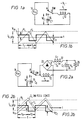
- a voltage source 14 supplies a voltage Vin to a flyback converter formed by a toggle switching device 12, a capacitor 16 of value C 1 , and an inductor 10 of value L.
- Switch 12 is assumed to be in position A for a time interval t 1 , then instantaneously moves to position B for a time interval t 2 .
- switch 12 connects inductor 10 alternatively across the input voltage source 14 and cross capacitor 16 .
- the important characteristic of this flyback converter is that due to the bidirectional nature of the switch 12, energy can flow from either voltage source 14 to capacitor 16 or vice versa during either position of the switch.
- a bridge rectifier 20 and a filter formed by inductor 22 with a value L f and capacitor 24 with a value C f are now connected across the inductor 10, with a resistor 26 loading the filter's output.
- Equation (7) shows the DC transfer characteristic of the circuit of Figure 2a, i.e., the value of its output voltage as a function of the input voltage and the operating duty cycle.
- Switch 12 in addition to driving the bidirectional flyback converter, also operates as a double ended converter in conjunction with the circuit connected in parallel to inductor 10, generating the output voltage given by equation (7).
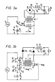
- One such circuit shown in Figure 3a can be obtained by using an isolation transformer 30 to connect the rectifier bridge 20, the filter 22-24, and the load 26 across the flyback inductor 10 .
- transformer 30 may be configured as an autotransformer and can have a center-tapped secondary or a multitude of secondaries if more than one output voltage is desired.
- Figure 3b can be compared to prior art circuits like the one disclosed in U.S. Patent 4,441,146.
- the toggle switch is realized using two MOS transistors 34 and 36, driven by two complementary signals so that when transistor 34 is on, transistor 36 is off and vice versa.
- a short delay time is provided between the turn-off of one transistor and the turn-on of the next. This delay will have no impact on the operation as described above, since when transistor 34 is turned off, the current of the flyback inductor (now the shunt inductance of transformer 30) will free wheel through the body diode of 36 and vice versa.
- the circuit shown in U.S. Patent 4,441,146 at Figure 4e is shown herein in Figure 3c, this being one of several possible embodiments.
- the components 38 and 40 form a "magnetizing current mirror" that resets the core of the transformer.
- the magnetizing inductance of the transformer 42 is fulfilling no useful purpose.
- the magnetizing inductance is kept at the highest value possible in order to minimize magnetizing current and, as opposed to the circuit of the present invention, eliminates any DC component from the core flux at any operating condition.
- Equation (8) assumes unity turns ratio for transformer 42.
- the significance of this result is that the filter inductor can be reduced by a factor of 4.33 in the circuit of Figure 3b for the same value of peak-to-peak ripple current in the output circuit as compared to a forward converter operating over the same range of input voltage and duty cycles.
- the capacitors across the devices are charged/discharged by the load current, thereby eliminating the turn on losses of the switches.
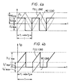
- I'o max is the value of the output current reflected to the primary of the transformer 30. This constraint will bring the magnetizing current of transformer 30 to change between zero and 2I'o max (ref. Fig. 4a) at full load and between -Io' max and +Io' max at no load.
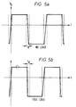
- the current in Q 1 , transistor 34 at the turn-off instant may vary from I'o max at no load to 3I'o max at full load, while the current in Q 2 , transistor 36 at turn off will be always equal to I'o max .
- These circuits will be available to charge/discharge capacitors 44 and 46 during the dead time intervals between the transistors conduction.
- Figure 4d shows the current of the primary winding 82 of transformer 30.
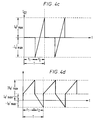
- ⁇ V max will occur at minimum input voltage and will be equal to 3.333 Vin min .
- Equation 15 allows us to choose arbitrarily either the value of the capacitors or the value of the dead time t d . For instance, when operating at a high frequency it may be desirable to use the drain-to-source capacitance of the transistors themselves to obtain zero voltage switching.
- Equation 15 By substituting the value of the capacitances in Equation 15 we can find the value of t d necessary to guarantee zero voltage switching. On some occasions the value of self-capacitance or parasitic capacitance of transistors 34 and 36 may be such that capacitors 44 and 46 are not necessary. The converter may still operate with zero switching losses using the self capacitance of transistors 34 and 36. Also, by making the peak-to-peak magnetizing current of the transformer either higher or lower than twice the reflected load current (Equation 13), we either increase the conduction losses in the switches and the primary of the transformer, or lose the zero voltage switching before reaching full load. Nevertheless, economic and other trade offs may dictate a relaxation of these constraints so only part of the potential improvement is realized.
- the output circuit includes two separate inductors 70 and 72 each having a value L/2 which is half the value of inductor 10 of Figure 1a.
- Inductors 70 and 72 are connected in series with diodes 74 and 76.
- a capacitor 78 is connected between the common terminal of the inductors and the common terminal of the diodes.
- the output circuit provides full wave rectification by using two rectifiers 74 and 76 and a capacitor 78.
- the output voltage across the load in Figure 7 is only one half the value of the voltage V 0 obtained by the output circuit of Figure 2a.
- An advantage of the output circuit of Figure 7 is the use of only two rectifiers instead of a full bridge rectifier.
- Another advantage is the use of the inductors 70 and 72 as both flyback converter inductor and output filter inductors for the output voltage.
- the output circuit is similar to the circuit disclosed in US patent No. 4,899, 271 issued to Seiersen.
- FIG 8 illustrates one embodiment of the invention.
- the output circuit includes two separate inductors 82 and 84 each having a value L/2 which is one half the value of inductor 10 of Figure 1a.
- Inductors 82 and 84 each have isolation windings 82a and 84a.
- Inductors 82 and 84 each have low magnetizing inductance.
- the isolation windings 82a and 84a are connected in series with diodes 80 and 86 connected at each end of the isolation windings.
- a capacitor 88 is connected between the common terminal of the isolation windings and the common terminal of the diodes.
- Load 90 is connected in parallel with capacitor 88.
- the output circuit provides full wave rectification by using two rectifiers 80 and 86 and a capacitor 88.
- the output circuit provides the benefits of isolation and voltage conversion, without the requirement of center tapping as is done in output circuits shown in Figure 3b and Figure 6. It should be appreciated that the topology of output circuit illustrated in Figure 8 can be independently utilised in many applications with full-wave rectification and isolation.
Description
Claims (8)
- A DC to DC converter comprising:an input voltage source (14);a capacitance (16) ;an output circuit;a switching circuit (12) for connecting the output alternatively across the voltage source and the capacitance;the output circuit further comprising primary inductor means (L1, L2; 82, 84) coupled in series with the switching circuit whereby to produce a bidirectional current flow through the inductor means on operation of the switching means, secondary inductor means providing electrical isolation from and inductively coupled to the primary inductor means, the secondary inductor means including series coupled inductors (82a, 84a), and first and second rectifiers (80,86) each having a first terminal coupled to one of the series connected inductors respectively and second terminal connected to a common point for producing full wave rectification of current flowing in the secondary inductor means characterised in that the primary inductor means includes first inductor means (82) and separate second inductor means (84) coupled in series to the switching circuit, and the secondary inductor means includes a third inductor means (82a) and a separate fourth inductor means (84a) coupled in series, the first and third, and the second and fourth inductor means forming respective separate inductive couplings.
- A converter according to claim 1 wherein the first (82) and second (84) inductor means are of substantially equal value.
- A converter according to claim 1 or 2 wherein the third (82a) and fourth (84a) inductor means are of substantially equal value.
- A converter according to any preceding claim wherein the switching circuit includes two electronic switching devices (Q1,Q2), the first switching device when closed connecting the output circuit across the input voltage source (14) and the second switching device when closed connects the output circuit across the capacitance (16).
- A converter according to claim 4 wherein said switching circuit switches said two switching devices (Q1, Q2) such that (a) said first switching device (Q1) is turned on while said second switching device (Q2) is off; (b) said first switching device is turned off and both said switching devices are off for a short dead-time interval; (c) said second switching device is turned on and said first switching device is off; (d) said second switching device is turned off and both said switching devices are off again for a short dead-time interval; and (e) the process is repeated periodically.
- A converter according to claim 5 further comprising capacitance (CS1, CS2) in parallel with at least one of said switching devices, so that voltage across said switching device is virtually zero prior to turning on or off.
- A converter according to claim 6 wherein said capacitance in parallel with said switching devices comprise self-capacitance of said electronic switching devices.
- A converter according to any preceding claim wherein said inductor means have substantially low magnetizing inductance.
Applications Claiming Priority (4)
| Application Number | Priority Date | Filing Date | Title |
|---|---|---|---|
| US68332391A | 1991-04-10 | 1991-04-10 | |
| US07/817,929 US5291382A (en) | 1991-04-10 | 1992-01-06 | Pulse width modulated DC/DC converter with reduced ripple current coponent stress and zero voltage switching capability |
| US817929 | 1992-01-06 | ||
| US683323 | 1996-07-18 |
Publications (2)
| Publication Number | Publication Date |
|---|---|
| EP0508664A1 EP0508664A1 (en) | 1992-10-14 |
| EP0508664B1 true EP0508664B1 (en) | 1998-07-22 |
Family
ID=27103075
Family Applications (1)
| Application Number | Title | Priority Date | Filing Date |
|---|---|---|---|
| EP92302818A Expired - Lifetime EP0508664B1 (en) | 1991-04-10 | 1992-03-31 | DC to DC converter |
Country Status (5)
| Country | Link |
|---|---|
| US (1) | US5291382A (en) |
| EP (1) | EP0508664B1 (en) |
| JP (1) | JPH05276751A (en) |
| DE (1) | DE69226300T2 (en) |
| HK (1) | HK1014806A1 (en) |
Cited By (3)
| Publication number | Priority date | Publication date | Assignee | Title |
|---|---|---|---|---|
| US8023290B2 (en) | 1997-01-24 | 2011-09-20 | Synqor, Inc. | High efficiency power converter |
| US10199950B1 (en) | 2013-07-02 | 2019-02-05 | Vlt, Inc. | Power distribution architecture with series-connected bus converter |
| RU2769718C1 (en) * | 2021-06-15 | 2022-04-05 | Акционерное общество "Научно-производственная фирма "СИГМА" | Method of controlling output voltage of dc-to-dc converters |
Families Citing this family (128)
| Publication number | Priority date | Publication date | Assignee | Title |
|---|---|---|---|---|
| USRE36098E (en) * | 1982-02-04 | 1999-02-16 | Vlt Corporation | Optimal resetting of the transformer's core in single-ended forward converters |
| US5327333A (en) * | 1992-11-25 | 1994-07-05 | At&T Bell Laboratories | Push push DC-DC reduced/zero voltage switching converter with off-set tapped secondary winding |
| US5363289A (en) * | 1992-12-15 | 1994-11-08 | At&T Bell Laboratories | Control apparatus for limiting voltage on a core reset capacitor |
| US5490055A (en) * | 1993-03-03 | 1996-02-06 | At&T Corp. | Multiloop feedback control apparatus for DC/DC converters with frequency-shaping band pass current control |
| US5303138A (en) * | 1993-04-29 | 1994-04-12 | At&T Bell Laboratories | Low loss synchronous rectifier for application to clamped-mode power converters |
| US5867379A (en) * | 1995-01-12 | 1999-02-02 | University Of Colorado | Non-linear carrier controllers for high power factor rectification |
| EP1278295A3 (en) | 1995-01-17 | 2004-12-29 | VLT, Inc. | Control of stored magnetic energy in power converter transformers |
| US5712772A (en) * | 1995-02-03 | 1998-01-27 | Ericsson Raynet | Controller for high efficiency resonant switching converters |
| US5694304A (en) * | 1995-02-03 | 1997-12-02 | Ericsson Raynet Corporation | High efficiency resonant switching converters |
| US5590032A (en) | 1995-05-25 | 1996-12-31 | Lucent Technologies Inc. | Self-synchronized drive circuit for a synchronous rectifier in a clamped-mode power converter |
| US5781058A (en) * | 1995-08-30 | 1998-07-14 | Cherry Semiconductor Corporation | Totem pole driver with cross conduction protection and default low impedance state output |
| US5841313A (en) * | 1995-08-30 | 1998-11-24 | Cherry Semiconductor Corporation | Switch with programmable delay |
| US5636107A (en) * | 1995-11-15 | 1997-06-03 | International Power Devices, Inc. | DC-DC converters |
| US5875103A (en) * | 1995-12-22 | 1999-02-23 | Electronic Measurements, Inc. | Full range soft-switching DC-DC converter |
| US5754413A (en) * | 1996-02-23 | 1998-05-19 | Lucent Technologies Inc. | Reduced voltage stress asymmetrical DC-to-DC converter using first and second transformers having differing turns ratios |
| US5784266A (en) * | 1996-06-14 | 1998-07-21 | Virginia Power Technologies, Inc | Single magnetic low loss high frequency converter |
| FR2751484B1 (en) * | 1996-07-16 | 1998-09-04 | Asulab Sa | CONTINUOUS POWER SUPPLY CIRCUIT REGULATED BY A REVERSIBLE CONVERTER |
| US5781420A (en) * | 1996-07-18 | 1998-07-14 | International Power Devices, Inc. | Single ended forward DC-to-DC converter providing enhanced resetting for synchronous rectification |
| US5896058A (en) * | 1997-03-31 | 1999-04-20 | Cherry Semiconductor Corporation | High speed totem pole FET driver circuit with differential cross conduction prevention |
| US5838552A (en) * | 1997-04-01 | 1998-11-17 | Lucent Technologies Inc | Asymmetrical power converter and method of operation thereof |
| US6069799A (en) * | 1997-05-14 | 2000-05-30 | Lucent Technologies Inc. | Self-synchronized drive circuit for a synchronous rectifier in a clamped-mode power converter |
| US6011703A (en) * | 1997-07-30 | 2000-01-04 | Lucent Technologies Inc. | Self-synchronized gate drive for power converter employing self-driven synchronous rectifier and method of operation thereof |
| US5877926A (en) * | 1997-10-10 | 1999-03-02 | Moisin; Mihail S. | Common mode ground fault signal detection circuit |
| US6188553B1 (en) | 1997-10-10 | 2001-02-13 | Electro-Mag International | Ground fault protection circuit |
| US6020688A (en) | 1997-10-10 | 2000-02-01 | Electro-Mag International, Inc. | Converter/inverter full bridge ballast circuit |
| DE19753358C2 (en) | 1997-12-02 | 2000-05-11 | Daimler Chrysler Ag | Connecting rod for a reciprocating piston machine and process for its manufacture |
| US6069455A (en) | 1998-04-15 | 2000-05-30 | Electro-Mag International, Inc. | Ballast having a selectively resonant circuit |
| US6091288A (en) * | 1998-05-06 | 2000-07-18 | Electro-Mag International, Inc. | Inverter circuit with avalanche current prevention |
| US6081432A (en) * | 1998-05-26 | 2000-06-27 | Artesyn Technologies, Inc. | Active reset forward converter employing synchronous rectifiers |
| US6028399A (en) * | 1998-06-23 | 2000-02-22 | Electro-Mag International, Inc. | Ballast circuit with a capacitive and inductive feedback path |
| US6100645A (en) * | 1998-06-23 | 2000-08-08 | Electro-Mag International, Inc. | Ballast having a reactive feedback circuit |
| US5999419A (en) * | 1998-08-07 | 1999-12-07 | National Semiconductor Corporation | Non-isolated boost converter with current steering |
| US6008999A (en) * | 1998-08-07 | 1999-12-28 | National Semiconductor Corporation | Non-isolated buck converter with input current steering |
| US6107750A (en) * | 1998-09-03 | 2000-08-22 | Electro-Mag International, Inc. | Converter/inverter circuit having a single switching element |
| US6160358A (en) * | 1998-09-03 | 2000-12-12 | Electro-Mag International, Inc. | Ballast circuit with lamp current regulating circuit |
| US6181082B1 (en) | 1998-10-15 | 2001-01-30 | Electro-Mag International, Inc. | Ballast power control circuit |
| US6137233A (en) * | 1998-10-16 | 2000-10-24 | Electro-Mag International, Inc. | Ballast circuit with independent lamp control |
| US6169375B1 (en) | 1998-10-16 | 2001-01-02 | Electro-Mag International, Inc. | Lamp adaptable ballast circuit |
| US6222326B1 (en) | 1998-10-16 | 2001-04-24 | Electro-Mag International, Inc. | Ballast circuit with independent lamp control |
| US6181083B1 (en) | 1998-10-16 | 2001-01-30 | Electro-Mag, International, Inc. | Ballast circuit with controlled strike/restart |
| US6127786A (en) * | 1998-10-16 | 2000-10-03 | Electro-Mag International, Inc. | Ballast having a lamp end of life circuit |
| US6091616A (en) * | 1998-10-21 | 2000-07-18 | Lucent Technologies Inc. | Drive compensation circuit for synchronous rectifier and method of operating the same |
| US6002597A (en) * | 1999-02-08 | 1999-12-14 | Lucent Technologies Inc. | Synchronous rectifier having dynamically adjustable current rating and method of operation thereof |
| US6100648A (en) * | 1999-04-30 | 2000-08-08 | Electro-Mag International, Inc. | Ballast having a resonant feedback circuit for linear diode operation |
| US6147886A (en) * | 1999-05-15 | 2000-11-14 | Technical Witts, Inc. | Dual opposed interleaved coupled inductor soft switching converters |
| US6272023B1 (en) | 1999-05-15 | 2001-08-07 | Technical Witts, Inc | High efficiency coupled inductor soft switching power converters |
| US6804129B2 (en) | 1999-07-22 | 2004-10-12 | 02 Micro International Limited | High-efficiency adaptive DC/AC converter |
| US6259615B1 (en) | 1999-07-22 | 2001-07-10 | O2 Micro International Limited | High-efficiency adaptive DC/AC converter |
| US6058026A (en) * | 1999-07-26 | 2000-05-02 | Lucent Technologies, Inc. | Multiple output converter having a single transformer winding and independent output regulation |
| US6130828A (en) * | 1999-08-26 | 2000-10-10 | Lucent Technologies, Inc. | Multiple output converter having self-synchronized pulse width modulation regulation |
| US6104623A (en) * | 1999-10-21 | 2000-08-15 | Lucent Technologies, Inc. | Multiple output converter having secondary regulator using self-driven synchronous rectifiers |
| CN1185781C (en) | 1999-11-05 | 2005-01-19 | 大动力公司 | Forward converter circuit having reduced switching losses |
| US6400579B2 (en) * | 2000-03-24 | 2002-06-04 | Slobodan Cuk | Lossless switching DC to DC converter with DC transformer |
| US6243278B1 (en) | 2000-04-04 | 2001-06-05 | Tyco Electronics Logistics A.G. | Drive circuit for synchronous rectifier and method of operating the same |
| EP1300055B1 (en) | 2000-05-12 | 2006-08-30 | O2 Micro International Limited | Integrated circuit for lamp heating and dimming control |
| US6218891B1 (en) | 2000-07-28 | 2001-04-17 | Lucent Technologies Inc. | Integrated circuit including a driver for a metal-semiconductor field-effect transistor |
| US6396725B1 (en) | 2000-07-31 | 2002-05-28 | Mark E. Jacobs | System and method for improving control loop response of a power supply |
| US6462962B1 (en) | 2000-09-08 | 2002-10-08 | Slobodan Cuk | Lossless switching DC-to-DC converter |
| US6400580B1 (en) | 2000-10-10 | 2002-06-04 | Wayne C. Bowman | System and method for reducing a DC magnetic flux bias in a transformer and power converter employing the same |
| US6501234B2 (en) | 2001-01-09 | 2002-12-31 | 02 Micro International Limited | Sequential burst mode activation circuit |
| US6570344B2 (en) | 2001-05-07 | 2003-05-27 | O2Micro International Limited | Lamp grounding and leakage current detection system |
| US6741061B2 (en) * | 2001-05-24 | 2004-05-25 | Comair Rotron, Inc. | Efficient stator |
| US6744647B2 (en) | 2001-06-04 | 2004-06-01 | Lambda Electronics, Inc. | Parallel connected converters apparatus and methods using switching cycle with energy holding state |
| US6606259B2 (en) | 2001-08-23 | 2003-08-12 | Lambda Electonics, Inc. | Clamped-inductance power converter apparatus with transient current limiting capability and operating methods therefor |
| US6442052B1 (en) | 2001-08-30 | 2002-08-27 | International Business Machines Corporation | High efficiency power converter with fast transient response |
| US6839590B2 (en) | 2001-10-22 | 2005-01-04 | Medtronic Physio-Control Corp. | Average current mode controlled energy storage in a defibrillator |
| US6788151B2 (en) | 2002-02-06 | 2004-09-07 | Lucent Technologies Inc. | Variable output power supply |
| US7046523B2 (en) * | 2002-04-18 | 2006-05-16 | Coldwatt, Inc. | Core structure and interleaved DC—DC converter topology |
| US7280026B2 (en) | 2002-04-18 | 2007-10-09 | Coldwatt, Inc. | Extended E matrix integrated magnetics (MIM) core |
| US7847494B2 (en) * | 2002-04-19 | 2010-12-07 | Linak A/S | Drive unit, preferably an actuator, a control and a construction |
| US20050207180A1 (en) * | 2002-04-23 | 2005-09-22 | Frans Pansier | Llc half-bridge converter |
| US7515446B2 (en) * | 2002-04-24 | 2009-04-07 | O2Micro International Limited | High-efficiency adaptive DC/AC converter |
| US6856519B2 (en) | 2002-05-06 | 2005-02-15 | O2Micro International Limited | Inverter controller |
| US6873322B2 (en) * | 2002-06-07 | 2005-03-29 | 02Micro International Limited | Adaptive LCD power supply circuit |
| US6756769B2 (en) | 2002-06-20 | 2004-06-29 | O2Micro International Limited | Enabling circuit for avoiding negative voltage transients |
| US6949912B2 (en) | 2002-06-20 | 2005-09-27 | 02Micro International Limited | Enabling circuit for avoiding negative voltage transients |
| US6765810B2 (en) * | 2002-08-02 | 2004-07-20 | Artesyn Technologies, Inc. | Full-wave coupled inductor power converter having synchronous rectifiers and two input switches that are simultaneously off for a time period of each switching cycle |
| US6778415B2 (en) * | 2003-01-22 | 2004-08-17 | O2Micro, Inc. | Controller electrical power circuit supplying energy to a display device |
| US7057611B2 (en) * | 2003-03-25 | 2006-06-06 | 02Micro International Limited | Integrated power supply for an LCD panel |
| US6936975B2 (en) * | 2003-04-15 | 2005-08-30 | 02Micro International Limited | Power supply for an LCD panel |
| US6897698B1 (en) | 2003-05-30 | 2005-05-24 | O2Micro International Limited | Phase shifting and PWM driving circuits and methods |
| DE102004033994B4 (en) * | 2003-07-16 | 2017-07-27 | Denso Corporation | DC-DC converter |
| US7394209B2 (en) * | 2004-02-11 | 2008-07-01 | 02 Micro International Limited | Liquid crystal display system with lamp feedback |
| US7427910B2 (en) * | 2004-08-19 | 2008-09-23 | Coldwatt, Inc. | Winding structure for efficient switch-mode power converters |
| US7321283B2 (en) * | 2004-08-19 | 2008-01-22 | Coldwatt, Inc. | Vertical winding structures for planar magnetic switched-mode power converters |
| JP4124814B2 (en) * | 2004-12-06 | 2008-07-23 | 株式会社デンソー | Input / output isolated DC-DC converter |
| US7417875B2 (en) * | 2005-02-08 | 2008-08-26 | Coldwatt, Inc. | Power converter employing integrated magnetics with a current multiplier rectifier and method of operating the same |
| US7876191B2 (en) * | 2005-02-23 | 2011-01-25 | Flextronics International Usa, Inc. | Power converter employing a tapped inductor and integrated magnetics and method of operating the same |
| US7176662B2 (en) * | 2005-02-23 | 2007-02-13 | Coldwatt, Inc. | Power converter employing a tapped inductor and integrated magnetics and method of operating the same |
| US7385375B2 (en) * | 2005-02-23 | 2008-06-10 | Coldwatt, Inc. | Control circuit for a depletion mode switch and method of operating the same |
| US8595041B2 (en) * | 2006-02-07 | 2013-11-26 | Sap Ag | Task responsibility system |
| US8125205B2 (en) * | 2006-08-31 | 2012-02-28 | Flextronics International Usa, Inc. | Power converter employing regulators with a coupled inductor |
| US7746670B2 (en) * | 2006-10-04 | 2010-06-29 | Denso Corporation | Dual-transformer type of DC-to-DC converter |
| JP4546439B2 (en) * | 2006-10-31 | 2010-09-15 | 株式会社デンソー | Magnetic circuit of 2-transform DCDC converter |
| US7675758B2 (en) * | 2006-12-01 | 2010-03-09 | Flextronics International Usa, Inc. | Power converter with an adaptive controller and method of operating the same |
| US7675759B2 (en) | 2006-12-01 | 2010-03-09 | Flextronics International Usa, Inc. | Power system with power converters having an adaptive controller |
| US9197132B2 (en) | 2006-12-01 | 2015-11-24 | Flextronics International Usa, Inc. | Power converter with an adaptive controller and method of operating the same |
| US7889517B2 (en) * | 2006-12-01 | 2011-02-15 | Flextronics International Usa, Inc. | Power system with power converters having an adaptive controller |
| US7667986B2 (en) * | 2006-12-01 | 2010-02-23 | Flextronics International Usa, Inc. | Power system with power converters having an adaptive controller |
| US7468649B2 (en) * | 2007-03-14 | 2008-12-23 | Flextronics International Usa, Inc. | Isolated power converter |
| US20080316779A1 (en) * | 2007-06-19 | 2008-12-25 | Chandrasekaran Jayaraman | System and method for estimating input power for a power processing circuit |
| US8040704B2 (en) * | 2007-06-30 | 2011-10-18 | Cuks, Llc | Integrated magnetics switching converter with zero inductor and output ripple currents and lossless switching |
| US7987928B2 (en) * | 2007-10-09 | 2011-08-02 | Pdti Holdings, Llc | Injection system and method comprising an impactor motive device |
| JP2009247121A (en) * | 2008-03-31 | 2009-10-22 | Fuji Electric Device Technology Co Ltd | Power conversion apparatus |
| CN102342008B (en) | 2009-01-19 | 2016-08-03 | 伟创力国际美国公司 | Controller for power converter |
| US8520414B2 (en) * | 2009-01-19 | 2013-08-27 | Power Systems Technologies, Ltd. | Controller for a power converter |
| WO2010114914A1 (en) | 2009-03-31 | 2010-10-07 | Flextronics International Usa, Inc. | Magnetic device formed with u-shaped core pieces and power converter employing the same |
| US9077248B2 (en) | 2009-06-17 | 2015-07-07 | Power Systems Technologies Ltd | Start-up circuit for a power adapter |
| US8514593B2 (en) * | 2009-06-17 | 2013-08-20 | Power Systems Technologies, Ltd. | Power converter employing a variable switching frequency and a magnetic device with a non-uniform gap |
| US8643222B2 (en) | 2009-06-17 | 2014-02-04 | Power Systems Technologies Ltd | Power adapter employing a power reducer |
| US20120170328A1 (en) * | 2009-06-19 | 2012-07-05 | Robertson Transformer Co. | Multimodal LED Power Supply With Wide Compliance Voltage and Safety Controlled Output |
| JP5640464B2 (en) * | 2009-07-29 | 2014-12-17 | Tdk株式会社 | Switching power supply |
| US8638578B2 (en) | 2009-08-14 | 2014-01-28 | Power System Technologies, Ltd. | Power converter including a charge pump employable in a power adapter |
| US8976549B2 (en) * | 2009-12-03 | 2015-03-10 | Power Systems Technologies, Ltd. | Startup circuit including first and second Schmitt triggers and power converter employing the same |
| US8520420B2 (en) * | 2009-12-18 | 2013-08-27 | Power Systems Technologies, Ltd. | Controller for modifying dead time between switches in a power converter |
| US8787043B2 (en) * | 2010-01-22 | 2014-07-22 | Power Systems Technologies, Ltd. | Controller for a power converter and method of operating the same |
| US9246391B2 (en) | 2010-01-22 | 2016-01-26 | Power Systems Technologies Ltd. | Controller for providing a corrected signal to a sensed peak current through a circuit element of a power converter |
| US8767418B2 (en) | 2010-03-17 | 2014-07-01 | Power Systems Technologies Ltd. | Control system for a power converter and method of operating the same |
| DE112011101073T5 (en) * | 2010-03-26 | 2013-01-10 | Power Systems Technologies,Ltd. | Power supply with a hub for a universal serial bus |
| US8792257B2 (en) | 2011-03-25 | 2014-07-29 | Power Systems Technologies, Ltd. | Power converter with reduced power dissipation |
| US8792256B2 (en) | 2012-01-27 | 2014-07-29 | Power Systems Technologies Ltd. | Controller for a switch and method of operating the same |
| US9190898B2 (en) | 2012-07-06 | 2015-11-17 | Power Systems Technologies, Ltd | Controller for a power converter and method of operating the same |
| US9099232B2 (en) | 2012-07-16 | 2015-08-04 | Power Systems Technologies Ltd. | Magnetic device and power converter employing the same |
| US9214264B2 (en) | 2012-07-16 | 2015-12-15 | Power Systems Technologies, Ltd. | Magnetic device and power converter employing the same |
| US9379629B2 (en) | 2012-07-16 | 2016-06-28 | Power Systems Technologies, Ltd. | Magnetic device and power converter employing the same |
| US9106130B2 (en) | 2012-07-16 | 2015-08-11 | Power Systems Technologies, Inc. | Magnetic device and power converter employing the same |
| US9240712B2 (en) | 2012-12-13 | 2016-01-19 | Power Systems Technologies Ltd. | Controller including a common current-sense device for power switches of a power converter |
| US9300206B2 (en) | 2013-11-15 | 2016-03-29 | Power Systems Technologies Ltd. | Method for estimating power of a power converter |
Citations (1)
| Publication number | Priority date | Publication date | Assignee | Title |
|---|---|---|---|---|
| SU892614A1 (en) * | 1980-04-11 | 1981-12-23 | Московский Ордена Ленина Энергетический Институт | One-cycle dc voltage regulator |
Family Cites Families (8)
| Publication number | Priority date | Publication date | Assignee | Title |
|---|---|---|---|---|
| US4618919A (en) * | 1984-10-04 | 1986-10-21 | Sperry Corporation | Topology for miniature power supply with low voltage and low ripple requirements |
| US4823249A (en) * | 1987-04-27 | 1989-04-18 | American Telephone And Telegraph Company At&T Bell Laboratories | High-frequency resonant power converter |
| DK382687A (en) * | 1987-07-22 | 1989-04-14 | Scanpower | POWER SUPPLY CIRCUIT |
| US4809148A (en) * | 1987-10-21 | 1989-02-28 | British Columbia Telephone Company | Full-fluxed, single-ended DC converter |
| US4945467A (en) * | 1988-02-26 | 1990-07-31 | Black & Decker Inc. | Multiple-mode voltage converter |
| US4975821A (en) * | 1989-10-10 | 1990-12-04 | Lethellier Patrice R | High frequency switched mode resonant commutation power supply |
| JPH0748944B2 (en) * | 1989-10-14 | 1995-05-24 | 東光株式会社 | DC-DC converter |
| US4959764A (en) * | 1989-11-14 | 1990-09-25 | Computer Products, Inc. | DC/DC converter switching at zero voltage |
-
1992
- 1992-01-06 US US07/817,929 patent/US5291382A/en not_active Expired - Lifetime
- 1992-03-31 EP EP92302818A patent/EP0508664B1/en not_active Expired - Lifetime
- 1992-03-31 DE DE69226300T patent/DE69226300T2/en not_active Expired - Fee Related
- 1992-04-09 JP JP4118123A patent/JPH05276751A/en active Pending
-
1998
- 1998-12-28 HK HK98116121A patent/HK1014806A1/en not_active IP Right Cessation
Patent Citations (1)
| Publication number | Priority date | Publication date | Assignee | Title |
|---|---|---|---|---|
| SU892614A1 (en) * | 1980-04-11 | 1981-12-23 | Московский Ордена Ленина Энергетический Институт | One-cycle dc voltage regulator |
Cited By (8)
| Publication number | Priority date | Publication date | Assignee | Title |
|---|---|---|---|---|
| US8023290B2 (en) | 1997-01-24 | 2011-09-20 | Synqor, Inc. | High efficiency power converter |
| US8493751B2 (en) | 1997-01-24 | 2013-07-23 | Synqor, Inc. | High efficiency power converter |
| US9143042B2 (en) | 1997-01-24 | 2015-09-22 | Synqor, Inc. | High efficiency power converter |
| US10199950B1 (en) | 2013-07-02 | 2019-02-05 | Vlt, Inc. | Power distribution architecture with series-connected bus converter |
| US10594223B1 (en) | 2013-07-02 | 2020-03-17 | Vlt, Inc. | Power distribution architecture with series-connected bus converter |
| US11075583B1 (en) | 2013-07-02 | 2021-07-27 | Vicor Corporation | Power distribution architecture with series-connected bus converter |
| US11705820B2 (en) | 2013-07-02 | 2023-07-18 | Vicor Corporation | Power distribution architecture with series-connected bus converter |
| RU2769718C1 (en) * | 2021-06-15 | 2022-04-05 | Акционерное общество "Научно-производственная фирма "СИГМА" | Method of controlling output voltage of dc-to-dc converters |
Also Published As
| Publication number | Publication date |
|---|---|
| HK1014806A1 (en) | 1999-09-30 |
| JPH05276751A (en) | 1993-10-22 |
| US5291382A (en) | 1994-03-01 |
| DE69226300D1 (en) | 1998-08-27 |
| EP0508664A1 (en) | 1992-10-14 |
| DE69226300T2 (en) | 1999-04-15 |
Similar Documents
| Publication | Publication Date | Title |
|---|---|---|
| EP0508664B1 (en) | DC to DC converter | |
| US5132888A (en) | Interleaved bridge converter | |
| US4788634A (en) | Resonant forward converter | |
| US6452814B1 (en) | Zero voltage switching cells for power converters | |
| US6198260B1 (en) | Zero voltage switching active reset power converters | |
| US5434768A (en) | Fixed frequency converter switching at zero voltage | |
| US4845605A (en) | High-frequency DC-DC power converter with zero-voltage switching of single primary-side power device | |
| US5838558A (en) | Phase staggered full-bridge converter with soft-PWM switching | |
| CA1209207A (en) | Regulated dc to dc converter | |
| US5991171A (en) | DC-to-DC converters | |
| US5521807A (en) | DC-To-DC converter with secondary flyback core reset | |
| US5140510A (en) | Constant frequency power converter | |
| US6016258A (en) | Full bridge DC-DC converters | |
| JP2875879B2 (en) | DC / DC switching converter circuit | |
| EP1120896B1 (en) | Resonant power converter | |
| US5065300A (en) | Class E fixed frequency converter | |
| US6272023B1 (en) | High efficiency coupled inductor soft switching power converters | |
| US6097614A (en) | Asymmetrical pulse width modulated resonant DC-DC converter with compensating circuitry | |
| US6590791B1 (en) | High input voltage, high efficiency, fast transient voltage regulator module (VRM) | |
| JP3317950B2 (en) | Active clamp forward converter | |
| US5151852A (en) | Class E power amplifier | |
| US6185111B1 (en) | Switching power supply apparatus | |
| US5523936A (en) | Built-in input filter forward converter | |
| US6166927A (en) | Push-pull power converter circuit | |
| US5920473A (en) | Dc-to-Dc power converter with integrated magnetic power transformer |
Legal Events
| Date | Code | Title | Description |
|---|---|---|---|
| PUAI | Public reference made under article 153(3) epc to a published international application that has entered the european phase |
Free format text: ORIGINAL CODE: 0009012 |
|
| AK | Designated contracting states |
Kind code of ref document: A1 Designated state(s): CH DE ES FR GB IT LI NL SE |
|
| 17P | Request for examination filed |
Effective date: 19930401 |
|
| 17Q | First examination report despatched |
Effective date: 19941230 |
|
| GRAG | Despatch of communication of intention to grant |
Free format text: ORIGINAL CODE: EPIDOS AGRA |
|
| GRAG | Despatch of communication of intention to grant |
Free format text: ORIGINAL CODE: EPIDOS AGRA |
|
| GRAH | Despatch of communication of intention to grant a patent |
Free format text: ORIGINAL CODE: EPIDOS IGRA |
|
| GRAH | Despatch of communication of intention to grant a patent |
Free format text: ORIGINAL CODE: EPIDOS IGRA |
|
| GRAA | (expected) grant |
Free format text: ORIGINAL CODE: 0009210 |
|
| AK | Designated contracting states |
Kind code of ref document: B1 Designated state(s): CH DE ES FR GB IT LI NL SE |
|
| PG25 | Lapsed in a contracting state [announced via postgrant information from national office to epo] |
Ref country code: CH Free format text: LAPSE BECAUSE OF FAILURE TO SUBMIT A TRANSLATION OF THE DESCRIPTION OR TO PAY THE FEE WITHIN THE PRESCRIBED TIME-LIMIT Effective date: 19980722 Ref country code: ES Free format text: THE PATENT HAS BEEN ANNULLED BY A DECISION OF A NATIONAL AUTHORITY Effective date: 19980722 Ref country code: NL Free format text: LAPSE BECAUSE OF FAILURE TO SUBMIT A TRANSLATION OF THE DESCRIPTION OR TO PAY THE FEE WITHIN THE PRESCRIBED TIME-LIMIT Effective date: 19980722 Ref country code: LI Free format text: LAPSE BECAUSE OF FAILURE TO SUBMIT A TRANSLATION OF THE DESCRIPTION OR TO PAY THE FEE WITHIN THE PRESCRIBED TIME-LIMIT Effective date: 19980722 |
|
| REG | Reference to a national code |
Ref country code: CH Ref legal event code: EP |
|
| REF | Corresponds to: |
Ref document number: 69226300 Country of ref document: DE Date of ref document: 19980827 |
|
| PG25 | Lapsed in a contracting state [announced via postgrant information from national office to epo] |
Ref country code: SE Free format text: LAPSE BECAUSE OF FAILURE TO SUBMIT A TRANSLATION OF THE DESCRIPTION OR TO PAY THE FEE WITHIN THE PRESCRIBED TIME-LIMIT Effective date: 19981022 |
|
| ET | Fr: translation filed | ||
| NLV1 | Nl: lapsed or annulled due to failure to fulfill the requirements of art. 29p and 29m of the patents act | ||
| REG | Reference to a national code |
Ref country code: CH Ref legal event code: PL |
|
| PLBE | No opposition filed within time limit |
Free format text: ORIGINAL CODE: 0009261 |
|
| STAA | Information on the status of an ep patent application or granted ep patent |
Free format text: STATUS: NO OPPOSITION FILED WITHIN TIME LIMIT |
|
| 26N | No opposition filed | ||
| REG | Reference to a national code |
Ref country code: GB Ref legal event code: IF02 |
|
| PGFP | Annual fee paid to national office [announced via postgrant information from national office to epo] |
Ref country code: FR Payment date: 20040302 Year of fee payment: 13 |
|
| PG25 | Lapsed in a contracting state [announced via postgrant information from national office to epo] |
Ref country code: IT Free format text: LAPSE BECAUSE OF NON-PAYMENT OF DUE FEES;WARNING: LAPSES OF ITALIAN PATENTS WITH EFFECTIVE DATE BEFORE 2007 MAY HAVE OCCURRED AT ANY TIME BEFORE 2007. THE CORRECT EFFECTIVE DATE MAY BE DIFFERENT FROM THE ONE RECORDED. Effective date: 20050331 |
|
| PGFP | Annual fee paid to national office [announced via postgrant information from national office to epo] |
Ref country code: GB Payment date: 20050802 Year of fee payment: 14 |
|
| PGFP | Annual fee paid to national office [announced via postgrant information from national office to epo] |
Ref country code: DE Payment date: 20050831 Year of fee payment: 14 |
|
| PG25 | Lapsed in a contracting state [announced via postgrant information from national office to epo] |
Ref country code: FR Free format text: LAPSE BECAUSE OF NON-PAYMENT OF DUE FEES Effective date: 20051130 |
|
| REG | Reference to a national code |
Ref country code: FR Ref legal event code: ST Effective date: 20051130 |
|
| PG25 | Lapsed in a contracting state [announced via postgrant information from national office to epo] |
Ref country code: GB Free format text: LAPSE BECAUSE OF NON-PAYMENT OF DUE FEES Effective date: 20060331 |
|
| PG25 | Lapsed in a contracting state [announced via postgrant information from national office to epo] |
Ref country code: DE Free format text: LAPSE BECAUSE OF NON-PAYMENT OF DUE FEES Effective date: 20061003 |
|
| GBPC | Gb: european patent ceased through non-payment of renewal fee |
Effective date: 20060331 |