EP0515024A2 - Circuit bypass device - Google Patents
Circuit bypass device Download PDFInfo
- Publication number
- EP0515024A2 EP0515024A2 EP92302443A EP92302443A EP0515024A2 EP 0515024 A2 EP0515024 A2 EP 0515024A2 EP 92302443 A EP92302443 A EP 92302443A EP 92302443 A EP92302443 A EP 92302443A EP 0515024 A2 EP0515024 A2 EP 0515024A2
- Authority
- EP
- European Patent Office
- Prior art keywords
- shunt
- conductive
- contacts
- coupled
- switching means
- Prior art date
- Legal status (The legal status is an assumption and is not a legal conclusion. Google has not performed a legal analysis and makes no representation as to the accuracy of the status listed.)
- Granted
Links
Images


Classifications
-
- H—ELECTRICITY
- H02—GENERATION; CONVERSION OR DISTRIBUTION OF ELECTRIC POWER
- H02H—EMERGENCY PROTECTIVE CIRCUIT ARRANGEMENTS
- H02H3/00—Emergency protective circuit arrangements for automatic disconnection directly responsive to an undesired change from normal electric working condition with or without subsequent reconnection ; integrated protection
- H02H3/20—Emergency protective circuit arrangements for automatic disconnection directly responsive to an undesired change from normal electric working condition with or without subsequent reconnection ; integrated protection responsive to excess voltage
- H02H3/207—Emergency protective circuit arrangements for automatic disconnection directly responsive to an undesired change from normal electric working condition with or without subsequent reconnection ; integrated protection responsive to excess voltage also responsive to under-voltage
-
- H—ELECTRICITY
- H01—ELECTRIC ELEMENTS
- H01H—ELECTRIC SWITCHES; RELAYS; SELECTORS; EMERGENCY PROTECTIVE DEVICES
- H01H61/00—Electrothermal relays
- H01H61/01—Details
- H01H61/0107—Details making use of shape memory materials
-
- H—ELECTRICITY
- H02—GENERATION; CONVERSION OR DISTRIBUTION OF ELECTRIC POWER
- H02H—EMERGENCY PROTECTIVE CIRCUIT ARRANGEMENTS
- H02H7/00—Emergency protective circuit arrangements specially adapted for specific types of electric machines or apparatus or for sectionalised protection of cable or line systems, and effecting automatic switching in the event of an undesired change from normal working conditions
- H02H7/18—Emergency protective circuit arrangements specially adapted for specific types of electric machines or apparatus or for sectionalised protection of cable or line systems, and effecting automatic switching in the event of an undesired change from normal working conditions for batteries; for accumulators
Definitions
- This invention relates to electrical switches and particularly to those switches that provide conductive shunts across circuit terminals.
- electrical shunts provide a conductive path between terminals in a circuit.
- shunts provide such paths upon the occurrence of certain triggering events.
- Shunts are useful for instance in bypassing faulty battery cells that are connected serially in power systems. In such systems, overall system failure can result from a single-cell failure. Such failure occurs when a cell becomes non-conductive due to an open circuit.
- a shunt switch is connected in parallel to the terminals of the cell. This connection permits current to flow around the cell.
- highly reliable shunt mechanisms for bypassing faulty cells are desirable. This is because power supplies are critical for operating such systems and any repair of the supplies is virtually impossible.
- HTR heat-to-recover
- U.S. Patent No. 4,700,259 to Stokes discloses an electrical circuit breaking device. The device breaks a conductor tensively in response to applied current.
- Soviet Union Patent No. 672674 to Korobov discloses a fuse. The fuse causes an open circuit by changing shape when heated. Current is applied to heat the fuse.
- U.S Patent No. 4,473,859 to Stone et al. discloses a piezoelectric circuit breaker with a bender. The bender responds to voltage changes by deflecting. The deflection then creates an open circuit.
- U.S. Patent No. 4,490,975 to Yaeger et al. discloses a self-protecting and conditioning memory metal actuator.
- the actuator uses a shape-memory spring that contracts due to temperature change. Current flow causes the temperature to change.
- U.S. Patent No. 4,524,343 to Morgan et al. discloses a self-regulated spring which operates an actuator. The actuator functions in a circuit-breaking application.
- U.S. Patent No. 4,825,184 to Bloch et al. discloses a current-controlled inductor.
- the inductor coil is made of shape memory alloy.
- U.S. Patent No. 3,573,550 to Baker discloses an automatically-resetting transient protection device.
- the device employs diodes connected to a power supply.
- the diodes serve to clamp the supply voltage at a certain level.
- a circuit bypass device (30) having terminals (70, 80) is connected to contacts (70, 80) of a cell (20) to provide a conductive path (40) in response to voltage excursion therebetween.
- Device (30) comprises: switching means (40), coupled to contacts (70, 80), having a conductive shunt (41, 42) that is movable from a normally non-conductive position to a conductive position between terminals (70, 80); detecting means (50), coupled to switching means (40) and to contacts (70, 80), for sensing voltage excursion beyond a specified limit between contacts (70, 80); and actuating means (60) coupled to switching means (40), having a heat-to-recover shape memory metal alloy that is formed to contract in response to detecting means (50) sensing voltage excursion, for moving conductive shunt (41, 42) from the non-conductive position to the conductive position.
- FIG. 1 is a block diagram of a battery system 10.
- System 10 is shown with a cell 20 and a bypass device 30 coupled at terminals 70, 80.
- FIG. 2 is a schematic diagram of a detector 50. Detector 50 is included in bypass device 30 of FIG. 1.
- FIGS. 3 and 4 are diagrams of a bypass device 31.
- Bypass device 31 is shown with an HTR element 61, 61'.
- HTR element 61, 61' contracts translationally to move a linear shunt 41, 41' from an open condition to a close condition.
- FIG. 3 shows the open condition
- FIG. 4 shows the close condition.
- FIGS. 5 and 6 are diagrams of a bypass device 32.
- Device 32 in one diagram is shown rotatably offset by 90 degrees from device 32 as shown in the other diagram.
- Device 32 is configured with an HTR element 62.
- HTR element 62 contracts torsionally to move a rotational shunt 42 rotatably. This movement provides a conductive path between detents 176 and detents 186.
- Detents 176 are shown in FIG. 5, and detents 186 are shown in FIG. 6.
- FIG. 7 shows a flattened view of the outer surface of rotational shunt 42. Angular displacements of rotational shunt 42 about line A-A of FIG. 5 are also shown.
- FIG. 1 a block diagram shows a power supply or battery system 10.
- System 10 comprises a battery or a cell 20 and a circuit bypass device 30 which are coupled at electrical contacts or terminals 70, 80.
- Cell 20 is connected to system 10 with terminal 70 being designated negatively (-) and terminal 80 being designated positively (+).
- Cell 20 may be a single cell or a combination of multiple cells. Such multiple cells may be arranged serially or in parallel with each other.
- system 10 couples device 30 in parallel to cell 20. This coupling provides a conductive electrical switch or shunt 40 between terminals 70, 80. In the event of an open circuit failure in cell 20 a low-resistance bypass path is created between terminals 70, 80. Cell 20 may be manifested by any electrical circuit requiring uninterrupted conduction between two nodes in the circuit.
- shunt 40 When device 30 is coupled initially to cell 20, shunt 40 is set open. Only negligible leakage current flows through diodes 53 and 54 as discussed later. Upon detection of an open circuit failure in cell 20, shunt 40 is triggered to switch selectively into a close position. Detection of the open circuit is accomplished by a detector 50. Detector 50 is coupled between terminals 70, 80 to sense the failures therebetween.
- Detector 50 is shown in FIG. 2.
- Detector 50 provides a conductive path between detector nodes 51, 52 when a voltage, V D , applied between nodes 51, 52 exceeds specified limits.
- Detector 50 includes a plurality of diodes 53, 54. These diodes 53, 54 are arranged serially between nodes 51, 52.
- Node 51 is connected to terminal 70, and node 52 is connected to heat-to-recover element (HTR) 60.
- HTR 60 is connected to shunt 40, which is then connected to terminal 80.
- V D The specified limits for V D vary depending on the direction of current flow through detector 50. In the charge direction from node 51 to node 52, current flows through single diode 53 when V D exceeds a 0.5 volt limit. This specified limit represents about one threshold drop. In the discharge direction from node 52 to node 51, current flows through three diodes 54 when V D exceeds a 1.5 volt limit. This specified limit represents about three threshold drops. Negligible leakage current through diodes 53, 54 flows between nodes 51, 52 when V D does not exceed the specified limits.
- terminal 70 is designated positively (+) and terminal 80 is designated negatively (-).
- detector 50 is assembled with diodes 53, 54 connected in the reverse direction.
- cell 20 may be assembled having a different number of diodes 53, 54.
- the accumulated threshold drops of diodes 53, 54 in a given direction correspond with the amount of V D that is anticipated to be applied to detector 50 in a given system 10.
- 1N3164-type diodes suffice as diodes 53, 54.
- the current ratings of the 1N3164-type diodes 53, 54 are based primarily on peak transient current rather than on continuous steady-state current.
- HTR 60 is made of heat-to-recover shape memory metal alloy.
- HTR 60 functions as an actuator to move shunt 40 into a conducting position between terminals 70, 80 in response to a voltage excursion detected therebetween.
- HTR 60 contracts to bias shunt 40 into a close position. Joule heating occurs as a function of I2R, where I is the current in amperes flowing through HTR 60 and R is the resistance in ohms of HTR 60.
- HTR 60 is formed preferably into a spring shape. This shape permits translational and torsional contraction of the HTR 60 metal alloy. HTR 60 may also be formed into non-spring shapes that are linearly and rotationally stretchable. One type of non-spring shape is a so-called torque tube. A torque tube comprises an empty cylinder having diagonal slot openings disposed longitudinally along the cylinder surface. HTR 60 may also be assembled from a combination of multiple stretchable elements. Such multiple elements may be attached serially or in parallel to each other to improve the biasing of shunt 40. Non-stretchable shapes of HTR 60 exhibit lesser contraction in response to thermal increases.
- the metal alloy of HTR 60 is capable of "remembering" its initially fabricated or pre-formed shape. When heated above a transformation temperature, T M-A , the HTR 60 alloy transitions from a martensitic state to an austenitic state. When austenitic HTR 60 recovers its initial physical dimensions. While martensitic the HTR 60 alloy is characteristically soft and malleable. Thus an HTR 60 spring in the martensitic state stretches easily and does not apply significant translational or torsional force to bias shunt 40.
- HTR 60 If sufficient current is passed through HTR 60 it becomes heated to temperatures above T M-A . At these temperatures the HTR 60 alloy becomes austenitic. When austenitic the HTR 60 spring hardens and contracts to return to its unstretched, original dimensions. During this contraction considerable force is applied by HTR 60 to bias shunt 40 rapidly into a close switch position. Biasing is accomplished torsionally and translationally. Since current stops flowing through HTR 60 upon the closing of shunt 40, HTR 60 cools to a temperature below T M-A . As a result of HTR 60 cooling, the force applied to bias shunt 40 becomes insignificant once again.
- the HTR 60 alloy is composed primarily of nickel and titanium.
- One such alloy may be obtained from Raychem Corporation in a (45-52%) nickel, (35-40%) titanium, (10-15%) niobium composition.
- This composition includes about 1-2% of other constituents.
- T M-A is approximately 175° C.
- T M-A varies depending on the particular composition.
- the first path is through cell 20. This path is available when cell 20 is functioning properly and not subject to an open circuit failure. However if an open circuit failure occurs in cell 20 then current flows through a second path. This path is through detector 50, HTR 60, and shunt 40. The second path is available only while V D exceeds specified limits and shunt 40 is set open. Finally once shunt 40 is switched into a close position, a third path is enabled through shunt 40.
- Detector 50 may be triggered remotely. Remote triggering allows detector 50 to detect a false open circuit condition and permits cell 20 to be bypassed selectively even if cell 20 is non-faulty. This type of bypassing might be desirable to preempt an anticipated open circuit failure. Remote triggering is accomplished by applying a voltage to terminals 70, 80 or nodes 51, 52 in an amount which is sufficient to cause V D excursion outside the specified limits.
- device 30 may be reset to reopen shunt 40.
- This resetting is performed much like a conventional circuit breaker might be reset.
- HTR 60 is cooled to a temperature sufficiently below a second transformation temperature, T A-M .
- T A-M the HTR 60 alloy transitions back to the martensitic state from the austenitic state.
- shunt 40 is returned mechanically to its initial open position.
- T M-A T A-M varies with alloy composition. For the described Raychem alloy composition, T A-M is approximately -30° C. Cooling is achieved by applying a coolant such as freon or liquid nitrogen directly onto HTR 60.
- FIGS. 3 and 4 illustrate a bypass device 31 that is configured with a translationally-contracting HTR 61, 61'.
- HTR 61 represents HTR element 60 in a stretched condition
- HTR 61' represents HTR element 60 in a contracted condition.
- device 31 is shown with a linear shunt 41 which is in an open condition.
- device 31 is shown with linear shunt 41' which is in a close condition.
- Terminals 71, 81 of device 31 are coupled respectively to terminals 70, 80 of cell 20.
- Device 31 is assembled in a case 91.
- Case 91 provides thermal insulation that is adequate to prevent transient external heat sources from raising the temperature therein to T M-A .
- Device 31 is assembled with terminal 71 connected to detector 50 at node 51.
- Detector 50 is also connected at node 52 to HTR 61.
- Shunt 41 and HTR 61 are connected as well.
- HTR 61 is stretched translationally between detector 50 and shunt 41. Since HTR 61 is martensitic when assembled initially in device 31, HTR 61 exerts insignificant force on shunt 41.
- Shunt 41 is connected to terminal 81 through detents 86 which hold shunt 41 in place at indentation 47. Detents 86 apply inward force to maintain electrical contact to shunt 41 through resilient prongs 88 extended from terminal 81.
- HTR 61 When detector 50 senses an open circuit failure HTR 61 is caused by detector 50 to contract translationally. This contraction causes shunt 41' to be pulled into a close position as shown in FIG. 4. As shunt 41' is biased to move toward terminal 71, detents 86 are disengaged from indentation 47 and then re-engaged at indentation 48. Detents 76 are pushed toward terminal 81 to slide up ramp 45 on shunt 41'. When pushed beyond ramp 45, detents 76 become engaged at indentation 46. Detents 76 apply inward force to maintain electrical contact to shunt 41' through resilient prongs 89 extended from terminal 71.
- Shunt 41, 41' is constructed of conductive material such as copper to provide low-resistance conduction between terminals 71, 81.
- ramp 45 is surface-coated with an electrical insulator such as fiberglass, ceramic, or polyimide. This insulation prevents detents 76 from engaging shunt 41' conductively before detents 76 are well-seated in indentations 46. In particular this insulation prevents HTR 61' from cooling prematurely and uncontracting before shunt 41' is switched completely into a close position.
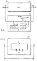
- FIGS. 5 and 6 an alternative bypass device 32 is illustrated.
- Device 32 is configured with a torsionally-contracting HTR 62 and a contactor barrel or rotational shunt 42.
- Shunt 42 is movable torsionally to provide electrical conductivity between terminals 72, 82.
- device 32 is potentially more compact since it does not require the additional longitudinal space that device 31 requires between terminals 71, 81. As described earlier such additional longitudinal space serves to permit translational movement of linear shunt 41.
- terminal 72 is shown connected to detents 176 through resilient prongs 189.
- Prongs 189 apply inward force to maintain electrical contact against the outer surface of shunt 42.
- device 32 is shown rotatably offset by 90 degrees from device 32 shown in FIG. 6.
- Terminal 82 is also shown connected to detents 186 through resilient prongs 188.
- prongs 188 apply inward force to maintain electrical contact against the outer surface of shunt 42.
- Terminals 72, 82 of device 32 are coupled respectively to terminals 70, 80 of cell 20.
- Device 32 is assembled in a case 92.
- Case 92 provides thermal insulation that is adequate to prevent transient external heat sources from raising the temperature therein to T M-A .
- Device 32 is assembled with terminal 72 connected to detector 50 at node 51.
- Detector 50 is also connected at node 52 to HTR 62.
- HTR 62 is connected to shunt 42.
- Shunt 42 is shown in FIG. 7 in a flattened view. The view indicates angular displacements about line A-A as shown in FIG. 5.
- Shunt 42 is cylindrical and includes on its outer surface insulating sections 145 and conductive strips 146, 147, 148. Strips 146, 147, 148 are manufactured with conductive material such as copper.
- Sections 145 are manufactured with insulating material such as fiberglass, polyimide, or ceramic.
- Shunt 42 is mounted rotatably on a non-conducting pivot pin 100 coupled to terminal 82.
- Strip 148 is wrapped continuously, i.e., 360 degrees, around the outer surface of shunt 42. Thus when shunt 42 rotates, detents 186 engage strip 148 continuously. Strips 147 connect strips 148, 146. Strips 146 are positioned discontinuously around the outer surface of shunt 42. Thus when shunt 42 rotates, electrical conductivity between terminals 72, 82 is provided when detents 176 conductively engage strips 146. However such conductivity is interrupted when detents 176 engage sections 145.
- HTR 62 When device 32 is coupled initially to cell 20, HTR 62 is twisted or deformed torsionally between detector 50 and shunt 42. Since HTR 62 is martensitic when assembled initially in device 32, HTR 62 exerts insignificant force on shunt 42. Also shunt 42 is set open initially by aligning detents 176 not to engage strips 146 conductively. Indentations may be placed on the outer surface of shunt 42 coinciding with strips 146 and sections 145. These indentations permit detents 176 to engage shunt 42 more securely.
- detector 50 When detector 50 senses an open circuit failure, detector 50 causes HTR 62 to contract torsionally. This contraction applies a torsional force to shunt 42. As a result of this torsional force, shunt 42 is displaced angularly about line A-A as shown in FIG. 5. Furthermore this displacement aligns detents 176 and strips 146 to contact each other. Such contact serves to provide conduction between terminals 72, 82.
- Additional strips 147, 146 may be interspersed on shunt 42. These additional strips 147, 146 provide more conduction points against which detents 176 may be aligned. Since additional strips 147, 146 reduce the angular displacement of shunt 42 that is necessary to provide conduction between strips 146 and detents 176, faster switching of device 32 is achieved.
Abstract
Description
- This is a subject invention under U.S. Government contract # NAS3-25082. As such the Government has rights therein.
- This invention relates to electrical switches and particularly to those switches that provide conductive shunts across circuit terminals.
- Unlike electrical fuses or circuit breakers electrical shunts provide a conductive path between terminals in a circuit. Typically shunts provide such paths upon the occurrence of certain triggering events. Shunts are useful for instance in bypassing faulty battery cells that are connected serially in power systems. In such systems, overall system failure can result from a single-cell failure. Such failure occurs when a cell becomes non-conductive due to an open circuit. To bypass the faulty cell a shunt switch is connected in parallel to the terminals of the cell. This connection permits current to flow around the cell. In space-borne systems, highly reliable shunt mechanisms for bypassing faulty cells are desirable. This is because power supplies are critical for operating such systems and any repair of the supplies is virtually impossible.
- Previously electromechanical switches were employed to bypass faulty cells. These switches were spring-loaded and triggered by fuses. In addition other types of switches were used for non-bypassing applications. These other switches employed various forms of triggering mechanisms. In particular certain other switches were triggered by so-called heat-to-recover (HTR) shape memory metal alloy elements. HTR elements change shape in response to thermal increase. Such thermal increase may be induced by current flow through the element.
- Switches that employ HTR elements however function as electrical fuses, not shunts. U.S. Patent No. 4,700,259 to Stokes discloses an electrical circuit breaking device. The device breaks a conductor tensively in response to applied current. Soviet Union Patent No. 672674 to Korobov discloses a fuse. The fuse causes an open circuit by changing shape when heated. Current is applied to heat the fuse. U.S Patent No. 4,473,859 to Stone et al. discloses a piezoelectric circuit breaker with a bender. The bender responds to voltage changes by deflecting. The deflection then creates an open circuit.
- U.S. Patent No. 4,490,975 to Yaeger et al. discloses a self-protecting and conditioning memory metal actuator. The actuator uses a shape-memory spring that contracts due to temperature change. Current flow causes the temperature to change. U.S. Patent No. 4,524,343 to Morgan et al. discloses a self-regulated spring which operates an actuator. The actuator functions in a circuit-breaking application. U.S. Patent No. 4,825,184 to Bloch et al. discloses a current-controlled inductor. The inductor coil is made of shape memory alloy.
- U.S. Patent No. 3,573,550 to Baker discloses an automatically-resetting transient protection device. The device employs diodes connected to a power supply. The diodes serve to clamp the supply voltage at a certain level.
- A circuit bypass device (30) having terminals (70, 80) is connected to contacts (70, 80) of a cell (20) to provide a conductive path (40) in response to voltage excursion therebetween. Device (30) comprises:
switching means (40), coupled to contacts (70, 80), having a conductive shunt (41, 42) that is movable from a normally non-conductive position to a conductive position between terminals (70, 80);
detecting means (50), coupled to switching means (40) and to contacts (70, 80), for sensing voltage excursion beyond a specified limit between contacts (70, 80); and
actuating means (60) coupled to switching means (40), having a heat-to-recover shape memory metal alloy that is formed to contract in response to detecting means (50) sensing voltage excursion, for moving conductive shunt (41, 42) from the non-conductive position to the conductive position. - FIG. 1 is a block diagram of a
battery system 10.System 10 is shown with acell 20 and abypass device 30 coupled atterminals 70, 80. - FIG. 2 is a schematic diagram of a
detector 50.Detector 50 is included inbypass device 30 of FIG. 1. - FIGS. 3 and 4 are diagrams of a bypass device 31. Bypass device 31 is shown with an
HTR element 61, 61'.HTR element 61, 61' contracts translationally to move alinear shunt 41, 41' from an open condition to a close condition. FIG. 3 shows the open condition, and FIG. 4 shows the close condition. - FIGS. 5 and 6 are diagrams of a
bypass device 32.Device 32 in one diagram is shown rotatably offset by 90 degrees fromdevice 32 as shown in the other diagram.Device 32 is configured with anHTR element 62.HTR element 62 contracts torsionally to move arotational shunt 42 rotatably. This movement provides a conductive path betweendetents 176 anddetents 186.Detents 176 are shown in FIG. 5, anddetents 186 are shown in FIG. 6. - FIG. 7 shows a flattened view of the outer surface of
rotational shunt 42. Angular displacements ofrotational shunt 42 about line A-A of FIG. 5 are also shown. - In FIG. 1 a block diagram shows a power supply or
battery system 10.System 10 comprises a battery or acell 20 and acircuit bypass device 30 which are coupled at electrical contacts orterminals 70, 80.Cell 20 is connected tosystem 10 with terminal 70 being designated negatively (-) and terminal 80 being designated positively (+).Cell 20 may be a single cell or a combination of multiple cells. Such multiple cells may be arranged serially or in parallel with each other. - Sometimes power supplies such as
cell 20 are subject to electrical discontinuities or open circuit failures. Accordinglysystem 10couples device 30 in parallel tocell 20. This coupling provides a conductive electrical switch or shunt 40 betweenterminals 70, 80. In the event of an open circuit failure in cell 20 a low-resistance bypass path is created betweenterminals 70, 80.Cell 20 may be manifested by any electrical circuit requiring uninterrupted conduction between two nodes in the circuit. - When
device 30 is coupled initially tocell 20,shunt 40 is set open. Only negligible leakage current flows throughdiodes cell 20,shunt 40 is triggered to switch selectively into a close position. Detection of the open circuit is accomplished by adetector 50.Detector 50 is coupled betweenterminals 70, 80 to sense the failures therebetween. -
Detector 50 is shown in FIG. 2.Detector 50 provides a conductive path betweendetector nodes nodes Detector 50 includes a plurality ofdiodes diodes nodes Node 51 is connected to terminal 70, andnode 52 is connected to heat-to-recover element (HTR) 60.HTR 60 is connected to shunt 40, which is then connected toterminal 80. - The specified limits for VD vary depending on the direction of current flow through
detector 50. In the charge direction fromnode 51 tonode 52, current flows throughsingle diode 53 when VD exceeds a 0.5 volt limit. This specified limit represents about one threshold drop. In the discharge direction fromnode 52 tonode 51, current flows through threediodes 54 when VD exceeds a 1.5 volt limit. This specified limit represents about three threshold drops. Negligible leakage current throughdiodes nodes - When the polarity of
cell 20 is reversed, terminal 70 is designated positively (+) andterminal 80 is designated negatively (-). With thesedesignations detector 50 is assembled withdiodes addition cell 20 may be assembled having a different number ofdiodes diodes detector 50 in a givensystem 10. Moreover for most shunting applications, 1N3164-type diodes suffice asdiodes type diodes - When
system 10 is operating, an open circuit failure may occur incell 20. If various external current sources or voltage sources are coupled tocell 20 throughterminals 70, 80 the current or voltage from these external sources is applied todevice 30 atterminals 70, 80. In particular the voltage that is applied externally atterminals 70, 80 is applied internally as well atnodes detector 50. This internal voltage application is due todetector 50,HTR 60, and shunt 40 being connected serially. If the voltage applied atnodes detector 50. - Current flowing through
detector 50 also flows throughHTR 60,shunt 40, andterminal 80.HTR 60 is made of heat-to-recover shape memory metal alloy. In accordance with an important aspect of the present invention,HTR 60 functions as an actuator to moveshunt 40 into a conducting position betweenterminals 70, 80 in response to a voltage excursion detected therebetween. - If heated sufficiently by the electrical power dissipation of the current flowing through
HTR 60,HTR 60 contracts to biasshunt 40 into a close position. Joule heating occurs as a function of I²R, where I is the current in amperes flowing throughHTR 60 and R is the resistance in ohms ofHTR 60. Onceshunt 40 is switched into a close position, a low-resistance, conductive path is formed betweenterminals 70, 80. Consequently voltage that is applied atnodes detector 50 andHTR 60 to stop flowing. -
HTR 60 is formed preferably into a spring shape. This shape permits translational and torsional contraction of theHTR 60 metal alloy.HTR 60 may also be formed into non-spring shapes that are linearly and rotationally stretchable. One type of non-spring shape is a so-called torque tube. A torque tube comprises an empty cylinder having diagonal slot openings disposed longitudinally along the cylinder surface.HTR 60 may also be assembled from a combination of multiple stretchable elements. Such multiple elements may be attached serially or in parallel to each other to improve the biasing ofshunt 40. Non-stretchable shapes ofHTR 60 exhibit lesser contraction in response to thermal increases. - The metal alloy of
HTR 60 is capable of "remembering" its initially fabricated or pre-formed shape. When heated above a transformation temperature, TM-A, theHTR 60 alloy transitions from a martensitic state to an austenitic state. Whenaustenitic HTR 60 recovers its initial physical dimensions. While martensitic theHTR 60 alloy is characteristically soft and malleable. Thus anHTR 60 spring in the martensitic state stretches easily and does not apply significant translational or torsional force to biasshunt 40. - If sufficient current is passed through
HTR 60 it becomes heated to temperatures above TM-A. At these temperatures theHTR 60 alloy becomes austenitic. When austenitic theHTR 60 spring hardens and contracts to return to its unstretched, original dimensions. During this contraction considerable force is applied byHTR 60 to biasshunt 40 rapidly into a close switch position. Biasing is accomplished torsionally and translationally. Since current stops flowing throughHTR 60 upon the closing ofshunt 40,HTR 60 cools to a temperature below TM-A. As a result ofHTR 60 cooling, the force applied to biasshunt 40 becomes insignificant once again. - The
HTR 60 alloy is composed primarily of nickel and titanium. One such alloy may be obtained from Raychem Corporation in a (45-52%) nickel, (35-40%) titanium, (10-15%) niobium composition. This composition includes about 1-2% of other constituents. Moreover for this composition, TM-A is approximately 175° C. However TM-A varies depending on the particular composition. - In summary three conductive paths are possible between
terminals 70, 80. The first path is throughcell 20. This path is available whencell 20 is functioning properly and not subject to an open circuit failure. However if an open circuit failure occurs incell 20 then current flows through a second path. This path is throughdetector 50,HTR 60, andshunt 40. The second path is available only while VD exceeds specified limits and shunt 40 is set open. Finally onceshunt 40 is switched into a close position, a third path is enabled throughshunt 40. -
Detector 50 may be triggered remotely. Remote triggering allowsdetector 50 to detect a false open circuit condition and permitscell 20 to be bypassed selectively even ifcell 20 is non-faulty. This type of bypassing might be desirable to preempt an anticipated open circuit failure. Remote triggering is accomplished by applying a voltage toterminals 70, 80 ornodes - After
device 30 is triggered to switchshunt 40 into a close position,device 30 may be reset to reopenshunt 40. This resetting is performed much like a conventional circuit breaker might be reset. To resetdevice 30,HTR 60 is cooled to a temperature sufficiently below a second transformation temperature, TA-M. At TA-M theHTR 60 alloy transitions back to the martensitic state from the austenitic state. WhenHTR 60 is martensitic,shunt 40 is returned mechanically to its initial open position. Like TM-A, TA-M varies with alloy composition. For the described Raychem alloy composition, TA-M is approximately -30° C. Cooling is achieved by applying a coolant such as freon or liquid nitrogen directly ontoHTR 60. - FIGS. 3 and 4 illustrate a bypass device 31 that is configured with a translationally-
contracting HTR 61, 61'.HTR 61 representsHTR element 60 in a stretched condition, and HTR 61' representsHTR element 60 in a contracted condition. In FIG. 3 device 31 is shown with alinear shunt 41 which is in an open condition. In FIG. 4 device 31 is shown with linear shunt 41' which is in a close condition.Terminals 71, 81 of device 31 are coupled respectively toterminals 70, 80 ofcell 20. Device 31 is assembled in acase 91.Case 91 provides thermal insulation that is adequate to prevent transient external heat sources from raising the temperature therein to TM-A. - Device 31 is assembled with terminal 71 connected to
detector 50 atnode 51.Detector 50 is also connected atnode 52 toHTR 61.Shunt 41 andHTR 61 are connected as well.HTR 61 is stretched translationally betweendetector 50 andshunt 41. SinceHTR 61 is martensitic when assembled initially in device 31,HTR 61 exerts insignificant force onshunt 41.Shunt 41 is connected to terminal 81 throughdetents 86 which holdshunt 41 in place atindentation 47.Detents 86 apply inward force to maintain electrical contact to shunt 41 throughresilient prongs 88 extended fromterminal 81. - When
detector 50 senses an opencircuit failure HTR 61 is caused bydetector 50 to contract translationally. This contraction causes shunt 41' to be pulled into a close position as shown in FIG. 4. As shunt 41' is biased to move toward terminal 71,detents 86 are disengaged fromindentation 47 and then re-engaged atindentation 48.Detents 76 are pushed towardterminal 81 to slide upramp 45 on shunt 41'. When pushed beyondramp 45,detents 76 become engaged atindentation 46.Detents 76 apply inward force to maintain electrical contact to shunt 41' throughresilient prongs 89 extended from terminal 71. -
Shunt 41, 41' is constructed of conductive material such as copper to provide low-resistance conduction betweenterminals 71, 81. To ensure thatdetents 76 are well-seated inindentations 46,ramp 45 is surface-coated with an electrical insulator such as fiberglass, ceramic, or polyimide. This insulation preventsdetents 76 from engaging shunt 41' conductively beforedetents 76 are well-seated inindentations 46. In particular this insulation prevents HTR 61' from cooling prematurely and uncontracting before shunt 41' is switched completely into a close position. - In FIGS. 5 and 6 an
alternative bypass device 32 is illustrated.Device 32 is configured with a torsionally-contracting HTR 62 and a contactor barrel orrotational shunt 42.Shunt 42 is movable torsionally to provide electrical conductivity betweenterminals device 32 is potentially more compact since it does not require the additional longitudinal space that device 31 requires betweenterminals 71, 81. As described earlier such additional longitudinal space serves to permit translational movement oflinear shunt 41. - In FIG. 5
terminal 72 is shown connected todetents 176 throughresilient prongs 189.Prongs 189 apply inward force to maintain electrical contact against the outer surface ofshunt 42. In FIG. 5device 32 is shown rotatably offset by 90 degrees fromdevice 32 shown in FIG. 6.Terminal 82 is also shown connected todetents 186 throughresilient prongs 188. Similarly toprongs 189,prongs 188 apply inward force to maintain electrical contact against the outer surface ofshunt 42.Terminals device 32 are coupled respectively toterminals 70, 80 ofcell 20.Device 32 is assembled in acase 92.Case 92 provides thermal insulation that is adequate to prevent transient external heat sources from raising the temperature therein to TM-A. -
Device 32 is assembled with terminal 72 connected todetector 50 atnode 51.Detector 50 is also connected atnode 52 toHTR 62. Inaddition HTR 62 is connected to shunt 42.Shunt 42 is shown in FIG. 7 in a flattened view. The view indicates angular displacements about line A-A as shown in FIG. 5.Shunt 42 is cylindrical and includes on its outersurface insulating sections 145 andconductive strips Strips Sections 145 are manufactured with insulating material such as fiberglass, polyimide, or ceramic.Shunt 42 is mounted rotatably on anon-conducting pivot pin 100 coupled toterminal 82. -
Strip 148 is wrapped continuously, i.e., 360 degrees, around the outer surface ofshunt 42. Thus whenshunt 42 rotates,detents 186 engagestrip 148 continuously.Strips 147 connectstrips Strips 146 are positioned discontinuously around the outer surface ofshunt 42. Thus whenshunt 42 rotates, electrical conductivity betweenterminals detents 176 conductively engage strips 146. However such conductivity is interrupted whendetents 176 engagesections 145. - When
device 32 is coupled initially tocell 20,HTR 62 is twisted or deformed torsionally betweendetector 50 andshunt 42. SinceHTR 62 is martensitic when assembled initially indevice 32,HTR 62 exerts insignificant force onshunt 42. Also shunt 42 is set open initially by aligningdetents 176 not to engagestrips 146 conductively. Indentations may be placed on the outer surface ofshunt 42 coinciding withstrips 146 andsections 145. These indentations permitdetents 176 to engageshunt 42 more securely. - When
detector 50 senses an open circuit failure,detector 50 causes HTR 62 to contract torsionally. This contraction applies a torsional force to shunt 42. As a result of this torsional force, shunt 42 is displaced angularly about line A-A as shown in FIG. 5. Furthermore this displacement alignsdetents 176 and strips 146 to contact each other. Such contact serves to provide conduction betweenterminals -
Additional strips shunt 42. Theseadditional strips additional strips shunt 42 that is necessary to provide conduction betweenstrips 146 anddetents 176, faster switching ofdevice 32 is achieved.
Claims (12)
- Apparatus having terminals for connection to a pair of contacts in a circuit to provide a conductive path in response to voltage excursion therebetween, the apparatus comprising:
switching means, coupled to the pair of contacts in the circuit, having a conductive shunt that is movable from a normally non-conductive position to a conductive position between the terminals;
detecting means, coupled to the switching means and to the pair of contacts, for sensing a voltage excursion beyond a specified limit between the contacts; and
actuating means, coupled to the switching means, having a heat-to-recover shape memory metal alloy that is formed to contract in response to the detecting means sensing the voltage excursion, for moving the conductive shunt from the non-conductive position to the conductive position. - The apparatus in claim 1, wherein:
the switching means includes a pair of detents, coupled to each terminal, for contacting the conductive shunt to provide conductivity through the detents between the terminals when the conductive shunt is moved to the conductive position. - The apparatus in claim 1, wherein:
the switching means includes a pair of resilient prongs, coupled to each terminal and to each detent, for applying inward force to each detent to maintain contact between the detent and the conductive shunt. - The apparatus in claim 1, wherein:
the switching means includes insulation on the conductive shunt to insulate the shunt from conduction between the terminals when the shunt is in the non-conductive position. - The apparatus in claim 1, wherein:
the detecting means comprises a plurality of diodes coupled serially between the contacts to sense the voltage excursion therebetween, the diodes permitting current flow between the contacts in response to sensing the voltage excursion beyond the specified limit. - The apparatus in claim 1, wherein:
the formed alloy contracts translationally to move the switching means linearly. - The apparatus in claim 1, wherein:
the formed alloy contracts torsionally to move the switching means rotatably. - The apparatus in claim 1, wherein:
the formed alloy is composed of titanium and nickel. - The apparatus in claim 1, wherein:
the formed alloy is a spring shape. - The apparatus in claim 1, wherein,
the formed alloy is initially in a martensitic state. - The apparatus in claim 1, wherein:
the switching means, the detecting means, and the actuating means are assembled in a thermally-insulating case. - An approved battery cell, comprising:
a cell having a pair of contacts; and
a device having terminals coupled to the pair of contacts in the cell to bypass the cell conductively in response to voltage excursion between the contacts;
wherein the device includes:
switching means, coupled to the contacts, having a conductive shunt that is movable between a conductive position and a non-conductive position between the terminal;
detecting means, coupled to the switching means and to the contacts, for sensing a voltage excursion beyond a specified limit between the contacts; and
actuating means, coupled to the switching means, having a heat-to-recover shape memory metal alloy that is formed to contract in response to the detecting means sensing the voltage excursions, for moving the conductive shunt from the non-conductive position to the conductive position.
Applications Claiming Priority (2)
| Application Number | Priority Date | Filing Date | Title |
|---|---|---|---|
| US07/704,772 US5206775A (en) | 1991-05-23 | 1991-05-23 | Circuit bypass device |
| US704772 | 1991-05-23 |
Publications (3)
| Publication Number | Publication Date |
|---|---|
| EP0515024A2 true EP0515024A2 (en) | 1992-11-25 |
| EP0515024A3 EP0515024A3 (en) | 1993-02-17 |
| EP0515024B1 EP0515024B1 (en) | 1995-09-06 |
Family
ID=24830808
Family Applications (1)
| Application Number | Title | Priority Date | Filing Date |
|---|---|---|---|
| EP92302443A Expired - Lifetime EP0515024B1 (en) | 1991-05-23 | 1992-03-20 | Circuit bypass device |
Country Status (5)
| Country | Link |
|---|---|
| US (1) | US5206775A (en) |
| EP (1) | EP0515024B1 (en) |
| JP (1) | JP2617400B2 (en) |
| CA (1) | CA2063977C (en) |
| DE (1) | DE69204542T2 (en) |
Cited By (3)
| Publication number | Priority date | Publication date | Assignee | Title |
|---|---|---|---|---|
| EP1111751A1 (en) * | 1999-12-23 | 2001-06-27 | Alcatel | Safety device for electric battery cells and battery provided with such a device |
| WO2001097720A3 (en) * | 2000-06-19 | 2002-08-15 | Simpler Networks | Bistable switch with shape memory metal |
| EP2747114A1 (en) * | 2012-12-21 | 2014-06-25 | Kidde Technologies, Inc. | Heat detector with shape metal alloy element |
Families Citing this family (13)
| Publication number | Priority date | Publication date | Assignee | Title |
|---|---|---|---|---|
| US5410290A (en) * | 1993-08-02 | 1995-04-25 | Cho; Dong-Il | Shape memory alloy relays and switches |
| JP3429932B2 (en) * | 1995-12-13 | 2003-07-28 | 三菱電機株式会社 | Power converter protection device |
| US5862995A (en) * | 1996-04-01 | 1999-01-26 | Diesel Technology Company | High pressure fluid passage sealing for internal combustion engine fuel injectors and method of making same |
| US5825850A (en) * | 1996-10-02 | 1998-10-20 | Time Warner Entertainment Co. L.P. | Automatic bypass switch for signal conductor |
| US7372355B2 (en) * | 2004-01-27 | 2008-05-13 | Black & Decker Inc. | Remote controlled wall switch actuator |
| ES2365917T3 (en) * | 2004-02-12 | 2011-10-13 | Mitsubishi Denki Kabushiki Kaisha | POWER CONVERTER. |
| US8153918B2 (en) * | 2005-01-27 | 2012-04-10 | Black & Decker Inc. | Automatic light switch with manual override |
| ATE456178T1 (en) * | 2006-06-07 | 2010-02-15 | Souriau | BRANCH DEVICE OF AN ELECTRICAL COMPONENT |
| US20080174182A1 (en) * | 2006-09-28 | 2008-07-24 | Siemens Energy And Automation, Inc. | Method for operating a multi-cell power supply having an integrated power cell bypass assembly |
| US8476864B2 (en) * | 2007-06-13 | 2013-07-02 | Lear Corporation | Battery monitoring system |
| US8830026B2 (en) * | 2010-12-30 | 2014-09-09 | General Electric Company | Shape memory alloy actuated circuit breaker |
| CN103247498A (en) * | 2013-03-29 | 2013-08-14 | 厦门赛尔特电子有限公司 | Temperature fuse with double pawl spring leaves |
| DE102016209757A1 (en) | 2016-06-03 | 2017-12-21 | Robert Bosch Gmbh | Device for increasing safety in dealing with a battery system |
Citations (10)
| Publication number | Priority date | Publication date | Assignee | Title |
|---|---|---|---|---|
| US3213345A (en) * | 1963-09-05 | 1965-10-19 | Mallory & Co Inc P R | Polarized shorting fuse for battery cells |
| US3573550A (en) * | 1969-03-07 | 1971-04-06 | M & T Chemicals Inc | Automatically resetting transient protection device |
| EP0026861A1 (en) * | 1979-10-03 | 1981-04-15 | Cerberus Ag | Arrangement for protection against overvoltage |
| US4490975A (en) * | 1983-03-14 | 1985-01-01 | Raychem Corporation | Self-protecting and conditioning memory metal actuator |
| US4524343A (en) * | 1984-01-13 | 1985-06-18 | Raychem Corporation | Self-regulated actuator |
| WO1985004045A1 (en) * | 1984-03-05 | 1985-09-12 | Hughes Aircraft Company | Thermally-activated, shorting diode switch having non-operationally-alternable junction path |
| EP0160533A2 (en) * | 1984-04-27 | 1985-11-06 | RAYCHEM CORPORATION (a Delaware corporation) | Shape memory effect actuator |
| US4825184A (en) * | 1987-07-06 | 1989-04-25 | The Boeing Company | Current controlled inductor |
| WO1990015430A1 (en) * | 1989-06-09 | 1990-12-13 | Raychem Corporation | Actuator |
| US5001446A (en) * | 1988-08-01 | 1991-03-19 | Matsushita Electric Works, Ltd. | Shape memory alloy and electric path protective device utilizing the alloy |
Family Cites Families (14)
| Publication number | Priority date | Publication date | Assignee | Title |
|---|---|---|---|---|
| US4028592A (en) * | 1972-12-22 | 1977-06-07 | Asea Aktiebolag | Means for increasing the stability in high-voltage power supply networks |
| US3957329A (en) * | 1974-11-01 | 1976-05-18 | I-T-E Imperial Corporation | Fault-current limiter for high power electrical transmission systems |
| SU672674A1 (en) * | 1978-01-03 | 1979-07-05 | Предприятие П/Я Г-4617 | Fuse |
| US4303877A (en) * | 1978-05-05 | 1981-12-01 | Brown, Boveri & Cie Aktiengesellschaft | Circuit for protecting storage cells |
| JPS5831657U (en) * | 1981-08-27 | 1983-03-01 | シャープ株式会社 | switch actuator |
| US4473859A (en) * | 1982-09-22 | 1984-09-25 | Piezo Electric Products, Inc. | Piezoelectric circuit breaker |
| US4559512A (en) * | 1983-03-14 | 1985-12-17 | Raychem Corporation | Self-protecting and conditioning memory metal actuator |
| JPS59152539U (en) * | 1983-03-30 | 1984-10-12 | 富士通株式会社 | temperature switch |
| AU585271B2 (en) * | 1984-11-16 | 1989-06-15 | University Of Sydney, The | An electrical circuit breaking device |
| JP2607367B2 (en) * | 1986-11-17 | 1997-05-07 | 時枝 直満 | Breaker |
| JPH01111440U (en) * | 1988-01-22 | 1989-07-27 | ||
| SE460323B (en) * | 1988-02-15 | 1989-09-25 | Asea Brown Boveri | Series capacitor EQUIPMENT |
| JPH0269441U (en) * | 1988-11-15 | 1990-05-25 | ||
| US4935315A (en) * | 1988-12-05 | 1990-06-19 | Hughes Aircraft Company | Cell bypass circuit |
-
1991
- 1991-05-23 US US07/704,772 patent/US5206775A/en not_active Expired - Fee Related
-
1992
- 1992-03-20 DE DE69204542T patent/DE69204542T2/en not_active Expired - Fee Related
- 1992-03-20 EP EP92302443A patent/EP0515024B1/en not_active Expired - Lifetime
- 1992-03-25 CA CA002063977A patent/CA2063977C/en not_active Expired - Fee Related
- 1992-05-25 JP JP4156238A patent/JP2617400B2/en not_active Expired - Fee Related
Patent Citations (10)
| Publication number | Priority date | Publication date | Assignee | Title |
|---|---|---|---|---|
| US3213345A (en) * | 1963-09-05 | 1965-10-19 | Mallory & Co Inc P R | Polarized shorting fuse for battery cells |
| US3573550A (en) * | 1969-03-07 | 1971-04-06 | M & T Chemicals Inc | Automatically resetting transient protection device |
| EP0026861A1 (en) * | 1979-10-03 | 1981-04-15 | Cerberus Ag | Arrangement for protection against overvoltage |
| US4490975A (en) * | 1983-03-14 | 1985-01-01 | Raychem Corporation | Self-protecting and conditioning memory metal actuator |
| US4524343A (en) * | 1984-01-13 | 1985-06-18 | Raychem Corporation | Self-regulated actuator |
| WO1985004045A1 (en) * | 1984-03-05 | 1985-09-12 | Hughes Aircraft Company | Thermally-activated, shorting diode switch having non-operationally-alternable junction path |
| EP0160533A2 (en) * | 1984-04-27 | 1985-11-06 | RAYCHEM CORPORATION (a Delaware corporation) | Shape memory effect actuator |
| US4825184A (en) * | 1987-07-06 | 1989-04-25 | The Boeing Company | Current controlled inductor |
| US5001446A (en) * | 1988-08-01 | 1991-03-19 | Matsushita Electric Works, Ltd. | Shape memory alloy and electric path protective device utilizing the alloy |
| WO1990015430A1 (en) * | 1989-06-09 | 1990-12-13 | Raychem Corporation | Actuator |
Cited By (7)
| Publication number | Priority date | Publication date | Assignee | Title |
|---|---|---|---|---|
| EP1111751A1 (en) * | 1999-12-23 | 2001-06-27 | Alcatel | Safety device for electric battery cells and battery provided with such a device |
| FR2803123A1 (en) * | 1999-12-23 | 2001-06-29 | Cit Alcatel | SAFETY DEVICE FOR ELECTRICAL BATTERY AND BATTERY EQUIPPED WITH SUCH DEVICE |
| US6741437B2 (en) | 1999-12-23 | 2004-05-25 | Alcatel | Safety device for electrical storage cell battery and battery equipped with the device |
| WO2001097720A3 (en) * | 2000-06-19 | 2002-08-15 | Simpler Networks | Bistable switch with shape memory metal |
| US6917276B1 (en) | 2000-06-19 | 2005-07-12 | Simpler Networks | Bistable switch with shape memory metal |
| EP2747114A1 (en) * | 2012-12-21 | 2014-06-25 | Kidde Technologies, Inc. | Heat detector with shape metal alloy element |
| US9524841B2 (en) | 2012-12-21 | 2016-12-20 | Kidde Technologies, Inc. | Heat detector with shape metal alloy element |
Also Published As
| Publication number | Publication date |
|---|---|
| DE69204542T2 (en) | 1996-05-15 |
| US5206775A (en) | 1993-04-27 |
| DE69204542D1 (en) | 1995-10-12 |
| CA2063977C (en) | 2000-08-29 |
| EP0515024B1 (en) | 1995-09-06 |
| JPH06189460A (en) | 1994-07-08 |
| EP0515024A3 (en) | 1993-02-17 |
| JP2617400B2 (en) | 1997-06-04 |
| CA2063977A1 (en) | 1992-11-24 |
Similar Documents
| Publication | Publication Date | Title |
|---|---|---|
| US5206775A (en) | Circuit bypass device | |
| US4652964A (en) | Varistor fuse element | |
| Strumpler et al. | Novel medium voltage fault current limiter based on polymer PTC resistors | |
| US4583146A (en) | Fault current interrupter | |
| US5438173A (en) | Cell bypass switch | |
| AU687284B2 (en) | Surge arrester with overvoltage sensitive grounding switch | |
| CN101241926A (en) | Programmable phase change material structure and its forming method | |
| DE102012004678A1 (en) | Surge protection device | |
| US6862164B2 (en) | Circuit protection arrangement | |
| US11218004B2 (en) | Arrangement having a multifunctional connection for energy storage cells or energy consumers | |
| EP0966748A1 (en) | Circuit breaker with improved arc interruption function | |
| US5898239A (en) | Automatic electronic bypass power switch | |
| WO2011054523A1 (en) | Electrical device | |
| US5362576A (en) | Current-activated bypass switch | |
| DE19744011A1 (en) | Circuit breaker device for power supply and distribution | |
| JPS60165775A (en) | Shorting switch unit of superconductive magnet coil | |
| EP1986212B1 (en) | Trip indicator member, and limiter and electrical switching apparatus including a plurality of trip indicator members | |
| US4520246A (en) | On-load tap changer of the type of vacuum switches | |
| WO2021001017A1 (en) | Switching device | |
| US11509159B2 (en) | System and method for thermal cutoff protection device control from an external component | |
| JPH04207923A (en) | Current limiting method and current limiter | |
| EP4235724A2 (en) | Thermal protection device to withstand high voltage | |
| JPH01185128A (en) | Self-reset current limiter | |
| GB2355340A (en) | Thermally activated switch mechanism | |
| EP0990294A1 (en) | A device for current limitation and protection against faults in a current |
Legal Events
| Date | Code | Title | Description |
|---|---|---|---|
| PUAI | Public reference made under article 153(3) epc to a published international application that has entered the european phase |
Free format text: ORIGINAL CODE: 0009012 |
|
| AK | Designated contracting states |
Kind code of ref document: A2 Designated state(s): DE FR GB IT |
|
| PUAL | Search report despatched |
Free format text: ORIGINAL CODE: 0009013 |
|
| AK | Designated contracting states |
Kind code of ref document: A3 Designated state(s): DE FR GB IT |
|
| 17P | Request for examination filed |
Effective date: 19930315 |
|
| 17Q | First examination report despatched |
Effective date: 19931025 |
|
| GRAA | (expected) grant |
Free format text: ORIGINAL CODE: 0009210 |
|
| AK | Designated contracting states |
Kind code of ref document: B1 Designated state(s): DE FR GB IT |
|
| ITF | It: translation for a ep patent filed |
Owner name: JACOBACCI & PERANI S.P.A. |
|
| REF | Corresponds to: |
Ref document number: 69204542 Country of ref document: DE Date of ref document: 19951012 |
|
| ET | Fr: translation filed | ||
| PLBE | No opposition filed within time limit |
Free format text: ORIGINAL CODE: 0009261 |
|
| STAA | Information on the status of an ep patent application or granted ep patent |
Free format text: STATUS: NO OPPOSITION FILED WITHIN TIME LIMIT |
|
| 26N | No opposition filed | ||
| REG | Reference to a national code |
Ref country code: GB Ref legal event code: IF02 |
|
| PGFP | Annual fee paid to national office [announced via postgrant information from national office to epo] |
Ref country code: FR Payment date: 20030304 Year of fee payment: 12 |
|
| PGFP | Annual fee paid to national office [announced via postgrant information from national office to epo] |
Ref country code: GB Payment date: 20030312 Year of fee payment: 12 |
|
| PGFP | Annual fee paid to national office [announced via postgrant information from national office to epo] |
Ref country code: DE Payment date: 20030331 Year of fee payment: 12 |
|
| PG25 | Lapsed in a contracting state [announced via postgrant information from national office to epo] |
Ref country code: GB Free format text: LAPSE BECAUSE OF NON-PAYMENT OF DUE FEES Effective date: 20040320 |
|
| PG25 | Lapsed in a contracting state [announced via postgrant information from national office to epo] |
Ref country code: DE Free format text: LAPSE BECAUSE OF NON-PAYMENT OF DUE FEES Effective date: 20041001 |
|
| GBPC | Gb: european patent ceased through non-payment of renewal fee |
Effective date: 20040320 |
|
| PG25 | Lapsed in a contracting state [announced via postgrant information from national office to epo] |
Ref country code: FR Free format text: LAPSE BECAUSE OF NON-PAYMENT OF DUE FEES Effective date: 20041130 |
|
| REG | Reference to a national code |
Ref country code: FR Ref legal event code: ST |
|
| PG25 | Lapsed in a contracting state [announced via postgrant information from national office to epo] |
Ref country code: IT Free format text: LAPSE BECAUSE OF NON-PAYMENT OF DUE FEES;WARNING: LAPSES OF ITALIAN PATENTS WITH EFFECTIVE DATE BEFORE 2007 MAY HAVE OCCURRED AT ANY TIME BEFORE 2007. THE CORRECT EFFECTIVE DATE MAY BE DIFFERENT FROM THE ONE RECORDED. Effective date: 20050320 |