EP0524653A2 - Bar code reader - Google Patents
Bar code reader Download PDFInfo
- Publication number
- EP0524653A2 EP0524653A2 EP92112740A EP92112740A EP0524653A2 EP 0524653 A2 EP0524653 A2 EP 0524653A2 EP 92112740 A EP92112740 A EP 92112740A EP 92112740 A EP92112740 A EP 92112740A EP 0524653 A2 EP0524653 A2 EP 0524653A2
- Authority
- EP
- European Patent Office
- Prior art keywords
- bar code
- code reader
- amplifier
- signal
- circuit
- Prior art date
- Legal status (The legal status is an assumption and is not a legal conclusion. Google has not performed a legal analysis and makes no representation as to the accuracy of the status listed.)
- Granted
Links
Images


Classifications
-
- G—PHYSICS
- G06—COMPUTING; CALCULATING OR COUNTING
- G06K—GRAPHICAL DATA READING; PRESENTATION OF DATA; RECORD CARRIERS; HANDLING RECORD CARRIERS
- G06K7/00—Methods or arrangements for sensing record carriers, e.g. for reading patterns
- G06K7/10—Methods or arrangements for sensing record carriers, e.g. for reading patterns by electromagnetic radiation, e.g. optical sensing; by corpuscular radiation
- G06K7/10544—Methods or arrangements for sensing record carriers, e.g. for reading patterns by electromagnetic radiation, e.g. optical sensing; by corpuscular radiation by scanning of the records by radiation in the optical part of the electromagnetic spectrum
- G06K7/10821—Methods or arrangements for sensing record carriers, e.g. for reading patterns by electromagnetic radiation, e.g. optical sensing; by corpuscular radiation by scanning of the records by radiation in the optical part of the electromagnetic spectrum further details of bar or optical code scanning devices
- G06K7/10841—Particularities of the light-sensitive elements
-
- G—PHYSICS
- G06—COMPUTING; CALCULATING OR COUNTING
- G06K—GRAPHICAL DATA READING; PRESENTATION OF DATA; RECORD CARRIERS; HANDLING RECORD CARRIERS
- G06K7/00—Methods or arrangements for sensing record carriers, e.g. for reading patterns
- G06K7/10—Methods or arrangements for sensing record carriers, e.g. for reading patterns by electromagnetic radiation, e.g. optical sensing; by corpuscular radiation
- G06K7/10544—Methods or arrangements for sensing record carriers, e.g. for reading patterns by electromagnetic radiation, e.g. optical sensing; by corpuscular radiation by scanning of the records by radiation in the optical part of the electromagnetic spectrum
- G06K7/10821—Methods or arrangements for sensing record carriers, e.g. for reading patterns by electromagnetic radiation, e.g. optical sensing; by corpuscular radiation by scanning of the records by radiation in the optical part of the electromagnetic spectrum further details of bar or optical code scanning devices
- G06K7/10851—Circuits for pulse shaping, amplifying, eliminating noise signals, checking the function of the sensing device
Definitions
- the present invention relates to a bar code reader using an image sensor such as a CCD.
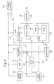
- a prior art bar code reader which includes a power source PS for supplying 5 V, a DC-DC converter 21 for changing the voltage from 5 V to 12 V, an image sensor 5 such as a CCD having 2048 pixels and operates at 12 V, an operational amplifier 9 for amplifying the output from the CCD 5, a digitalizing circuit 10 formed by an operational amplifier for changing the amplified signal to a digital signal, a level down circuit for changing the signal in the system having the Vcc of 12 V to the system having the Vcc of 5 V, and a microcomputer 14 for processing the read bar code signal.
- the microcomputer 14 includes a counter 15 for counting the width of a bar, an I/O port 16, a serial port 17, a ROM 18 and a RAM 19. By a program previously installed in the ROM 18, microcomputer 14 processes the read data and the result is applied to a buffer 20 and further transmitted to another processing device (not show).
- the bar code reader further includes a light source 2 formed by LEDs aligned in an array for emitting a ribbon of light having a wavelength of 660 nm, an image sensor drive circuit 12 for driving the CCD 5, and an indicator 13 formed by a buzzer or a lamp for indicating that the reading is completed.
- a light source 2 formed by LEDs aligned in an array for emitting a ribbon of light having a wavelength of 660 nm
- an image sensor drive circuit 12 for driving the CCD 5
- an indicator 13 formed by a buzzer or a lamp for indicating that the reading is completed.
- the image sensor 5 and circuits g, 10 and 11 operates with the operating voltage Vcc of 12 V
- the circuit 2, 12 and 13 operates with the operating voltage Vcc of 5 V.
- the former circuit is referred to as a 12 V circuit system
- the latter is referred to as a 5 V circuit system.
- DC-DC converter 21 is provided in the prior art bar code reader.
- a level down circuit 11 is necessary.
- the bar code reader becomes bulky in size, and increases the manufacturing cost. Furthermore, when a battery is used for the power source, the battery does not last long due to the use of high voltage and the power consumed in the DC-DC converter 21 and the level down circuit 11.
- the present invention has been developed with a view to substantially solving the above described disadvantages and has for its essential object to provide an improved bar code reader.
- the bar code reader comprises: the image sensor comprising light receiving elements which operates with an operating voltage Vcc less than 8 V; the amplifier comprising first and second operational amplifiers each having one voltage source terminal connected to Vcc of 5 V and the other voltage source terminal connected to ground; and the digitalizing circuit comprising a third operational amplifier having one voltage source terminal connected to Vcc of 5 V and the other voltage source terminal connected to ground.
- the bar code reader of the present invention has the image sensor which operates with an operating voltage Vcc less than 8 V and the amplifier and the digitalizing circuit that can be operated with Vcc of 5 V, it is unnecessary to provide the DC-DC converter or the level down circuit as required in the prior art bar code reader.
- the bar code reader according to the present invention can be assembled in a compact size and cost effective.
- a bar code reader according to the present invention is shown.
- a light source 2 formed by LEDs aligned in an array for emitting a ribbon of light having a wavelength of 660 nm
- a mirror 3 for guiding light reflected from a bar code 1
- an image forming lens 4 for guiding light reflected from a bar code 1
- an image forming lens 4 for guiding light reflected from a bar code 1
- an image forming lens 4 such as a CCD having 2048 pixels and operates at 5 V
- a processing circuit 6 and a communication line 7 for sending data to a terminal machine, such as a POS.
- a wireless system 7' can be used for transmitted the data, as shown in Fig. 1b.
- a photodiode for generating light (infrared light) or a wave generator for generating wave having a frequency in the range of 400 MHz can be used.
- the circuit has a power source PS for supplying 5 V, the image sensor 22, an operational amplifier 23 for amplifying the output from the CCD 22, a digitalizing circuit 23 formed by an operational amplifier for changing the amplified signal to a digital signal, and a microcomputer 14 for processing the read bar code signal.
- the microcomputer 14 includes a counter 15 for counting the width of a bar, an I/O port 16, a serial port 17, a ROM 18 and a RAM 19.
- microcomputer 14 processes the read data and the result is applied to a buffer 20 and further transmitted to another processing device (not show). From I/O port 16, shift gate pulse SH and system clocks ⁇ are applied to the drive circuit 12 which then generates and provides first clock CK1, second clock CK2, shift gate pulse SH and reset pulse RS to image sensor 22.
- the circuit further includes the light source 2, an image sensor drive circuit 12 for driving the CCD 22, and an indicator 13 formed by a buzzer or a lamp for indicating that the reading is completed.
- FIG. 3 a detailed circuit diagram of the image sensor 22, amplifier 23 and digitalizing circuit 24 is shown.
- the image sensor 22 is formed by a CCD such as TCD1201 which operates with an operating voltage Vcc of 5 V.
- the CCD receives first clock CK1, second clock CK2, shift gate pulse SH and reset pulse RS, as in the similar manner as the CCD with the operating voltage Vcc of 12 V.
- the image sensor 22 produces an image signal OS (Fig. 4a) and a compensation signal DS (Fig. 4b).
- the amplifier 23 includes a first amplifier, a second amplifier, a differential amplifier and an active filter.
- the first amplifier is defined by a transistor Tr1 and resistors r1, r2, r3 and r7.
- the second amplifier is defined by a transistor Tr2, resistors r4, r5, r6, r7', r8 and r0 and a Zener diode D3.
- the zener diode D3 has a voltage drop of 2.4 V and this voltage drop is used for setting the operating point of the operational amplifier opl.
- the transistors Tr1 and Tr2 are each arranged in an emitter follower connection.
- the differential amplifier is defined by an operational amplifier op1 and a resistor r9.
- the active filter is defined by an operational amplifier op2, resistors r10 and r11 and capacitors C1 and C2.
- the first amplifier amplifies the image signal OS and the second amplifier amplifies the compensation signal DS.
- the differential amplifier receives the amplified image signal OS and the amplified compensation signal DS and produces a difference signal (Fig. 4c) representing a difference between the signals OS and DS.
- the active filter serving as a low pass filter, receives the difference signal and cuts off high frequency noise signal which has a frequency greater than 300 KHz. Thus, the active filter produces a smoothed signal (Fig. 4d).
- the digitalizing circuit 24 includes a peak holding circuit and a differential amplifier.
- the peak holding circuit is defined by a capacitor C3, resistors r12, r13, r14 and r15 and Schottky diodes D1 and D2.
- Schottky diodes D1 and D2 are connected parallel but in opposite directions.
- the differential amplifier is defined by an operational amplifier op3 and a resistor r16.
- the peak holding circuit receives the shift gate pulse SH after each scanning operation by the image sensor 22 for resetting the digitalizing circuit 24 and determining the initial value.
- the peak holding circuit holds negative peaks and positive peaks of the smoothed signal produced from the operational amplifier op2 and produces a peak signal (Fig. 4e, dotted line) which is about 0.3 V lower or greater than the actual positive going peak point or negative going peak point, respectively.
- the operational amplifier op3 compares the smoothed signal and the peak signal and produces a binary signal (Fig. 4f) such that a HIGH level signal is produced when the smoothed signal is greater than the peak signal and a LOW level signal when the smoothed signal is smaller than the peak signal.
- the operational amplifiers op1, op2 and op3 operate with the operating voltage Vcc of 5 V. Therefore, it is unnecessary to provide the DC-DC converter or the level down circuit as provided in the prior art bar code reader.
- Each of the operational amplifiers op1, op2 and op3 has one voltage source terminal connected to Vcc of 5 V and the other voltage source terminal connected to ground so that the dynamic range of the operational amplifier can be used with full operating range.
- the amplifier 23 in Fig. 5 further has a amplitude control circuit and an offset level control circuit.
- the amplitude control circuit is defined by an operational amplifier op4, resistors r17, r18 and r19 and an analog switch SW1 controlled by microcomputer 14.
- the analog switch SW1 is a normally open switch.
- the offset level control circuit is defined by an operational amplifier op5 resistors r20, r21, r22, r23 and r24 and an analog switch SW2.
- the analog switch SW2 is a normally close switch.
- microcomputer 14 While decoding the digital signal representing the bar code in the microcomputer 14, if a decode error caused by a small amplitude of the bar code detection signal, such as shown in Fig. 6a, left-hand side, is detected, microcomputer 14 produces an ON signal along line L1 to turn switch SW1 on. Thus, a resistor r18 is connected parallel to resistor r17 to increase the amplification rate of operational amplifier op4. Thus, the bar code detection signal from operational amplifier op4 shows greater amplification, as shown in Fig. 6a, right-hand side.
- microcomputer 14 While decoding the digital signal representing the bar code in the microcomputer 14, if a decode error caused by a saturation of the bar code detection signal, such as shown in Fig. 6b, left-hand side, is detected, microcomputer 14 produces an OFF signal along line L2 to turn switch SW1 off. This may happen when the contract between the bars and spaces is relatively low. Thus, a resistor r24 is connected in series to resistor r23 to shift the operating point of the operational amplifier op5. Thus, the bar code detection signal from operational amplifier op5 is shifted within the saturation range, as shown in Fig. 6b, right-hand side.
- the ON and OFF signals from line L1 or L2 are produced in response to the shift gate pulse SH so that ON condition or OFF condition is maintained at least for one cycle between two shift gate pulses.
- a plurality of analog switches for switch SW2 can be provided to change the offset level in a plurality of different levels.
- the CCD having 2048 pixels arranged in a linear array (one dimension alignment) with operating voltage range of 4.5 to 5.5 V is employed in the image sensor 22, so as to satisfy a condition that the maximum rated operating voltage of the image sensor 22 is less than 8 V. It is possible to further reduce the operating voltage. For example, it is possible to employ a CCD which has the operating voltage of 3 V. Also, the pixel alignment in the CCD can be arranged in two dimensions instead of one dimension.
- the power source it is possible to use a dry battery or a rechargeable battery.
- the communication line 7 it is possible to use a wireless communication system, using light (infrared light) or a wave having a frequency in the range of 400 MHz.
- the bar code reader since all the circuits including the image sensor 22 has the operating voltage Vcc of 5 V, it is possible to assemble the bar code reader in a compact size, and yet the operation reliability can be improved. Also the bar code reader can be manufactured cost effective.
Abstract
Description
- The present invention relates to a bar code reader using an image sensor such as a CCD.
- In Fig. 7, a prior art bar code reader is shown which includes a power source PS for supplying 5 V, a DC-
DC converter 21 for changing the voltage from 5 V to 12 V, animage sensor 5 such as a CCD having 2048 pixels and operates at 12 V, anoperational amplifier 9 for amplifying the output from theCCD 5, a digitalizingcircuit 10 formed by an operational amplifier for changing the amplified signal to a digital signal, a level down circuit for changing the signal in the system having the Vcc of 12 V to the system having the Vcc of 5 V, and amicrocomputer 14 for processing the read bar code signal. Themicrocomputer 14 includes acounter 15 for counting the width of a bar, an I/O port 16, aserial port 17, aROM 18 and aRAM 19. By a program previously installed in theROM 18,microcomputer 14 processes the read data and the result is applied to abuffer 20 and further transmitted to another processing device (not show). - The bar code reader further includes a
light source 2 formed by LEDs aligned in an array for emitting a ribbon of light having a wavelength of 660 nm, an imagesensor drive circuit 12 for driving theCCD 5, and anindicator 13 formed by a buzzer or a lamp for indicating that the reading is completed. - In the prior art bar code reader, the
image sensor 5 and circuits g, 10 and 11 operates with the operating voltage Vcc of 12 V, and thecircuit DC converter 21 is provided in the prior art bar code reader. Furthermore, to enable the use of the signal produced in the 12 V circuit system in the 5 V circuit system, a level downcircuit 11 is necessary. - When such a DC-DC converter is employed, the bar code reader becomes bulky in size, and increases the manufacturing cost. Furthermore, when a battery is used for the power source, the battery does not last long due to the use of high voltage and the power consumed in the DC-
DC converter 21 and the level downcircuit 11. - The present invention has been developed with a view to substantially solving the above described disadvantages and has for its essential object to provide an improved bar code reader.
- In order to achieve the aforementioned object, the bar code reader according to the present invention comprises: the image sensor comprising light receiving elements which operates with an operating voltage Vcc less than 8 V; the amplifier comprising first and second operational amplifiers each having one voltage source terminal connected to Vcc of 5 V and the other voltage source terminal connected to ground; and the digitalizing circuit comprising a third operational amplifier having one voltage source terminal connected to Vcc of 5 V and the other voltage source terminal connected to ground.
- Since the bar code reader of the present invention has the image sensor which operates with an operating voltage Vcc less than 8 V and the amplifier and the digitalizing circuit that can be operated with Vcc of 5 V, it is unnecessary to provide the DC-DC converter or the level down circuit as required in the prior art bar code reader. Thus, the bar code reader according to the present invention can be assembled in a compact size and cost effective.
- These and other objects and features of the present invention will become clear from the following description taken in conjunction with the preferred embodiment thereof with reference to the accompanying drawings throughout which like parts are designated by like reference numerals, and in which:
- Figs. 1a and 1b, each is a schematic view of a bar code reader of the present invention;
- Fig. 2 is a block diagram of a bar coder reader of the present invention;
- Fig. 3 is a circuit diagram of
circuits - Figs. 4a-4f are waveform diagrams showing signals processed in the circuit of Fig. 3;
- Fig. 5 is a circuit diagram of
circuit 23 showing a modification thereof; - Figs. 6a and 6b, each is a waveform diagram showing signals processed in the circuit of Fig. 5; and
- Fig. 7 is a block diagram of a prior art bar code reader.
- Referring to Fig. 1a, a bar code reader according to the present invention is shown. Provided in a
casing 8 are alight source 2 formed by LEDs aligned in an array for emitting a ribbon of light having a wavelength of 660 nm, a mirror 3 for guiding light reflected from a bar code 1, animage forming lens 4, animage sensor 22 such as a CCD having 2048 pixels and operates at 5 V, aprocessing circuit 6, and acommunication line 7 for sending data to a terminal machine, such as a POS. Instead of thecommunication line 7, a wireless system 7' can be used for transmitted the data, as shown in Fig. 1b. For the wireless system 7', a photodiode for generating light (infrared light) or a wave generator for generating wave having a frequency in the range of 400 MHz can be used. - Referring to Fig. 2, the circuits mainly provided in the
processing circuit 6 is shown. The circuit has a power source PS for supplying 5 V, theimage sensor 22, anoperational amplifier 23 for amplifying the output from theCCD 22, a digitalizingcircuit 23 formed by an operational amplifier for changing the amplified signal to a digital signal, and amicrocomputer 14 for processing the read bar code signal. Themicrocomputer 14 includes acounter 15 for counting the width of a bar, an I/O port 16, aserial port 17, aROM 18 and aRAM 19. By a program previously installed in theROM 18,microcomputer 14 processes the read data and the result is applied to abuffer 20 and further transmitted to another processing device (not show). From I/O port 16, shift gate pulse SH and system clocks φ are applied to thedrive circuit 12 which then generates and provides first clock CK1, second clock CK2, shift gate pulse SH and reset pulse RS toimage sensor 22. - The circuit further includes the
light source 2, an imagesensor drive circuit 12 for driving theCCD 22, and anindicator 13 formed by a buzzer or a lamp for indicating that the reading is completed. - Referring to Fig. 3, a detailed circuit diagram of the
image sensor 22,amplifier 23 and digitalizingcircuit 24 is shown. - The
image sensor 22 is formed by a CCD such as TCD1201 which operates with an operating voltage Vcc of 5 V. The CCD receives first clock CK1, second clock CK2, shift gate pulse SH and reset pulse RS, as in the similar manner as the CCD with the operating voltage Vcc of 12 V. When a bar code is scanned, theimage sensor 22 produces an image signal OS (Fig. 4a) and a compensation signal DS (Fig. 4b). - The
amplifier 23 includes a first amplifier, a second amplifier, a differential amplifier and an active filter. The first amplifier is defined by a transistor Tr1 and resistors r1, r2, r3 and r7. The second amplifier is defined by a transistor Tr2, resistors r4, r5, r6, r7', r8 and r0 and a Zener diode D3. The zener diode D3 has a voltage drop of 2.4 V and this voltage drop is used for setting the operating point of the operational amplifier opl. The transistors Tr1 and Tr2 are each arranged in an emitter follower connection. The differential amplifier is defined by an operational amplifier op1 and a resistor r9. The active filter is defined by an operational amplifier op2, resistors r10 and r11 and capacitors C1 and C2. - The first amplifier amplifies the image signal OS and the second amplifier amplifies the compensation signal DS. The differential amplifier receives the amplified image signal OS and the amplified compensation signal DS and produces a difference signal (Fig. 4c) representing a difference between the signals OS and DS. The active filter, serving as a low pass filter, receives the difference signal and cuts off high frequency noise signal which has a frequency greater than 300 KHz. Thus, the active filter produces a smoothed signal (Fig. 4d).
- The digitalizing
circuit 24 includes a peak holding circuit and a differential amplifier. The peak holding circuit is defined by a capacitor C3, resistors r12, r13, r14 and r15 and Schottky diodes D1 and D2. Schottky diodes D1 and D2 are connected parallel but in opposite directions. The differential amplifier is defined by an operational amplifier op3 and a resistor r16. - The peak holding circuit receives the shift gate pulse SH after each scanning operation by the
image sensor 22 for resetting the digitalizingcircuit 24 and determining the initial value. The peak holding circuit holds negative peaks and positive peaks of the smoothed signal produced from the operational amplifier op2 and produces a peak signal (Fig. 4e, dotted line) which is about 0.3 V lower or greater than the actual positive going peak point or negative going peak point, respectively. The operational amplifier op3 compares the smoothed signal and the peak signal and produces a binary signal (Fig. 4f) such that a HIGH level signal is produced when the smoothed signal is greater than the peak signal and a LOW level signal when the smoothed signal is smaller than the peak signal. By the arrangement, the digitalizing of the read signal can be done with a high accuracy such that the binary signal changes at the edges of the bars with a high preciseness. - In the circuit shown in Fig. 3, the operational amplifiers op1, op2 and op3 operate with the operating voltage Vcc of 5 V. Therefore, it is unnecessary to provide the DC-DC converter or the level down circuit as provided in the prior art bar code reader. Each of the operational amplifiers op1, op2 and op3 has one voltage source terminal connected to Vcc of 5 V and the other voltage source terminal connected to ground so that the dynamic range of the operational amplifier can be used with full operating range.
- Referring to Fig. 5, a modification of the
amplifier 23 is shown. In addition to the circuit elements shown in Fig. 3 for theamplifier 23, theamplifier 23 in Fig. 5 further has a amplitude control circuit and an offset level control circuit. The amplitude control circuit is defined by an operational amplifier op4, resistors r17, r18 and r19 and an analog switch SW1 controlled bymicrocomputer 14. The analog switch SW1 is a normally open switch. The offset level control circuit is defined by an operational amplifier op5 resistors r20, r21, r22, r23 and r24 and an analog switch SW2. The analog switch SW2 is a normally close switch. - While decoding the digital signal representing the bar code in the
microcomputer 14, if a decode error caused by a small amplitude of the bar code detection signal, such as shown in Fig. 6a, left-hand side, is detected,microcomputer 14 produces an ON signal along line L1 to turn switch SW1 on. Thus, a resistor r18 is connected parallel to resistor r17 to increase the amplification rate of operational amplifier op4. Thus, the bar code detection signal from operational amplifier op4 shows greater amplification, as shown in Fig. 6a, right-hand side. - While decoding the digital signal representing the bar code in the
microcomputer 14, if a decode error caused by a saturation of the bar code detection signal, such as shown in Fig. 6b, left-hand side, is detected,microcomputer 14 produces an OFF signal along line L2 to turn switch SW1 off. This may happen when the contract between the bars and spaces is relatively low. Thus, a resistor r24 is connected in series to resistor r23 to shift the operating point of the operational amplifier op5. Thus, the bar code detection signal from operational amplifier op5 is shifted within the saturation range, as shown in Fig. 6b, right-hand side. - The ON and OFF signals from line L1 or L2 are produced in response to the shift gate pulse SH so that ON condition or OFF condition is maintained at least for one cycle between two shift gate pulses.
- In the example shown in Fig. 5, only one analog switch SW1 is provided for controlling the amplification rate, but a plurality of analog switches can be provided to change the amplification rate in a plurality of different steps.
- Similarly, a plurality of analog switches for switch SW2 can be provided to change the offset level in a plurality of different levels.
- In the embodiment described above, the CCD having 2048 pixels arranged in a linear array (one dimension alignment) with operating voltage range of 4.5 to 5.5 V is employed in the
image sensor 22, so as to satisfy a condition that the maximum rated operating voltage of theimage sensor 22 is less than 8 V. It is possible to further reduce the operating voltage. For example, it is possible to employ a CCD which has the operating voltage of 3 V. Also, the pixel alignment in the CCD can be arranged in two dimensions instead of one dimension. - Furthermore, for the power source, it is possible to use a dry battery or a rechargeable battery. For the
communication line 7, it is possible to use a wireless communication system, using light (infrared light) or a wave having a frequency in the range of 400 MHz. - According to the present invention, since all the circuits including the
image sensor 22 has the operating voltage Vcc of 5 V, it is possible to assemble the bar code reader in a compact size, and yet the operation reliability can be improved. Also the bar code reader can be manufactured cost effective. - Although the present invention has been fully described in connection with the preferred embodiment thereof with reference to the accompanying drawings, it is to be noted that various changes and modifications are apparent to those skilled in the art. Such changes and modifications are to be understood as included within the scope of the present invention as defined by the appended claims unless they depart therefrom.
Claims (9)
- In a bar code reader having a light source for lighting the bar code, an image sensor for receiving the reflected light from the bar code and producing an image signal, a drive circuit for driving the image sensor, an amplifier for amplifying the image signal, and a digitalizing circuit for digitalizing the amplified image signal and producing a digital signal representing the bar code, an improvement comprising:
said image sensor comprising light receiving elements which operates with an operating voltage Vcc less than 8 V;
said amplifier comprising first and second operational amplifiers each having one voltage source terminal connected to Vcc of 5 V and the other voltage source terminal connected to ground; and
said digitalizing circuit comprising a third operational amplifier having one voltage source terminal connected to Vcc of 5 V and the other voltage source terminal connected to ground. - A bar code reader as claimed in Claim 1, wherein said light receiving elements are formed in a CCD.
- A bar code reader as claimed in Claim 1, wherein said digitalizing circuit is reset after each scanning operation of said image sensor.
- A bar code reader as claimed in Claim 1, further comprising an amplitude control means for controlling the amplitude of the signal produced from said amplifier.
- A bar code reader as claimed in Claim 1, further comprising an offset level control means for controlling the offset level of the signal produced from said amplifier.
- A bar code reader as claimed in Claim 1, further comprising a processor 14 for decoding the digital signal.
- A bar code reader as claimed in Claim 6, further comprising a data communication system for transmitting the decoded digital signal.
- A bar code reader as claimed in Claim 7, wherein said data communication system is a wireless system comprising a photodiode.
- A bar code reader as claimed in Claim 7, wherein said data communication system is a wireless system comprising a wave generator.
Applications Claiming Priority (3)
| Application Number | Priority Date | Filing Date | Title |
|---|---|---|---|
| JP3187357A JP2720641B2 (en) | 1991-07-26 | 1991-07-26 | Barcode reader |
| JP187357/91 | 1991-07-26 | ||
| JP18735791 | 1991-07-26 |
Publications (3)
| Publication Number | Publication Date |
|---|---|
| EP0524653A2 true EP0524653A2 (en) | 1993-01-27 |
| EP0524653A3 EP0524653A3 (en) | 1993-08-18 |
| EP0524653B1 EP0524653B1 (en) | 2000-03-29 |
Family
ID=16204584
Family Applications (1)
| Application Number | Title | Priority Date | Filing Date |
|---|---|---|---|
| EP92112740A Expired - Lifetime EP0524653B1 (en) | 1991-07-26 | 1992-07-25 | Bar code reader |
Country Status (5)
| Country | Link |
|---|---|
| US (1) | US5349171A (en) |
| EP (1) | EP0524653B1 (en) |
| JP (1) | JP2720641B2 (en) |
| CA (1) | CA2074653C (en) |
| DE (1) | DE69230846T2 (en) |
Cited By (2)
| Publication number | Priority date | Publication date | Assignee | Title |
|---|---|---|---|---|
| WO1993017397A1 (en) * | 1992-02-27 | 1993-09-02 | Alex Roustaei | Optical scanning head |
| US5756981A (en) * | 1992-02-27 | 1998-05-26 | Symbol Technologies, Inc. | Optical scanner for reading and decoding one- and-two-dimensional symbologies at variable depths of field including memory efficient high speed image processing means and high accuracy image analysis means |
Families Citing this family (4)
| Publication number | Priority date | Publication date | Assignee | Title |
|---|---|---|---|---|
| JPH0830715A (en) * | 1994-07-15 | 1996-02-02 | Tec Corp | Code reader |
| JP3470420B2 (en) * | 1994-11-14 | 2003-11-25 | ソニー株式会社 | Output circuit having a binarization circuit |
| AU2002234688A1 (en) * | 2002-01-30 | 2003-09-04 | Francois Duret | Electro-optical device for the photo-polymerization of composite material |
| RU2710692C2 (en) * | 2015-08-14 | 2020-01-09 | Филип Моррис Продактс С.А. | Electrically operated smoking device comprising smoking articles identification system in such device |
Citations (5)
| Publication number | Priority date | Publication date | Assignee | Title |
|---|---|---|---|---|
| EP0094571A2 (en) * | 1982-05-19 | 1983-11-23 | Msi Data Corporation | Self-contained portable data entry terminal |
| JPS62179072A (en) * | 1986-02-03 | 1987-08-06 | Matsushita Electric Ind Co Ltd | Bar code reader |
| EP0287913A2 (en) * | 1987-04-22 | 1988-10-26 | Abbott Laboratories | Optical code reader and format |
| US4870262A (en) * | 1987-01-06 | 1989-09-26 | Alps Electric Co., Ltd. | Signal processing apparatus and binary encoder circuit for the same |
| US4902883A (en) * | 1988-01-28 | 1990-02-20 | Hewlett-Packard Company | Digitized video signal and time interval measurement transmission from a bar code reader |
Family Cites Families (5)
| Publication number | Priority date | Publication date | Assignee | Title |
|---|---|---|---|---|
| US4140271A (en) * | 1975-04-17 | 1979-02-20 | Nippondenso Co., Ltd. | Method and apparatus to read in bar-coded information |
| JPS5331920A (en) * | 1976-09-06 | 1978-03-25 | Nippon Denso Co Ltd | Bar code reader |
| JPS57152074A (en) * | 1981-03-16 | 1982-09-20 | Nippon Denso Co Ltd | Bar code reader |
| JP2870046B2 (en) * | 1989-09-29 | 1999-03-10 | 日本電気株式会社 | Charge-coupled device |
| JPH0574876A (en) * | 1991-09-12 | 1993-03-26 | Ricoh Co Ltd | Wire bonder |
-
1991
- 1991-07-26 JP JP3187357A patent/JP2720641B2/en not_active Expired - Lifetime
-
1992
- 1992-07-24 CA CA002074653A patent/CA2074653C/en not_active Expired - Fee Related
- 1992-07-25 EP EP92112740A patent/EP0524653B1/en not_active Expired - Lifetime
- 1992-07-25 DE DE69230846T patent/DE69230846T2/en not_active Expired - Fee Related
- 1992-07-27 US US07/919,906 patent/US5349171A/en not_active Expired - Lifetime
Patent Citations (5)
| Publication number | Priority date | Publication date | Assignee | Title |
|---|---|---|---|---|
| EP0094571A2 (en) * | 1982-05-19 | 1983-11-23 | Msi Data Corporation | Self-contained portable data entry terminal |
| JPS62179072A (en) * | 1986-02-03 | 1987-08-06 | Matsushita Electric Ind Co Ltd | Bar code reader |
| US4870262A (en) * | 1987-01-06 | 1989-09-26 | Alps Electric Co., Ltd. | Signal processing apparatus and binary encoder circuit for the same |
| EP0287913A2 (en) * | 1987-04-22 | 1988-10-26 | Abbott Laboratories | Optical code reader and format |
| US4902883A (en) * | 1988-01-28 | 1990-02-20 | Hewlett-Packard Company | Digitized video signal and time interval measurement transmission from a bar code reader |
Non-Patent Citations (1)
| Title |
|---|
| ELEKTOR vol. 7, no. 5, May 1981, CANTERBURY,KENT,GR.BRITAIN pages 5-43 - 5-49 HEWLETT-PACKARD JOURNAL 'READING BAR CODES' * |
Cited By (2)
| Publication number | Priority date | Publication date | Assignee | Title |
|---|---|---|---|---|
| WO1993017397A1 (en) * | 1992-02-27 | 1993-09-02 | Alex Roustaei | Optical scanning head |
| US5756981A (en) * | 1992-02-27 | 1998-05-26 | Symbol Technologies, Inc. | Optical scanner for reading and decoding one- and-two-dimensional symbologies at variable depths of field including memory efficient high speed image processing means and high accuracy image analysis means |
Also Published As
| Publication number | Publication date |
|---|---|
| EP0524653B1 (en) | 2000-03-29 |
| US5349171A (en) | 1994-09-20 |
| JP2720641B2 (en) | 1998-03-04 |
| DE69230846D1 (en) | 2000-05-04 |
| JPH0535905A (en) | 1993-02-12 |
| DE69230846T2 (en) | 2000-11-16 |
| CA2074653A1 (en) | 1993-01-27 |
| EP0524653A3 (en) | 1993-08-18 |
| CA2074653C (en) | 1996-07-16 |
Similar Documents
| Publication | Publication Date | Title |
|---|---|---|
| US4538060A (en) | Optical reading apparatus having a reading sensor of electronic scanning type | |
| US4874933A (en) | Ambient illumination bar code reader | |
| EP0085495B1 (en) | High-sensitive optical reading apparatus and method of reading optical information | |
| US4356389A (en) | Bar code scanner interface | |
| US5168148A (en) | Automatic gain control circuit | |
| EP0193762B1 (en) | Low powered high ambient light bar code reader circuit | |
| JPH0650535B2 (en) | Optical information reader | |
| US5654533A (en) | Apparatus and method for reading two-dimensional symbols | |
| US5349171A (en) | Bar code reader | |
| JP2748263B2 (en) | Barcode reader and image sensor used for it | |
| KR0177977B1 (en) | Detection apparatus of minimum/maximum value of diaphragm of switch lens using bar code | |
| JPH04223583A (en) | Bar code reader | |
| JP2748721B2 (en) | Barcode reader | |
| JP2843477B2 (en) | Optical signal input type amplifier circuit | |
| JPS63198177A (en) | Optical reader | |
| US4177449A (en) | Photoelectric converter apparatus | |
| JPS63225884A (en) | Optical information reader | |
| JPH08153153A (en) | Optical information reader | |
| JPH0693748B2 (en) | Shading correction circuit for image sensor | |
| JP2729449B2 (en) | Optical information reader | |
| US7474347B2 (en) | Solid-state image pickup device having a lensing function | |
| JPS6159573A (en) | Noise removing circuit of bar signal in bar code reader | |
| JPH0428033Y2 (en) | ||
| JPS63276680A (en) | Bar code reader | |
| JPH01175685A (en) | Method for adjusting resolution of bar code reader |
Legal Events
| Date | Code | Title | Description |
|---|---|---|---|
| PUAI | Public reference made under article 153(3) epc to a published international application that has entered the european phase |
Free format text: ORIGINAL CODE: 0009012 |
|
| 17P | Request for examination filed |
Effective date: 19920725 |
|
| AK | Designated contracting states |
Kind code of ref document: A2 Designated state(s): DE FR GB IT |
|
| PUAL | Search report despatched |
Free format text: ORIGINAL CODE: 0009013 |
|
| AK | Designated contracting states |
Kind code of ref document: A3 Designated state(s): DE FR GB IT |
|
| 17Q | First examination report despatched |
Effective date: 19960116 |
|
| GRAG | Despatch of communication of intention to grant |
Free format text: ORIGINAL CODE: EPIDOS AGRA |
|
| GRAG | Despatch of communication of intention to grant |
Free format text: ORIGINAL CODE: EPIDOS AGRA |
|
| GRAH | Despatch of communication of intention to grant a patent |
Free format text: ORIGINAL CODE: EPIDOS IGRA |
|
| GRAH | Despatch of communication of intention to grant a patent |
Free format text: ORIGINAL CODE: EPIDOS IGRA |
|
| GRAA | (expected) grant |
Free format text: ORIGINAL CODE: 0009210 |
|
| AK | Designated contracting states |
Kind code of ref document: B1 Designated state(s): DE FR GB IT |
|
| ITF | It: translation for a ep patent filed |
Owner name: JACOBACCI & PERANI S.P.A. |
|
| REF | Corresponds to: |
Ref document number: 69230846 Country of ref document: DE Date of ref document: 20000504 |
|
| ET | Fr: translation filed | ||
| PLBE | No opposition filed within time limit |
Free format text: ORIGINAL CODE: 0009261 |
|
| STAA | Information on the status of an ep patent application or granted ep patent |
Free format text: STATUS: NO OPPOSITION FILED WITHIN TIME LIMIT |
|
| 26N | No opposition filed | ||
| REG | Reference to a national code |
Ref country code: GB Ref legal event code: IF02 |
|
| PGFP | Annual fee paid to national office [announced via postgrant information from national office to epo] |
Ref country code: DE Payment date: 20080807 Year of fee payment: 17 |
|
| PGFP | Annual fee paid to national office [announced via postgrant information from national office to epo] |
Ref country code: FR Payment date: 20080718 Year of fee payment: 17 Ref country code: IT Payment date: 20080731 Year of fee payment: 17 |
|
| PGFP | Annual fee paid to national office [announced via postgrant information from national office to epo] |
Ref country code: GB Payment date: 20080806 Year of fee payment: 17 |
|
| GBPC | Gb: european patent ceased through non-payment of renewal fee |
Effective date: 20090725 |
|
| REG | Reference to a national code |
Ref country code: FR Ref legal event code: ST Effective date: 20100331 |
|
| PG25 | Lapsed in a contracting state [announced via postgrant information from national office to epo] |
Ref country code: FR Free format text: LAPSE BECAUSE OF NON-PAYMENT OF DUE FEES Effective date: 20090731 |
|
| PG25 | Lapsed in a contracting state [announced via postgrant information from national office to epo] |
Ref country code: GB Free format text: LAPSE BECAUSE OF NON-PAYMENT OF DUE FEES Effective date: 20090725 |
|
| PG25 | Lapsed in a contracting state [announced via postgrant information from national office to epo] |
Ref country code: DE Free format text: LAPSE BECAUSE OF NON-PAYMENT OF DUE FEES Effective date: 20100202 |
|
| PG25 | Lapsed in a contracting state [announced via postgrant information from national office to epo] |
Ref country code: IT Free format text: LAPSE BECAUSE OF NON-PAYMENT OF DUE FEES Effective date: 20090725 |