EP0528662A1 - Organic field effect transistor - Google Patents
Organic field effect transistor Download PDFInfo
- Publication number
- EP0528662A1 EP0528662A1 EP92307470A EP92307470A EP0528662A1 EP 0528662 A1 EP0528662 A1 EP 0528662A1 EP 92307470 A EP92307470 A EP 92307470A EP 92307470 A EP92307470 A EP 92307470A EP 0528662 A1 EP0528662 A1 EP 0528662A1
- Authority
- EP
- European Patent Office
- Prior art keywords
- organic layer
- element according
- channel
- organic
- compound
- Prior art date
- Legal status (The legal status is an assumption and is not a legal conclusion. Google has not performed a legal analysis and makes no representation as to the accuracy of the status listed.)
- Granted
Links
- 230000005669 field effect Effects 0.000 title claims abstract description 46
- 239000012044 organic layer Substances 0.000 claims abstract description 114
- 239000000969 carrier Substances 0.000 claims abstract description 38
- 230000004044 response Effects 0.000 claims abstract description 11
- 230000008859 change Effects 0.000 claims abstract description 7
- 239000010410 layer Substances 0.000 claims description 53
- -1 polyparaphenylene Polymers 0.000 claims description 42
- 229920000547 conjugated polymer Polymers 0.000 claims description 38
- 239000000463 material Substances 0.000 claims description 38
- 239000004973 liquid crystal related substance Substances 0.000 claims description 25
- 239000000758 substrate Substances 0.000 claims description 21
- 229920000642 polymer Chemical class 0.000 claims description 14
- 239000004065 semiconductor Substances 0.000 claims description 13
- 239000002019 doping agent Substances 0.000 claims description 10
- 125000000217 alkyl group Chemical group 0.000 claims description 8
- 229910052751 metal Inorganic materials 0.000 claims description 8
- 239000002184 metal Substances 0.000 claims description 8
- 239000000049 pigment Substances 0.000 claims description 8
- IEQIEDJGQAUEQZ-UHFFFAOYSA-N phthalocyanine Chemical compound N1C(N=C2C3=CC=CC=C3C(N=C3C4=CC=CC=C4C(=N4)N3)=N2)=C(C=CC=C2)C2=C1N=C1C2=CC=CC=C2C4=N1 IEQIEDJGQAUEQZ-UHFFFAOYSA-N 0.000 claims description 6
- 229920000548 poly(silane) polymer Polymers 0.000 claims description 6
- 229920000265 Polyparaphenylene Polymers 0.000 claims description 5
- 229920000128 polypyrrole Polymers 0.000 claims description 4
- 150000001450 anions Chemical class 0.000 claims description 3
- UJOBWOGCFQCDNV-UHFFFAOYSA-N Carbazole Natural products C1=CC=C2C3=CC=CC=C3NC2=C1 UJOBWOGCFQCDNV-UHFFFAOYSA-N 0.000 claims description 2
- 239000002841 Lewis acid Substances 0.000 claims description 2
- 239000004721 Polyphenylene oxide Substances 0.000 claims description 2
- 239000004734 Polyphenylene sulfide Substances 0.000 claims description 2
- PJANXHGTPQOBST-VAWYXSNFSA-N Stilbene Natural products C=1C=CC=CC=1/C=C/C1=CC=CC=C1 PJANXHGTPQOBST-VAWYXSNFSA-N 0.000 claims description 2
- OIPILFWXSMYKGL-UHFFFAOYSA-N acetylcholine Chemical compound CC(=O)OCC[N+](C)(C)C OIPILFWXSMYKGL-UHFFFAOYSA-N 0.000 claims description 2
- 229960004373 acetylcholine Drugs 0.000 claims description 2
- 239000002253 acid Substances 0.000 claims description 2
- 229910052783 alkali metal Inorganic materials 0.000 claims description 2
- 150000001340 alkali metals Chemical class 0.000 claims description 2
- 229910052784 alkaline earth metal Inorganic materials 0.000 claims description 2
- 150000001342 alkaline earth metals Chemical class 0.000 claims description 2
- HSFWRNGVRCDJHI-UHFFFAOYSA-N alpha-acetylene Natural products C#C HSFWRNGVRCDJHI-UHFFFAOYSA-N 0.000 claims description 2
- 150000001413 amino acids Chemical class 0.000 claims description 2
- 239000000987 azo dye Substances 0.000 claims description 2
- 150000001768 cations Chemical class 0.000 claims description 2
- 150000001875 compounds Chemical class 0.000 claims description 2
- 229910052736 halogen Inorganic materials 0.000 claims description 2
- 150000002367 halogens Chemical class 0.000 claims description 2
- 150000007517 lewis acids Chemical class 0.000 claims description 2
- 150000007524 organic acids Chemical class 0.000 claims description 2
- 229920003227 poly(N-vinyl carbazole) Polymers 0.000 claims description 2
- 229920001197 polyacetylene Polymers 0.000 claims description 2
- 229920000767 polyaniline Polymers 0.000 claims description 2
- 229920000323 polyazulene Polymers 0.000 claims description 2
- 125000003367 polycyclic group Chemical group 0.000 claims description 2
- 229920002098 polyfluorene Polymers 0.000 claims description 2
- 229920000414 polyfuran Polymers 0.000 claims description 2
- 229920006380 polyphenylene oxide Polymers 0.000 claims description 2
- 229920000069 polyphenylene sulfide Polymers 0.000 claims description 2
- 229920000123 polythiophene Polymers 0.000 claims description 2
- 235000021286 stilbenes Nutrition 0.000 claims description 2
- 150000003623 transition metal compounds Chemical class 0.000 claims description 2
- KAKZBPTYRLMSJV-UHFFFAOYSA-N vinyl-ethylene Natural products C=CC=C KAKZBPTYRLMSJV-UHFFFAOYSA-N 0.000 claims description 2
- 238000000034 method Methods 0.000 description 25
- YXFVVABEGXRONW-UHFFFAOYSA-N Toluene Chemical compound CC1=CC=CC=C1 YXFVVABEGXRONW-UHFFFAOYSA-N 0.000 description 9
- 239000000975 dye Substances 0.000 description 9
- 239000011521 glass Substances 0.000 description 9
- 239000010408 film Substances 0.000 description 8
- 239000010409 thin film Substances 0.000 description 8
- 239000011230 binding agent Substances 0.000 description 7
- 239000000243 solution Substances 0.000 description 7
- 239000011159 matrix material Substances 0.000 description 6
- 238000000576 coating method Methods 0.000 description 5
- 230000003247 decreasing effect Effects 0.000 description 5
- 239000003054 catalyst Substances 0.000 description 4
- 238000006116 polymerization reaction Methods 0.000 description 4
- WEVYAHXRMPXWCK-UHFFFAOYSA-N Acetonitrile Chemical compound CC#N WEVYAHXRMPXWCK-UHFFFAOYSA-N 0.000 description 3
- 238000000151 deposition Methods 0.000 description 3
- 230000005684 electric field Effects 0.000 description 3
- 239000013034 phenoxy resin Substances 0.000 description 3
- 229920006287 phenoxy resin Polymers 0.000 description 3
- QGZKDVFQNNGYKY-UHFFFAOYSA-N Ammonia Chemical compound N QGZKDVFQNNGYKY-UHFFFAOYSA-N 0.000 description 2
- LFQSCWFLJHTTHZ-UHFFFAOYSA-N Ethanol Chemical compound CCO LFQSCWFLJHTTHZ-UHFFFAOYSA-N 0.000 description 2
- 239000004642 Polyimide Substances 0.000 description 2
- KAESVJOAVNADME-UHFFFAOYSA-N Pyrrole Chemical compound C=1C=CNC=1 KAESVJOAVNADME-UHFFFAOYSA-N 0.000 description 2
- BUGBHKTXTAQXES-UHFFFAOYSA-N Selenium Chemical compound [Se] BUGBHKTXTAQXES-UHFFFAOYSA-N 0.000 description 2
- 229910021417 amorphous silicon Inorganic materials 0.000 description 2
- ILAHWRKJUDSMFH-UHFFFAOYSA-N boron tribromide Chemical compound BrB(Br)Br ILAHWRKJUDSMFH-UHFFFAOYSA-N 0.000 description 2
- 238000006243 chemical reaction Methods 0.000 description 2
- 239000011248 coating agent Substances 0.000 description 2
- 230000008021 deposition Effects 0.000 description 2
- 238000010586 diagram Methods 0.000 description 2
- 238000007606 doctor blade method Methods 0.000 description 2
- 238000012685 gas phase polymerization Methods 0.000 description 2
- 238000007654 immersion Methods 0.000 description 2
- 239000012212 insulator Substances 0.000 description 2
- 239000007788 liquid Substances 0.000 description 2
- 239000000178 monomer Substances 0.000 description 2
- 239000011368 organic material Substances 0.000 description 2
- 239000003960 organic solvent Substances 0.000 description 2
- 229920003023 plastic Polymers 0.000 description 2
- 239000004033 plastic Substances 0.000 description 2
- 229920000728 polyester Polymers 0.000 description 2
- 229920001721 polyimide Polymers 0.000 description 2
- 230000000379 polymerizing effect Effects 0.000 description 2
- 230000008569 process Effects 0.000 description 2
- 229920005989 resin Polymers 0.000 description 2
- 239000011347 resin Substances 0.000 description 2
- 238000012552 review Methods 0.000 description 2
- 238000007761 roller coating Methods 0.000 description 2
- 239000002904 solvent Substances 0.000 description 2
- 238000004528 spin coating Methods 0.000 description 2
- AKEJUJNQAAGONA-UHFFFAOYSA-N sulfur trioxide Chemical compound O=S(=O)=O AKEJUJNQAAGONA-UHFFFAOYSA-N 0.000 description 2
- 230000007704 transition Effects 0.000 description 2
- 238000001771 vacuum deposition Methods 0.000 description 2
- XLYOFNOQVPJJNP-UHFFFAOYSA-N water Chemical compound O XLYOFNOQVPJJNP-UHFFFAOYSA-N 0.000 description 2
- UOCLXMDMGBRAIB-UHFFFAOYSA-N 1,1,1-trichloroethane Chemical compound CC(Cl)(Cl)Cl UOCLXMDMGBRAIB-UHFFFAOYSA-N 0.000 description 1
- FKNIDKXOANSRCS-UHFFFAOYSA-N 2,3,4-trinitrofluoren-1-one Chemical compound C1=CC=C2C3=C([N+](=O)[O-])C([N+]([O-])=O)=C([N+]([O-])=O)C(=O)C3=CC2=C1 FKNIDKXOANSRCS-UHFFFAOYSA-N 0.000 description 1
- KXGFMDJXCMQABM-UHFFFAOYSA-N 2-methoxy-6-methylphenol Chemical compound [CH]OC1=CC=CC([CH])=C1O KXGFMDJXCMQABM-UHFFFAOYSA-N 0.000 description 1
- ZCYVEMRRCGMTRW-UHFFFAOYSA-N 7553-56-2 Chemical compound [I] ZCYVEMRRCGMTRW-UHFFFAOYSA-N 0.000 description 1
- 239000004925 Acrylic resin Substances 0.000 description 1
- 229920000178 Acrylic resin Polymers 0.000 description 1
- 229910021630 Antimony pentafluoride Inorganic materials 0.000 description 1
- 229910017049 AsF5 Inorganic materials 0.000 description 1
- 229910015845 BBr3 Inorganic materials 0.000 description 1
- 229910015844 BCl3 Inorganic materials 0.000 description 1
- 229910015900 BF3 Inorganic materials 0.000 description 1
- BVKZGUZCCUSVTD-UHFFFAOYSA-L Carbonate Chemical compound [O-]C([O-])=O BVKZGUZCCUSVTD-UHFFFAOYSA-L 0.000 description 1
- RWSOTUBLDIXVET-UHFFFAOYSA-N Dihydrogen sulfide Chemical class S RWSOTUBLDIXVET-UHFFFAOYSA-N 0.000 description 1
- 229910005185 FSO3H Inorganic materials 0.000 description 1
- 229910003865 HfCl4 Inorganic materials 0.000 description 1
- VEXZGXHMUGYJMC-UHFFFAOYSA-N Hydrochloric acid Chemical compound Cl VEXZGXHMUGYJMC-UHFFFAOYSA-N 0.000 description 1
- 229910021578 Iron(III) chloride Inorganic materials 0.000 description 1
- 229910002422 La(NO3)3·6H2O Inorganic materials 0.000 description 1
- 229910015221 MoCl5 Inorganic materials 0.000 description 1
- 229910015253 MoF5 Inorganic materials 0.000 description 1
- 229910019804 NbCl5 Inorganic materials 0.000 description 1
- 229910019787 NbF5 Inorganic materials 0.000 description 1
- GRYLNZFGIOXLOG-UHFFFAOYSA-N Nitric acid Chemical compound O[N+]([O-])=O GRYLNZFGIOXLOG-UHFFFAOYSA-N 0.000 description 1
- 229910021174 PF5 Inorganic materials 0.000 description 1
- NRCMAYZCPIVABH-UHFFFAOYSA-N Quinacridone Chemical compound N1C2=CC=CC=C2C(=O)C2=C1C=C1C(=O)C3=CC=CC=C3NC1=C2 NRCMAYZCPIVABH-UHFFFAOYSA-N 0.000 description 1
- 229910001370 Se alloy Inorganic materials 0.000 description 1
- QAOWNCQODCNURD-UHFFFAOYSA-N Sulfuric acid Chemical compound OS(O)(=O)=O QAOWNCQODCNURD-UHFFFAOYSA-N 0.000 description 1
- 229910004537 TaCl5 Inorganic materials 0.000 description 1
- 229910003074 TiCl4 Inorganic materials 0.000 description 1
- 229920002433 Vinyl chloride-vinyl acetate copolymer Polymers 0.000 description 1
- 229910003091 WCl6 Inorganic materials 0.000 description 1
- 229910009035 WF6 Inorganic materials 0.000 description 1
- 229910007932 ZrCl4 Inorganic materials 0.000 description 1
- DHKHKXVYLBGOIT-UHFFFAOYSA-N acetaldehyde Diethyl Acetal Natural products CCOC(C)OCC DHKHKXVYLBGOIT-UHFFFAOYSA-N 0.000 description 1
- 125000002777 acetyl group Chemical class [H]C([H])([H])C(*)=O 0.000 description 1
- 150000007513 acids Chemical class 0.000 description 1
- 229920000180 alkyd Polymers 0.000 description 1
- 229910021529 ammonia Inorganic materials 0.000 description 1
- 150000008064 anhydrides Chemical class 0.000 description 1
- PYKYMHQGRFAEBM-UHFFFAOYSA-N anthraquinone Natural products CCC(=O)c1c(O)c2C(=O)C3C(C=CC=C3O)C(=O)c2cc1CC(=O)OC PYKYMHQGRFAEBM-UHFFFAOYSA-N 0.000 description 1
- 150000004056 anthraquinones Chemical class 0.000 description 1
- VBVBHWZYQGJZLR-UHFFFAOYSA-I antimony pentafluoride Chemical compound F[Sb](F)(F)(F)F VBVBHWZYQGJZLR-UHFFFAOYSA-I 0.000 description 1
- YBGKQGSCGDNZIB-UHFFFAOYSA-N arsenic pentafluoride Chemical compound F[As](F)(F)(F)F YBGKQGSCGDNZIB-UHFFFAOYSA-N 0.000 description 1
- 239000012298 atmosphere Substances 0.000 description 1
- WTEOIRVLGSZEPR-UHFFFAOYSA-N boron trifluoride Chemical compound FB(F)F WTEOIRVLGSZEPR-UHFFFAOYSA-N 0.000 description 1
- 229910052794 bromium Inorganic materials 0.000 description 1
- 125000000484 butyl group Chemical group [H]C([*])([H])C([H])([H])C([H])([H])C([H])([H])[H] 0.000 description 1
- UHYPYGJEEGLRJD-UHFFFAOYSA-N cadmium(2+);selenium(2-) Chemical compound [Se-2].[Cd+2] UHYPYGJEEGLRJD-UHFFFAOYSA-N 0.000 description 1
- 229910052792 caesium Inorganic materials 0.000 description 1
- 229910052791 calcium Inorganic materials 0.000 description 1
- 230000008602 contraction Effects 0.000 description 1
- 210000002858 crystal cell Anatomy 0.000 description 1
- 239000008367 deionised water Substances 0.000 description 1
- 229910021641 deionized water Inorganic materials 0.000 description 1
- 125000000664 diazo group Chemical group [N-]=[N+]=[*] 0.000 description 1
- GNEPOXWQWFSSOU-UHFFFAOYSA-N dichloro-methyl-phenylsilane Chemical compound C[Si](Cl)(Cl)C1=CC=CC=C1 GNEPOXWQWFSSOU-UHFFFAOYSA-N 0.000 description 1
- 239000000539 dimer Substances 0.000 description 1
- 239000012153 distilled water Substances 0.000 description 1
- 239000003792 electrolyte Substances 0.000 description 1
- 238000000313 electron-beam-induced deposition Methods 0.000 description 1
- UQSQSQZYBQSBJZ-UHFFFAOYSA-N fluorosulfonic acid Chemical compound OS(F)(=O)=O UQSQSQZYBQSBJZ-UHFFFAOYSA-N 0.000 description 1
- PDPJQWYGJJBYLF-UHFFFAOYSA-J hafnium tetrachloride Chemical compound Cl[Hf](Cl)(Cl)Cl PDPJQWYGJJBYLF-UHFFFAOYSA-J 0.000 description 1
- 150000003949 imides Chemical class 0.000 description 1
- 238000002347 injection Methods 0.000 description 1
- 239000007924 injection Substances 0.000 description 1
- 239000002198 insoluble material Substances 0.000 description 1
- 239000011810 insulating material Substances 0.000 description 1
- 229910052740 iodine Inorganic materials 0.000 description 1
- 239000011630 iodine Substances 0.000 description 1
- 150000002500 ions Chemical class 0.000 description 1
- RBTARNINKXHZNM-UHFFFAOYSA-K iron trichloride Chemical compound Cl[Fe](Cl)Cl RBTARNINKXHZNM-UHFFFAOYSA-K 0.000 description 1
- 229910052747 lanthanoid Inorganic materials 0.000 description 1
- 150000002602 lanthanoids Chemical class 0.000 description 1
- 229910052744 lithium Inorganic materials 0.000 description 1
- 229910052749 magnesium Inorganic materials 0.000 description 1
- 238000004519 manufacturing process Methods 0.000 description 1
- 150000002739 metals Chemical class 0.000 description 1
- NYGZLYXAPMMJTE-UHFFFAOYSA-M metanil yellow Chemical group [Na+].[O-]S(=O)(=O)C1=CC=CC(N=NC=2C=CC(NC=3C=CC=CC=3)=CC=2)=C1 NYGZLYXAPMMJTE-UHFFFAOYSA-M 0.000 description 1
- 125000002496 methyl group Chemical group [H]C([H])([H])* 0.000 description 1
- 239000000203 mixture Substances 0.000 description 1
- GICWIDZXWJGTCI-UHFFFAOYSA-I molybdenum pentachloride Chemical compound Cl[Mo](Cl)(Cl)(Cl)Cl GICWIDZXWJGTCI-UHFFFAOYSA-I 0.000 description 1
- NBJFDNVXVFBQDX-UHFFFAOYSA-I molybdenum pentafluoride Chemical compound F[Mo](F)(F)(F)F NBJFDNVXVFBQDX-UHFFFAOYSA-I 0.000 description 1
- 229910052759 nickel Inorganic materials 0.000 description 1
- 229910017604 nitric acid Inorganic materials 0.000 description 1
- 235000005985 organic acids Nutrition 0.000 description 1
- SJHHDDDGXWOYOE-UHFFFAOYSA-N oxytitamium phthalocyanine Chemical compound [Ti+2]=O.C12=CC=CC=C2C(N=C2[N-]C(C3=CC=CC=C32)=N2)=NC1=NC([C]1C=CC=CC1=1)=NC=1N=C1[C]3C=CC=CC3=C2[N-]1 SJHHDDDGXWOYOE-UHFFFAOYSA-N 0.000 description 1
- YRZZLAGRKZIJJI-UHFFFAOYSA-N oxyvanadium phthalocyanine Chemical compound [V+2]=O.C12=CC=CC=C2C(N=C2[N-]C(C3=CC=CC=C32)=N2)=NC1=NC([C]1C=CC=CC1=1)=NC=1N=C1[C]3C=CC=CC3=C2[N-]1 YRZZLAGRKZIJJI-UHFFFAOYSA-N 0.000 description 1
- 239000002245 particle Substances 0.000 description 1
- YHBDIEWMOMLKOO-UHFFFAOYSA-I pentachloroniobium Chemical compound Cl[Nb](Cl)(Cl)(Cl)Cl YHBDIEWMOMLKOO-UHFFFAOYSA-I 0.000 description 1
- AOLPZAHRYHXPLR-UHFFFAOYSA-I pentafluoroniobium Chemical compound F[Nb](F)(F)(F)F AOLPZAHRYHXPLR-UHFFFAOYSA-I 0.000 description 1
- VLTRZXGMWDSKGL-UHFFFAOYSA-N perchloric acid Chemical compound OCl(=O)(=O)=O VLTRZXGMWDSKGL-UHFFFAOYSA-N 0.000 description 1
- 239000005011 phenolic resin Substances 0.000 description 1
- 229920001568 phenolic resin Polymers 0.000 description 1
- 125000001997 phenyl group Chemical group [H]C1=C([H])C([H])=C(*)C([H])=C1[H] 0.000 description 1
- OBCUTHMOOONNBS-UHFFFAOYSA-N phosphorus pentafluoride Chemical compound FP(F)(F)(F)F OBCUTHMOOONNBS-UHFFFAOYSA-N 0.000 description 1
- 238000005268 plasma chemical vapour deposition Methods 0.000 description 1
- 229920002037 poly(vinyl butyral) polymer Polymers 0.000 description 1
- 229920001230 polyarylate Polymers 0.000 description 1
- 239000004417 polycarbonate Substances 0.000 description 1
- 229920000515 polycarbonate Polymers 0.000 description 1
- 229920005668 polycarbonate resin Polymers 0.000 description 1
- 239000004431 polycarbonate resin Substances 0.000 description 1
- 229920006254 polymer film Polymers 0.000 description 1
- 229920001296 polysiloxane Polymers 0.000 description 1
- 229920002689 polyvinyl acetate Polymers 0.000 description 1
- 239000011118 polyvinyl acetate Substances 0.000 description 1
- 239000004800 polyvinyl chloride Substances 0.000 description 1
- 229920000915 polyvinyl chloride Polymers 0.000 description 1
- 229910052700 potassium Inorganic materials 0.000 description 1
- 229910052701 rubidium Inorganic materials 0.000 description 1
- 229910052711 selenium Inorganic materials 0.000 description 1
- 239000011669 selenium Substances 0.000 description 1
- 230000035939 shock Effects 0.000 description 1
- 229910052708 sodium Inorganic materials 0.000 description 1
- 239000007787 solid Substances 0.000 description 1
- 239000012265 solid product Substances 0.000 description 1
- 239000007921 spray Substances 0.000 description 1
- 238000005507 spraying Methods 0.000 description 1
- 238000004544 sputter deposition Methods 0.000 description 1
- 229910052712 strontium Inorganic materials 0.000 description 1
- 229920001909 styrene-acrylic polymer Polymers 0.000 description 1
- 150000003460 sulfonic acids Chemical class 0.000 description 1
- XTHPWXDJESJLNJ-UHFFFAOYSA-N sulfurochloridic acid Chemical compound OS(Cl)(=O)=O XTHPWXDJESJLNJ-UHFFFAOYSA-N 0.000 description 1
- 235000011149 sulphuric acid Nutrition 0.000 description 1
- 229910052715 tantalum Inorganic materials 0.000 description 1
- GUVRBAGPIYLISA-UHFFFAOYSA-N tantalum atom Chemical compound [Ta] GUVRBAGPIYLISA-UHFFFAOYSA-N 0.000 description 1
- OEIMLTQPLAGXMX-UHFFFAOYSA-I tantalum(v) chloride Chemical compound Cl[Ta](Cl)(Cl)(Cl)Cl OEIMLTQPLAGXMX-UHFFFAOYSA-I 0.000 description 1
- ANRHNWWPFJCPAZ-UHFFFAOYSA-M thionine Chemical compound [Cl-].C1=CC(N)=CC2=[S+]C3=CC(N)=CC=C3N=C21 ANRHNWWPFJCPAZ-UHFFFAOYSA-M 0.000 description 1
- XJDNKRIXUMDJCW-UHFFFAOYSA-J titanium tetrachloride Chemical compound Cl[Ti](Cl)(Cl)Cl XJDNKRIXUMDJCW-UHFFFAOYSA-J 0.000 description 1
- FAQYAMRNWDIXMY-UHFFFAOYSA-N trichloroborane Chemical compound ClB(Cl)Cl FAQYAMRNWDIXMY-UHFFFAOYSA-N 0.000 description 1
- ITMCEJHCFYSIIV-UHFFFAOYSA-N triflic acid Chemical compound OS(=O)(=O)C(F)(F)F ITMCEJHCFYSIIV-UHFFFAOYSA-N 0.000 description 1
- 125000001814 trioxo-lambda(7)-chloranyloxy group Chemical group *OCl(=O)(=O)=O 0.000 description 1
- KPGXUAIFQMJJFB-UHFFFAOYSA-H tungsten hexachloride Chemical compound Cl[W](Cl)(Cl)(Cl)(Cl)Cl KPGXUAIFQMJJFB-UHFFFAOYSA-H 0.000 description 1
- NXHILIPIEUBEPD-UHFFFAOYSA-H tungsten hexafluoride Chemical compound F[W](F)(F)(F)(F)F NXHILIPIEUBEPD-UHFFFAOYSA-H 0.000 description 1
- SANRKQGLYCLAFE-UHFFFAOYSA-H uranium hexafluoride Chemical compound F[U](F)(F)(F)(F)F SANRKQGLYCLAFE-UHFFFAOYSA-H 0.000 description 1
- 229920002554 vinyl polymer Polymers 0.000 description 1
- 239000001018 xanthene dye Substances 0.000 description 1
- DUNKXUFBGCUVQW-UHFFFAOYSA-J zirconium tetrachloride Chemical compound Cl[Zr](Cl)(Cl)Cl DUNKXUFBGCUVQW-UHFFFAOYSA-J 0.000 description 1
Images


Classifications
-
- H—ELECTRICITY
- H01—ELECTRIC ELEMENTS
- H01L—SEMICONDUCTOR DEVICES NOT COVERED BY CLASS H10
- H01L29/00—Semiconductor devices adapted for rectifying, amplifying, oscillating or switching, or capacitors or resistors with at least one potential-jump barrier or surface barrier, e.g. PN junction depletion layer or carrier concentration layer; Details of semiconductor bodies or of electrodes thereof ; Multistep manufacturing processes therefor
- H01L29/66—Types of semiconductor device ; Multistep manufacturing processes therefor
- H01L29/68—Types of semiconductor device ; Multistep manufacturing processes therefor controllable by only the electric current supplied, or only the electric potential applied, to an electrode which does not carry the current to be rectified, amplified or switched
- H01L29/76—Unipolar devices, e.g. field effect transistors
- H01L29/772—Field effect transistors
- H01L29/78—Field effect transistors with field effect produced by an insulated gate
- H01L29/786—Thin film transistors, i.e. transistors with a channel being at least partly a thin film
-
- H—ELECTRICITY
- H10—SEMICONDUCTOR DEVICES; ELECTRIC SOLID-STATE DEVICES NOT OTHERWISE PROVIDED FOR
- H10K—ORGANIC ELECTRIC SOLID-STATE DEVICES
- H10K10/00—Organic devices specially adapted for rectifying, amplifying, oscillating or switching; Organic capacitors or resistors having a potential-jump barrier or a surface barrier
- H10K10/40—Organic transistors
- H10K10/46—Field-effect transistors, e.g. organic thin-film transistors [OTFT]
- H10K10/462—Insulated gate field-effect transistors [IGFETs]
- H10K10/466—Lateral bottom-gate IGFETs comprising only a single gate
-
- H—ELECTRICITY
- H10—SEMICONDUCTOR DEVICES; ELECTRIC SOLID-STATE DEVICES NOT OTHERWISE PROVIDED FOR
- H10K—ORGANIC ELECTRIC SOLID-STATE DEVICES
- H10K85/00—Organic materials used in the body or electrodes of devices covered by this subclass
- H10K85/40—Organosilicon compounds, e.g. TIPS pentacene
-
- H—ELECTRICITY
- H10—SEMICONDUCTOR DEVICES; ELECTRIC SOLID-STATE DEVICES NOT OTHERWISE PROVIDED FOR
- H10K—ORGANIC ELECTRIC SOLID-STATE DEVICES
- H10K10/00—Organic devices specially adapted for rectifying, amplifying, oscillating or switching; Organic capacitors or resistors having a potential-jump barrier or a surface barrier
- H10K10/40—Organic transistors
- H10K10/46—Field-effect transistors, e.g. organic thin-film transistors [OTFT]
- H10K10/462—Insulated gate field-effect transistors [IGFETs]
- H10K10/484—Insulated gate field-effect transistors [IGFETs] characterised by the channel regions
-
- H—ELECTRICITY
- H10—SEMICONDUCTOR DEVICES; ELECTRIC SOLID-STATE DEVICES NOT OTHERWISE PROVIDED FOR
- H10K—ORGANIC ELECTRIC SOLID-STATE DEVICES
- H10K30/00—Organic devices sensitive to infrared radiation, light, electromagnetic radiation of shorter wavelength or corpuscular radiation
- H10K30/10—Organic devices sensitive to infrared radiation, light, electromagnetic radiation of shorter wavelength or corpuscular radiation comprising heterojunctions between organic semiconductors and inorganic semiconductors
- H10K30/15—Sensitised wide-bandgap semiconductor devices, e.g. dye-sensitised TiO2
- H10K30/151—Sensitised wide-bandgap semiconductor devices, e.g. dye-sensitised TiO2 the wide bandgap semiconductor comprising titanium oxide, e.g. TiO2
-
- H—ELECTRICITY
- H10—SEMICONDUCTOR DEVICES; ELECTRIC SOLID-STATE DEVICES NOT OTHERWISE PROVIDED FOR
- H10K—ORGANIC ELECTRIC SOLID-STATE DEVICES
- H10K71/00—Manufacture or treatment specially adapted for the organic devices covered by this subclass
- H10K71/10—Deposition of organic active material
- H10K71/16—Deposition of organic active material using physical vapour deposition [PVD], e.g. vacuum deposition or sputtering
- H10K71/164—Deposition of organic active material using physical vapour deposition [PVD], e.g. vacuum deposition or sputtering using vacuum deposition
-
- H—ELECTRICITY
- H10—SEMICONDUCTOR DEVICES; ELECTRIC SOLID-STATE DEVICES NOT OTHERWISE PROVIDED FOR
- H10K—ORGANIC ELECTRIC SOLID-STATE DEVICES
- H10K71/00—Manufacture or treatment specially adapted for the organic devices covered by this subclass
- H10K71/30—Doping active layers, e.g. electron transporting layers
-
- H—ELECTRICITY
- H10—SEMICONDUCTOR DEVICES; ELECTRIC SOLID-STATE DEVICES NOT OTHERWISE PROVIDED FOR
- H10K—ORGANIC ELECTRIC SOLID-STATE DEVICES
- H10K85/00—Organic materials used in the body or electrodes of devices covered by this subclass
- H10K85/10—Organic polymers or oligomers
- H10K85/111—Organic polymers or oligomers comprising aromatic, heteroaromatic, or aryl chains, e.g. polyaniline, polyphenylene or polyphenylene vinylene
- H10K85/113—Heteroaromatic compounds comprising sulfur or selene, e.g. polythiophene
-
- H—ELECTRICITY
- H10—SEMICONDUCTOR DEVICES; ELECTRIC SOLID-STATE DEVICES NOT OTHERWISE PROVIDED FOR
- H10K—ORGANIC ELECTRIC SOLID-STATE DEVICES
- H10K85/00—Organic materials used in the body or electrodes of devices covered by this subclass
- H10K85/10—Organic polymers or oligomers
- H10K85/111—Organic polymers or oligomers comprising aromatic, heteroaromatic, or aryl chains, e.g. polyaniline, polyphenylene or polyphenylene vinylene
- H10K85/114—Poly-phenylenevinylene; Derivatives thereof
-
- H—ELECTRICITY
- H10—SEMICONDUCTOR DEVICES; ELECTRIC SOLID-STATE DEVICES NOT OTHERWISE PROVIDED FOR
- H10K—ORGANIC ELECTRIC SOLID-STATE DEVICES
- H10K85/00—Organic materials used in the body or electrodes of devices covered by this subclass
- H10K85/10—Organic polymers or oligomers
- H10K85/111—Organic polymers or oligomers comprising aromatic, heteroaromatic, or aryl chains, e.g. polyaniline, polyphenylene or polyphenylene vinylene
- H10K85/115—Polyfluorene; Derivatives thereof
-
- H—ELECTRICITY
- H10—SEMICONDUCTOR DEVICES; ELECTRIC SOLID-STATE DEVICES NOT OTHERWISE PROVIDED FOR
- H10K—ORGANIC ELECTRIC SOLID-STATE DEVICES
- H10K85/00—Organic materials used in the body or electrodes of devices covered by this subclass
- H10K85/10—Organic polymers or oligomers
- H10K85/141—Organic polymers or oligomers comprising aliphatic or olefinic chains, e.g. poly N-vinylcarbazol, PVC or PTFE
- H10K85/146—Organic polymers or oligomers comprising aliphatic or olefinic chains, e.g. poly N-vinylcarbazol, PVC or PTFE poly N-vinylcarbazol; Derivatives thereof
-
- H—ELECTRICITY
- H10—SEMICONDUCTOR DEVICES; ELECTRIC SOLID-STATE DEVICES NOT OTHERWISE PROVIDED FOR
- H10K—ORGANIC ELECTRIC SOLID-STATE DEVICES
- H10K85/00—Organic materials used in the body or electrodes of devices covered by this subclass
- H10K85/30—Coordination compounds
- H10K85/311—Phthalocyanine
Definitions
- the layer is exposed to a doping vapor in the atmospheric pressure, the layer is exposed to a doping vapor at a reduced pressure, the layer is electrochemically doped in a solution containing a dopant, a dopant is brought into contact with the second organic layer to be thermally diffused, and a dopant is ion-implanted in the layer.
Abstract
Description
- The present invention relates to an organic field effect element using an organic material.
- Conventional organic field effect elements using organic materials are described in, e.g., Published Unexamined Japanese Patent Application Nos. 61-202469, 63-14471, 63-14472, 1-89368, 1-259563, and 1-259564. These elements will be described below with reference to Fig. 1.
- A gate electrode 2 is formed on a substrate 1, an insulating film 3 is formed to cover the entire surface of the gate electrode 2. As the insulating film, an oxide film or a polymer film such as a polysiloxane film is used. A
source electrode 4 and adrain electrode 5 are formed separately to each other on the insulating thin film 3, and a semiconductor layer 6 consisting of a Π-conjugated polymer is formed to constitute a channel region between the source anddrain electrodes - The operative principle of the organic field effect element in Fig. 1 will be described below. A current flowing in the channel is determined by a potential difference between the source and the
drain electrodes - A field effect element is required to have the following characteristics. That is, a current (to be referred to as an ON current hereinafter) obtained when a voltage is applied to the gate electrode is large, and a ratio of the ON current to a current (to be referred to as an OFF current hereinafter) obtained when no voltage is applied to the gate electrode is large.
- In a conventional organic field effect element, in order to increase an ON current, the carrier mobility in a channel must be increased, or the number of carriers accumulated in the channel must be increased. However, when the carrier mobility in the channel is increased, an OFF current is also increased. In addition, in order to increase the number of carriers accumulated in the channel without an increase in voltage applied to the gate electrode, the number of carriers in a Π-conjugated polymer must be increased. However, also in this case, an OFF current is increased. Therefore, in order to increase the ON current and to decrease the OFF current, a new means is required at present.
- The above point is important when a field effect element is applied to particle use. As an example of an application of a field effect element, an active matrix-type drive circuit in a liquid crystal display is known. In this liquid crystal display, a field effect element is formed to each pixel, and a drain electrode and the pixel electrode are connected to each other, thereby controlling signal voltages applied to the pixel electrode by a gate electrode. The active matrix is better than a simple matrix. That is, the active matrix has a smaller leakage signal between pixels and higher image quality such as contrast, resolution, and pixel density than those of the simple matrix. In a conventional active matrix, a field effect element having an inorganic semiconductor thin film, such as amorphous silicon, has been used (e.g., Kaichi Fukuda et al., The Transactions of the Institute of Electrical Engineers of Japan, Vol. 110-A, No. 10, pp. 659-666 (1990)). Also in a field effect element used in the active matrix, in order to obtain a liquid crystal display having high quality such as a high contrast, a high resolution, and a high pixel density, an ON current must be increased, and an OFF current must be decreased, i.e., an ON/OFF current ratio must be increased. In addition, in order to increase a response of the liquid crystal display, the ON current must be increased (Masakiyo Matsumura et al., The Transactions of the Institute of Electrical Engineers of Japan, Vol. 110-A, No. 10, pp. 657-658 (1990)).
- In recent years, there exists a demand for a liquid crystal display having a large area, and thus a glass or plastic substrate having a large area on which field effect elements are largely integrated has been required. However, it is very difficult to form an inorganic semiconductor such as an amorphous silicon into a thin film having a large area with uniform quality. In addition, since the substrate must be heated to 200°C or more in the process of manufacturing the inorganic semiconductor thin film, a plastic substrate cannot be used. Furthermore, the inorganic semiconductor thin film has a drawback that it is easily cracked by shock or expansion and contraction caused by heat resulting in poor reliability.
- In order to solve the above problems, there is proposed an active matrix-type liquid crystal display using an organic field effect element having a Π-conjugated polymer thin film in place of an inorganic semiconductor thin film (e.g., Published Unexamined Japanese Patent Application Nos. 62-85224 and 1-259323). Since such an organic field effect element has advantages as compared with a field effect element using an inorganic semiconductor thin film, it is very important to increase an ON current to increase an ON/OFF current ratio. However, in the conventional organic field effect element, it is disadvantageously difficult to increase an ON current to increase an ON/OFF current ratio as above-described.
- It is an object of the present invention to provide an organic field effect element having a large ON current and a large ON/OFF current ratio.
- According to the present invention, there is provided an organic field effect element comprising a source electrode and a drain electrode formed separately to each other, a first organic layer constituting a channel between the source and drain electrodes, a second organic layer formed to be adjacent to the channel and having a carrier concentration different from that of the first organic layer, and a gate electrode formed to be opposite to the channel through the second organic layer, wherein carriers are transferred between the second and first organic layers in response to a voltage applied to the gate electrode to change an electrical conductivity of the channel.
- The organic field effect element of the present invention has a structure, for example, in which the gate electrode is formed on the substrate, the second organic layer is formed to cover the entire surface of the gate electrode, the source and drain electrodes are formed on the second organic layer with a predetermined space, and the first organic layer is formed on the source electrode, the drain electrode, and the second organic layer between the source and drain electrodes.
- This invention can be more fully understood from the following detailed description when taken in conjunction with the accompanying drawings, in which:
- Fig. 1 is a sectional view showing a conventional organic field effect element;
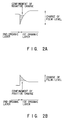
- Fig. 2A is an energy band diagram for explaining confinement of negatively charged carriers on an interface between the first and second organic layers following a change in Fermi level caused by transition of the first organic layer to a metallic state in the organic field effect element according to the present invention;
- Fig. 2B is an energy band diagram for explaining confinement of positively charged carriers on an interface between the first and second organic layers following a change in Fermi level caused by transition of the first organic layer to a metallic state in the organic field effect element according to the present invention;
- Fig. 3 is a sectional view showing an organic field effect element according to Example 1 of the present invention;
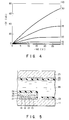
- Fig. 4 is a graph showing a relationship between a potential Vd of a drain electrode with respect to a source electrode and a current Id flowing in the drain electrode using a potential Vg of a gate electrode with respect to the source electrode as a parameter;
- Fig. 5 is a sectional view showing a liquid crystal display using the organic field effect element in Example 1;
- Fig. 6 is a sectional view showing an organic field effect element according to Example 3 of the present invention; and
- Fig. 7 is a graph showing a response of a drain current to an irradiation of the light of a Xe flush lamp having a pulse width of 5 µsec from the gate electrode side of the organic field effect element according to Example 3 of the present invention, under the condition where voltages of -5 V and -50 V are applied to the drain and gate electrodes with respect to the source electrode, respectively.
- In the present invention, any insulating material may be used as a substrate.
- In the present invention, as materials for a first organic layer constituting a channel and a second organic layer formed to be adjacent to the channel, a Π-conjugated polymer, a σ-conjugated polymer, and derivatives thereof are used. Examples of the Π-conjugated polymer are polyparaphenylene, polyacetylene, polypyrrole, polythiophene, polyfuran, polyselenophene, polyaniline, polyazulene, polypyrene, polyfluorene, polyparaphenylenevinylene, polythienylenevinylene, polybenzofuran, polybenzothiophene, polyindole, polyvinylcarbazole, polydibenzofuran, polyisothianaphthene, polyisonaphthothiophene, polydiacethylene, polyphenylenesulfide, and polyphenyleneoxide. Examples of the σ-conjugated polymer are polysilane and polygermane.
- As methods of forming the first and second organic layers, deposition, electrochemical polymerization, photo-irradated electrochemical polymerization, gas-phase polymerization, a method in which a prepolymer is polymerized by heat or a catalyst, and a method in which a polymer is dissolved in a solvent to be coated and dried are used.
- In the present invention, the second organic layer has a carrier concentration different from that of the first organic layer, e.g., the second organic layer has a carrier concentration higher than that of the first organic layer in a dark state or a light irradiation state. The carrier concentration of the second organic layer becomes higher than that of the first organic layer, for example, by doping a dopant. As a method of doping the dopant in the second organic layer, the following methods are used, in which the layer is exposed to a doping vapor in the atmospheric pressure, the layer is exposed to a doping vapor at a reduced pressure, the layer is electrochemically doped in a solution containing a dopant, a dopant is brought into contact with the second organic layer to be thermally diffused, and a dopant is ion-implanted in the layer.
- When electrons are used as carriers, examples of the dopant are halogens (e.g., I₂, Cℓ₂, Br₂, ICℓ, ICℓ₃, IBr, and IF), Lewis acids (e.g., PF₅, AsF₅, SbF₅, BF₃, BCℓ₃, BBr₃, and SO₃), protonic acids, organic acids, or amino acids (e.g., HF, HCℓ, HNO₃, H₂SO₄, HCℓO₄, FSO₃H, CℓSO₃H, and CF₃SO₃H), transition metal compounds (e.g., FeCℓ₃, FeOCℓ, TiCℓ₄, ZrCℓ₄, HfCℓ₄, NbF₅, NbCℓ₅, TaCℓ₅, MoF₅, MoCℓ₅, WF₆, WCℓ₆, UF₆, and LnCℓ₃ (Ln is a lanthanoid)), anions (e.g., Cℓ⁻, Br⁻, I⁻, CℓO₄⁻, BF₄⁻, PF₆⁻, AsF₆⁻, SbF₆⁻, and anions of various sulfonic acids). When holes are used as carriers, examples of the dopant are cations (e.g., H⁺, Li⁺, Na⁺, K⁺, Rb⁺, and Cs⁺), alkali metals (e.g., Li, Na, K, Rb, and Cs), alkaline-earth metals (e.g., Ca, Sr, and Br), O₂, XeOF₄, (NO₂⁺) (SbF₆⁻), (NO₂⁺) (SbCℓ₆⁻), (NO₂⁺) (BF₄⁻), AgCℓO₄, H₂IrCℓ₆, La(NO₃)₃·6H2O, FSO₂OOSO₂F, Eu, acetylcholine, R₄N⁺ (R is an alkyl group), R₄P⁺ (R is an alkyl group), R₆As⁺ (R is an alkyl group), and R₃S⁺ (R is an alkyl group). At this time, the carrier concentration N of the second organic layer preferably satisfies a condition of N > 55,000ε/d², where d and ε represent the thickness and permitivity of the second organic layer, respectively. This is because, when the carrier concentration is too low, a current flowing in a channel may not be easily controlled by the potential of a gate electrode.
- In the present invention, the second organic layer may have a stacked structure. For example, the second organic layer may be formed by a stacked structure consisting of a charge generation layer and a charge transport layer. In this case, when the charge generation layer constituting the second organic layer is irradiated with light, carriers are generated and transport through the charge transport layer, so that the carrier concentration of the second organic layer becomes higher than that of the first organic layer.
- Any material which absorbs light and efficiently generates carriers may be used as a material constituting the charge generation layer. Examples of the materials are inorganic photoconductors (e.g., selenium, a selenium alloy, CdS, CdSe, CdSSe, ZnO, and ZnS), various crystalline metallic phthalocyanine pigments (e.g., titanylphthalocyanine and vanadylphthalocyanine), various crystalline non-metallic phthalocyanine pigments, azo dyes (e.g., a monoazo dye, a bisazo dye, a trisazo dye, and a tetrakisazo dye), penylene pigments (e.g., penylene anhydride and penylene imide), polycyclic quinon pigments (e.g., a perynone pigment, an indigoid dye, a quinacridone pigment, anthraquinone, and dibromoanthoanthrone), aggregate complexes (consisting of a cyanine dye, a xanthene dye, a pyrinium dye, or a thiapyrinium die and a polycarbonate resin, a charge-transfer complex (consisting of an electron-donor material such as an azulenium dye, a squalinium dye, and poly-N-carbazole and an electron-acceptor material such as trinitrofluorenone.
- The charge generation layer may consist of only a charge generating material or may consist of the charge generating material and a binder polymer. As the binder polymer, a polyvinylbutyral resin, a phenoxy resin, or the like is used. As a method of forming the charge generation layer, a coating method (e.g., a spin coating method, an immersion pulling method, a roller coating method, a doctor blade method, and a spray method), a vacuum deposition method, a sputtering method, a plasma CVD method using glow discharge, or the like is used. A proper method is selected from these methods in accordance with the type of a charge generating material to be used.
- As a material constituting the charge transport layer, the above Π-conjugated polymer, σ-conjugated polymer, and derivatives thereof can be used. As a method of forming the charge transport layer consisting of these materials, a deposition method, an electrochemical polymerization, a photo-irradiated electrochemical polymerization, a gas-phase polymerization, a method of polymerizing a prepolymer by heat or a catalyst, a method in which a polymer is dissolved in an appropriate solvent to be coated and dried, or the like is used.
- Another examples of the material constituting the charge transport layer are a hydrazone compound, a pyrazoline compound, an oxadiazole compound, a thiazole compound, a thiadiazole compound, a ketazine compound, an enamine compound, an anisidine compound, a stilbene compound, a butadiene compound, a carbazole compound, and polymer compounds obtained by introducing residual groups thereof to the main or side chains of polymers.
- The charge transport layer consisting of these materials is formed as follows. A binder polymer is dissolved in an appropriate organic solvent, and the above charge transporting material is dissolved or dispersed in the organic solvent to prepare a coating liquid. This coating liquid is coated by a normal coating method and dried. As the coating method, a spin coating method, an immersion pulling method, a roller coating method, a doctor blade method, or a spray coating method is used.
- In this case, examples of the binder polymer are polycarbonate, polyester, polyester carbonate, polyvinyl chloride, an acrylic resin, polyvinyl acetate, a vinyl chloride-vinyl acetate copolymer, polyvinyl acetal, a phenolic resin, a styrene-acrylic copolymer, polyarylate, an alkyd resin, or a phenoxy resin. When the charge transporting material can be formed into a film, a binder polymer is not necessarily required. When the binder polymer is used, a mixing ratio of the charge transporting material to the binder polymer is preferably set to be 1 part by weight : 0.3 to 2 parts by weight.
- In the present invention, as a material for a gate electrode, a material which can form a Schottky junction or a heterojunction with the second organic layer is preferably used. As the material, a metal, a conductive oxide, a semiconductor such as Si treated to decrease its resistance, the above Π-conjugated polymer, the σ-conjugated polymer, or the derivative of the Π-conjugated polymer or the σ-conjugated polymer is used.
- When the second organic layer and the gate electrode do not easily form the above junction, an insulating layer may be formed between the second organic layer and the gate electrode. If the insulating layer is formed when the junction is not easily formed, carriers in the gate electrode are prevented from being injected in the second organic layer. As a result, the second organic layer is depleted, and the carriers can be effectively injected in the first organic layer.
- In the present invention, the material for the source and drain electrodes may be the same or different. As the materials of the source and drain electrodes, materials which can form a Schottky junction or a heterojunction with the second organic layer are preferably used. As the material, similar to the gate electrode, a metal, a conductive oxide, a semiconductor such as Si treated to decrease its resistance, the above Π-conjugated polymer, the σ-conjugated polymer, or the derivative of the Π-conjugated polymer or the σ-conjugated polymer is used. When the source and drain electrodes do not easily form the above junction with the second organic layer, an insulating layer may be formed between the source and drain electrodes and the second organic layer. If the insulating layer is formed when the junction is not easily formed, short circuit between the source and drain electrodes through the second organic layer can be prevented. Note that a space between the source and drain electrodes can be arbitrarily set.
- When an organic field effect element according to the present invention is applied to a liquid crystal display, element structures other than the field effect element are the same as those of the general liquid crystal display.
- Although any insulator can be used as a substrate material, a substrate material on the side through which light passes or on which the light is incident must be transparent within the wavelength region of the light.
- As the materials of a pixel electrode, an address line, a data line, and a counter electrode, a metal, a conductive oxide, a semiconductor such as Si treated to decrease its resistance, the above Π-conjugated polymer, the σ-conjugated polymer, or the derivative of the Π-conjugated polymer or the e-conjugated polymer is used. A part which is in contact with the liquid crystal must consist of an insoluble material in the liquid crystal. In addition, the material for the part on the side through which light passes or on which the light is incident must be transparent within the wavelength region of the light.
- As the liquid crystal, a guest-host liquid crystal, a TN liquid crystal, or a smetic C-phase liquid crystal is used.
- The operative principle of an organic field effect element according to the present invention will be described below.
- When a voltage is not applied to a gate electrode, injection of only a small number of carriers is caused by an electric field on an interface between a second organic layer and a first organic layer constituting a source-drain channel. At this time, if an organic field effect element has a second organic layer having a carrier concentration higher than that of the first organic layer, the channel has a high resistance, and a current flowing in the channel is very small.
- When a voltage is applied to the gate electrode to repel the carriers in the second organic layer from the gate electrode, a large number of carriers are injected in the first organic layer from the second organic layer. For this reason, the resistance of the channel is considerably decreased, and a current flowing in the channel can be increased.
- When a voltage is applied to the gate electrode such that the carriers in the second organic layer are attracted to the gate electrode, a large number of carriers are injected in the second organic layer from the first organic layer. In this case, since the resistance of the channel becomes higher than that obtained when no voltage is applied to the gate electrode, a current flowing in the channel can be decreased.
- The same operative principle as described above is obtained when the second organic layer has a stacked structure consisting of a charge generation layer and a charge transport layer and when light is irradiated on the second organic layer to generate carriers.
- In a Π-conjugated polymer, a σ-conjugated polymer, or derivatives thereof, there are carriers in a state called polaron or bipolaron which is a dimer of the polaron. The polaron has two separated energy bands. When the number of carriers is small, a Fermi level is located at almost the center of the two bands, and the organic layer remains an insulator. When the number of carriers is increased in these energy bands, negative charges and positive charges move in a high-level (close to a vacuum level) polaron band and a low-level polaron band, and the Fermi level shifts into their polaron bands respectively, and the organic layer is changed from an insulating or semiconductor state to a metallic state, thereby considerably decreasing the resistance of the organic layer (e.g., A. J. Heeger et al., Reviews of Modern Physics, Vol. 60, pp. 781-850 (1988); Avadh Saxena et al., Physical Review B, Vol. 35, pp. 3914-3928 (1987); M. A. Abkowitz et al., Philosophical Magazine B, Vol. 61, pp. 25-57 (1990); and Betts et al., Solid State Communications, Vol. 74, pp. 461-464 (1990)). Therefore, when these conjugated polymers are used for the first organic layer, and a sufficient number of carriers are injected from the second organic layer, the first organic layer becomes a metallic state. As shown in Fig. 2A (when carriers are negatively charged) and Fig. 2B (when carriers are positively charged), a change in Fermi level when the state of the first organic layer is changed into the metallic state bends the band of the first organic layer, and carriers are confined in the interface between the first and second organic layers. In this interface, a metallic layer in which carriers are two-dimensionally spread is formed, and a current flowing in the channel is greatly increased.
- As described above, in an organic field effect element according to the present invention, an ON current can be increased to increase an ON/OFF current ratio.
- Examples of the present invention will be described below with reference to the accompanying drawings.
- Fig. 3 is a sectional view showing an organic field effect element in Example 1. A
gate electrode 12 is formed on aglass substrate 11, and a secondorganic layer 13 is formed to cover the entire surface of thegate electrode 12. Asource electrode 14 and adrain electrode 15 are separately formed on the secondorganic layer 13, and a firstorganic layer 16 is formed to constitute a channel between thesource electrode 14 and thedrain electrode 15. - This organic field effect element was manufactured as follows. Polyparaphenylene used for the second organic layer and a prepolymer of polyparaphenylenevinylene used for the first organic layer were synthesized in advance. The polyparaphenylene was synthesized by a method described in Takakazu Yamamoto et al., Chemistry Letters, pp. 1211-1214 (1990) such that paradibromobenzene was condensed in the presence of Mg and Ni complex catalysts. The prepolymer of the polyparaphenylenevinylene was synthesized such that a sulfonium salt obtained by a reaction between dialkylesulfide and paraxylylene dihalide was polymerized using a basic catalyst.
- This prepolymer will be converted into polyparaphenylenevinylene by a thermal polymerizing method described by D. D. C. Bradley, Journal of Physics D: Applied Physics, vol. 20, pp. 1389-1410 (1987).
- An Al layer prospectively serving as the
gate electrode 12 was formed on theglass substrate 11 by vacuum deposition, and then the polyparaphenylene was placed in a tantalum boat and heated at 240°C under 10⁻⁴ Pa to be deposited, thereby forming the secondorganic layer 13 having a thickness of 200 nm on thegate electrode 12. A metal mask was fixed on the secondorganic layer 13, and Ni was vacuum-deposited, thereby forming thesource electrode 14 and thedrain electrode 15. The space between thesource electrode 14 and thedrain electrode 15 was set to be 100 µm. The resultant structure was exposed to an iodine vapor using thesource electrode 14 and thedrain electrode 15 as masks to dope I₂ serving as a dopant in the secondorganic layer 13. As a result, the carrier concentration in the secondorganic layer 13 became 1 x 10¹⁶/cm³. After a solution of the prepolymer of polyparaphenylenevinylene was cast on thesource electrode 14, thedrain electrode 15, and the secondorganic layer 13 by a spinner, the solution was dried in an Ar atmosphere and heated at 300°C under 10-4 Pa to be polymerized, thereby forming the firstorganic layer 16 consisting of a polyparaphenylenevinylene film having a thickness of 2 µm. - In this organic field effect element, a relationship between a potential Vd of the drain electrode with respect to the source electrode and a current Id flowing in the drain electrode is shown in Fig. 4 using a potential Vg of the gate electrode with respect to the source electrode as a parameter. As is apparent from Fig. 4, it is found that the current Id is controlled by the potential Vg. A preferable organic field effect element having a large ON current and a very large ratio of the ON current to an OFF current was obtained.
- Fig. 5 is a sectional view showing a liquid crystal display using an organic field effect element having the same arrangement as that of the organic field effect element in Example 1. A
gate electrode 12 formed on aglass substrate 11 is connected to anaddress line 21. Asource electrode 14 and adrain electrode 15 formed on thegate electrode 12 through a secondorganic layer 13 are connected to a data line 22 and apixel electrode 23 consisting of ITO, respectively. A firstorganic layer 16 is formed on thesource electrode 14 and thedrain electrode 15, and an insulatinglayer 24 consisting of polyimide is formed on the firstorganic layer 16 by deposition to protect the entire surface of the organic field effect element. Acounter electrode 26 consisting of ITO and an insulatinglayer 27 are formed on aglass substrate 25 opposite to theglass substrate 11. The glass substrates 11 and 25 are caused to oppose each other by a normal method to form a liquid crystal cell, and aliquid crystal 28 is sealed between both the substrates. A rubbing process is performed to the insulatinglayers - The response of this liquid crystal display was examined as follows. While potentials of OV and -6 V were kept applied to the data line (source electrode) and the counter electrode, respectively, a potential of -30 V was applied to the address line, and then a potential of 0 V was applied thereto. The liquid crystal was rapidly turned on in response to the potential of -30 V without any delay, and this ON state was kept. On the other hand, while potentials of -12 V and -6 V were kept applied to the data line (source electrode) and the counter electrode, respectively, a potential of -30 V was applied to the address line, and then a potential of 0 V was applied thereto. The liquid crystal was rapidly turned off in response to the potential of -30 V without any delay, and this state was kept.
- In Example 2, carriers are positively charged. In this case, when the potential of the gate electrode (address line) is set to be lower than the potential of either the source electrode (data line) or the drain electrode (pixel electrode), which has a higher potential, the carriers flow from one (the substantial source electrode) of the source and drain electrodes which has a higher potential, to the other (the substantial drain electrode) of the source and drain electrodes, which has a lower potential. The ON and OFF states are controlled by an electric field formed by the charges.
- On the other hand, assume that the carriers are negatively charged. When the potential of the gate electrode (address line) is set to be higher than the potential of either the source electrode (data line) or the drain electrode (pixel electrode), which has a lower potential, the carriers flow from one (the substantial source electrode) of the source and drain electrodes which has a lower potential to the other (the substantial drain electrode) of the source and drain electrodes which has a higher potential. The ON and OFF states are controlled by an electric field formed by the charges.
- When these conditions are satisfied, the potentials of the address line, the data line, and the counter electrode can be arbitrarily set.
- Fig. 6 is a sectional view showing an organic field effect element according to Example 3. A
gate electrode 12 is formed on aglass substrate 11, acharge generation layer 17 is formed to cover the entire surface of thegate electrode 12, and acharge transport layer 18 is formed on thecharge generation layer 17. Thecharge generation layer 17 and thecharge transport layer 18 constitute a secondorganic layer 13. Asource electrode 14 and adrain electrode 15 are separately formed on the secondorganic layer 13, and a firstorganic layer 16 is formed to constitute a channel between the source and drainelectrodes - This organic field effect element was manufactured as follows. A polysilane derivative used for the charge transport layer was synthesized in advance. The polysilane derivative was synthesized in accordance with a method described by J. Devzux et al., European Polymer Journal, Vol. 25, No. 3, pp. 263-266 (1989). That is, Na was mixed in toluene and refluxed, and phenylmethyldichlorosilane serving as a monomer was introduced in the toluene to be polymerized. After the reaction was finished, the Na was treated with ethanol, solid products (polysilane having a phenyl group and a methyl group as substitutent groups) was recovered, washed with deionized water, and dried.
- An Al film which was so thin that the film was transparent was vacuum-deposited on the
glass substrate 11, thereby forming thegate electrode 12. An X-type non-metallic phthalocyanine was dispersed in a trichloroethane solution containing 2 wt% of a phenoxy resin (a weight ratio of the phthalocyanine to the resin is 1 : 1), and the resultant solution was coated by a spinner and dried, thereby forming thecharge generation layer 17 having a thickness of 200 nm. A solution obtained by dissolving the above polysilane derivative in toluene was coated on the charge generation layer and then dried, thereby forming thecharge transport layer 18 having a thickness of 5 µm. A metal mask was fixed on the secondorganic layer 13 consisting of thecharge generation layer 17 and thecharge transport layer 18, and Au was deposited on the resultant structure by electron beam deposition, thereby forming thesource electrode 14 and thedrain electrode 15. The space between thesource electrode 14 and thedrain electrode 15 was set to be 50 µm. - (Bu)₄N⁺CℓO₄⁻ (Bu is a butyl group) serving as an electrolyte and pyrrole serving as a monomer were added to a solution mixture of 99 vol% of well-refined acetonitrile and 1 vol% of distilled water to have concentrations of 0.1 mol% and 0.05 mol%, respectively. The source and drain electrodes and a Pt plate were used as working electrodes and a counter electrode, respectively, and a potential of 3.5 V was applied such that the working electrodes had a positive potential with respect to the counter electrode. In this manner, the above materials were electrochemically polymerized at a constant current having a current density of 0.2 mA/cm² for 10 minutes to stack a polypyrrole layer having a thickness of 200 nm, thereby forming the first
organic layer 16. In this state, however, since the polypyrrole layer was set in a metallic state doped with CℓO₄⁻ ions, the working electrodes were kept at a potential of -2 V for an hour with respect to the counter electrode so as to set a current flowing in the working electrodes at 0 A. The resultant structure was exposed to an ammonia vapor to undope ions. In addition, the resultant structure was left under a vacuum of 10⁻⁴ Pa at 150°C for about 3 hours. - When the organic field effect element is irradiated with light, carriers are generated in the charge generation layer constituting the second organic layer, and the carriers are injected in the charge transport layer constituting the second organic layer. At a time when the carriers are injected in the first organic layer across the charge transport layer, a current begins to flow in the channel. A time interval from when the element is irradiated with light to when the current flows in the channel is determined by the carrier mobility and thickness of the charge transport layer. The magnitude of the current depends on the intensity of the light and the generation efficiency of the carriers of the charge generation layer. There is a merit that these values can be set to be desirable values. In addition, as the characteristic feature of the organic field effect element, for example, serial current signals are generated in response to, parallelly transferred light signals.
- Fig. 7 shows the response of a drain current when the element is irradiated with the light of a Xe flush lamp having a pulse width of 5 µsec from the gate electrode side under the condition where voltages of -5 V and -50 V are applied to the drain and gate electrodes with respect to the source electrode, respectively. As is apparent from Fig. 7, this element is an excellent element having a large ratio of a current (ON current) in an light irradiation state to a current (OFF current) in a non-irradiation state.
- In addition, when the organic field effect element is applied to a liquid crystal display, the ON and OFF states of the liquid crystal display can be controlled by light irradiation.
Claims (19)
- An organic field effect element comprising:
a source electrode (14) and a drain electrode (15) formed separately to each other;
a first organic layer (16) constituting a channel between said source and drain electrodes (14, 15);
a second organic layer (13) formed to be adjacent to said channel and having a carrier concentration different from that of said first organic layer (16); and
a gate electrode (12) formed to be opposite to said channel through said second organic layer (13),
wherein carriers are transferred between said second and first organic layers (13, 16) in response to a voltage applied to said gate electrode (12) to change an electrical conductivity of said channel. - The element according to claim 1, characterized in that the carrier concentration of said second organic layer is higher than that of said first organic layer in one of a dark state and a light irradiated state.
- The element according to claim 1, characterized in that materials of said first organic layer constituting said channel and said second organic layer formed to be adjacent to said channel are selected from the group consisting of a Π-conjugated polymer, a σ-conjugated polymer, and derivatives thereof.
- The element according to claim 3, characterized in that said second organic layer contains a dopant selected from the group consisting of a halogen, a Lewis acid, a protonic acid, an organic acid, amino acid, a transition metal compound, and an anion.
- The element according to claim 3, characterized in that said second organic layer contains a dopant selected from the group consisting of a cation, an alkali metal, an alkaline earth metal, O₂, XeOF₄, (NO₂⁺) (SbF₆⁻), (NO₂⁺) (SbCℓ₆⁻), (NO₂⁺) (BF₄⁻), AgCℓO₄, H₂IrCℓ₆, La(NO₃)₃6H₂O, FSO₂OOSO₂F, Eu, acetylcholine, R₄N⁺ (R is an alkyl group), R₄P⁺ (R is an alkyl group), R₆As⁺ (R is an alkyl group), and R₃S⁺ (R is an alkyl group).
- The element according to claim 1, characterized in that a carrier concentration N in said second organic layer satisfies a condition of N > 55,000 ε/d² where d is a thickness and ε is a permittivity of said second organic layer.
- The element according to claim 3, characterized in that the Π-conjugated polymer is selected from the group consisting of polyparaphenylene, polyacetylene, polypyrrole, polythiophene, polyfuran, polyselenophene, polyaniline, polyazulene, polypyrene, polyfluorene, polyparaphenylenevinylene, polythienylenevinylene, polybenzofuran, polybenzothiophene, polyindole, polyvinylcarbazole, polydibenzofuran, polyisothianaphthene, polyisonaphthothiophene, polydiacethylene, polyphenylenesulfide, and polyphenyleneoxide.
- The element according to claim 3, characterized in that the σ-conjugated polymer is selected from the group consisting of polysilane and polygermane.
- The element according to claim 1, characterized in that said second organic layer has a stacked structure consisting of a charge generation layer and a charge transport layer, and the carrier concentration of said second organic layer is higher than that of said first organic layer when light is irradiated on said charge generation layer.
- The element according to claim 9, characterized in that said charge generation layer contains a material selected from the group consisting of an inorganic photoconductor, metallic phthalocyanine, non-metallic phthalocyanine, an azo dye, a penylene pigment, a polycyclic quinon pigment, an aggregate complex, and a charge transfer complex.
- The element according to claim 9, characterized in that said charge transport layer contains a material selected from the group consisting of a Π-conjugated polymer, a σ-conjugated polymer, and derivatives thereof.
- The element according to claim 9, characterized in that said charge transport layer contains a material selected from the group consisting of a hydrazone compound, a pyrazoline compound, an oxadiazole compound, a thiazole compound, a thiadiazole compound, a ketazine compound, an enamine compound, an anisidine compound, a stilbene compound, a butadiene compound, a carbazole compound, and polymer compounds obtained by introducing residual groups thereof to the main or side chains of polymers.
- The element according to claim 1, characterized in that a material of said gate electrode is selected from materials which can form a Schottky junction or a heterojunction with said second organic layer.
- The element according to claim 13, characterized in that a material of said gate electrode is selected from a metal, a conductive oxide, a semiconductor, a Π-conjugated polymer, a σ-conjugated polymer, and derivatives of the Π-conjugated and the σ-conjugated polymers.
- The element according to claim 1, characterized in that an insulating layer is formed between said second organic layer and said gate electrode.
- The element according to claim 1, characterized in that materials of said source and drain electrodes are selected from materials which can form a Schottky junction or a heterojunction with said second organic layer.
- The element according to claim 16, characterized in that materials of said source and drain electrodes are selected from a metal, a conductive oxide, a semiconductor, a Π-conjugated polymer, a σ-conjugated polymer, and derivatives of the Π-conjugated and the σ-conjugated polymers.
- The element according to claim 1, characterized in that an insulating layer is formed between said second organic layer and said source and drain electrodes.
- The liquid crystal display comprising two substrates arranged to be opposite to each other, a pixel electrode and a drive element formed on an inner surface of one substrate, a counter electrode formed on an inner surface of the other substrate, and a liquid crystal sealed between said substrates,
wherein said drive element includes
a source electrode and a drain electrode formed separately to each other;
a first organic layer constituting a channel between said source and drain electrodes;
a second organic layer formed to be adjacent to said channel and having a carrier concentration different from that of said first organic layer; and
a gate electrode formed to be opposite to said channel through said second organic layer,
such that carriers are transferred between said second and first organic layers in response to a voltage applied to said gate electrode to change an electrical conductivity of said channel.
Applications Claiming Priority (2)
| Application Number | Priority Date | Filing Date | Title |
|---|---|---|---|
| JP20528691A JP3224829B2 (en) | 1991-08-15 | 1991-08-15 | Organic field effect device |
| JP205286/91 | 1991-08-15 |
Publications (2)
| Publication Number | Publication Date |
|---|---|
| EP0528662A1 true EP0528662A1 (en) | 1993-02-24 |
| EP0528662B1 EP0528662B1 (en) | 1995-11-02 |
Family
ID=16504462
Family Applications (1)
| Application Number | Title | Priority Date | Filing Date |
|---|---|---|---|
| EP92307470A Expired - Lifetime EP0528662B1 (en) | 1991-08-15 | 1992-08-14 | Organic field effect transistor |
Country Status (5)
| Country | Link |
|---|---|
| US (1) | US5355235A (en) |
| EP (1) | EP0528662B1 (en) |
| JP (1) | JP3224829B2 (en) |
| KR (1) | KR960015783B1 (en) |
| DE (1) | DE69205766T2 (en) |
Cited By (116)
| Publication number | Priority date | Publication date | Assignee | Title |
|---|---|---|---|---|
| US5659181A (en) * | 1995-03-02 | 1997-08-19 | Lucent Technologies Inc. | Article comprising α-hexathienyl |
| WO1999010939A3 (en) * | 1997-08-22 | 1999-06-10 | Koninkl Philips Electronics Nv | A method of manufacturing a field-effect transistor substantially consisting of organic materials |
| WO2000042668A1 (en) * | 1999-01-15 | 2000-07-20 | The Dow Chemical Company | Semiconducting polymer field effect transistor |
| US6278127B1 (en) * | 1994-12-09 | 2001-08-21 | Agere Systems Guardian Corp. | Article comprising an organic thin film transistor adapted for biasing to form a N-type or a P-type transistor |
| EP1138713A2 (en) * | 2000-03-28 | 2001-10-04 | Sharp Kabushiki Kaisha | Compounds and their manufacture and use |
| WO2001073845A1 (en) * | 2000-03-28 | 2001-10-04 | Koninklijke Philips Electronics N.V. | Integrated circuit with programmable memory element |
| WO2002045183A3 (en) * | 2000-11-30 | 2002-08-01 | Infineon Technologies Ag | Substrate with semiconductor layer, electronic component, electronic circuit, printable composition and method for production thereof |
| WO2003052827A1 (en) * | 2001-12-18 | 2003-06-26 | Matsushita Electric Industrial Co., Ltd. | Non-volatile memory |
| WO2003054970A1 (en) * | 2001-12-11 | 2003-07-03 | Siemens Aktiengesellschaft | Organic field effect transistor with off-set threshold voltage and the use thereof |
| US6603139B1 (en) | 1998-04-16 | 2003-08-05 | Cambridge Display Technology Limited | Polymer devices |
| US6645401B2 (en) | 2001-08-17 | 2003-11-11 | Merck Patent Gmbh | Conjugated copolymers of dithienothiophene with vinylene or acetylene |
| US6676857B2 (en) | 2001-07-25 | 2004-01-13 | Merck Patent Gesellschaft Mit | Mono-, oligo- and poly-4-fluorothiophenes and their use as charge transport materials |
| US6695978B2 (en) | 2001-09-29 | 2004-02-24 | Merck Patent Gesellschaft Mit Beschraenkter Haftung | Mono-, oligo- and polymers of benzo[b]thiophene and 2,2′-bisbenzo[b]thiophene and their use as charge transport materials |
| US6805922B2 (en) | 2001-08-17 | 2004-10-19 | Merck Patent Gmbh | Mono-, oligo-and polyalkylidenefluorenes and their use as charge transport materials |
| US6806374B2 (en) | 2001-07-25 | 2004-10-19 | Merck Patent Gmbh | Mono-, oligo- and poly-3-(1,1-difluoroalkyl)thiophenes and their use as charge transport materials |
| US6824706B2 (en) | 2001-07-25 | 2004-11-30 | Merck Patent Gesellschaft Mit Beschrank Haftung | Mono-, Oligo- and poly-difluorovinyl-(hetero)arylenes, their synthesis and their use as charge transport materials |
| US6863841B2 (en) | 2001-12-13 | 2005-03-08 | Merck Patent Gmbh | Oxadiazole derivative and its use as charge transport and light emitting material |
| US6903958B2 (en) | 2000-09-13 | 2005-06-07 | Siemens Aktiengesellschaft | Method of writing to an organic memory |
| US6913710B2 (en) | 2002-04-24 | 2005-07-05 | Merck Patent Gmbh | Reactive mesogenic benzodithiophenes |
| US7034174B2 (en) | 2001-12-10 | 2006-04-25 | Merck Patent Gmbh | Mono-, oligo- and polymers comprising a 2,6-azulene group and their use as charge transport materials |
| US7095044B2 (en) | 2000-11-28 | 2006-08-22 | Merck Patent Gmbh | Field effect transistors and materials and methods for their manufacture |
| EP1754736A1 (en) | 2005-08-16 | 2007-02-21 | Merck Patent GmbH | Process for the polymerisation of thiophene or selenophene derivatives |
| WO2007068423A1 (en) * | 2005-12-12 | 2007-06-21 | Polyic Gmbh & Co. Kg | Redox systems for stabilization and life extension of polymer semiconductors |
| US7294288B2 (en) | 2003-08-06 | 2007-11-13 | Merck Patent Gesellschaft Mit Beschrankter Haftung | Process of preparing regioregular polymers |
| US7329559B2 (en) | 2003-01-21 | 2008-02-12 | Polyic Gmbh & Co. Kg | Use of conductive carbon black/graphite mixtures for the production of low-cost electronics |
| DE112006002830T5 (en) | 2005-11-24 | 2008-09-25 | Merck Patent Gmbh | Process for the preparation of regioregular polymers |
| DE112006002690T5 (en) | 2005-11-24 | 2008-10-23 | Merck Patent Gmbh | Regioregular polyselenophene |
| CN100451779C (en) * | 2004-09-01 | 2009-01-14 | 财团法人工业技术研究院 | Multiple protective layer method and device for organic thin film transistor |
| US7534034B2 (en) | 2000-12-08 | 2009-05-19 | Polyic Gmbh & Co. Kg | Device for detecting at least one environmental influence |
| CN101174674B (en) * | 2004-09-01 | 2010-07-14 | 财团法人工业技术研究院 | Multiple protection layer of organic thin-film transistor |
| US7786818B2 (en) | 2004-12-10 | 2010-08-31 | Polyic Gmbh & Co. Kg | Electronic component comprising a modulator |
| WO2011018144A2 (en) | 2009-08-12 | 2011-02-17 | Merck Patent Gmbh | Phenanthro[1,10,9,8-c,d,e,f,g]carbazole polymers and their use as organic semiconductors |
| WO2011067192A2 (en) | 2009-12-02 | 2011-06-09 | Basf Se | Dithienobenzo-thieno[3,2-b]thiophene-copolymer and its use as high performance solution processable semiconducting polymer |
| DE112009001505T5 (en) | 2008-08-18 | 2011-07-14 | Merck Patent GmbH, 64293 | Indacenodithiophene and indacenodiselenophene polymers and their use as organic semiconductors |
| DE112009001782T5 (en) | 2008-09-19 | 2011-07-28 | Merck Patent GmbH, 64293 | Bis (thienocyclopenta) benzothiadiazole-derived polymers and their use as organic semiconductors |
| DE112009001784T5 (en) | 2008-09-19 | 2011-07-28 | Merck Patent GmbH, 64293 | Benzo-bis (silo-thiophene) derived polymers and their use as organic semiconductors |
| WO2011098113A2 (en) | 2010-02-15 | 2011-08-18 | Merck Patent Gmbh | Semiconducting polymers |
| WO2011116866A1 (en) | 2010-03-24 | 2011-09-29 | Merck Patent Gmbh | Polymers of 8,9-dihydrobenzo[def]carbazole and their use as organic semiconductors |
| WO2011120951A1 (en) | 2010-03-31 | 2011-10-06 | Basf Se | Annealed dithiophene copolymers |
| WO2011131280A1 (en) | 2010-04-19 | 2011-10-27 | Merck Patent Gmbh | Polymers of benzodithiophene and their use as organic semiconductors |
| WO2012003919A2 (en) | 2010-07-08 | 2012-01-12 | Merck Patent Gmbh | Semiconducting polymers |
| WO2012019683A2 (en) | 2010-08-13 | 2012-02-16 | Merck Patent Gmbh | Anthra[2,3-b:7,6-b']dithiophene derivatives and their use as organic semiconductors |
| WO2012028246A1 (en) | 2010-09-04 | 2012-03-08 | Merck Patent Gmbh | Conjugated polymers |
| WO2012031659A1 (en) | 2010-09-10 | 2012-03-15 | Merck Patent Gmbh | Anthra[2,3-b:7,6b']dithiophene derivatives and their use as organic semiconductors |
| WO2012052099A1 (en) | 2010-10-20 | 2012-04-26 | Merck Patent Gmbh | Conjugated polymers |
| WO2012076092A1 (en) | 2010-12-06 | 2012-06-14 | Merck Patent Gmbh | Non-linear acene derivatives and their use as organic semiconductors |
| WO2012079675A2 (en) | 2010-12-17 | 2012-06-21 | Merck Patent Gmbh | Conjugated polymers |
| WO2012100900A1 (en) | 2011-01-28 | 2012-08-02 | Merck Patent Gmbh | Flavanthrene derivatives and their use as organic semiconductors |
| WO2012123060A1 (en) | 2011-03-11 | 2012-09-20 | Merck Patent Gmbh | Conjugated polymers |
| WO2012123058A1 (en) | 2011-03-11 | 2012-09-20 | Merck Patent Gmbh | Dinaphtho[2,3-a:2',3'-h]phenazines and their use as organic semiconductors |
| WO2012130365A1 (en) | 2011-03-25 | 2012-10-04 | Merck Patent Gmbh | Pyrrolo[3,2-b]pyrrole-2,5-diones and their use as organic semiconductors |
| WO2012143081A1 (en) | 2011-04-18 | 2012-10-26 | Merck Patent Gmbh | Conjugated polymers |
| WO2012156022A1 (en) | 2011-05-16 | 2012-11-22 | Merck Patent Gmbh | Conjugated polymers |
| WO2013000532A1 (en) | 2011-06-28 | 2013-01-03 | Merck Patent Gmbh | Indaceno derivatives as organic semiconductors |
| WO2013007334A2 (en) | 2011-07-08 | 2013-01-17 | Merck Patent Gmbh | Conjugated polymers |
| WO2013010614A2 (en) | 2011-07-19 | 2013-01-24 | Merck Patent Gmbh | Organic semiconductors |
| WO2013010615A1 (en) | 2011-07-21 | 2013-01-24 | Merck Patent Gmbh | Conjugated polymers |
| WO2013013765A1 (en) | 2011-07-27 | 2013-01-31 | Merck Patent Gmbh | Small molecules and their use as organic semiconductors |
| US8367717B2 (en) | 2008-07-02 | 2013-02-05 | Basf Se | High performance solution processable semiconductor based on dithieno [2,3-D:2′, 3′-D′]benzo[1,2-B:4,5-B′] dithiophene |
| WO2013045014A1 (en) | 2011-09-28 | 2013-04-04 | Merck Patent Gmbh | Conjugated polymers |
| WO2013056775A1 (en) | 2011-10-20 | 2013-04-25 | Merck Patent Gmbh | Organic semiconductors |
| DE112011102301T5 (en) | 2010-07-09 | 2013-05-16 | Merck Patent Gmbh | Semiconducting polymers |
| WO2013120591A2 (en) | 2012-02-15 | 2013-08-22 | Merck Patent Gmbh | Conjugated polymers |
| WO2013120575A1 (en) | 2012-02-16 | 2013-08-22 | Merck Patent Gmbh | Organic semiconducting polymers |
| WO2013120590A1 (en) | 2012-02-15 | 2013-08-22 | Merck Patent Gmbh | Conjugated polymers |
| WO2013135339A2 (en) | 2012-03-16 | 2013-09-19 | Merck Patent Gmbh | Conjugated polymers |
| WO2013159862A1 (en) | 2012-04-25 | 2013-10-31 | Merck Patent Gmbh | Conjugated polymers |
| WO2013159863A1 (en) | 2012-04-25 | 2013-10-31 | Merck Patent Gmbh | Conjugated polymers |
| US8598304B2 (en) | 2008-07-02 | 2013-12-03 | Basf Se | Poly(5,5′bis(thiophen-2-yl)-benzo[2,1-b;3,4-b′]dithiophene) and its use as high performance solution processable semiconducting polymer |
| WO2013182262A1 (en) | 2012-06-04 | 2013-12-12 | Merck Patent Gmbh | Organic semiconductors |
| WO2013182264A1 (en) | 2012-06-05 | 2013-12-12 | Merck Patent Gmbh | Small molecules and their use as organic semiconductors |
| WO2014005667A1 (en) | 2012-07-02 | 2014-01-09 | Merck Patent Gmbh | Conjugated polymers |
| WO2014029453A1 (en) | 2012-08-24 | 2014-02-27 | Merck Patent Gmbh | Conjugated polymers |
| WO2014086457A1 (en) | 2012-12-07 | 2014-06-12 | Merck Patent Gmbh | Polymer comprising a naphthalene group and its use in organic electronic devices |
| WO2014094955A1 (en) | 2012-12-18 | 2014-06-26 | Merck Patent Gmbh | Polymer comprising a thiadiazol group, the production of such polymer and its use in organic electronic devices |
| WO2014202184A1 (en) | 2013-06-21 | 2014-12-24 | Merck Patent Gmbh | Conjugated polymers |
| WO2015036075A1 (en) | 2013-09-11 | 2015-03-19 | Merck Patent Gmbh | Cyclohexadiene fullerene derivatives |
| WO2015043722A1 (en) | 2013-09-30 | 2015-04-02 | Merck Patent Gmbh | Azaborinine derivatives, their synthesis and use in organic electronic devices |
| WO2015058827A1 (en) | 2013-10-22 | 2015-04-30 | Merck Patent Gmbh | Conjugated polymers |
| WO2015067336A2 (en) | 2013-11-06 | 2015-05-14 | Merck Patent Gmbh | Conjugated polymers |
| WO2015078551A1 (en) | 2013-11-28 | 2015-06-04 | Merck Patent Gmbh | Novel polycyclic polymer comprising thiophene units, a method of producing and uses of such polymer |
| WO2015139802A1 (en) | 2014-03-17 | 2015-09-24 | Merck Patent Gmbh | Organic semiconducting compounds |
| WO2015149905A1 (en) | 2014-03-31 | 2015-10-08 | Merck Patent Gmbh | Fused bis-aryl fullerene derivatives |
| WO2015192942A1 (en) | 2014-06-17 | 2015-12-23 | Merck Patent Gmbh | Fullerene derivatives |
| WO2016015804A1 (en) | 2014-07-29 | 2016-02-04 | Merck Patent Gmbh | Tetra-heteroaryl indacenodithiophene-based polycyclic polymers and their use |
| EP3070756A1 (en) | 2015-03-18 | 2016-09-21 | Merck Patent GmbH | Semiconductor mixtures comprising nanoparticles |
| WO2016180515A1 (en) | 2015-05-12 | 2016-11-17 | Merck Patent Gmbh | Thiadiazolopyridine polymers, their synthesis and their use |
| WO2017020988A1 (en) | 2015-08-06 | 2017-02-09 | Merck Patent Gmbh | Organic semiconductor compositions and their use in the production of organic electronic devices |
| EP3151297A1 (en) | 2015-09-30 | 2017-04-05 | InnovationLab GmbH | Conjugated polymers with thermally splittable oxalate side groups |
| WO2017157782A1 (en) | 2016-03-15 | 2017-09-21 | Merck Patent Gmbh | Organic semiconductors |
| WO2017157504A1 (en) | 2016-03-15 | 2017-09-21 | Merck Patent Gmbh | Organic semiconductors |
| WO2018007479A1 (en) | 2016-07-08 | 2018-01-11 | Merck Patent Gmbh | Organic semiconducting compounds |
| WO2018007431A1 (en) | 2016-07-08 | 2018-01-11 | Merck Patent Gmbh | Fused dithienothiophene derivatives and their use as organic semiconductors |
| WO2018029159A1 (en) | 2016-08-11 | 2018-02-15 | Merck Patent Gmbh | Organic semiconducting compounds comprising a tetraazapyrene core |
| WO2018036914A1 (en) | 2016-08-22 | 2018-03-01 | Merck Patent Gmbh | Organic semiconducting compounds |
| WO2018041768A1 (en) | 2016-08-29 | 2018-03-08 | Merck Patent Gmbh | 1,3-dithiolo[5,6-f]benzo-2,1,3-thiadiazole or 1,3-dithiolo[6,7-g]quinoxaline based organic semiconductors |
| EP3306690A1 (en) | 2016-10-05 | 2018-04-11 | Merck Patent GmbH | Organic semiconducting compounds |
| WO2018065356A1 (en) | 2016-10-05 | 2018-04-12 | Merck Patent Gmbh | Organic semiconducting compounds |
| WO2018065350A1 (en) | 2016-10-05 | 2018-04-12 | Merck Patent Gmbh | Organic semiconducting compounds |
| WO2018078080A1 (en) | 2016-10-31 | 2018-05-03 | Merck Patent Gmbh | Organic semiconducting compounds |
| EP3333170A1 (en) | 2016-12-06 | 2018-06-13 | Merck Patent GmbH | Asymmetrical polycyclic compounds for use in organic semiconductors |
| WO2018162447A1 (en) | 2017-03-09 | 2018-09-13 | Merck Patent Gmbh | Organic semiconducting compounds |
| WO2019030382A1 (en) | 2017-08-11 | 2019-02-14 | Merck Patent Gmbh | Organic semiconducting polymer |
| WO2019052935A1 (en) | 2017-09-13 | 2019-03-21 | Merck Patent Gmbh | Organic semiconducting compounds |
| WO2019086400A1 (en) | 2017-11-02 | 2019-05-09 | Merck Patent Gmbh | Organic semiconducting compounds |
| WO2019091995A1 (en) | 2017-11-10 | 2019-05-16 | Merck Patent Gmbh | Organic semiconducting compounds |
| WO2019154973A1 (en) | 2018-02-12 | 2019-08-15 | Merck Patent Gmbh | Organic semiconducting compounds |
| WO2019185578A1 (en) | 2018-03-28 | 2019-10-03 | Merck Patent Gmbh | Organic semiconducting compounds |
| WO2019185580A1 (en) | 2018-03-28 | 2019-10-03 | Merck Patent Gmbh | Organic semiconducting compounds |
| WO2019206926A1 (en) | 2018-04-27 | 2019-10-31 | Merck Patent Gmbh | Organic semiconducting polymers |
| WO2020011831A1 (en) | 2018-07-13 | 2020-01-16 | Merck Patent Gmbh | Organic semiconducting compounds |
| WO2020048939A1 (en) | 2018-09-06 | 2020-03-12 | Merck Patent Gmbh | Organic semiconducting compounds |
| WO2020161052A1 (en) | 2019-02-06 | 2020-08-13 | Merck Patent Gmbh | Organic semiconducting polymers |
| WO2020178298A1 (en) | 2019-03-07 | 2020-09-10 | Raynergy Tek Inc. | Organic semiconducting composition |
| WO2020187867A1 (en) | 2019-03-19 | 2020-09-24 | Raynergy Tek Inc. | Organic semiconductors |
| US11930694B2 (en) | 2020-06-08 | 2024-03-12 | University Of Waterloo | Polymer semiconductors containing acrylyl or acrylyl-like side chain and their devices |
Families Citing this family (63)
| Publication number | Priority date | Publication date | Assignee | Title |
|---|---|---|---|---|
| US5597890A (en) * | 1993-11-01 | 1997-01-28 | Research Corporation Technologies, Inc. | Conjugated polymer exciplexes and applications thereof |
| JP3246189B2 (en) * | 1994-06-28 | 2002-01-15 | 株式会社日立製作所 | Semiconductor display device |
| US5574291A (en) * | 1994-12-09 | 1996-11-12 | Lucent Technologies Inc. | Article comprising a thin film transistor with low conductivity organic layer |
| EP1198851B1 (en) * | 1999-07-21 | 2012-03-14 | E Ink Corporation | Reactive formation of dielectric layers and protection of organic layers in organic semiconductor device |
| KR20010089334A (en) * | 1999-08-24 | 2001-10-06 | 요트.게.아. 롤페즈 | Display device |
| WO2002015264A2 (en) | 2000-08-18 | 2002-02-21 | Siemens Aktiengesellschaft | Encapsulated organic-electronic component, method for producing the same and use thereof |
| JP3513097B2 (en) * | 2000-09-29 | 2004-03-31 | 株式会社東芝 | Proton conductive membrane and fuel cell using the same |
| WO2002091494A1 (en) * | 2001-05-07 | 2002-11-14 | Advanced Micro Devices, Inc. | Switch element having memeory effect |
| AU2002340793A1 (en) * | 2001-05-07 | 2002-11-18 | Coatue Corporation | Molecular memory device |
| KR100885276B1 (en) | 2001-05-07 | 2009-02-23 | 어드밴스드 마이크로 디바이시즈, 인코포레이티드 | Floating gate memory device using composite molecular material |
| AU2002340795A1 (en) | 2001-05-07 | 2002-11-18 | Advanced Micro Devices, Inc. | Reversible field-programmable electric interconnects |
| US6873540B2 (en) * | 2001-05-07 | 2005-03-29 | Advanced Micro Devices, Inc. | Molecular memory cell |
| DE60220912T2 (en) * | 2001-05-07 | 2008-02-28 | Advanced Micro Devices, Inc., Sunnyvale | MEMORY DEVICE WITH A SELF-INSTALLING POLYMER AND METHOD FOR THE PRODUCTION THEREOF |
| US6870180B2 (en) * | 2001-06-08 | 2005-03-22 | Lucent Technologies Inc. | Organic polarizable gate transistor apparatus and method |
| US6768157B2 (en) | 2001-08-13 | 2004-07-27 | Advanced Micro Devices, Inc. | Memory device |
| DE60130586T2 (en) | 2001-08-13 | 2008-06-19 | Advanced Micro Devices, Inc., Sunnyvale | CELL |
| US6838720B2 (en) * | 2001-08-13 | 2005-01-04 | Advanced Micro Devices, Inc. | Memory device with active passive layers |
| US6858481B2 (en) | 2001-08-13 | 2005-02-22 | Advanced Micro Devices, Inc. | Memory device with active and passive layers |
| US6806526B2 (en) | 2001-08-13 | 2004-10-19 | Advanced Micro Devices, Inc. | Memory device |
| JP2003177682A (en) * | 2001-09-05 | 2003-06-27 | Konica Corp | Display panel and its manufacturing method |
| KR100433407B1 (en) * | 2002-02-06 | 2004-05-31 | 삼성광주전자 주식회사 | Upright-type vacuum cleaner |
| TWI227806B (en) * | 2002-05-30 | 2005-02-11 | Fujitsu Display Tech | Substrate for liquid crystal display, liquid crystal display having the same, and method of manufacturing the same |
| DE10226370B4 (en) | 2002-06-13 | 2008-12-11 | Polyic Gmbh & Co. Kg | Substrate for an electronic component, use of the substrate, methods for increasing the charge carrier mobility and organic field effect transistor (OFET) |
| JP4878429B2 (en) * | 2002-07-22 | 2012-02-15 | 株式会社リコー | Active element and EL display element having the same |
| EP1525630A2 (en) | 2002-07-29 | 2005-04-27 | Siemens Aktiengesellschaft | Electronic component comprising predominantly organic functional materials and method for the production thereof |
| JP4434563B2 (en) | 2002-09-12 | 2010-03-17 | パイオニア株式会社 | Manufacturing method of organic EL display device |
| US7012276B2 (en) * | 2002-09-17 | 2006-03-14 | Advanced Micro Devices, Inc. | Organic thin film Zener diodes |
| KR100905017B1 (en) * | 2002-12-27 | 2009-06-30 | 엘지디스플레이 주식회사 | Liquid crystal display device and fabrication method thereof |
| JP2004235298A (en) * | 2003-01-29 | 2004-08-19 | Pioneer Electronic Corp | Organic semiconductor element and method for manufacturing the same |
| TW200413803A (en) * | 2003-01-30 | 2004-08-01 | Ind Tech Res Inst | Organic transistor array substrate and its manufacturing method, and LCD including the organic transistor array substrate |
| CN1282260C (en) * | 2003-01-30 | 2006-10-25 | 中国科学院长春应用化学研究所 | Heterojunction-type organic semiconductor field effect transistor containing grid insulating layer and its manufacturing method |
| TWI228189B (en) * | 2003-04-15 | 2005-02-21 | Ind Tech Res Inst | Organic thin film transistor array substrate, its manufacturing method and liquid crystal display including the organic thin film transistor array substrate |
| JP4470398B2 (en) * | 2003-06-23 | 2010-06-02 | Tdk株式会社 | Field effect transistor |
| US7504049B2 (en) * | 2003-08-25 | 2009-03-17 | Semiconductor Energy Laboratory Co., Ltd. | Electrode device for organic device, electronic device having electrode device for organic device, and method of forming electrode device for organic device |
| DE10340644B4 (en) * | 2003-09-03 | 2010-10-07 | Polyic Gmbh & Co. Kg | Mechanical controls for organic polymer electronics |
| DE10340643B4 (en) | 2003-09-03 | 2009-04-16 | Polyic Gmbh & Co. Kg | Printing method for producing a double layer for polymer electronics circuits, and thereby produced electronic component with double layer |
| JP4850389B2 (en) * | 2003-12-12 | 2012-01-11 | 独立行政法人産業技術総合研究所 | Doping method and semiconductor device using the same |
| JP2005223048A (en) * | 2004-02-04 | 2005-08-18 | Ricoh Co Ltd | Semiconductor device, its fabrication process, and display |
| KR101086476B1 (en) * | 2004-04-14 | 2011-11-25 | 엘지디스플레이 주식회사 | Liquid Crystal Display Panel and Method of Fabricating the same |
| JP4449549B2 (en) * | 2004-04-15 | 2010-04-14 | 日本電気株式会社 | ORGANIC THIN FILM TRANSISTOR USING MATERIAL HAVING BRIDGED CYCLIC HYDROCARBON LACTONE STRUCTURE AND MANUFACTURING METHOD |
| DE102004040831A1 (en) | 2004-08-23 | 2006-03-09 | Polyic Gmbh & Co. Kg | Radio-tag compatible outer packaging |
| JP4737964B2 (en) * | 2004-09-30 | 2011-08-03 | 三洋電機株式会社 | Organic semiconductor device |
| US7358571B2 (en) * | 2004-10-20 | 2008-04-15 | Taiwan Semiconductor Manufacturing Company | Isolation spacer for thin SOI devices |
| JP2006154168A (en) * | 2004-11-29 | 2006-06-15 | Seiko Epson Corp | Active matrix substrate, electro-optical device, electronic device and method for manufacturing active matrix substrate |
| DE102004059465A1 (en) | 2004-12-10 | 2006-06-14 | Polyic Gmbh & Co. Kg | recognition system |
| DE102004063435A1 (en) | 2004-12-23 | 2006-07-27 | Polyic Gmbh & Co. Kg | Organic rectifier |
| EP1684365A3 (en) * | 2005-01-20 | 2008-08-13 | Fuji Electric Holdings Co., Ltd. | Transistor |
| DE102005009819A1 (en) | 2005-03-01 | 2006-09-07 | Polyic Gmbh & Co. Kg | electronics assembly |
| DE102005017655B4 (en) | 2005-04-15 | 2008-12-11 | Polyic Gmbh & Co. Kg | Multilayer composite body with electronic function |
| CN100466125C (en) * | 2005-04-18 | 2009-03-04 | 中国科学院长春应用化学研究所 | Electric contacting material and fapparatus of containing organic hetero junction |
| DE102005031448A1 (en) | 2005-07-04 | 2007-01-11 | Polyic Gmbh & Co. Kg | Activatable optical layer |
| JP2007027326A (en) * | 2005-07-14 | 2007-02-01 | Niigata Univ | Organic field-effect transistor |
| DE102005035589A1 (en) | 2005-07-29 | 2007-02-01 | Polyic Gmbh & Co. Kg | Manufacturing electronic component on surface of substrate where component has two overlapping function layers |
| DE102005044306A1 (en) | 2005-09-16 | 2007-03-22 | Polyic Gmbh & Co. Kg | Electronic circuit and method for producing such |
| KR100719566B1 (en) * | 2005-10-22 | 2007-05-17 | 삼성에스디아이 주식회사 | An organic thin film transistor, and a flat panel display therewith |
| US20070145359A1 (en) * | 2005-12-07 | 2007-06-28 | Chi Ming Che | Materials for organic thin film transistors |
| KR101328628B1 (en) * | 2006-07-28 | 2013-11-14 | 삼성디스플레이 주식회사 | Organic Thin Film Transistor Substrate And Fabricating Method Thereof |
| US7785759B2 (en) * | 2008-03-31 | 2010-08-31 | Xerox Corporation | Thiadiazole containing charge transport layer photoconductors |
| US8730416B2 (en) * | 2010-12-17 | 2014-05-20 | Semiconductor Energy Laboratory Co., Ltd. | Liquid crystal display device |
| JP6314831B2 (en) * | 2012-11-13 | 2018-04-25 | 日本電気株式会社 | Negative electrode active material, method for producing the same, and lithium secondary battery |
| US9590176B2 (en) | 2013-03-14 | 2017-03-07 | International Business Machines Corporation | Controlling the conductivity of an oxide by applying voltage pulses to an ionic liquid |
| US10636974B2 (en) | 2014-04-24 | 2020-04-28 | The Trustees Of Columbia University In The City Of New York | Molecular compositions, materials, and methods for efficient multiple exciton generation |
| CN111769142B (en) * | 2020-06-23 | 2022-07-12 | 武汉华星光电半导体显示技术有限公司 | Display panel, preparation method thereof and display device |
Family Cites Families (6)
| Publication number | Priority date | Publication date | Assignee | Title |
|---|---|---|---|---|
| US4873556A (en) * | 1985-05-07 | 1989-10-10 | Mitsubishi Denki Kabushiki Kaisha | Hetero-junction device |
| US5107308A (en) * | 1986-07-04 | 1992-04-21 | Mitsubishi Denki Kabushiki Kaisha | Field-effect transistor |
| JPH01259563A (en) * | 1988-04-08 | 1989-10-17 | Mitsubishi Electric Corp | Field effect transistor |
| EP0418504B1 (en) * | 1989-07-25 | 1995-04-05 | Matsushita Electric Industrial Co., Ltd. | Organic semiconductor memory device having a MISFET structure and its control method |
| US5206525A (en) * | 1989-12-27 | 1993-04-27 | Nippon Petrochemicals Co., Ltd. | Electric element capable of controlling the electric conductivity of π-conjugated macromolecular materials |
| JPH0469971A (en) * | 1990-07-10 | 1992-03-05 | Sumitomo Chem Co Ltd | Field effect transistor |
-
1991
- 1991-08-15 JP JP20528691A patent/JP3224829B2/en not_active Expired - Fee Related
-
1992
- 1992-08-13 US US07/928,704 patent/US5355235A/en not_active Expired - Lifetime
- 1992-08-14 KR KR1019920014617A patent/KR960015783B1/en not_active IP Right Cessation
- 1992-08-14 EP EP92307470A patent/EP0528662B1/en not_active Expired - Lifetime
- 1992-08-14 DE DE69205766T patent/DE69205766T2/en not_active Expired - Fee Related
Non-Patent Citations (1)
| Title |
|---|
| PATENT ABSTRACTS OF JAPAN vol. 14, no. 16 (E-872)12 January 1990 & JP-A-01 259 563 ( MITSUBISHI ELECTRIC CORP. ) 17 October 1989 * |
Cited By (130)
| Publication number | Priority date | Publication date | Assignee | Title |
|---|---|---|---|---|
| US6278127B1 (en) * | 1994-12-09 | 2001-08-21 | Agere Systems Guardian Corp. | Article comprising an organic thin film transistor adapted for biasing to form a N-type or a P-type transistor |
| US5659181A (en) * | 1995-03-02 | 1997-08-19 | Lucent Technologies Inc. | Article comprising α-hexathienyl |
| WO1999010939A3 (en) * | 1997-08-22 | 1999-06-10 | Koninkl Philips Electronics Nv | A method of manufacturing a field-effect transistor substantially consisting of organic materials |
| US6603139B1 (en) | 1998-04-16 | 2003-08-05 | Cambridge Display Technology Limited | Polymer devices |
| US6204515B1 (en) | 1999-01-15 | 2001-03-20 | The Dow Chemical Company | Semiconducting polymer field effect transistor |
| WO2000042668A1 (en) * | 1999-01-15 | 2000-07-20 | The Dow Chemical Company | Semiconducting polymer field effect transistor |
| EP1138713A2 (en) * | 2000-03-28 | 2001-10-04 | Sharp Kabushiki Kaisha | Compounds and their manufacture and use |
| WO2001073845A1 (en) * | 2000-03-28 | 2001-10-04 | Koninklijke Philips Electronics N.V. | Integrated circuit with programmable memory element |
| EP1138713A3 (en) * | 2000-03-28 | 2002-09-04 | Sharp Kabushiki Kaisha | Compounds and their manufacture and use |
| US6903958B2 (en) | 2000-09-13 | 2005-06-07 | Siemens Aktiengesellschaft | Method of writing to an organic memory |
| US7095044B2 (en) | 2000-11-28 | 2006-08-22 | Merck Patent Gmbh | Field effect transistors and materials and methods for their manufacture |
| WO2002045183A3 (en) * | 2000-11-30 | 2002-08-01 | Infineon Technologies Ag | Substrate with semiconductor layer, electronic component, electronic circuit, printable composition and method for production thereof |
| US7432126B2 (en) | 2000-11-30 | 2008-10-07 | Infineon Technologies Ag | Substrate with semiconductor layer, electronic component, electronic circuit, printable composition and method for production thereof |
| US7534034B2 (en) | 2000-12-08 | 2009-05-19 | Polyic Gmbh & Co. Kg | Device for detecting at least one environmental influence |
| US6806374B2 (en) | 2001-07-25 | 2004-10-19 | Merck Patent Gmbh | Mono-, oligo- and poly-3-(1,1-difluoroalkyl)thiophenes and their use as charge transport materials |
| US6824706B2 (en) | 2001-07-25 | 2004-11-30 | Merck Patent Gesellschaft Mit Beschrank Haftung | Mono-, Oligo- and poly-difluorovinyl-(hetero)arylenes, their synthesis and their use as charge transport materials |
| US6676857B2 (en) | 2001-07-25 | 2004-01-13 | Merck Patent Gesellschaft Mit | Mono-, oligo- and poly-4-fluorothiophenes and their use as charge transport materials |
| US6805922B2 (en) | 2001-08-17 | 2004-10-19 | Merck Patent Gmbh | Mono-, oligo-and polyalkylidenefluorenes and their use as charge transport materials |
| US6645401B2 (en) | 2001-08-17 | 2003-11-11 | Merck Patent Gmbh | Conjugated copolymers of dithienothiophene with vinylene or acetylene |
| US6695978B2 (en) | 2001-09-29 | 2004-02-24 | Merck Patent Gesellschaft Mit Beschraenkter Haftung | Mono-, oligo- and polymers of benzo[b]thiophene and 2,2′-bisbenzo[b]thiophene and their use as charge transport materials |
| US7034174B2 (en) | 2001-12-10 | 2006-04-25 | Merck Patent Gmbh | Mono-, oligo- and polymers comprising a 2,6-azulene group and their use as charge transport materials |
| WO2003054970A1 (en) * | 2001-12-11 | 2003-07-03 | Siemens Aktiengesellschaft | Organic field effect transistor with off-set threshold voltage and the use thereof |
| US6863841B2 (en) | 2001-12-13 | 2005-03-08 | Merck Patent Gmbh | Oxadiazole derivative and its use as charge transport and light emitting material |
| WO2003052827A1 (en) * | 2001-12-18 | 2003-06-26 | Matsushita Electric Industrial Co., Ltd. | Non-volatile memory |
| US7027327B2 (en) | 2001-12-18 | 2006-04-11 | Matsushita Electric Industrial Co., Ltd. | Non-volatile memory |
| US6913710B2 (en) | 2002-04-24 | 2005-07-05 | Merck Patent Gmbh | Reactive mesogenic benzodithiophenes |
| US7329559B2 (en) | 2003-01-21 | 2008-02-12 | Polyic Gmbh & Co. Kg | Use of conductive carbon black/graphite mixtures for the production of low-cost electronics |
| US7294288B2 (en) | 2003-08-06 | 2007-11-13 | Merck Patent Gesellschaft Mit Beschrankter Haftung | Process of preparing regioregular polymers |
| CN101174674B (en) * | 2004-09-01 | 2010-07-14 | 财团法人工业技术研究院 | Multiple protection layer of organic thin-film transistor |
| CN100451779C (en) * | 2004-09-01 | 2009-01-14 | 财团法人工业技术研究院 | Multiple protective layer method and device for organic thin film transistor |
| US7786818B2 (en) | 2004-12-10 | 2010-08-31 | Polyic Gmbh & Co. Kg | Electronic component comprising a modulator |
| EP1754736A1 (en) | 2005-08-16 | 2007-02-21 | Merck Patent GmbH | Process for the polymerisation of thiophene or selenophene derivatives |
| DE112006002830T5 (en) | 2005-11-24 | 2008-09-25 | Merck Patent Gmbh | Process for the preparation of regioregular polymers |
| DE112006002690T5 (en) | 2005-11-24 | 2008-10-23 | Merck Patent Gmbh | Regioregular polyselenophene |
| WO2007068423A1 (en) * | 2005-12-12 | 2007-06-21 | Polyic Gmbh & Co. Kg | Redox systems for stabilization and life extension of polymer semiconductors |
| US8367717B2 (en) | 2008-07-02 | 2013-02-05 | Basf Se | High performance solution processable semiconductor based on dithieno [2,3-D:2′, 3′-D′]benzo[1,2-B:4,5-B′] dithiophene |
| US8598304B2 (en) | 2008-07-02 | 2013-12-03 | Basf Se | Poly(5,5′bis(thiophen-2-yl)-benzo[2,1-b;3,4-b′]dithiophene) and its use as high performance solution processable semiconducting polymer |
| DE112009001505T5 (en) | 2008-08-18 | 2011-07-14 | Merck Patent GmbH, 64293 | Indacenodithiophene and indacenodiselenophene polymers and their use as organic semiconductors |
| DE112009001782T5 (en) | 2008-09-19 | 2011-07-28 | Merck Patent GmbH, 64293 | Bis (thienocyclopenta) benzothiadiazole-derived polymers and their use as organic semiconductors |
| DE112009001784T5 (en) | 2008-09-19 | 2011-07-28 | Merck Patent GmbH, 64293 | Benzo-bis (silo-thiophene) derived polymers and their use as organic semiconductors |
| WO2011018144A2 (en) | 2009-08-12 | 2011-02-17 | Merck Patent Gmbh | Phenanthro[1,10,9,8-c,d,e,f,g]carbazole polymers and their use as organic semiconductors |
| WO2011067192A2 (en) | 2009-12-02 | 2011-06-09 | Basf Se | Dithienobenzo-thieno[3,2-b]thiophene-copolymer and its use as high performance solution processable semiconducting polymer |
| US8389670B2 (en) | 2009-12-02 | 2013-03-05 | Basf Se | Dithienobenzo-thieno[3,2-B]thiophene-copolymer and its use as high performance solution processable semiconducting polymer |
| WO2011098113A2 (en) | 2010-02-15 | 2011-08-18 | Merck Patent Gmbh | Semiconducting polymers |
| EP2631230A1 (en) | 2010-02-15 | 2013-08-28 | Merck Patent GmbH | Semiconducting Polymers |
| WO2011116866A1 (en) | 2010-03-24 | 2011-09-29 | Merck Patent Gmbh | Polymers of 8,9-dihydrobenzo[def]carbazole and their use as organic semiconductors |
| WO2011120951A1 (en) | 2010-03-31 | 2011-10-06 | Basf Se | Annealed dithiophene copolymers |
| DE112011101363T5 (en) | 2010-04-19 | 2013-02-07 | Merck Patent Gmbh | Polymers of benzodithiophene and their use as organic semiconductors |
| EP3243818A1 (en) | 2010-04-19 | 2017-11-15 | Merck Patent GmbH | Polymers of benzodithiophene and their use as organic semiconductors |
| WO2011131280A1 (en) | 2010-04-19 | 2011-10-27 | Merck Patent Gmbh | Polymers of benzodithiophene and their use as organic semiconductors |
| WO2012003919A2 (en) | 2010-07-08 | 2012-01-12 | Merck Patent Gmbh | Semiconducting polymers |
| DE112011102301T5 (en) | 2010-07-09 | 2013-05-16 | Merck Patent Gmbh | Semiconducting polymers |
| WO2012019683A2 (en) | 2010-08-13 | 2012-02-16 | Merck Patent Gmbh | Anthra[2,3-b:7,6-b']dithiophene derivatives and their use as organic semiconductors |
| DE112011102915T5 (en) | 2010-09-04 | 2013-07-11 | Merck Patent Gmbh | Conjugated polymers |
| WO2012028246A1 (en) | 2010-09-04 | 2012-03-08 | Merck Patent Gmbh | Conjugated polymers |
| WO2012031659A1 (en) | 2010-09-10 | 2012-03-15 | Merck Patent Gmbh | Anthra[2,3-b:7,6b']dithiophene derivatives and their use as organic semiconductors |
| WO2012052099A1 (en) | 2010-10-20 | 2012-04-26 | Merck Patent Gmbh | Conjugated polymers |
| DE112011103524T5 (en) | 2010-10-20 | 2013-10-17 | Merck Patent Gmbh | Conjugated polymers |
| WO2012076092A1 (en) | 2010-12-06 | 2012-06-14 | Merck Patent Gmbh | Non-linear acene derivatives and their use as organic semiconductors |
| WO2012079675A2 (en) | 2010-12-17 | 2012-06-21 | Merck Patent Gmbh | Conjugated polymers |
| DE112011104436T5 (en) | 2010-12-17 | 2013-09-12 | Merck Patent Gmbh | Conjugated polymers |
| WO2012100900A1 (en) | 2011-01-28 | 2012-08-02 | Merck Patent Gmbh | Flavanthrene derivatives and their use as organic semiconductors |
| WO2012123058A1 (en) | 2011-03-11 | 2012-09-20 | Merck Patent Gmbh | Dinaphtho[2,3-a:2',3'-h]phenazines and their use as organic semiconductors |
| WO2012123060A1 (en) | 2011-03-11 | 2012-09-20 | Merck Patent Gmbh | Conjugated polymers |
| WO2012130365A1 (en) | 2011-03-25 | 2012-10-04 | Merck Patent Gmbh | Pyrrolo[3,2-b]pyrrole-2,5-diones and their use as organic semiconductors |
| WO2012143081A1 (en) | 2011-04-18 | 2012-10-26 | Merck Patent Gmbh | Conjugated polymers |
| WO2012156022A1 (en) | 2011-05-16 | 2012-11-22 | Merck Patent Gmbh | Conjugated polymers |
| WO2013000532A1 (en) | 2011-06-28 | 2013-01-03 | Merck Patent Gmbh | Indaceno derivatives as organic semiconductors |
| WO2013007334A2 (en) | 2011-07-08 | 2013-01-17 | Merck Patent Gmbh | Conjugated polymers |
| WO2013010614A2 (en) | 2011-07-19 | 2013-01-24 | Merck Patent Gmbh | Organic semiconductors |
| WO2013010615A1 (en) | 2011-07-21 | 2013-01-24 | Merck Patent Gmbh | Conjugated polymers |
| WO2013013765A1 (en) | 2011-07-27 | 2013-01-31 | Merck Patent Gmbh | Small molecules and their use as organic semiconductors |
| WO2013045014A1 (en) | 2011-09-28 | 2013-04-04 | Merck Patent Gmbh | Conjugated polymers |
| WO2013056775A1 (en) | 2011-10-20 | 2013-04-25 | Merck Patent Gmbh | Organic semiconductors |
| US9178166B2 (en) | 2012-02-15 | 2015-11-03 | Merck Patent Gmbh | Conjugated polymers |
| WO2013120590A1 (en) | 2012-02-15 | 2013-08-22 | Merck Patent Gmbh | Conjugated polymers |
| WO2013120591A2 (en) | 2012-02-15 | 2013-08-22 | Merck Patent Gmbh | Conjugated polymers |
| WO2013120575A1 (en) | 2012-02-16 | 2013-08-22 | Merck Patent Gmbh | Organic semiconducting polymers |
| WO2013135339A2 (en) | 2012-03-16 | 2013-09-19 | Merck Patent Gmbh | Conjugated polymers |
| WO2013159862A1 (en) | 2012-04-25 | 2013-10-31 | Merck Patent Gmbh | Conjugated polymers |
| WO2013159863A1 (en) | 2012-04-25 | 2013-10-31 | Merck Patent Gmbh | Conjugated polymers |
| WO2013182262A1 (en) | 2012-06-04 | 2013-12-12 | Merck Patent Gmbh | Organic semiconductors |
| WO2013182264A1 (en) | 2012-06-05 | 2013-12-12 | Merck Patent Gmbh | Small molecules and their use as organic semiconductors |
| WO2014005667A1 (en) | 2012-07-02 | 2014-01-09 | Merck Patent Gmbh | Conjugated polymers |
| WO2014029453A1 (en) | 2012-08-24 | 2014-02-27 | Merck Patent Gmbh | Conjugated polymers |
| WO2014086457A1 (en) | 2012-12-07 | 2014-06-12 | Merck Patent Gmbh | Polymer comprising a naphthalene group and its use in organic electronic devices |
| WO2014094955A1 (en) | 2012-12-18 | 2014-06-26 | Merck Patent Gmbh | Polymer comprising a thiadiazol group, the production of such polymer and its use in organic electronic devices |
| WO2014202184A1 (en) | 2013-06-21 | 2014-12-24 | Merck Patent Gmbh | Conjugated polymers |
| WO2015036075A1 (en) | 2013-09-11 | 2015-03-19 | Merck Patent Gmbh | Cyclohexadiene fullerene derivatives |
| WO2015043722A1 (en) | 2013-09-30 | 2015-04-02 | Merck Patent Gmbh | Azaborinine derivatives, their synthesis and use in organic electronic devices |
| WO2015058827A1 (en) | 2013-10-22 | 2015-04-30 | Merck Patent Gmbh | Conjugated polymers |
| WO2015067336A2 (en) | 2013-11-06 | 2015-05-14 | Merck Patent Gmbh | Conjugated polymers |
| WO2015078551A1 (en) | 2013-11-28 | 2015-06-04 | Merck Patent Gmbh | Novel polycyclic polymer comprising thiophene units, a method of producing and uses of such polymer |
| WO2015139802A1 (en) | 2014-03-17 | 2015-09-24 | Merck Patent Gmbh | Organic semiconducting compounds |
| WO2015149905A1 (en) | 2014-03-31 | 2015-10-08 | Merck Patent Gmbh | Fused bis-aryl fullerene derivatives |
| WO2015192942A1 (en) | 2014-06-17 | 2015-12-23 | Merck Patent Gmbh | Fullerene derivatives |
| EP4008708A1 (en) | 2014-06-17 | 2022-06-08 | Nano-C, Inc. | Fullerene derivatives for organic semiconductors |
| WO2016015804A1 (en) | 2014-07-29 | 2016-02-04 | Merck Patent Gmbh | Tetra-heteroaryl indacenodithiophene-based polycyclic polymers and their use |
| EP3070756A1 (en) | 2015-03-18 | 2016-09-21 | Merck Patent GmbH | Semiconductor mixtures comprising nanoparticles |
| WO2016180515A1 (en) | 2015-05-12 | 2016-11-17 | Merck Patent Gmbh | Thiadiazolopyridine polymers, their synthesis and their use |
| WO2017020988A1 (en) | 2015-08-06 | 2017-02-09 | Merck Patent Gmbh | Organic semiconductor compositions and their use in the production of organic electronic devices |
| EP3151297A1 (en) | 2015-09-30 | 2017-04-05 | InnovationLab GmbH | Conjugated polymers with thermally splittable oxalate side groups |
| WO2017157782A1 (en) | 2016-03-15 | 2017-09-21 | Merck Patent Gmbh | Organic semiconductors |
| WO2017157504A1 (en) | 2016-03-15 | 2017-09-21 | Merck Patent Gmbh | Organic semiconductors |
| WO2018007479A1 (en) | 2016-07-08 | 2018-01-11 | Merck Patent Gmbh | Organic semiconducting compounds |
| WO2018007431A1 (en) | 2016-07-08 | 2018-01-11 | Merck Patent Gmbh | Fused dithienothiophene derivatives and their use as organic semiconductors |
| DE112017003977T5 (en) | 2016-08-11 | 2019-07-04 | Merck Patent Gmbh | ORGANIC SEMICONDUCTOR COMPOUNDS COMPRISING A TETRAAZAPYRENE CORE |
| WO2018029159A1 (en) | 2016-08-11 | 2018-02-15 | Merck Patent Gmbh | Organic semiconducting compounds comprising a tetraazapyrene core |
| WO2018036914A1 (en) | 2016-08-22 | 2018-03-01 | Merck Patent Gmbh | Organic semiconducting compounds |
| WO2018041768A1 (en) | 2016-08-29 | 2018-03-08 | Merck Patent Gmbh | 1,3-dithiolo[5,6-f]benzo-2,1,3-thiadiazole or 1,3-dithiolo[6,7-g]quinoxaline based organic semiconductors |
| EP3306690A1 (en) | 2016-10-05 | 2018-04-11 | Merck Patent GmbH | Organic semiconducting compounds |
| WO2018065356A1 (en) | 2016-10-05 | 2018-04-12 | Merck Patent Gmbh | Organic semiconducting compounds |
| WO2018065350A1 (en) | 2016-10-05 | 2018-04-12 | Merck Patent Gmbh | Organic semiconducting compounds |
| WO2018078080A1 (en) | 2016-10-31 | 2018-05-03 | Merck Patent Gmbh | Organic semiconducting compounds |
| EP3333170A1 (en) | 2016-12-06 | 2018-06-13 | Merck Patent GmbH | Asymmetrical polycyclic compounds for use in organic semiconductors |
| WO2018162447A1 (en) | 2017-03-09 | 2018-09-13 | Merck Patent Gmbh | Organic semiconducting compounds |
| WO2019030382A1 (en) | 2017-08-11 | 2019-02-14 | Merck Patent Gmbh | Organic semiconducting polymer |
| WO2019052935A1 (en) | 2017-09-13 | 2019-03-21 | Merck Patent Gmbh | Organic semiconducting compounds |
| WO2019086400A1 (en) | 2017-11-02 | 2019-05-09 | Merck Patent Gmbh | Organic semiconducting compounds |
| WO2019091995A1 (en) | 2017-11-10 | 2019-05-16 | Merck Patent Gmbh | Organic semiconducting compounds |
| WO2019154973A1 (en) | 2018-02-12 | 2019-08-15 | Merck Patent Gmbh | Organic semiconducting compounds |
| WO2019185578A1 (en) | 2018-03-28 | 2019-10-03 | Merck Patent Gmbh | Organic semiconducting compounds |
| WO2019185580A1 (en) | 2018-03-28 | 2019-10-03 | Merck Patent Gmbh | Organic semiconducting compounds |
| WO2019206926A1 (en) | 2018-04-27 | 2019-10-31 | Merck Patent Gmbh | Organic semiconducting polymers |
| WO2020011831A1 (en) | 2018-07-13 | 2020-01-16 | Merck Patent Gmbh | Organic semiconducting compounds |
| WO2020048939A1 (en) | 2018-09-06 | 2020-03-12 | Merck Patent Gmbh | Organic semiconducting compounds |
| WO2020161052A1 (en) | 2019-02-06 | 2020-08-13 | Merck Patent Gmbh | Organic semiconducting polymers |
| WO2020178298A1 (en) | 2019-03-07 | 2020-09-10 | Raynergy Tek Inc. | Organic semiconducting composition |
| WO2020187867A1 (en) | 2019-03-19 | 2020-09-24 | Raynergy Tek Inc. | Organic semiconductors |
| US11930694B2 (en) | 2020-06-08 | 2024-03-12 | University Of Waterloo | Polymer semiconductors containing acrylyl or acrylyl-like side chain and their devices |
Also Published As
| Publication number | Publication date |
|---|---|
| KR960015783B1 (en) | 1996-11-21 |
| US5355235A (en) | 1994-10-11 |
| JPH0548094A (en) | 1993-02-26 |
| DE69205766D1 (en) | 1995-12-07 |
| KR930005247A (en) | 1993-03-23 |
| DE69205766T2 (en) | 1996-04-25 |
| JP3224829B2 (en) | 2001-11-05 |
| EP0528662B1 (en) | 1995-11-02 |
Similar Documents
| Publication | Publication Date | Title |
|---|---|---|
| EP0528662B1 (en) | Organic field effect transistor | |
| US9362505B2 (en) | Fused ring compound and method for producing same, polymer, organic thin film containing those, and organic thin film device and organic thin film transistor comprising such organic thin film | |
| Shallcross et al. | Photochromic transduction layers in organic memory elements | |
| Greiner | Design and synthesis of polymers for light‐emitting diodes | |
| Liu et al. | Electrical conductivity switching and memory effects in poly (N-vinylcarbazole) derivatives with pendant azobenzene chromophores and terminal electron acceptor moieties | |
| Gibson | Control of electrical properties of polymers by chemical modification | |
| US4582587A (en) | Anion-doped polymers of five-membered oxygen family heterocyclic compounds and method for producing same | |
| Morita et al. | Doping effect of buckminsterfullerene in poly (2, 5‐dialkoxy‐p‐phenylene vinylene) | |
| Imae et al. | Synthesis of a novel family of electrochemically-doped vinyl polymers containing pendant oligothiophenes and their electrical and electrochromic properties | |
| Pandey et al. | Photocarrier mobility in regioregular poly (3-hexylthiophene) studied by the time of flight method | |
| Moratti et al. | Light-emitting polymer LEDs | |
| Yoshino et al. | Photoconductivity in C60 doped polyacetylene derivative | |
| Strohriegl et al. | Photoconductive polymers | |
| US7183009B2 (en) | Organic electroluminescent element | |
| EP0594170B1 (en) | An optical information processing element and a light-to-light converting device | |
| Morita et al. | Spectral characteristics of C60-conducting polymer junctions: Various molecular DA type photocells | |
| JP4214706B2 (en) | Optical sensor element, optical sensor device and driving method thereof | |
| KR20080089949A (en) | Dendrimer having triphenylamine core, organic memory device using the same and preparation method thereof | |
| Yoshino et al. | Optical properties of poly (disilanyleneoligothienylene) s and their doping characteristics | |
| Zeng et al. | Synthesis and memory performance of a conjugated polymer with an integrated fluorene, carbazole and oxadiazole backbone | |
| Yoshino et al. | Characteristics of buckminsterfullerene doped conducting polymer | |
| JP3870424B2 (en) | Organic photoconductor and device | |
| Grazulevicius et al. | Charge-transporting polymers and molecular glasses | |
| JP2003500838A (en) | Conductive polymer | |
| Ehrenreich et al. | Advances in research and applications |
Legal Events
| Date | Code | Title | Description |
|---|---|---|---|
| PUAI | Public reference made under article 153(3) epc to a published international application that has entered the european phase |
Free format text: ORIGINAL CODE: 0009012 |
|
| 17P | Request for examination filed |
Effective date: 19920828 |
|
| AK | Designated contracting states |
Kind code of ref document: A1 Designated state(s): DE FR GB |
|
| 17Q | First examination report despatched |
Effective date: 19941205 |
|
| GRAA | (expected) grant |
Free format text: ORIGINAL CODE: 0009210 |
|
| AK | Designated contracting states |
Kind code of ref document: B1 Designated state(s): DE FR GB |
|
| REF | Corresponds to: |
Ref document number: 69205766 Country of ref document: DE Date of ref document: 19951207 |
|
| ET | Fr: translation filed | ||
| PLBE | No opposition filed within time limit |
Free format text: ORIGINAL CODE: 0009261 |
|
| STAA | Information on the status of an ep patent application or granted ep patent |
Free format text: STATUS: NO OPPOSITION FILED WITHIN TIME LIMIT |
|
| 26N | No opposition filed | ||
| REG | Reference to a national code |
Ref country code: GB Ref legal event code: 746 Effective date: 19981023 |
|
| REG | Reference to a national code |
Ref country code: FR Ref legal event code: D6 |
|
| REG | Reference to a national code |
Ref country code: GB Ref legal event code: IF02 |
|
| PGFP | Annual fee paid to national office [announced via postgrant information from national office to epo] |
Ref country code: DE Payment date: 20080829 Year of fee payment: 17 |
|
| PGFP | Annual fee paid to national office [announced via postgrant information from national office to epo] |
Ref country code: FR Payment date: 20080818 Year of fee payment: 17 |
|
| PGFP | Annual fee paid to national office [announced via postgrant information from national office to epo] |
Ref country code: GB Payment date: 20080827 Year of fee payment: 17 |
|
| GBPC | Gb: european patent ceased through non-payment of renewal fee |
Effective date: 20090814 |
|
| REG | Reference to a national code |
Ref country code: FR Ref legal event code: ST Effective date: 20100430 |
|
| PG25 | Lapsed in a contracting state [announced via postgrant information from national office to epo] |
Ref country code: FR Free format text: LAPSE BECAUSE OF NON-PAYMENT OF DUE FEES Effective date: 20090831 Ref country code: DE Free format text: LAPSE BECAUSE OF NON-PAYMENT OF DUE FEES Effective date: 20100302 |
|
| PG25 | Lapsed in a contracting state [announced via postgrant information from national office to epo] |
Ref country code: GB Free format text: LAPSE BECAUSE OF NON-PAYMENT OF DUE FEES Effective date: 20090814 |