EP0530644B1 - Non-Volatile memory cell and fabrication method - Google Patents
Non-Volatile memory cell and fabrication method Download PDFInfo
- Publication number
- EP0530644B1 EP0530644B1 EP92114459A EP92114459A EP0530644B1 EP 0530644 B1 EP0530644 B1 EP 0530644B1 EP 92114459 A EP92114459 A EP 92114459A EP 92114459 A EP92114459 A EP 92114459A EP 0530644 B1 EP0530644 B1 EP 0530644B1
- Authority
- EP
- European Patent Office
- Prior art keywords
- region
- gate
- forming
- source
- gate stack
- Prior art date
- Legal status (The legal status is an assumption and is not a legal conclusion. Google has not performed a legal analysis and makes no representation as to the accuracy of the status listed.)
- Expired - Lifetime
Links
- 238000000034 method Methods 0.000 title claims description 34
- 230000015654 memory Effects 0.000 title claims description 19
- 238000004519 manufacturing process Methods 0.000 title description 6
- 239000000758 substrate Substances 0.000 claims description 19
- 229910052785 arsenic Inorganic materials 0.000 claims description 10
- RQNWIZPPADIBDY-UHFFFAOYSA-N arsenic atom Chemical compound [As] RQNWIZPPADIBDY-UHFFFAOYSA-N 0.000 claims description 10
- 239000012535 impurity Substances 0.000 claims description 8
- 239000004065 semiconductor Substances 0.000 claims description 8
- OAICVXFJPJFONN-UHFFFAOYSA-N Phosphorus Chemical compound [P] OAICVXFJPJFONN-UHFFFAOYSA-N 0.000 claims description 6
- 229910052698 phosphorus Inorganic materials 0.000 claims description 6
- 239000011574 phosphorus Substances 0.000 claims description 6
- 238000000151 deposition Methods 0.000 claims description 5
- 150000004767 nitrides Chemical class 0.000 claims description 5
- 229910021420 polycrystalline silicon Inorganic materials 0.000 claims description 5
- 229920005591 polysilicon Polymers 0.000 claims description 5
- 229910052710 silicon Inorganic materials 0.000 claims description 4
- 239000010703 silicon Substances 0.000 claims description 4
- 239000012212 insulator Substances 0.000 claims 2
- 239000007943 implant Substances 0.000 description 7
- 238000002347 injection Methods 0.000 description 7
- 239000007924 injection Substances 0.000 description 7
- VYPSYNLAJGMNEJ-UHFFFAOYSA-N Silicium dioxide Chemical compound O=[Si]=O VYPSYNLAJGMNEJ-UHFFFAOYSA-N 0.000 description 6
- 230000008901 benefit Effects 0.000 description 6
- 230000008569 process Effects 0.000 description 6
- 230000015572 biosynthetic process Effects 0.000 description 5
- 230000006870 function Effects 0.000 description 5
- 238000009413 insulation Methods 0.000 description 4
- 230000004044 response Effects 0.000 description 4
- 239000000969 carrier Substances 0.000 description 3
- 235000012239 silicon dioxide Nutrition 0.000 description 3
- 239000000377 silicon dioxide Substances 0.000 description 3
- 238000009792 diffusion process Methods 0.000 description 2
- 239000002019 doping agent Substances 0.000 description 2
- 230000007246 mechanism Effects 0.000 description 2
- 230000004048 modification Effects 0.000 description 2
- 238000012986 modification Methods 0.000 description 2
- 230000009471 action Effects 0.000 description 1
- 229910052787 antimony Inorganic materials 0.000 description 1
- WATWJIUSRGPENY-UHFFFAOYSA-N antimony atom Chemical compound [Sb] WATWJIUSRGPENY-UHFFFAOYSA-N 0.000 description 1
- 238000003491 array Methods 0.000 description 1
- 238000007664 blowing Methods 0.000 description 1
- 229910052796 boron Inorganic materials 0.000 description 1
- -1 boron ions Chemical class 0.000 description 1
- 230000015556 catabolic process Effects 0.000 description 1
- 230000000295 complement effect Effects 0.000 description 1
- 239000004020 conductor Substances 0.000 description 1
- 238000010276 construction Methods 0.000 description 1
- 238000006731 degradation reaction Methods 0.000 description 1
- 230000008021 deposition Effects 0.000 description 1
- 238000005137 deposition process Methods 0.000 description 1
- 238000010586 diagram Methods 0.000 description 1
- 230000005684 electric field Effects 0.000 description 1
- 230000002708 enhancing effect Effects 0.000 description 1
- 238000005530 etching Methods 0.000 description 1
- 230000005669 field effect Effects 0.000 description 1
- 239000002784 hot electron Substances 0.000 description 1
- BHEPBYXIRTUNPN-UHFFFAOYSA-N hydridophosphorus(.) (triplet) Chemical compound [PH] BHEPBYXIRTUNPN-UHFFFAOYSA-N 0.000 description 1
- 230000036039 immunity Effects 0.000 description 1
- 238000002513 implantation Methods 0.000 description 1
- 238000011065 in-situ storage Methods 0.000 description 1
- 238000005468 ion implantation Methods 0.000 description 1
- 239000000463 material Substances 0.000 description 1
- 229910044991 metal oxide Inorganic materials 0.000 description 1
- 150000004706 metal oxides Chemical class 0.000 description 1
- 230000001737 promoting effect Effects 0.000 description 1
- 238000009877 rendering Methods 0.000 description 1
- 125000006850 spacer group Chemical group 0.000 description 1
- 230000005641 tunneling Effects 0.000 description 1
Images


Classifications
-
- H—ELECTRICITY
- H01—ELECTRIC ELEMENTS
- H01L—SEMICONDUCTOR DEVICES NOT COVERED BY CLASS H10
- H01L29/00—Semiconductor devices adapted for rectifying, amplifying, oscillating or switching, or capacitors or resistors with at least one potential-jump barrier or surface barrier, e.g. PN junction depletion layer or carrier concentration layer; Details of semiconductor bodies or of electrodes thereof ; Multistep manufacturing processes therefor
- H01L29/66—Types of semiconductor device ; Multistep manufacturing processes therefor
- H01L29/68—Types of semiconductor device ; Multistep manufacturing processes therefor controllable by only the electric current supplied, or only the electric potential applied, to an electrode which does not carry the current to be rectified, amplified or switched
- H01L29/76—Unipolar devices, e.g. field effect transistors
- H01L29/772—Field effect transistors
- H01L29/78—Field effect transistors with field effect produced by an insulated gate
- H01L29/788—Field effect transistors with field effect produced by an insulated gate with floating gate
- H01L29/7881—Programmable transistors with only two possible levels of programmation
- H01L29/7884—Programmable transistors with only two possible levels of programmation charging by hot carrier injection
- H01L29/7886—Hot carrier produced by avalanche breakdown of a PN junction, e.g. FAMOS
-
- H—ELECTRICITY
- H10—SEMICONDUCTOR DEVICES; ELECTRIC SOLID-STATE DEVICES NOT OTHERWISE PROVIDED FOR
- H10B—ELECTRONIC MEMORY DEVICES
- H10B41/00—Electrically erasable-and-programmable ROM [EEPROM] devices comprising floating gates
-
- H—ELECTRICITY
- H10—SEMICONDUCTOR DEVICES; ELECTRIC SOLID-STATE DEVICES NOT OTHERWISE PROVIDED FOR
- H10B—ELECTRONIC MEMORY DEVICES
- H10B69/00—Erasable-and-programmable ROM [EPROM] devices not provided for in groups H10B41/00 - H10B63/00, e.g. ultraviolet erasable-and-programmable ROM [UVEPROM] devices
Definitions
- This invention generally relates to semiconductor memories and more particularly relates to an improved non-volatile memory cell as defined in the precharacterizing part of claim 1 and method of forming the same.
- a read-only memory is a type of memory in which data can be permanently stored, for example, by blowing metallic links during programming thereof. Such type of memory can be conventionally accessed at specific locations to read the programmed contents thereof.
- a much more versatile type of ROM is the electrically programmable read-only memory (EPROM) which can be electrically programmed to store data. Some versions of these devices store data permanently; others, however, can be erased with ultraviolet light or an electrical current.
- an EPROM cell is similar to that of a field effect transistor, but additionally includes a floating gate between the gate conductor and the conduction channel of the transistor.
- a floating gate between the gate conductor and the conduction channel of the transistor.
- Source side injection is a very efficient mechanism for generating hot carriers and a significant gate current.
- a SSI FAMOS Floating gate Avalanche Metal Oxide Semiconductor
- a SSI FAMOS Floating gate Avalanche Metal Oxide Semiconductor cell generally consists of a highly resistive region at the source whose conductivity is not easily modulated by the control gate voltage. Under high gate bias, a high channel electric field region is created at the source, along with a high vertical field there due to high gate-to-source voltage.
- An ideal SSI cell should have the properties of significant gate current at low drain bias and high read current. These properties, however, are not complementary to each other. In other words, enhancing one property will degrade the other one. As such, a cell is presently desired in which each of these properties can be optimized.
- a non-volatile memory cell of the type described above is known from FR-A-2 464 536.
- the non-volatile memory cell described in this document does not have any feature promoting the source side injection mechanism for generating hot carriers and a significant gate current.
- transistor devices comprising lightly doped regions in short channel MOSFETs.
- this type of transistor device it is undesirable to generate hot carriers which may be injected onto a floating gate rather than flow from the source to the drain.
- a non-volatile memory cell structure comprises heavily doped source and drain regions formed in the surface of a semiconductor substrate and separated by a channel region.
- a floating gate is formed over and insulated from the channel region and a control gate is formed over and insulated from the floating gate.
- a lightly doped region is formed in the channel beneath the floating gate and adjoining the source region. The lightly doped region is spaced from the surface of said substrate.
- One advantage of the present invention is that it provides a higher read current than conventional SSI cells when read in the reverse mode, that is when the source is biased high and the drain is grounded.
- Another advantage is that this cell is more resistant to read disturb since the current flow is directed from the surface into the bulk.
- Still another advantage is that the gate injection efficiency is higher since current flow has a component perpendicular to the gate rather than parallel to the gate at the source end.
- Each cell is a floating gate transistor 10 having a source 11, a drain 12, a floating gate 13 and a control gate 14. All of the gates 14 in a row of cells are connected to a row address line 15, and all of the row address lines 15 are connected to a row decoder 16. All of the source and drain electrodes 11 or 12 in a column of cells are connected to a column line 17, and the source and drain column lines 17 are connected at each end to a column decoder 18.
- the column decoder functions to apply either a high voltage (e.g., about 3 to 5 volts) to the drain column line 17 or a low voltage (e.g., ground or V SS , or V BB , depending upon the process) selectively to each source column line 17, in response to a column address on lines 19c and a "0" or "1" data input.
- a high voltage e.g., about 3 to 5 volts
- a low voltage e.g., ground or V SS , or V BB , depending upon the process
- the row decoder 16 functions to apply a high voltage V P or a low voltage V SS or ground to each of the row lines 15 in response to a row address on lines 19r.
- the array may be read using known reading techniques.
- the cell may be erased by applying -11 volts on the gate 14 via row lines 15 while 5 volts is applied on the drain 12 via column lines 17.
- the write takes place at the source and erase takes place at the drain for flash applications.
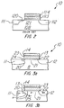
- FIG. 2 a prior art source side injection (SSI) cell is shown.
- An example SSI cell is shown in copending application Serial No. 723,700 corresponding to US-A-5 205 576.
- a highly doped source 111 and drain 112 regions are formed in the surface of a semiconductor substrate 108 and separated from each other by a channel region 121.
- Formed above and electrically insulated from the channel region 121 is a floating gate 113 and formed above and electrically insulated from the floating gate 113 is a control gate 114.
- the SSI cell of FIG. 2 also includes a lightly doped non-overlapped source region 120.
- the width of lightly doped source region 120 is determined by the sidewall spacer (not shown) used during the fabrication process.
- the implant dose of this lightly doped source region 120 determines the trade off between the programming gate current and the read current.
- a non-volatile memory cell 10 sometimes called a Upside Injection cell or USI, comprises a semiconductor substrate 8 which has doped source and drain regions 11 and 12, respectively, formed on the surface.
- the substrate 8 comprises p-type silicon and the source and drain regions 11 and 12 are n+ doped silicon. It is also possible to have a p-channel device with a p-type source and drain formed in a n-type substrate. The source 11 and drain 12 are separated by a channel region 21 which serves as the current path during device operation. Typical source/drain doping concentrations are well known in the current art.
- a conductive floating gate 13 is formed over the channel region 21.
- This floating gate 13 is typically comprised of polysilicon.
- the insulating layer 22 is typically 80 to 120 ⁇ thick for flash EPROMs and 80 to 200 ⁇ thick for UV erasable EPROMs.
- the control gate 14 is separated from the floating gate 13 by an insulation layer 23.
- the insulation layer 23 may be an oxide layer (e.g., silicon dioxide), an oxide/nitride layer, or an oxide/nitride/oxide layer as examples.
- the source region 11 includes a lightly doped portion 20 which is vertically spaced from the upper surface 24 of substrate 8. In essence, the non-overlapped source region 20 is implemented in the vertical direction. As a result, the channel current path will have a vertical component in the source region 11. This feature enhances the amount of programming current since any hot electrons generated in the source region 11 will already have a vertical component without having to go through re-direction collision.
- Figure 3b illustrates an alternative embodiment cell. Illustrated here is an n-channel memory cell which includes a p pocket 25 around the source junction.
- the p pocket 25 may be doped with boron ions with a dose of 10 13 to 10 14 cm -2 at 1000°C for 10 minutes.
- the purpose of the p pocket 25 is to keep most of the voltage drop in the channel region 21 in the region between lightly doped region 20 and floating gate 13.
- all the doping conductivity types would be reversed.
- the optimal source profile was determined to be 3.5 x 10 13 cm -2 at 300 KeV Arsenic for the buried source LDD 20.
- doping concentrations in source LDD 20 range from 10 13 cm -2 to 10 14 cm -2 .
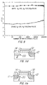
- FIG. 4 illustrates the gate current and the read current as a function of source LDD region 20 energy (in this specific case phosphorus implant energy for a dose of 2 x 10 13 cm -2 except for the highest energy point which is an arsenic implant energy for a dose of 3.5 x 10 13 cm -2 ).
- This figure illustrates the tradeoff between the gate current and the read current.
- FIG. 5a illustrates the characteristics with a drain voltage (V D ) of 5.0V
- FIG. 5b illustrates the characteristics with a drain voltage (V D ) of 3.3V.
- the threshold voltage (V T ) which depends upon the doping concentrations, is plotted as a function of time. Three plots are shown for various gate voltages (V G ).
- FIG. 6 illustrates the wordline stress characteristics of a typical USI cell.
- Wordline stress immunity can be enhanced by minimizing the overlap of the wordline pulse to the bitline pulse during programming.
- the control gate voltage for programming can also be lowered through scaling of the FAMOS channel length. This action further alleviates wordline stress on unprogrammed cells.
- Bitline stress characteristics for these source-side injection cells are shown in FIG. 7. As shown, the characteristics can be improved over conventional cells since the drain profile needs not be designed for hot carrier generation. In fact, for FLASH EPROM applications, the drain junction will be used for electrons tunneling back from the floating gate during erase operation.
- FIG. 8 illustrates read disturb characteristics of a typical USI cell. This figure shows that these cells exhibit more than adequate read-disturb margin for reading from the source.
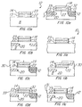
- the gate stack is formed.
- One method of forming an insulation layer for example, is to thermally grow an oxide.
- the surface of substrate 8 may be doped to a given doping concentration prior to forming the insulation layer 22.
- conductive layer 13 is formed over insulating layer 22.
- Conductive layer 13 will become the floating gate.
- forming conductive layer 13 may comprise depositing and doping, or in-situ depositing, polysilicon.
- Layer 23 may comprise multiple layers.
- layer 23 may comprise an oxide layer formed beneath a nitride layer.
- the next process step entails forming a conductive layer 14 for the control gate over insulating layer 23.
- the stacked layers 14, 23, 13 and 22 are patterned and etched to form the desired gate stack. Formation of memories arrays is well known in the art.
- a first implant is performed to create the lightly doped region 20. If the implant is done at high energy, typically about 100 to 200 KeV for phosphorous or 200 to 400 KeV for arsenic as examples, a retrograde source profile is generated. Other dopants such as antimony may be used. If a p-channel cell is built, appropriate p-type dopants will be used.
- a pocket region (not shown) of opposite conductuctivity type of the source and drain (as described with respect to FIG. 3b) is required, this will be formed prior to the implant described above.
- An annealling step can then be included such that the impurities diffuse beneath the gate stack.
- a resist layer 30 is formed over the source side of the device being fabricated. This resist layer 30 will protect the lightly doped region during the drain formation.
- the drain is typically formed by implanting an impurity such as arsenic and/or phosphorus. Diffusion processes may also be used.
- the resist layer 30 is removed after completion of the drain formation.
- Sidewall insulating regions 32 and 33 are formed adjacent to the gate stack and partially over the source and drain regions as illustrated in FIG. 10d.
- the sidewall insulating regions 32 and 33 may typically be a deposited oxide such as silicon dioxide.
- the width of the sidewall oxide is determined by the desired length of the lightly doped region 20.
- the source 11 and drain 12 are created.
- the source/drain formation may be done by diffusion or ion implantation as is well known in the art. If independent doping concentrations are desired for the source 11 and drain 12, the drain 12 may be masked off during the doping process.
- sidewall insulating regions 32 and 33 may be removed to have a structure such as the one shown in FIG. 3.
- FIGs. 11a-11e An alternate fabrication process is shown in FIGs. 11a-11e. Referring first to FIG. 11a, the gate stack is formed as described above with reference to 10a. A resist layer 30 is then formed over one side of the stack region as illustrated in FIG. 11b.
- the lightly doped portion 20 of the source region is then formed as described above with reference to FIG. 10b.
- the resist layer 30 is then removed and a resist layer 31 formed over the source side of the gate stack. This resist layer 31 will prevent doping of the source region during drain formation.
- the drain region 12 is formed by implantation or other doping techniques.
- the source region is not effected by this doping process.
- the sidewall insulating regions 32 and 33 are formed as described above with reference to FIG. 10d.
- the source is then formed as illustrated in FIG. 11e and explained above with reference to FIG. 10e.
- a selective epitaxial deposition process may be utilized to form the buried LDD structure.
Applications Claiming Priority (2)
| Application Number | Priority Date | Filing Date | Title |
|---|---|---|---|
| US07/753,252 US5264384A (en) | 1991-08-30 | 1991-08-30 | Method of making a non-volatile memory cell |
| US753252 | 2010-04-02 |
Publications (3)
| Publication Number | Publication Date |
|---|---|
| EP0530644A2 EP0530644A2 (en) | 1993-03-10 |
| EP0530644A3 EP0530644A3 (en) | 1993-08-04 |
| EP0530644B1 true EP0530644B1 (en) | 1997-10-29 |
Family
ID=25029838
Family Applications (1)
| Application Number | Title | Priority Date | Filing Date |
|---|---|---|---|
| EP92114459A Expired - Lifetime EP0530644B1 (en) | 1991-08-30 | 1992-08-25 | Non-Volatile memory cell and fabrication method |
Country Status (6)
| Country | Link |
|---|---|
| US (3) | US5264384A (un) |
| EP (1) | EP0530644B1 (un) |
| JP (1) | JP3270530B2 (un) |
| KR (1) | KR100293075B1 (un) |
| DE (1) | DE69222913T2 (un) |
| TW (1) | TW249285B (un) |
Cited By (1)
| Publication number | Priority date | Publication date | Assignee | Title |
|---|---|---|---|---|
| TWI792600B (zh) * | 2020-11-16 | 2023-02-11 | 力旺電子股份有限公司 | 記憶體元件 |
Families Citing this family (43)
| Publication number | Priority date | Publication date | Assignee | Title |
|---|---|---|---|---|
| US5424567A (en) * | 1991-05-15 | 1995-06-13 | North American Philips Corporation | Protected programmable transistor with reduced parasitic capacitances and method of fabrication |
| US5264384A (en) * | 1991-08-30 | 1993-11-23 | Texas Instruments Incorporated | Method of making a non-volatile memory cell |
| US6222762B1 (en) | 1992-01-14 | 2001-04-24 | Sandisk Corporation | Multi-state memory |
| US5712180A (en) * | 1992-01-14 | 1998-01-27 | Sundisk Corporation | EEPROM with split gate source side injection |
| US5313421A (en) * | 1992-01-14 | 1994-05-17 | Sundisk Corporation | EEPROM with split gate source side injection |
| US7071060B1 (en) | 1996-02-28 | 2006-07-04 | Sandisk Corporation | EEPROM with split gate source side infection with sidewall spacers |
| EP0552531B1 (en) * | 1992-01-22 | 2000-08-16 | Macronix International Co., Ltd. | Non-volatile memory cell and array architecture |
| US5349225A (en) * | 1993-04-12 | 1994-09-20 | Texas Instruments Incorporated | Field effect transistor with a lightly doped drain |
| EP0655778A3 (en) * | 1993-11-25 | 1996-01-03 | Matsushita Electronics Corp | Method of manufacturing semiconductor memory devices. |
| DE69428516T2 (de) * | 1994-03-28 | 2002-05-08 | St Microelectronics Srl | Flash-EEPROM-Speicher-Matrix und Verfahren zur Vorspannung |
| US5650340A (en) * | 1994-08-18 | 1997-07-22 | Sun Microsystems, Inc. | Method of making asymmetric low power MOS devices |
| KR100192430B1 (ko) * | 1995-08-21 | 1999-06-15 | 구본준 | 비휘발성 메모리 및 이 비휘발성 메모리를 프로그램하는 방법 |
| US5882970A (en) * | 1995-11-03 | 1999-03-16 | United Microelectronics Corporation | Method for fabricating flash memory cell having a decreased overlapped region between its source and gate |
| IT1289540B1 (it) * | 1996-07-10 | 1998-10-15 | Sgs Thomson Microelectronics | Metodo per trasformare automaticamente la fabbricazione di una cella di memoria eprom nella fabbricazione di una cella di memoria |
| KR100238199B1 (ko) * | 1996-07-30 | 2000-01-15 | 윤종용 | 플레쉬 이이피롬(eeprom) 장치 및 그 제조방법 |
| US5900666A (en) * | 1996-12-03 | 1999-05-04 | Advanced Micro Devices, Inc. | Ultra-short transistor fabrication scheme for enhanced reliability |
| US6020232A (en) * | 1996-12-03 | 2000-02-01 | Advanced Micro Devices, Inc. | Process of fabricating transistors having source and drain regions laterally displaced from the transistors gate |
| US5926714A (en) | 1996-12-03 | 1999-07-20 | Advanced Micro Devices, Inc. | Detached drain MOSFET |
| US5898202A (en) * | 1996-12-03 | 1999-04-27 | Advanced Micro Devices, Inc. | Selective spacer formation for optimized silicon area reduction |
| US6060360A (en) * | 1997-04-14 | 2000-05-09 | Taiwan Semiconductor Manufacturing Company | Method of manufacture of P-channel EEprom and flash EEprom devices |
| US6124610A (en) | 1998-06-26 | 2000-09-26 | Advanced Micro Devices, Inc. | Isotropically etching sidewall spacers to be used for both an NMOS source/drain implant and a PMOS LDD implant |
| US6245623B1 (en) * | 1998-11-06 | 2001-06-12 | Advanced Micro Devices, Inc. | CMOS semiconductor device containing N-channel transistor having shallow LDD junctions |
| KR100278661B1 (ko) * | 1998-11-13 | 2001-02-01 | 윤종용 | 비휘발성 메모리소자 및 그 제조방법 |
| JP2002184877A (ja) * | 2000-12-15 | 2002-06-28 | Matsushita Electric Ind Co Ltd | 不揮発性半導体記憶装置及びその製造方法 |
| US7068544B2 (en) * | 2001-08-30 | 2006-06-27 | Micron Technology, Inc. | Flash memory with low tunnel barrier interpoly insulators |
| US7075829B2 (en) * | 2001-08-30 | 2006-07-11 | Micron Technology, Inc. | Programmable memory address and decode circuits with low tunnel barrier interpoly insulators |
| US7135734B2 (en) * | 2001-08-30 | 2006-11-14 | Micron Technology, Inc. | Graded composition metal oxide tunnel barrier interpoly insulators |
| US7132711B2 (en) * | 2001-08-30 | 2006-11-07 | Micron Technology, Inc. | Programmable array logic or memory with p-channel devices and asymmetrical tunnel barriers |
| US7012297B2 (en) * | 2001-08-30 | 2006-03-14 | Micron Technology, Inc. | Scalable flash/NV structures and devices with extended endurance |
| US6784480B2 (en) * | 2002-02-12 | 2004-08-31 | Micron Technology, Inc. | Asymmetric band-gap engineered nonvolatile memory device |
| US7221586B2 (en) | 2002-07-08 | 2007-05-22 | Micron Technology, Inc. | Memory utilizing oxide nanolaminates |
| US6773990B1 (en) * | 2003-05-03 | 2004-08-10 | Advanced Micro Devices, Inc. | Method for reducing short channel effects in memory cells and related structure |
| US7232729B1 (en) * | 2003-05-06 | 2007-06-19 | Spansion Llc | Method for manufacturing a double bitline implant |
| JP4419699B2 (ja) * | 2004-06-16 | 2010-02-24 | ソニー株式会社 | 不揮発性半導体メモリ装置およびその動作方法 |
| US20070099386A1 (en) * | 2005-10-31 | 2007-05-03 | International Business Machines Corporation | Integration scheme for high gain fet in standard cmos process |
| JP4314252B2 (ja) | 2006-07-03 | 2009-08-12 | 株式会社東芝 | 不揮発性半導体記憶装置およびその製造方法 |
| US8320191B2 (en) | 2007-08-30 | 2012-11-27 | Infineon Technologies Ag | Memory cell arrangement, method for controlling a memory cell, memory array and electronic device |
| US7859043B2 (en) * | 2008-02-25 | 2010-12-28 | Tower Semiconductor Ltd. | Three-terminal single poly NMOS non-volatile memory cell |
| US7800156B2 (en) * | 2008-02-25 | 2010-09-21 | Tower Semiconductor Ltd. | Asymmetric single poly NMOS non-volatile memory cell |
| US8344440B2 (en) * | 2008-02-25 | 2013-01-01 | Tower Semiconductor Ltd. | Three-terminal single poly NMOS non-volatile memory cell with shorter program/erase times |
| US9305931B2 (en) | 2011-05-10 | 2016-04-05 | Jonker, Llc | Zero cost NVM cell using high voltage devices in analog process |
| US9230814B2 (en) | 2011-10-28 | 2016-01-05 | Invensas Corporation | Non-volatile memory devices having vertical drain to gate capacitive coupling |
| US8873302B2 (en) * | 2011-10-28 | 2014-10-28 | Invensas Corporation | Common doped region with separate gate control for a logic compatible non-volatile memory cell |
Family Cites Families (27)
| Publication number | Priority date | Publication date | Assignee | Title |
|---|---|---|---|---|
| JPS5189108A (un) * | 1975-01-24 | 1976-08-04 | ||
| JPS5315772A (en) * | 1976-07-28 | 1978-02-14 | Hitachi Ltd | Mis semiconductor device and its production |
| US4163985A (en) * | 1977-09-30 | 1979-08-07 | The United States Of America As Represented By The Secretary Of The Air Force | Nonvolatile punch through memory cell with buried n+ region in channel |
| US4288256A (en) * | 1977-12-23 | 1981-09-08 | International Business Machines Corporation | Method of making FET containing stacked gates |
| JPS54140483A (en) * | 1978-04-21 | 1979-10-31 | Nec Corp | Semiconductor device |
| US4376947A (en) * | 1979-09-04 | 1983-03-15 | Texas Instruments Incorporated | Electrically programmable floating gate semiconductor memory device |
| JPS57102073A (en) * | 1980-12-16 | 1982-06-24 | Mitsubishi Electric Corp | Semiconductor memory and manufacture thereof |
| JPS5950561A (ja) * | 1982-09-17 | 1984-03-23 | Hitachi Ltd | 半導体集積回路装置 |
| JPS59102498A (ja) * | 1982-12-02 | 1984-06-13 | Hitachi Zosen Corp | 湿潤スラツジの焼成装置 |
| JPS60247974A (ja) * | 1984-05-23 | 1985-12-07 | Toshiba Corp | 半導体装置 |
| KR930007195B1 (ko) * | 1984-05-23 | 1993-07-31 | 가부시끼가이샤 히다찌세이사꾸쇼 | 반도체 장치와 그 제조 방법 |
| JPH0760864B2 (ja) * | 1984-07-13 | 1995-06-28 | 株式会社日立製作所 | 半導体集積回路装置 |
| US4698787A (en) * | 1984-11-21 | 1987-10-06 | Exel Microelectronics, Inc. | Single transistor electrically programmable memory device and method |
| EP0197501A3 (en) * | 1985-04-12 | 1986-12-17 | General Electric Company | Extended drain concept for reduced hot electron effect |
| US4680603A (en) * | 1985-04-12 | 1987-07-14 | General Electric Company | Graded extended drain concept for reduced hot electron effect |
| US4804637A (en) * | 1985-09-27 | 1989-02-14 | Texas Instruments Incorporated | EEPROM memory cell and driving circuitry |
| JPS63140582A (ja) * | 1986-12-02 | 1988-06-13 | Toshiba Corp | 半導体装置及びその製造方法 |
| US4835740A (en) * | 1986-12-26 | 1989-05-30 | Kabushiki Kaisha Toshiba | Floating gate type semiconductor memory device |
| US4958321A (en) * | 1988-09-22 | 1990-09-18 | Advanced Micro Devices, Inc. | One transistor flash EPROM cell |
| US5262987A (en) * | 1988-11-17 | 1993-11-16 | Seiko Instruments Inc. | Floating gate semiconductor nonvolatile memory having impurity doped regions for low voltage operation |
| US5216269A (en) * | 1989-03-31 | 1993-06-01 | U.S. Philips Corp. | Electrically-programmable semiconductor memories with buried injector region |
| JPH0783066B2 (ja) * | 1989-08-11 | 1995-09-06 | 株式会社東芝 | 半導体装置の製造方法 |
| JPH0770728B2 (ja) * | 1989-11-15 | 1995-07-31 | 三洋電機株式会社 | 半導体装置の製造方法 |
| JP3111090B2 (ja) * | 1990-08-29 | 2000-11-20 | テキサス インスツルメンツ インコーポレイテツド | 不揮発性メモリセルを作製する方法 |
| US5202576A (en) * | 1990-08-29 | 1993-04-13 | Texas Instruments Incorporated | Asymmetrical non-volatile memory cell, arrays and methods for fabricating same |
| US5424567A (en) * | 1991-05-15 | 1995-06-13 | North American Philips Corporation | Protected programmable transistor with reduced parasitic capacitances and method of fabrication |
| US5264384A (en) * | 1991-08-30 | 1993-11-23 | Texas Instruments Incorporated | Method of making a non-volatile memory cell |
-
1991
- 1991-08-30 US US07/753,252 patent/US5264384A/en not_active Expired - Lifetime
-
1992
- 1992-08-25 EP EP92114459A patent/EP0530644B1/en not_active Expired - Lifetime
- 1992-08-25 DE DE69222913T patent/DE69222913T2/de not_active Expired - Fee Related
- 1992-08-28 JP JP23036092A patent/JP3270530B2/ja not_active Expired - Fee Related
- 1992-08-29 KR KR1019920015635A patent/KR100293075B1/ko not_active IP Right Cessation
-
1993
- 1993-02-18 TW TW082101120A patent/TW249285B/zh not_active IP Right Cessation
- 1993-05-24 US US08/066,816 patent/US5482880A/en not_active Expired - Lifetime
-
1995
- 1995-08-28 US US08/520,350 patent/US5646430A/en not_active Expired - Lifetime
Cited By (1)
| Publication number | Priority date | Publication date | Assignee | Title |
|---|---|---|---|---|
| TWI792600B (zh) * | 2020-11-16 | 2023-02-11 | 力旺電子股份有限公司 | 記憶體元件 |
Also Published As
| Publication number | Publication date |
|---|---|
| US5482880A (en) | 1996-01-09 |
| DE69222913T2 (de) | 1998-05-14 |
| US5264384A (en) | 1993-11-23 |
| JP3270530B2 (ja) | 2002-04-02 |
| US5646430A (en) | 1997-07-08 |
| EP0530644A3 (en) | 1993-08-04 |
| DE69222913D1 (de) | 1997-12-04 |
| JPH06204488A (ja) | 1994-07-22 |
| EP0530644A2 (en) | 1993-03-10 |
| TW249285B (un) | 1995-06-11 |
| KR100293075B1 (ko) | 2001-09-17 |
Similar Documents
| Publication | Publication Date | Title |
|---|---|---|
| EP0530644B1 (en) | Non-Volatile memory cell and fabrication method | |
| US5202576A (en) | Asymmetrical non-volatile memory cell, arrays and methods for fabricating same | |
| US6211011B1 (en) | Method for fabricating asymmetric virtual ground P-channel flash cell | |
| KR920010850B1 (ko) | 소거가능한 프로그래머블 메모리 | |
| US5301150A (en) | Flash erasable single poly EPROM device | |
| EP0495492B1 (en) | Non-volatile memory cell structure and process for forming same | |
| EP0555039B1 (en) | Alternate source virtual ground flash EPROM cell array | |
| EP0360504B1 (en) | One transistor flash eprom cell | |
| US5910925A (en) | EEPROM with split gate source side injection | |
| US5674764A (en) | Method of making asymmetric non-volatile memory cell | |
| US5274588A (en) | Split-gate cell for an EEPROM | |
| US7846794B2 (en) | Low-K spacer structure for flash memory | |
| US20030224564A1 (en) | Non-volatile memory cell having a silicon-oxide nitride-oxide-silicon gate structure and fabrication method of such cell | |
| US6534816B1 (en) | Method and apparatus for injecting charge onto the floating gate of a nonvolatile memory cell | |
| JP5185710B2 (ja) | 電気経路およびメモリセルのフローティングゲートから電荷を消去する方法 | |
| WO2003019573A1 (en) | Non-volatile semiconductor memory and method of operating the same | |
| US5896314A (en) | Asymmetric flash EEPROM with a pocket to focus electron injection and a manufacturing method therefor | |
| US6744105B1 (en) | Memory array having shallow bit line with silicide contact portion and method of formation | |
| US6538925B2 (en) | Semiconductor memory device, method of manufacturing the same and method of driving the same | |
| WO2000045438A1 (en) | Two transistor eeprom cell using p-well for tunneling across a channel | |
| EP0473129B1 (en) | Asymmetrical non-volatile memory cell, arrays and methods for fabricating same | |
| JPH06237000A (ja) | 不揮発性メモリセルおよびその製造方法 | |
| US20060226467A1 (en) | P-channel charge trapping memory device with sub-gate | |
| JP2004158614A (ja) | 不揮発性半導体メモリ装置およびそのデータ書き込み方法 | |
| EP0742956A1 (en) | High density contactless flash eprom array using channel erase |
Legal Events
| Date | Code | Title | Description |
|---|---|---|---|
| PUAI | Public reference made under article 153(3) epc to a published international application that has entered the european phase |
Free format text: ORIGINAL CODE: 0009012 |
|
| AK | Designated contracting states |
Kind code of ref document: A2 Designated state(s): DE FR GB IT NL |
|
| PUAL | Search report despatched |
Free format text: ORIGINAL CODE: 0009013 |
|
| AK | Designated contracting states |
Kind code of ref document: A3 Designated state(s): DE FR GB IT NL |
|
| RIN1 | Information on inventor provided before grant (corrected) |
Inventor name: LIU, DAVID Inventor name: KAYA, CELTIN |
|
| 17P | Request for examination filed |
Effective date: 19940202 |
|
| 17Q | First examination report despatched |
Effective date: 19950110 |
|
| GRAG | Despatch of communication of intention to grant |
Free format text: ORIGINAL CODE: EPIDOS AGRA |
|
| GRAH | Despatch of communication of intention to grant a patent |
Free format text: ORIGINAL CODE: EPIDOS IGRA |
|
| GRAH | Despatch of communication of intention to grant a patent |
Free format text: ORIGINAL CODE: EPIDOS IGRA |
|
| GRAA | (expected) grant |
Free format text: ORIGINAL CODE: 0009210 |
|
| ITF | It: translation for a ep patent filed |
Owner name: BARZANO' E ZANARDO ROMA S.P.A. |
|
| AK | Designated contracting states |
Kind code of ref document: B1 Designated state(s): DE FR GB IT NL |
|
| RIN1 | Information on inventor provided before grant (corrected) |
Inventor name: KAYA, CETIN Inventor name: LIU, DAVID |
|
| REF | Corresponds to: |
Ref document number: 69222913 Country of ref document: DE Date of ref document: 19971204 |
|
| ET | Fr: translation filed | ||
| PLBE | No opposition filed within time limit |
Free format text: ORIGINAL CODE: 0009261 |
|
| STAA | Information on the status of an ep patent application or granted ep patent |
Free format text: STATUS: NO OPPOSITION FILED WITHIN TIME LIMIT |
|
| 26N | No opposition filed | ||
| REG | Reference to a national code |
Ref country code: GB Ref legal event code: IF02 |
|
| PGFP | Annual fee paid to national office [announced via postgrant information from national office to epo] |
Ref country code: GB Payment date: 20060706 Year of fee payment: 15 |
|
| PGFP | Annual fee paid to national office [announced via postgrant information from national office to epo] |
Ref country code: NL Payment date: 20060710 Year of fee payment: 15 |
|
| PGFP | Annual fee paid to national office [announced via postgrant information from national office to epo] |
Ref country code: FR Payment date: 20060803 Year of fee payment: 15 |
|
| PGFP | Annual fee paid to national office [announced via postgrant information from national office to epo] |
Ref country code: IT Payment date: 20060831 Year of fee payment: 15 Ref country code: DE Payment date: 20060831 Year of fee payment: 15 |
|
| GBPC | Gb: european patent ceased through non-payment of renewal fee |
Effective date: 20070825 |
|
| PG25 | Lapsed in a contracting state [announced via postgrant information from national office to epo] |
Ref country code: NL Free format text: LAPSE BECAUSE OF NON-PAYMENT OF DUE FEES Effective date: 20080301 |
|
| NLV4 | Nl: lapsed or anulled due to non-payment of the annual fee |
Effective date: 20080301 |
|
| REG | Reference to a national code |
Ref country code: FR Ref legal event code: ST Effective date: 20080430 |
|
| PG25 | Lapsed in a contracting state [announced via postgrant information from national office to epo] |
Ref country code: DE Free format text: LAPSE BECAUSE OF NON-PAYMENT OF DUE FEES Effective date: 20080301 |
|
| PG25 | Lapsed in a contracting state [announced via postgrant information from national office to epo] |
Ref country code: FR Free format text: LAPSE BECAUSE OF NON-PAYMENT OF DUE FEES Effective date: 20070831 |
|
| PG25 | Lapsed in a contracting state [announced via postgrant information from national office to epo] |
Ref country code: GB Free format text: LAPSE BECAUSE OF NON-PAYMENT OF DUE FEES Effective date: 20070825 |
|
| PG25 | Lapsed in a contracting state [announced via postgrant information from national office to epo] |
Ref country code: IT Free format text: LAPSE BECAUSE OF NON-PAYMENT OF DUE FEES Effective date: 20070825 |