EP0539741A1 - Anodic bonding process with light irradiation - Google Patents
Anodic bonding process with light irradiation Download PDFInfo
- Publication number
- EP0539741A1 EP0539741A1 EP92116628A EP92116628A EP0539741A1 EP 0539741 A1 EP0539741 A1 EP 0539741A1 EP 92116628 A EP92116628 A EP 92116628A EP 92116628 A EP92116628 A EP 92116628A EP 0539741 A1 EP0539741 A1 EP 0539741A1
- Authority
- EP
- European Patent Office
- Prior art keywords
- amorphous
- substrate
- light
- bonding
- glass
- Prior art date
- Legal status (The legal status is an assumption and is not a legal conclusion. Google has not performed a legal analysis and makes no representation as to the accuracy of the status listed.)
- Granted
Links
Images


Classifications
-
- H—ELECTRICITY
- H01—ELECTRIC ELEMENTS
- H01L—SEMICONDUCTOR DEVICES NOT COVERED BY CLASS H10
- H01L24/00—Arrangements for connecting or disconnecting semiconductor or solid-state bodies; Methods or apparatus related thereto
- H01L24/80—Methods for connecting semiconductor or other solid state bodies using means for bonding being attached to, or being formed on, the surface to be connected
- H01L24/83—Methods for connecting semiconductor or other solid state bodies using means for bonding being attached to, or being formed on, the surface to be connected using a layer connector
-
- C—CHEMISTRY; METALLURGY
- C04—CEMENTS; CONCRETE; ARTIFICIAL STONE; CERAMICS; REFRACTORIES
- C04B—LIME, MAGNESIA; SLAG; CEMENTS; COMPOSITIONS THEREOF, e.g. MORTARS, CONCRETE OR LIKE BUILDING MATERIALS; ARTIFICIAL STONE; CERAMICS; REFRACTORIES; TREATMENT OF NATURAL STONE
- C04B37/00—Joining burned ceramic articles with other burned ceramic articles or other articles by heating
- C04B37/04—Joining burned ceramic articles with other burned ceramic articles or other articles by heating with articles made from glass
- C04B37/045—Joining burned ceramic articles with other burned ceramic articles or other articles by heating with articles made from glass characterised by the interlayer used
-
- H—ELECTRICITY
- H01—ELECTRIC ELEMENTS
- H01L—SEMICONDUCTOR DEVICES NOT COVERED BY CLASS H10
- H01L21/00—Processes or apparatus adapted for the manufacture or treatment of semiconductor or solid state devices or of parts thereof
- H01L21/02—Manufacture or treatment of semiconductor devices or of parts thereof
- H01L21/04—Manufacture or treatment of semiconductor devices or of parts thereof the devices having at least one potential-jump barrier or surface barrier, e.g. PN junction, depletion layer or carrier concentration layer
- H01L21/18—Manufacture or treatment of semiconductor devices or of parts thereof the devices having at least one potential-jump barrier or surface barrier, e.g. PN junction, depletion layer or carrier concentration layer the devices having semiconductor bodies comprising elements of Group IV of the Periodic System or AIIIBV compounds with or without impurities, e.g. doping materials
- H01L21/20—Deposition of semiconductor materials on a substrate, e.g. epitaxial growth solid phase epitaxy
- H01L21/2003—Deposition of semiconductor materials on a substrate, e.g. epitaxial growth solid phase epitaxy characterised by the substrate
- H01L21/2007—Bonding of semiconductor wafers to insulating substrates or to semiconducting substrates using an intermediate insulating layer
-
- H—ELECTRICITY
- H01—ELECTRIC ELEMENTS
- H01L—SEMICONDUCTOR DEVICES NOT COVERED BY CLASS H10
- H01L21/00—Processes or apparatus adapted for the manufacture or treatment of semiconductor or solid state devices or of parts thereof
- H01L21/67—Apparatus specially adapted for handling semiconductor or electric solid state devices during manufacture or treatment thereof; Apparatus specially adapted for handling wafers during manufacture or treatment of semiconductor or electric solid state devices or components ; Apparatus not specifically provided for elsewhere
- H01L21/67005—Apparatus not specifically provided for elsewhere
- H01L21/67011—Apparatus for manufacture or treatment
- H01L21/67126—Apparatus for sealing, encapsulating, glassing, decapsulating or the like
-
- H—ELECTRICITY
- H01—ELECTRIC ELEMENTS
- H01L—SEMICONDUCTOR DEVICES NOT COVERED BY CLASS H10
- H01L24/00—Arrangements for connecting or disconnecting semiconductor or solid-state bodies; Methods or apparatus related thereto
- H01L24/74—Apparatus for manufacturing arrangements for connecting or disconnecting semiconductor or solid-state bodies
- H01L24/75—Apparatus for connecting with bump connectors or layer connectors
-
- C—CHEMISTRY; METALLURGY
- C04—CEMENTS; CONCRETE; ARTIFICIAL STONE; CERAMICS; REFRACTORIES
- C04B—LIME, MAGNESIA; SLAG; CEMENTS; COMPOSITIONS THEREOF, e.g. MORTARS, CONCRETE OR LIKE BUILDING MATERIALS; ARTIFICIAL STONE; CERAMICS; REFRACTORIES; TREATMENT OF NATURAL STONE
- C04B2235/00—Aspects relating to ceramic starting mixtures or sintered ceramic products
- C04B2235/65—Aspects relating to heat treatments of ceramic bodies such as green ceramics or pre-sintered ceramics, e.g. burning, sintering or melting processes
- C04B2235/66—Specific sintering techniques, e.g. centrifugal sintering
- C04B2235/665—Local sintering, e.g. laser sintering
-
- C—CHEMISTRY; METALLURGY
- C04—CEMENTS; CONCRETE; ARTIFICIAL STONE; CERAMICS; REFRACTORIES
- C04B—LIME, MAGNESIA; SLAG; CEMENTS; COMPOSITIONS THEREOF, e.g. MORTARS, CONCRETE OR LIKE BUILDING MATERIALS; ARTIFICIAL STONE; CERAMICS; REFRACTORIES; TREATMENT OF NATURAL STONE
- C04B2235/00—Aspects relating to ceramic starting mixtures or sintered ceramic products
- C04B2235/65—Aspects relating to heat treatments of ceramic bodies such as green ceramics or pre-sintered ceramics, e.g. burning, sintering or melting processes
- C04B2235/66—Specific sintering techniques, e.g. centrifugal sintering
- C04B2235/666—Applying a current during sintering, e.g. plasma sintering [SPS], electrical resistance heating or pulse electric current sintering [PECS]
-
- C—CHEMISTRY; METALLURGY
- C04—CEMENTS; CONCRETE; ARTIFICIAL STONE; CERAMICS; REFRACTORIES
- C04B—LIME, MAGNESIA; SLAG; CEMENTS; COMPOSITIONS THEREOF, e.g. MORTARS, CONCRETE OR LIKE BUILDING MATERIALS; ARTIFICIAL STONE; CERAMICS; REFRACTORIES; TREATMENT OF NATURAL STONE
- C04B2237/00—Aspects relating to ceramic laminates or to joining of ceramic articles with other articles by heating
- C04B2237/02—Aspects relating to interlayers, e.g. used to join ceramic articles with other articles by heating
- C04B2237/16—Silicon interlayers
-
- C—CHEMISTRY; METALLURGY
- C04—CEMENTS; CONCRETE; ARTIFICIAL STONE; CERAMICS; REFRACTORIES
- C04B—LIME, MAGNESIA; SLAG; CEMENTS; COMPOSITIONS THEREOF, e.g. MORTARS, CONCRETE OR LIKE BUILDING MATERIALS; ARTIFICIAL STONE; CERAMICS; REFRACTORIES; TREATMENT OF NATURAL STONE
- C04B2237/00—Aspects relating to ceramic laminates or to joining of ceramic articles with other articles by heating
- C04B2237/30—Composition of layers of ceramic laminates or of ceramic or metallic articles to be joined by heating, e.g. Si substrates
- C04B2237/32—Ceramic
-
- H—ELECTRICITY
- H01—ELECTRIC ELEMENTS
- H01L—SEMICONDUCTOR DEVICES NOT COVERED BY CLASS H10
- H01L2224/00—Indexing scheme for arrangements for connecting or disconnecting semiconductor or solid-state bodies and methods related thereto as covered by H01L24/00
- H01L2224/80—Methods for connecting semiconductor or other solid state bodies using means for bonding being attached to, or being formed on, the surface to be connected
- H01L2224/83—Methods for connecting semiconductor or other solid state bodies using means for bonding being attached to, or being formed on, the surface to be connected using a layer connector
- H01L2224/8319—Arrangement of the layer connectors prior to mounting
-
- H—ELECTRICITY
- H01—ELECTRIC ELEMENTS
- H01L—SEMICONDUCTOR DEVICES NOT COVERED BY CLASS H10
- H01L2224/00—Indexing scheme for arrangements for connecting or disconnecting semiconductor or solid-state bodies and methods related thereto as covered by H01L24/00
- H01L2224/80—Methods for connecting semiconductor or other solid state bodies using means for bonding being attached to, or being formed on, the surface to be connected
- H01L2224/83—Methods for connecting semiconductor or other solid state bodies using means for bonding being attached to, or being formed on, the surface to be connected using a layer connector
- H01L2224/832—Applying energy for connecting
- H01L2224/8322—Applying energy for connecting with energy being in the form of electromagnetic radiation
- H01L2224/83224—Applying energy for connecting with energy being in the form of electromagnetic radiation using a laser
-
- H—ELECTRICITY
- H01—ELECTRIC ELEMENTS
- H01L—SEMICONDUCTOR DEVICES NOT COVERED BY CLASS H10
- H01L2224/00—Indexing scheme for arrangements for connecting or disconnecting semiconductor or solid-state bodies and methods related thereto as covered by H01L24/00
- H01L2224/80—Methods for connecting semiconductor or other solid state bodies using means for bonding being attached to, or being formed on, the surface to be connected
- H01L2224/83—Methods for connecting semiconductor or other solid state bodies using means for bonding being attached to, or being formed on, the surface to be connected using a layer connector
- H01L2224/838—Bonding techniques
- H01L2224/83894—Direct bonding, i.e. joining surfaces by means of intermolecular attracting interactions at their interfaces, e.g. covalent bonds, van der Waals forces
-
- H—ELECTRICITY
- H01—ELECTRIC ELEMENTS
- H01L—SEMICONDUCTOR DEVICES NOT COVERED BY CLASS H10
- H01L2924/00—Indexing scheme for arrangements or methods for connecting or disconnecting semiconductor or solid-state bodies as covered by H01L24/00
- H01L2924/01—Chemical elements
- H01L2924/01004—Beryllium [Be]
-
- H—ELECTRICITY
- H01—ELECTRIC ELEMENTS
- H01L—SEMICONDUCTOR DEVICES NOT COVERED BY CLASS H10
- H01L2924/00—Indexing scheme for arrangements or methods for connecting or disconnecting semiconductor or solid-state bodies as covered by H01L24/00
- H01L2924/01—Chemical elements
- H01L2924/01005—Boron [B]
-
- H—ELECTRICITY
- H01—ELECTRIC ELEMENTS
- H01L—SEMICONDUCTOR DEVICES NOT COVERED BY CLASS H10
- H01L2924/00—Indexing scheme for arrangements or methods for connecting or disconnecting semiconductor or solid-state bodies as covered by H01L24/00
- H01L2924/01—Chemical elements
- H01L2924/01006—Carbon [C]
-
- H—ELECTRICITY
- H01—ELECTRIC ELEMENTS
- H01L—SEMICONDUCTOR DEVICES NOT COVERED BY CLASS H10
- H01L2924/00—Indexing scheme for arrangements or methods for connecting or disconnecting semiconductor or solid-state bodies as covered by H01L24/00
- H01L2924/01—Chemical elements
- H01L2924/01011—Sodium [Na]
-
- H—ELECTRICITY
- H01—ELECTRIC ELEMENTS
- H01L—SEMICONDUCTOR DEVICES NOT COVERED BY CLASS H10
- H01L2924/00—Indexing scheme for arrangements or methods for connecting or disconnecting semiconductor or solid-state bodies as covered by H01L24/00
- H01L2924/01—Chemical elements
- H01L2924/01012—Magnesium [Mg]
-
- H—ELECTRICITY
- H01—ELECTRIC ELEMENTS
- H01L—SEMICONDUCTOR DEVICES NOT COVERED BY CLASS H10
- H01L2924/00—Indexing scheme for arrangements or methods for connecting or disconnecting semiconductor or solid-state bodies as covered by H01L24/00
- H01L2924/01—Chemical elements
- H01L2924/01013—Aluminum [Al]
-
- H—ELECTRICITY
- H01—ELECTRIC ELEMENTS
- H01L—SEMICONDUCTOR DEVICES NOT COVERED BY CLASS H10
- H01L2924/00—Indexing scheme for arrangements or methods for connecting or disconnecting semiconductor or solid-state bodies as covered by H01L24/00
- H01L2924/01—Chemical elements
- H01L2924/01019—Potassium [K]
-
- H—ELECTRICITY
- H01—ELECTRIC ELEMENTS
- H01L—SEMICONDUCTOR DEVICES NOT COVERED BY CLASS H10
- H01L2924/00—Indexing scheme for arrangements or methods for connecting or disconnecting semiconductor or solid-state bodies as covered by H01L24/00
- H01L2924/01—Chemical elements
- H01L2924/0102—Calcium [Ca]
-
- H—ELECTRICITY
- H01—ELECTRIC ELEMENTS
- H01L—SEMICONDUCTOR DEVICES NOT COVERED BY CLASS H10
- H01L2924/00—Indexing scheme for arrangements or methods for connecting or disconnecting semiconductor or solid-state bodies as covered by H01L24/00
- H01L2924/01—Chemical elements
- H01L2924/01023—Vanadium [V]
-
- H—ELECTRICITY
- H01—ELECTRIC ELEMENTS
- H01L—SEMICONDUCTOR DEVICES NOT COVERED BY CLASS H10
- H01L2924/00—Indexing scheme for arrangements or methods for connecting or disconnecting semiconductor or solid-state bodies as covered by H01L24/00
- H01L2924/01—Chemical elements
- H01L2924/01024—Chromium [Cr]
-
- H—ELECTRICITY
- H01—ELECTRIC ELEMENTS
- H01L—SEMICONDUCTOR DEVICES NOT COVERED BY CLASS H10
- H01L2924/00—Indexing scheme for arrangements or methods for connecting or disconnecting semiconductor or solid-state bodies as covered by H01L24/00
- H01L2924/01—Chemical elements
- H01L2924/01027—Cobalt [Co]
-
- H—ELECTRICITY
- H01—ELECTRIC ELEMENTS
- H01L—SEMICONDUCTOR DEVICES NOT COVERED BY CLASS H10
- H01L2924/00—Indexing scheme for arrangements or methods for connecting or disconnecting semiconductor or solid-state bodies as covered by H01L24/00
- H01L2924/01—Chemical elements
- H01L2924/0103—Zinc [Zn]
-
- H—ELECTRICITY
- H01—ELECTRIC ELEMENTS
- H01L—SEMICONDUCTOR DEVICES NOT COVERED BY CLASS H10
- H01L2924/00—Indexing scheme for arrangements or methods for connecting or disconnecting semiconductor or solid-state bodies as covered by H01L24/00
- H01L2924/01—Chemical elements
- H01L2924/01032—Germanium [Ge]
-
- H—ELECTRICITY
- H01—ELECTRIC ELEMENTS
- H01L—SEMICONDUCTOR DEVICES NOT COVERED BY CLASS H10
- H01L2924/00—Indexing scheme for arrangements or methods for connecting or disconnecting semiconductor or solid-state bodies as covered by H01L24/00
- H01L2924/01—Chemical elements
- H01L2924/01033—Arsenic [As]
-
- H—ELECTRICITY
- H01—ELECTRIC ELEMENTS
- H01L—SEMICONDUCTOR DEVICES NOT COVERED BY CLASS H10
- H01L2924/00—Indexing scheme for arrangements or methods for connecting or disconnecting semiconductor or solid-state bodies as covered by H01L24/00
- H01L2924/01—Chemical elements
- H01L2924/01037—Rubidium [Rb]
-
- H—ELECTRICITY
- H01—ELECTRIC ELEMENTS
- H01L—SEMICONDUCTOR DEVICES NOT COVERED BY CLASS H10
- H01L2924/00—Indexing scheme for arrangements or methods for connecting or disconnecting semiconductor or solid-state bodies as covered by H01L24/00
- H01L2924/01—Chemical elements
- H01L2924/01038—Strontium [Sr]
-
- H—ELECTRICITY
- H01—ELECTRIC ELEMENTS
- H01L—SEMICONDUCTOR DEVICES NOT COVERED BY CLASS H10
- H01L2924/00—Indexing scheme for arrangements or methods for connecting or disconnecting semiconductor or solid-state bodies as covered by H01L24/00
- H01L2924/01—Chemical elements
- H01L2924/01039—Yttrium [Y]
-
- H—ELECTRICITY
- H01—ELECTRIC ELEMENTS
- H01L—SEMICONDUCTOR DEVICES NOT COVERED BY CLASS H10
- H01L2924/00—Indexing scheme for arrangements or methods for connecting or disconnecting semiconductor or solid-state bodies as covered by H01L24/00
- H01L2924/01—Chemical elements
- H01L2924/01049—Indium [In]
-
- H—ELECTRICITY
- H01—ELECTRIC ELEMENTS
- H01L—SEMICONDUCTOR DEVICES NOT COVERED BY CLASS H10
- H01L2924/00—Indexing scheme for arrangements or methods for connecting or disconnecting semiconductor or solid-state bodies as covered by H01L24/00
- H01L2924/01—Chemical elements
- H01L2924/0105—Tin [Sn]
-
- H—ELECTRICITY
- H01—ELECTRIC ELEMENTS
- H01L—SEMICONDUCTOR DEVICES NOT COVERED BY CLASS H10
- H01L2924/00—Indexing scheme for arrangements or methods for connecting or disconnecting semiconductor or solid-state bodies as covered by H01L24/00
- H01L2924/01—Chemical elements
- H01L2924/01055—Cesium [Cs]
-
- H—ELECTRICITY
- H01—ELECTRIC ELEMENTS
- H01L—SEMICONDUCTOR DEVICES NOT COVERED BY CLASS H10
- H01L2924/00—Indexing scheme for arrangements or methods for connecting or disconnecting semiconductor or solid-state bodies as covered by H01L24/00
- H01L2924/01—Chemical elements
- H01L2924/01056—Barium [Ba]
-
- H—ELECTRICITY
- H01—ELECTRIC ELEMENTS
- H01L—SEMICONDUCTOR DEVICES NOT COVERED BY CLASS H10
- H01L2924/00—Indexing scheme for arrangements or methods for connecting or disconnecting semiconductor or solid-state bodies as covered by H01L24/00
- H01L2924/01—Chemical elements
- H01L2924/01073—Tantalum [Ta]
-
- H—ELECTRICITY
- H01—ELECTRIC ELEMENTS
- H01L—SEMICONDUCTOR DEVICES NOT COVERED BY CLASS H10
- H01L2924/00—Indexing scheme for arrangements or methods for connecting or disconnecting semiconductor or solid-state bodies as covered by H01L24/00
- H01L2924/01—Chemical elements
- H01L2924/01074—Tungsten [W]
-
- H—ELECTRICITY
- H01—ELECTRIC ELEMENTS
- H01L—SEMICONDUCTOR DEVICES NOT COVERED BY CLASS H10
- H01L2924/00—Indexing scheme for arrangements or methods for connecting or disconnecting semiconductor or solid-state bodies as covered by H01L24/00
- H01L2924/01—Chemical elements
- H01L2924/01077—Iridium [Ir]
-
- H—ELECTRICITY
- H01—ELECTRIC ELEMENTS
- H01L—SEMICONDUCTOR DEVICES NOT COVERED BY CLASS H10
- H01L2924/00—Indexing scheme for arrangements or methods for connecting or disconnecting semiconductor or solid-state bodies as covered by H01L24/00
- H01L2924/01—Chemical elements
- H01L2924/01078—Platinum [Pt]
-
- H—ELECTRICITY
- H01—ELECTRIC ELEMENTS
- H01L—SEMICONDUCTOR DEVICES NOT COVERED BY CLASS H10
- H01L2924/00—Indexing scheme for arrangements or methods for connecting or disconnecting semiconductor or solid-state bodies as covered by H01L24/00
- H01L2924/01—Chemical elements
- H01L2924/01079—Gold [Au]
-
- H—ELECTRICITY
- H01—ELECTRIC ELEMENTS
- H01L—SEMICONDUCTOR DEVICES NOT COVERED BY CLASS H10
- H01L2924/00—Indexing scheme for arrangements or methods for connecting or disconnecting semiconductor or solid-state bodies as covered by H01L24/00
- H01L2924/01—Chemical elements
- H01L2924/01082—Lead [Pb]
-
- H—ELECTRICITY
- H01—ELECTRIC ELEMENTS
- H01L—SEMICONDUCTOR DEVICES NOT COVERED BY CLASS H10
- H01L2924/00—Indexing scheme for arrangements or methods for connecting or disconnecting semiconductor or solid-state bodies as covered by H01L24/00
- H01L2924/06—Polymers
- H01L2924/078—Adhesive characteristics other than chemical
- H01L2924/07802—Adhesive characteristics other than chemical not being an ohmic electrical conductor
-
- H—ELECTRICITY
- H01—ELECTRIC ELEMENTS
- H01L—SEMICONDUCTOR DEVICES NOT COVERED BY CLASS H10
- H01L2924/00—Indexing scheme for arrangements or methods for connecting or disconnecting semiconductor or solid-state bodies as covered by H01L24/00
- H01L2924/095—Indexing scheme for arrangements or methods for connecting or disconnecting semiconductor or solid-state bodies as covered by H01L24/00 with a principal constituent of the material being a combination of two or more materials provided in the groups H01L2924/013 - H01L2924/0715
- H01L2924/097—Glass-ceramics, e.g. devitrified glass
- H01L2924/09701—Low temperature co-fired ceramic [LTCC]
-
- H—ELECTRICITY
- H01—ELECTRIC ELEMENTS
- H01L—SEMICONDUCTOR DEVICES NOT COVERED BY CLASS H10
- H01L2924/00—Indexing scheme for arrangements or methods for connecting or disconnecting semiconductor or solid-state bodies as covered by H01L24/00
- H01L2924/10—Details of semiconductor or other solid state devices to be connected
- H01L2924/102—Material of the semiconductor or solid state bodies
- H01L2924/1025—Semiconducting materials
- H01L2924/10251—Elemental semiconductors, i.e. Group IV
- H01L2924/10253—Silicon [Si]
-
- H—ELECTRICITY
- H01—ELECTRIC ELEMENTS
- H01L—SEMICONDUCTOR DEVICES NOT COVERED BY CLASS H10
- H01L2924/00—Indexing scheme for arrangements or methods for connecting or disconnecting semiconductor or solid-state bodies as covered by H01L24/00
- H01L2924/10—Details of semiconductor or other solid state devices to be connected
- H01L2924/102—Material of the semiconductor or solid state bodies
- H01L2924/1025—Semiconducting materials
- H01L2924/1026—Compound semiconductors
- H01L2924/1032—III-V
- H01L2924/10329—Gallium arsenide [GaAs]
-
- H—ELECTRICITY
- H01—ELECTRIC ELEMENTS
- H01L—SEMICONDUCTOR DEVICES NOT COVERED BY CLASS H10
- H01L2924/00—Indexing scheme for arrangements or methods for connecting or disconnecting semiconductor or solid-state bodies as covered by H01L24/00
- H01L2924/10—Details of semiconductor or other solid state devices to be connected
- H01L2924/11—Device type
- H01L2924/12—Passive devices, e.g. 2 terminal devices
- H01L2924/1204—Optical Diode
- H01L2924/12042—LASER
-
- H—ELECTRICITY
- H01—ELECTRIC ELEMENTS
- H01L—SEMICONDUCTOR DEVICES NOT COVERED BY CLASS H10
- H01L2924/00—Indexing scheme for arrangements or methods for connecting or disconnecting semiconductor or solid-state bodies as covered by H01L24/00
- H01L2924/30—Technical effects
- H01L2924/301—Electrical effects
- H01L2924/3025—Electromagnetic shielding
Definitions
- the present invention relates to an anodic bonding process for connecting together a glass and an electric conductor by applying a voltage therebetween, and an apparatus therefor.
- the anodic bonding between a glass and a silicon Si has been carried out by applying a voltage of about 300 V between the glass and Si, with Si as anode, while maintaining the temperature at about 400°C near a transition point of glass, as described by George Wallis and Daniel I. Pomerantz et al. in Journal of Applied Physics, vol. 40, no. 10, September 1969: Received 2 January 1969.
- the bonding between the glass and Si is performed near a transition point of glass, so that thermal strain may possibly occur due to a difference between their thermal expansion coefficients when the temperature drops down to room temperature after the bonding at high temperature, resulting in a risk of peeling off. Therefore, it is required that the thermal expansion coefficients of glass and Si be equal in a wide range from room temperature to connexion temperature.
- a first object of the present invention is to provide an anodic bonding process which can resolve the above-mentioned drawback and allows the secure connection without elevating the temperature to a transition point of glass.
- Fig. 1 is a constitutional view of an apparatus common to first and second embodiments.
- Fig. 2 is a constitutional view of an apparatus in third embodiment.
- Fig. 3 is a cross-sectional view of the bonding between an Si substrate and a photosensitive glass in fourth embodiment of the present invention.
- Fig. 4 is a cross-sectional view of the selective bonding between an Si substrate and a photosensitive glass in fifth embodiment of the present invention.
- Fig. 5 is a cross-sectional view of the selective bonding between an Si substrate and a photosensitive glass in sixth embodiment of the present invention.
- Fig. 6 is a cross-sectional view of the selective bonding between an Si substrate and a photosensitive glass in seventh embodiment of the present invention.
- Fig. 7 is a schematic view of the anodic bonding with light irradiation in eighth embodiment of the present invention.
- Fig. 8 is a view as looked from a direction of arrow A in Fig. 7.
- Fig. 9 is a schematic view of a laser optical system with mask allowing the use of the anodic bonding with light irradiation according to the present invention.
- Fig. 10 is a schematic view of a bonding apparatus allowing the use of the anodic bonding with light irradiation according to the present invention.
- Fig. 11 is an explanation view of a light sensor chip capable of being produced by using the anodic bonding with light irradiation according to the present invention.
- Fig. 12 is an explanation view from the top of a light sensor chip of Fig. 11.
- Fig. 13 is an explanation view of a light memory chip capable of being produced by using the anodic bonding with light irradiation according to the present invention.
- Fig. 14 is an explanation view from the top of a light sensor chip of Fig. 13.
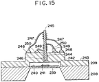
- Fig. 15 is an explanation view of a pressure sensor capable of being produced by using the anodic bonding with light irradiation according to the present invention.
- the anodic bonding process in the preferred embodiments for anodic bonding made between a glass and an electric conductor is characterized by applying a voltage between the glass and the electric conductor, while irradiating a light beam from the glass side or electric conductor side.
- the anodic bonding process using light irradiation with the above-mentioned constitution can be carried out by applying a voltage between the electric conductor and the glass, while a light beam is irradiated so as to relax a network structure of glass and to promote the diffusion of modifier ions in the glass, whereby the network structure of glass is relaxed at relatively low temperatures and modifier ions diffuse to cathode side to cause a great electrostatic attractive force between the electric conductor and the glass, so that the solid phase bonding is achieved.
- the network structure is relaxed by cutting weak binding portions in the network structure of glass or exciting it with oscillation, or modifier ions in the glass are diffused by giving an energy exceeding an activation energy for the diffusion of modifier ions.
- voltage is applied between cathode of glass substrate and anode of Si substrate to generate an electric field.
- modifier ions are attracted to the cathode side and oxygen ions are attracted to the anode side, so that a depletion layer is produced near a bonding interface on the glass side, whereby a great electrostatic attractive force is generated between the glass substrate and the Si substrate.
- the gap between both substrates becomes atomic order due to this electrostatic attractive force, so that the solid phase bonding is possible.
- the network structure of glass is constructed of ionic bonds in various bond distances, there are some portions where relaxation occurs with relatively small external energy due to small bonding energy. Therefore, the network structure can be relaxed in the atmosphere at relatively low temperatures, without elevating the temperature to a softening point of glass as conventionally practiced, by irradiating infrared light as well as heating by a heater if necessary.
- an activation energy in a magnitude of about 15 to 30 kcal/mol for diffusion of modifier ions from the outside. This energy corresponds to ultraviolet rays (wavelength 0.2 to 0.45 ⁇ m) in terms of the light energy, therefore, can be supplied by ultraviolet radiation.
- the network structure can be also relaxed by irradiating ultraviolet light to cut weak binding portions in the network structure of glass.
- activation energy for diffusion of modifier ions may need to be supplied in a certain amount with heating by a heater, the bonding is possible at relatively low temperatures.
- the anodic bonding can be performed without heating.
- the mobility of modifier ions in the glass, or the ionic conductivity, i.e., electric conductivity of glass ⁇ can be expressed as follows: ⁇ ⁇ exp(- ⁇ Hdc/RT) (1) Where ⁇ is an electric conductivity of glass, R is a gas constant, T is a temperature, and ⁇ Hdc is an activation energy for electric conduction.
- the reduction of activation energy ⁇ Hdc for electric conduction of glass is attempted by supplying the light energy as an ionic energy and an energy to expand the glass structure. For this reason, it is necessary to apply a voltage corresponding to the activation energy ⁇ Hdc to both side faces of the glass substrate. Accordingly, the voltage is applied in a state that the bonding surfaces of the glass substrate and the Si substrate are closely contacted, whereby modifier ions in the glass substrate are diffused to the cathode side. As a result, an electrostatic attractive force contributing to the bonding is produced between the glass substrate and the Si substrate.
- the thicknesses of the glass substrate and the Si substrate are as thin as possible.
- the present process is such one that light is irradiated so as to relax the network structure as much as possible by cutting weak binding portions in the network structure of glass or exciting structural ions with oscillation, while applying an electric field between the glass substrate and the Si substrate. Therefore, the bonding between the glass substrate and the Si substrate is possible at lower temperatures, i.e., without heating by a heater. It will be appreciated that the bonding can be also made by the use of other electric conductors, instead of the Si substrate.
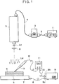
- FIG. 1 shows a constitutional view common to the use of an apparatus in first and second embodiments, in which an output of a laser power source 1 is connected via a connecting code 2 to input of a controller 3 for increasing or decreasing laser output, and an output of the controller 3 is connected via connecting code 4 to input of a laser oscillator 5.
- a lens 6 On output optical axis of the laser oscillator 5 is disposed a lens 6 for transforming a parallel light Lp output from the laser oscillator 5 to a diffused light Ld.
- a glass plate G and an Si substrate S to be bonded are securely placed on a platen 7 equipped with a heater for heating, the glass plate G being on top side.
- the platen 7 with heater is connected via a connecting code 8 to a positive electrode 9a of a DC power source 9 for bonding, a negative electrode 9b of which is connected via a connecting code 10 to a negative electrode of an ammeter 11.
- a positive electrode of the ammeter 11 is connected via a connecting code 12 to a needle electrode 13 made of tungsten, wherein a top end of the needle electrode 13 is placed into contact with the surface of the glass plate G.
- the laser oscillator 5 comprises a carbon dioxide laser having a wavelength of 10.6 ⁇ m
- the lens 6 comprises a convex lens made of Zn-Se.
- the laser power source 1 is turned on, and its output is regulated by the controller 3. Thereafter, infrared light is output from the laser oscillator 5.
- An output parallel light Lp is transformed to diffused light Ld by the lens 6, irradiating a plane of the glass plate G in contact with the Si substrate S.
- the DC power source 9 is turned on to apply a negative voltage to the needle electrode 13 and a positive voltage to the platen 7 with heater.
- the negative voltage is applied to the glass plate G and the positive voltage to the Si substrate S.
- an arrangement of the apparatus is the same as in Fig. 1, with the exception that the laser oscillator 5 comprises a helium-cadmium laser having a wavelength of 0.32 to 0.44 ⁇ m, and the lens 6 comprises a convex lens made of KDP.
- the laser power source 1 is turned on and adjusted by the controller 3.
- An ultraviolet light output from the laser oscillator 5 is diffused by the lens 6 and irradiated, while a negative voltage from the DC power source 9 is applied to the glass plate G, and a positive voltage to the Si substrate S.
- Fig. 2 shows a constitutional view of an apparatus in third embodiment, in which an output of a carbon dioxide laser power source 21 is connected via a connecting code 22 to input of a controller 23 for adjusting the laser output, and an output of the controller 23 is connected via a connecting code 24 to input of a carbon dioxide laser oscillator 25.
- a Zn-Se lens 26 On an output optical axis from the carbon dioxide laser oscillator 25 is disposed a Zn-Se lens 26 for transforming a parallel light Lp to diffused light Ld.
- a glass plate G and an Si substrate S to be bonded are disposed below the lens.
- an output of a helium-cadmium laser power source 27 is connected via a connecting code 28 to input of a controller 29 for adjusting the laser output, and an output of the controller 29 is connected via a connecting code 30 to input of a helium-cadmium laser oscillator 31.
- a KDP lens 32 On an output optical axis from the helium-cadmium laser oscillator 31 is disposed a KDP lens 32 for transforming a parallel light Lp to diffused light Ld.
- the glass plate G and the Si substrate S secured on a platen 33 without heater are disposed.
- the electrical connection concerning the glass plate G and the Si substrate S is the same as in the previous embodiment.
- a mask M made of tungsten having an aperture on the glass plate G so as to pass the irradiated light only through the aperture.
- the carbon dioxide laser power source 21 is turned on, and the laser output is adjusted by the controller 23, thereafter, infrared light is output from the carbon dioxide laser oscillator 25, and transformed to diffused light Ld by the Zn-Se lens 26 to irradiate the glass plate G.
- the helium-cadmium laser power source 27 is turned on, and the laser output is adjusted by the controller 29, thereafter, ultraviolet light is output from the helium-cadmium laser oscillator 31 and transformed to diffused light Ld by the KDP lens 32 to also irradiate the glass plate G.
- the DC power source 9 is turned on to apply a negative voltage via a needle electrode 13 to the glass plate G and a positive voltage via a platen 33 to the Si substrate S.
- infrared laser light of about 2W/cm2 and ultraviolet laser light of about 2W/cm2 were irradiated, while a voltage was applied to both end faces of the square glass plate G made of Pyrex glass #7740 0.5 mm thick and 10 mm square and the Si substrate S, and a voltage capable of flowing an electric current of about 2 ⁇ A was applied for ten minutes, so that the bonding between the glass plate G and the Si substrate S was allowed beneath the aperture of mask M. At this time, no bonding was made on a portion not irradiated by the laser beam because the light was shielded by the mask.
- the heating temperature was about 200°C, but may be set at different temperatures in view of the difference between thermal expansion coefficients without causing any trouble.
- the heating may be made to the degree not to obstruct the bonding due to the difference between thermal expansion coefficients, in order to improve reaction speed.
- a method for limiting the bonding portion may be realized by narrowing laser light flux to limit the irradiated area, instead of placing a mask M on the glass plate G.
- a soda silicate glass instead of using a Pyrex #7740 glass as the glass plate G, a soda silicate glass, for example, can be used with the same excellent bonding with the Si substrate S.
- a light is irradiated on a portion of the glass to be bonded with the electric conductor to lower the bonding temperature, whereby the bonding is relatively easily made even with different thermal expansion coefficients, also when there is a device arranged on the glass or electric conductor, no adverse effect is exerted to device characteristics due to high temperature. Further, it is possible to bond only a necessary portion by limiting irradiated area with a light-shielding mask.
- Fig. 3 is a view for explaining a fourth embodiment of the present invention.
- Fig. 3 is a view best depicting the features of this embodiment, in which reference numeral 101 is a Si substrate to be bonded, 102 is a light sensitive glass substrate to be bonded with the Si substrate, 106 is an electric conductive platen, 107 is a needle electrode electrically connecting to the Si substrate 101, 108 is a power source for applying a voltage between the Si substrate 101 and the light sensitive glass substrate 102, 109 is an electrode for the platen 106, 110 is a lead wire for the electrical connection between the needle electrode 107 and the power source 108, 111 is a lead wire for the electrical connection between the power source 108 and the electrode 109 of the platen 106, and 112 is a carbon dioxide laser for irradiating the light sensitive glass substrate 102 including a portion serving as the bonding interface between the Si substrate 101 and the light sensitive substrate 102.
- the light sensitive glass is one whose property permanently or reversibly changes upon i
- the Si substrate 101 and the light sensitive glass 102 are placed on the platen 106 with their bonding planes face to face. Further, after the needle electrode 107 is brought into contact with the surface of the Si substrate 101 for electrical connection, the power source 108 is turned on to apply a voltage between the Si substrate 101 and the light sensitive glass substrate 102. Further, irradiation of a laser light 112 is continued from above of the Si substrate 101 while the voltage is being applied. In this embodiment, heating by a heater or the like is unnecessary. In the above process, the bonding between the Si substrate 101 and the light sensitive glass 102 was made. PEG is employed as the light sensitive glass (PEG is a trade name by HOYA Corporation). Bonding conditions in this embodiment are as follows.
- Fig. 4 is a view for explaining a fifth embodiment of the present invention.
- Fig. 4 is a view best depicting the features of this embodiment, in which reference numeral 101 is a Si substrate for bonding, 102 is a light sensitive glass substrate for bonding with the Si substrate, 103 is a thin film electrode composed of Si thin film formed on a plane of the light sensitive glass substrate 102 opposite to and just above a bonding portion of the light sensitive glass substrate 102, 106 is an electric conductive platen, 107 is a needle electrode electrically connecting to the thin film electrode 103, 108 is a power source for applying a voltage between the Si substrate 101 and the light sensitive glass substrate 102, 109 is an electrode for the platen 106, 110 is a lead wire for electrical connection between the needle electrode 107 and the power source 108, 111 is a lead wire for electrical connection between the power source 108 and the electrode 109 of platen, and 112 is an excimer laser beam for irradiating the light sensitive glass substrate 102 including a
- a voltage is applied through the needle electrode 107 and the platen 106 between the thin film electrode 103 and the Si substrate 101 by the power source 108, after the Si substrate 101 and the light sensitive glass 102 are closely contacted face to face as shown in Fig. 4.
- the electric field is maximum near the bonding interface of the light sensitive glass 102 directly under the thin film electrode 103, i.e., near the bonding interface thinned at both end portions of the light sensitive glass 102 in Fig. 4. Accordingly, the bonding between the Si substrate 101 and the light sensitive substrate 102 can be easily made only at this portion where the electric field is maximum. That is, partial selective bonding between the Si substrate 101 and the light sensitive glass substrate 102 is possible.
- a (100) plane was a surface of the Si substrate, and a groove 105A on the Si substrate 101 was formed by electric field anisotropic etching using a KOH solution.
- Etching for forming thinned end portions of the light sensitive glass substrate 102 was accomplished by irradiating an excimer laser light through a mask (for shielding a laser beam) having an opening only at a portion to be thinned, thereafter performing the heat treatment (430°C x 2 hr.), and etching in 10% hydrogen fluoride solution. Note that a plane of the light sensitive glass substrate 102 on the side of bonding is not etched, because of a resist film applied, during the etching for formation of thinned portion.
- the resist film was eluted by acetone. And after washing, the thin film electrode 103 made of Si was formed using the mask having an opening only at thinned end portions of the light sensitive glass substrate 102.
- Bonding conditions in this embodiment are as follows.
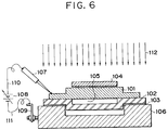
- Fig. 5 is a view for explaining a sixth embodiment of the present invention.
- Fig. 5 is a view best depicting the features of this embodiment, in which reference numeral 101 is a Si substrate for bonding, 102 is a light sensitive glass substrate for bonding with the Si substrate 101, 104 is a light shielding mask for shielding a laser beam so as to avoid the bonding of a laser shielded area, i.e., for the purpose of selective bonding, 105 is a groove provided on the light sensitive glass substrate 102, 106 is an electric conductive platen, 107 is a needle electrode electrically connectable to a thinned portion at both ends of the light sensitive glass 102, 108 is a power source for applying a voltage between the Si substrate 101 and the light sensitive glass substrate 102, 109 is an electrode for the platen 106, 110 is a lead wire for electrical connection between the needle electrode 107 and the power source 108, 111 is a lead wire for electrical connection between the power source 108 and the electrode 109
- the light shielding mask 104 is placed just above the groove 105 of the light sensitive glass substrate 102, after the Si substrate 101 and the light sensitive glass substrate 102 have been closely contacted face to face as shown in Fig. 5.
- the needle electrode 107 is electrically connected to a plane opposite and just above a bonding plane of the light sensitive glass 102, and a voltage is applied between the light sensitive glass substrate 102 and the Si substrate 101 by the power source 108.
- the electric field is maximum near the bonding interface in a thinned portion at both ends of the light sensitive glass.
- the light enters only the thinned portion at the both ends owing to the masking. Accordingly, the bonding between the Si substrate 101 and the light sensitive glass substrate 102 can be easily accomplished only at this portion where the electric field is maximum and the light enters. That is, partial selective bonding between the Si substrate 101 and the light sensitive glass substrate 102 is possible.
- a (100) plane was a surface of the Si substrate, and the formation of groove 105 on the light sensitive glass 102 and thinned portion at both ends thereof was performed in the same process as described in the fifth embodiment.
- Bonding conditions in this embodiment are as follows.
- the mask 104 was formed of a polymeric resist film, Al film, Au film, or Pt film, the bonding strength equivalent to that as above mentioned could be obtained.
- the same bonding of the materials i.e., the bonding between the light sensitive glass and the Si substrate was performed under the following conditions, using a conventional anodic bonding.
- a conventional anodic bonding As a result, there occurred peeling at a bonding portion during decreasing the bonding temperature to room temperature, thus the bonding could not be made.
- the light shielding mask 104 is placed on the surface of the Si substrate 101 just above the groove 105 of the light sensitive glass substrate 102, after the Si substrate 101 and the light sensitive glass substrate 102 have been closely contacted face to face as shown in Fig. 6. Further, the light sensitive glass 102 is aligned so that the platen 106 has no electrical connection except for the thin film electrode 103.
- a voltage is applied through the needle electrode 107 and the platen 106 between the Si substrate 101 and the thin film electrode 103 by the power source 108.
- the electric field is maximum at thinned end portions of the light sensitive glass substrate 102.
- the thinned end portions and their adjacent portions are only irradiated. Accordingly, the bonding between the Si substrate 101 and the light sensitive glass substrate 102 can be easily made only at those portions where the electric field is maximum and the light enters. That is, partial selective bonding between the Si substrate 101 and the light sensitive glass substrate 102 is possible.
- a (100)-plane was a surface of the Si substrate, and the formation of thinned portion at both ends thereof was performed in the same method as described in the fifth embodiment.
- the formation of the groove 105 of the light sensitive glass substrate 102 and the thin film electrode 103 was performed in the same process as in the fifth embodiment.
- Bonding conditions in this embodiment are as follows.
- the thin film electrode 103 was formed of an ITO film, a carbon film, an Al film, an Au film, or a Pt film, the bonding strength equivalent to that as above mentioned could be obtained.
- a bonded sample was cut with a disc cutter, but there was no peeling at the bonding interface.
- the bonding between the light sensitive glass and the electric conductor which have different thermal expansion coefficients can be easily made because of the capability of bonding at relatively low temperatures.
- a laser beam emitted from the laser oscillator is led through a lens or mirror into the vacuum atmosphere to irradiate the bonding portion, so that the bonding can be made without heating by a heater.
- the bonding between the Si substrate and the light sensitive glass substrate at a bonding portion like an opening of mask is also possible by using a mask for shielding the laser beam. That is, partial selective bonding is possible.
- Figs. 7, 8 and 9 are views for explaining a further embodiment of the present invention. These drawings are views best depicting the features of this embodiment, in which reference numeral 201 is a laser beam, 208 is an Si substrate, 209 is a glass (Pyrex glass) substrate for bonding with the Si substrate 208, 210 is an electric conductive film composed of an ITO film formed on the surface of the glass substrate 209, 211 is a platen composed of an electric conductor for laying thereon the Si substrate 208 and the glass substrate 209 which are connected with each other, 212, 213 are needle electrodes electrically connecting to electric conductive films 210 on the surfaces of the Si substrate 208 and the glass substrate 209, respectively, 213 is a needle electrode electrically connecting to the platen 211, 214 is a DC power source for applying an electric field between the Si substrate 208 and the glass substrate 209, 215 is a lead wire for electrical connection between the needle electrode 212 and the DC power source 214 and between the needle electrode 213 and the DC power source
- the Si substrate 208 was placed on the glass substrate 209, then a laser beam 201 was irradiated from the side of the Si substrate 208, while at the same time a voltage is applied between the Si substrate 208 and the glass substrate 209 by the power source 214 for about ten minutes. As a result, a bonding area 216 corresponding to an irradiation region of the laser beam 201 could be observed between the Si substrate 208 and the glass substrate 209.
- the glass and the laser beam used are as follows.
- the bonding when the bonding area is larger than a light flux area, the bonding can be made over the entire bonding area by scanning the laser beam.
- the Si film plane on a substrate having a Si film formed on the surface of an insulator such as glass or ceramics, instead of the Si substrate 208, with the glass substrate 209. That is, in this case, the Si film plane is electrically connected to the anode, and the electric conductive film 210 on the glass substrate 209 is electrically connected to the cathode. Thereafter, the laser beam is irradiated as a parallel flux from the glass substrate side to the bonding plane, while an electric field is being applied between the electrodes.
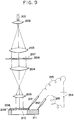
- Fig. 9 is a constitutional view of an overall apparatus in this embodiment.
- Reference numeral 201 is a laser beam
- 202, 203, 204 and 205 are lenses for enlarging and reducing the laser beam
- 206, 207 are a transparent glass to the laser beam 201 and a metallic film for reflecting the laser beam 201, which constitute a mask, respectively. Accordingly, the laser beam 201 can transmit through a portion where the metallic film 207 does not exist.
- 208 is a Si substrate for bonding
- 209 is a glass substrate for bonding with the Si substrate 208
- 210 is an electric conductive film composed of an ITO film formed on the surface of the glass substrate 209
- 211 is a platen for laying thereon the Si substrate 208 and the glass substrate 209 which are connected with each other
- 212 is a needle electrode electrically connecting to the surface of the Si substrate 208
- 213 is a needle electrode electrically connecting to the platen 211
- 214 is a DC power source for applying an electric field between the Si substrate 208 and the glass substrate 209
- 215 is a lead wire for electrical connection between the needle electrode 212 and the DC power source 214 and between the needle electrode 213 and the DC power source 214.
- the laser beam 201 is enlarged by the lens 202 and transformed into parallel rays by the lens 203, thereafter, the laser beam 201 passing through a pattern of the mask 207 is reduced by the lens 204 and further transformed into parallel rays by the lens 205, thereby irradiating a bonding portion between the Si substrate 208 and the glass substrate 209, while at the same time a voltage is applied between the Si substrate 208 and the glass substrate 209 by the DC power source 214.
- the laser beam 201 passing through the mask pattern 207 it becomes possible to lead the laser beam 201 passing through the mask pattern 207 to a local bonding portion between the Si substrate 208 and the glass substrate 209. While in the optical system as shown in Fig.
- a pattern projected onto the plane of a bonding sample is a reversal pattern of the mask 207, it will be appreciated that it can be made a normal pattern of the mask 207 by adding a lens (not shown) to the optical system, without deviating from scope of the present invention.
- the bonding between the Si substrate 208 having a plurality of concave grooves with a depth of 1000 ⁇ formed thereon and the flat plate-like glass substrate 209 was made by the anodic bonding with light irradiation, using a predetermined mask 207 having a pattern of preventing irradiation on the grooves. As a result, it could be found that the bonding was made only on a partial plane except for the concave grooves.
- Fig. 10 is a constitutional view of an apparatus in another embodiment of the present invention.
- Reference numeral 201 is a laser beam
- 202, 203, 204 and 205 are lenses for enlarging and reducing the laser beam
- 206, 207 are a transparent glass to the laser beam 201 and a metallic film for reflecting the laser beam 201, respectively, which constitute a mask. Accordingly, the laser beam 201 can transmit through a portion where the metallic film 207 does not exist.
- 208 is a Si substrate for bonding
- 209 is a glass substrate for bonding with the Si substrate 208
- 210 is an electric conductive film composed of an ITO film formed on the surface of the glass substrate 209
- 211 is a platen directly connected to a goniometer 222 for laying thereon the Si substrate 208
- 212 is a needle electrode electrically connecting to an electric conductive film 210 on the surface of the glass substrate 209
- 213 is an electrode electrically connecting to the platen 211
- 214 is a DC power source for applying an electric field between the Si substrate 208 and the glass substrate 209
- 215 is a lead wire for electrical connection between the needle electrode 212 and the DC power source 214 and between the electrode 213 and the DC power source 214
- 218 is a laser oscillator for oscillating the laser beam
- 219 is a laser transmitting window for the vacuum sealing composed of a transparent glass to the laser beam 201
- the Si substrate 208 is placed on the platen 211, and the glass substrate 209 is placed on the supporting plate 223, thereafter, the operator makes an alignment between the Si substrate 208 and the glass substrate 209 by using the light receiver 226 switched to a visible light mode and the monitor 230 with the remote operation (operating means not shown) from the, outside of the vacuum, as well as driving the goniometer 222, and then moves the supporting plate 223 downward by driving the motor 225 so as to bring the glass substrate 209 into slight contact with the Si substrate 208.
- the remote operation operating means not shown
- the laser beam 201 passing through the optical system (composed of lenses 202, 203, 204, 205) is irradiated on the Si substrate 208 and the glass substrate 209, while a voltage is applied between the Si substrate 208 and the glass substrate 209 by the DC power source 214.
- the bonding it is possible to detect a bonding portion between the Si substrate 208 and the glass substrate 209 by observing visually the information from the light receiver 226 switched to a laser light mode on the monitor television.
- the pattern projected on to the bonding sample is a reversal pattern of the mask 207
- the pattern projected on to the bonding sample is a reversal pattern of the mask 207
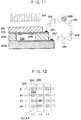
- Fig. 11 is a view for explaining a light sensor chip produced by using the anodic bonding with light irradiation according to an embodiment of the present invention.
- Reference numeral 201 is a laser beam
- 208 is a Si substrate
- 209 is a glass substrate for bonding with the Si substrate 208
- 210 is an electric conductive film composed of Si thin film formed on the glass substrate 251
- 214 is a DC power source for applying voltage between the electric conductive film 210 and an electric conductive layer 237
- 215 is a lead wire for electrical connection between the electric conductive film 210 and an ammeter 238, between the ammeter 238 and the DC power source 214, and between the DC power source 214 and the electric conductive layer 237
- 235 is vacuum chamber formed by bonding between the Si substrate 208, the glass substrate 209 and the upper lid glass substrate 251,
- 236 is a photoelectric film for emitting electrons with the irradiation of laser beam 201, 237 is an electric conductive layer which
- This chip is connected between the Si substrate 208 and the glass substrate 209, and between the glass substrate 209 and the Si thin film 210 on the upper cover glass 251, by the anodic bonding with light irradiation according to any one of the previous embodiments.
- this light sensor chip takes a matrix configuration as shown in Fig. 12, wherein Fig. 11 is a cross-sectional view of only a portion at a position (L2, l3) in Fig. 12.
- the ammeter 238 as well as its associated circuit are provided for each combination (L n , l n ) of electric conductive film in longitudinal and transversal directions.
- the laser beam 201 when the laser beam 201 is irradiated on the photoelectric film 236, produced electrons fly toward the electric conductive layer 237 which is an anode. At this time, the electric current will flow from the anode to the cathode. That is, the electric current will or will not flow depending on whether or not the laser beam 201 is irradiated on the photoelectric film 236. Accordingly, the laser irradiation at a position on the chip corresponding to each ammeter can be detected.
- a visible light beam is irradiated instead of the laser beam 201, it can be constructed so that the electric current may flow as in the above embodiment by changing the material of photoelectric film 236 (ex. multi alkali photoelectric plane).
- the anodic bonding with light irradiation according to the present invention capable of working at the low temperature without causing thermal expansion, is effective. Chips can be fabricated excellently with less internal stress. While the glass used in this embodiment was Pyrex glass, a light sensitive glass allows easier fabrication of the vacuum chambers.
- Fig. 13 is a view for explaining a light memory chip produced by using the anodic bonding with light irradiation according to an embodiment of the present invention.
- Reference numeral 201 is a laser beam
- 208 is a Si substrate
- 209 is a glass substrate for bonding with the Si substrate 208
- 210a is an electric conductive film (ITO film) formed in a groove 239 of the glass substrate 209
- 214 is a DC power source for applying voltage between the electric conductive film 210a and an electric conductive layer 237
- 215 is a lead wire for electrical connection between the electric conductive film 210a and an ammeter 238, between the ammeter 238 and the DC power source 214, and between the DC power source 214 and the electric conductive layer 237
- 237 is an electric conductive layer which is electrically insulated from the Si substrate 208 and formed by the doping of impurities
- 238 is an ammeter
- 239 is a groove formed on the glass substrate 209.
- the polarity of the DC power source 214 must be changed while the laser beam is being irradiated.
- the anodic bonding with light irradiation according to the present invention which does not cause thermal expansion, is effective. Chips will be fabricated excellently with less internal stress. Note that the glass used in this embodiment was Pyrex glass.
- the membrane 239 when pressure is applied on the membrane 239 from the external, the membrane 239 is warped inward or outward arcuately. That is, when external atmospheric pressure is higher than the pressure in the air-tight chamber 242, the membrane is warped inward, on contrary when atmospheric pressure is lower, the membrane is warped outward.
- the electric conductive film 241 moves closer to or away from the soft magnetic material 245, so that the change in eddy current occurs near the surface of the electric conductive film 241.
- the magnetic flux is changed by the change in eddy current, so that the electromotive force arising in the coil 249 is changed. It is possible to detect the external pressure by precalibrating the variation of electromotive force and the external pressure acting on the membrane 239.
- the air-tight chamber is fabricated at a known pressure, it is possible to determine the measured pressure with reference to such pressure of the air-tight chamber (however, under the environment where measured temperature is changed, calibration must be made for the amount of change in the measured temperature).
- the anodic bonding with light irradiation according to the present invention which does not cause thermal expansion, is effective in fabricating such a pressure sensor.
- a fabricated sensor allows to suppress the internal pressure and to perform more precise pressure sensing.
- the glass used in this embodiment is a light sensitive glass substrate.
- the Si substrate can be substituted by another material, for example, an electric conductor such as Al, Ta, Ti, Ni, Ge, GaAs, or Cr alloy, and the glass substrate can be substituted by another amorphous insulating material.
- an electric conductor such as Al, Ta, Ti, Ni, Ge, GaAs, or Cr alloy
- the glass substrate can be substituted by another amorphous insulating material.
- the light capable of transmitting through at least one of the materials may be irradiated from the side of that material, or by forming at least one of the materials to be thin sufficiently to transmit the light, the light may be irradiated from the side of that material.
Abstract
Description
- The present invention relates to an anodic bonding process for connecting together a glass and an electric conductor by applying a voltage therebetween, and an apparatus therefor.
- Conventionally, the anodic bonding between a glass and a silicon Si has been carried out by applying a voltage of about 300 V between the glass and Si, with Si as anode, while maintaining the temperature at about 400°C near a transition point of glass, as described by George Wallis and Daniel I. Pomerantz et al. in Journal of Applied Physics, vol. 40, no. 10, September 1969: Received 2 January 1969.
- However, in this conventional example, the bonding between the glass and Si is performed near a transition point of glass, so that thermal strain may possibly occur due to a difference between their thermal expansion coefficients when the temperature drops down to room temperature after the bonding at high temperature, resulting in a risk of peeling off. Therefore, it is required that the thermal expansion coefficients of glass and Si be equal in a wide range from room temperature to connexion temperature.
- A first object of the present invention is to provide an anodic bonding process which can resolve the above-mentioned drawback and allows the secure connexion without elevating the temperature to a transition point of glass.
- Fig. 1 is a constitutional view of an apparatus common to first and second embodiments.
- Fig. 2 is a constitutional view of an apparatus in third embodiment.
- Fig. 3 is a cross-sectional view of the bonding between an Si substrate and a photosensitive glass in fourth embodiment of the present invention.
- Fig. 4 is a cross-sectional view of the selective bonding between an Si substrate and a photosensitive glass in fifth embodiment of the present invention.
- Fig. 5 is a cross-sectional view of the selective bonding between an Si substrate and a photosensitive glass in sixth embodiment of the present invention.
- Fig. 6 is a cross-sectional view of the selective bonding between an Si substrate and a photosensitive glass in seventh embodiment of the present invention.
- Fig. 7 is a schematic view of the anodic bonding with light irradiation in eighth embodiment of the present invention.
- Fig. 8 is a view as looked from a direction of arrow A in Fig. 7.
- Fig. 9 is a schematic view of a laser optical system with mask allowing the use of the anodic bonding with light irradiation according to the present invention.
- Fig. 10 is a schematic view of a bonding apparatus allowing the use of the anodic bonding with light irradiation according to the present invention.
- Fig. 11 is an explanation view of a light sensor chip capable of being produced by using the anodic bonding with light irradiation according to the present invention.
- Fig. 12 is an explanation view from the top of a light sensor chip of Fig. 11.
- Fig. 13 is an explanation view of a light memory chip capable of being produced by using the anodic bonding with light irradiation according to the present invention.
- Fig. 14 is an explanation view from the top of a light sensor chip of Fig. 13.
- Fig. 15 is an explanation view of a pressure sensor capable of being produced by using the anodic bonding with light irradiation according to the present invention.
- The anodic bonding process in the preferred embodiments for anodic bonding made between a glass and an electric conductor, is characterized by applying a voltage between the glass and the electric conductor, while irradiating a light beam from the glass side or electric conductor side.
- The anodic bonding process using light irradiation with the above-mentioned constitution can be carried out by applying a voltage between the electric conductor and the glass, while a light beam is irradiated so as to relax a network structure of glass and to promote the diffusion of modifier ions in the glass, whereby the network structure of glass is relaxed at relatively low temperatures and modifier ions diffuse to cathode side to cause a great electrostatic attractive force between the electric conductor and the glass, so that the solid phase bonding is achieved.
- First, the principle of the anodic bonding process using the light irradiation will be described below.
- When a glass substrate and an Si substrate are to be joined by the anodic bonding, the network structure is relaxed by cutting weak binding portions in the network structure of glass or exciting it with oscillation, or modifier ions in the glass are diffused by giving an energy exceeding an activation energy for the diffusion of modifier ions. In order to have a certain directivity in the diffusion of modifier ions, voltage is applied between cathode of glass substrate and anode of Si substrate to generate an electric field. Thus, modifier ions are attracted to the cathode side and oxygen ions are attracted to the anode side, so that a depletion layer is produced near a bonding interface on the glass side, whereby a great electrostatic attractive force is generated between the glass substrate and the Si substrate. The gap between both substrates becomes atomic order due to this electrostatic attractive force, so that the solid phase bonding is possible.
- Since the network structure of glass is constructed of ionic bonds in various bond distances, there are some portions where relaxation occurs with relatively small external energy due to small bonding energy. Therefore, the network structure can be relaxed in the atmosphere at relatively low temperatures, without elevating the temperature to a softening point of glass as conventionally practiced, by irradiating infrared light as well as heating by a heater if necessary. Alternatively, when modifier ions are diffused, it is necessary to supply an activation energy in a magnitude of about 15 to 30 kcal/mol for diffusion of modifier ions from the outside. This energy corresponds to ultraviolet rays (wavelength 0.2 to 0.45 µm) in terms of the light energy, therefore, can be supplied by ultraviolet radiation. The network structure can be also relaxed by irradiating ultraviolet light to cut weak binding portions in the network structure of glass. In this case, though activation energy for diffusion of modifier ions may need to be supplied in a certain amount with heating by a heater, the bonding is possible at relatively low temperatures. Further, for example, by irradiating ultraviolet light together with infrared light in a combination, the anodic bonding can be performed without heating.
- This will be described in more detail.
- In the anodic bonding between glass substrate and Si substrate, it is possible to attract modifier ions to the cathode side and oxygen ions to the anode side by applying a voltage between the anode of Si substrate and the cathode of glass substrate under the condition without heating by a heater, while irradiating a light from side of the glass or the Si substrate so as to relax the network structure of glass and to promote the diffusion of modifier ions in the glass. Since a steep gradient in the electric field occurs near a bonding interface of glass due to the movement of modifier ions, a great electrostatic attractive force is produced at the interface between the glass substrate and the Si substrate. Owing to this electrostatic attractive force, the interval between the glass substrate and the Si substrate is gradually narrower, whereupon the solid phase bonding is achieved when the distance becomes atomic order.
- Accordingly, in order to promote the diffusion of modifier ions with the electric field, as above described, it is necessary to relax the network structure of glass as much as possible by cutting ionic bond at weak binding portions or exciting bonded ion with oscillation, or to supply an energy for further activating the diffusion of modifier ions from the outside.
- In general, the mobility of modifier ions in the glass, or the ionic conductivity, i.e., electric conductivity of glass δ can be expressed as follows:

Where δ is an electric conductivity of glass, R is a gas constant, T is a temperature, and ΔHdc is an activation energy for electric conduction. - Note that

- Accordingly, in the case of anodic bonding between the glass substrate and the Si substrate, in order to promote the movement of modifier ions in the glass under the condition without heating by a heater, i.e., at a bonding temperature T as low as possible, it is necessary to reduce a value of activation energy ΔHdc for electric conduction.
- Thus, in the present invention, the reduction of activation energy ΔHdc for electric conduction of glass is attempted by supplying the light energy as an ionic energy and an energy to expand the glass structure. For this reason, it is necessary to apply a voltage corresponding to the activation energy ΔHdc to both side faces of the glass substrate. Accordingly, the voltage is applied in a state that the bonding surfaces of the glass substrate and the Si substrate are closely contacted, whereby modifier ions in the glass substrate are diffused to the cathode side. As a result, an electrostatic attractive force contributing to the bonding is produced between the glass substrate and the Si substrate.
- On the other hand, since absorption of light depends on the quality and thickness of material and transmittancy of the light is reduced, it is desirable that the thicknesses of the glass substrate and the Si substrate are as thin as possible.
- The present process is such one that light is irradiated so as to relax the network structure as much as possible by cutting weak binding portions in the network structure of glass or exciting structural ions with oscillation, while applying an electric field between the glass substrate and the Si substrate. Therefore, the bonding between the glass substrate and the Si substrate is possible at lower temperatures, i.e., without heating by a heater. It will be appreciated that the bonding can be also made by the use of other electric conductors, instead of the Si substrate.
- Next, embodiments as illustrated in Figs. 1 and 2 will be described in detail. Fig. 1 shows a constitutional view common to the use of an apparatus in first and second embodiments, in which an output of a
laser power source 1 is connected via a connectingcode 2 to input of acontroller 3 for increasing or decreasing laser output, and an output of thecontroller 3 is connected via connectingcode 4 to input of alaser oscillator 5. On output optical axis of thelaser oscillator 5 is disposed a lens 6 for transforming a parallel light Lp output from thelaser oscillator 5 to a diffused light Ld. A glass plate G and an Si substrate S to be bonded are securely placed on aplaten 7 equipped with a heater for heating, the glass plate G being on top side. Theplaten 7 with heater is connected via a connectingcode 8 to apositive electrode 9a of aDC power source 9 for bonding, anegative electrode 9b of which is connected via a connectingcode 10 to a negative electrode of anammeter 11. A positive electrode of theammeter 11 is connected via a connectingcode 12 to aneedle electrode 13 made of tungsten, wherein a top end of theneedle electrode 13 is placed into contact with the surface of the glass plate G. - In the first embodiment, the
laser oscillator 5 comprises a carbon dioxide laser having a wavelength of 10.6 µm, and the lens 6 comprises a convex lens made of Zn-Se. In this constitution, thelaser power source 1 is turned on, and its output is regulated by thecontroller 3. Thereafter, infrared light is output from thelaser oscillator 5. An output parallel light Lp is transformed to diffused light Ld by the lens 6, irradiating a plane of the glass plate G in contact with the Si substrate S. At the same time, theDC power source 9 is turned on to apply a negative voltage to theneedle electrode 13 and a positive voltage to theplaten 7 with heater. Thus, the negative voltage is applied to the glass plate G and the positive voltage to the Si substrate S. - In this way, a voltage was applied to both faces of the glass plate G made of Pyrex glass #7740 (Pyrex is a trade name of Corning) 0.5 mm thick and 10 mm long and wide having a square shape and the Si substrate S, while infrared laser light having a strength of about 2W/cm² was irradiated. An electric current of about 4 µA flowed in a state that the
platen 7 with heater was heated up to a temperature of about 200°C. When the application of a voltage was continued for ten minutes while that current was maintained, the bonding between the glass plate G and the Si substrate S was achieved. However, when the laser light was not irradiated, the bonding was not enabled with the application of the same voltage. - In the second embodiment, an arrangement of the apparatus is the same as in Fig. 1, with the exception that the
laser oscillator 5 comprises a helium-cadmium laser having a wavelength of 0.32 to 0.44 µm, and the lens 6 comprises a convex lens made of KDP. Thelaser power source 1 is turned on and adjusted by thecontroller 3. An ultraviolet light output from thelaser oscillator 5 is diffused by the lens 6 and irradiated, while a negative voltage from theDC power source 9 is applied to the glass plate G, and a positive voltage to the Si substrate S. - As in the first embodiment, when ultraviolet laser light having a strength of about 2W/cm² was irradiated on the glass plate G made of Pyrex glass #7740 0.5 mm thick and 10 mm square and the Si substrate S, with the
platen 7 with heater heated up to about 200°C, and a voltage capable of flowing an electric current of about 4 µA was applied for ten minutes. The bonding between the glass plate G and the Si substrate S was enabled. However, when the laser light was not irradiated, the bonding was impossible with the application of the same voltage. Note that an ultraviolet light source such as a memory lamp can be also used instead of the helium-cadmium laser, with the same effects. - Fig. 2 shows a constitutional view of an apparatus in third embodiment, in which an output of a carbon dioxide
laser power source 21 is connected via a connectingcode 22 to input of acontroller 23 for adjusting the laser output, and an output of thecontroller 23 is connected via a connectingcode 24 to input of a carbondioxide laser oscillator 25. On an output optical axis from the carbondioxide laser oscillator 25 is disposed a Zn-Se lens 26 for transforming a parallel light Lp to diffused light Ld. A glass plate G and an Si substrate S to be bonded are disposed below the lens. On the other hand, an output of a helium-cadmiumlaser power source 27 is connected via a connectingcode 28 to input of acontroller 29 for adjusting the laser output, and an output of thecontroller 29 is connected via a connectingcode 30 to input of a helium-cadmium laser oscillator 31. On an output optical axis from the helium-cadmium laser oscillator 31 is disposed a KDP lens 32 for transforming a parallel light Lp to diffused light Ld. Below the lens, the glass plate G and the Si substrate S secured on aplaten 33 without heater are disposed. The electrical connection concerning the glass plate G and the Si substrate S is the same as in the previous embodiment. Also, there is provided a mask M made of tungsten having an aperture on the glass plate G so as to pass the irradiated light only through the aperture. - In this constitution, the carbon dioxide
laser power source 21 is turned on, and the laser output is adjusted by thecontroller 23, thereafter, infrared light is output from the carbondioxide laser oscillator 25, and transformed to diffused light Ld by the Zn-Se lens 26 to irradiate the glass plate G. At the same time, the helium-cadmiumlaser power source 27 is turned on, and the laser output is adjusted by thecontroller 29, thereafter, ultraviolet light is output from the helium-cadmium laser oscillator 31 and transformed to diffused light Ld by the KDP lens 32 to also irradiate the glass plate G. Further, at the same time, theDC power source 9 is turned on to apply a negative voltage via aneedle electrode 13 to the glass plate G and a positive voltage via aplaten 33 to the Si substrate S. - In this way, as in the first and second embodiments, infrared laser light of about 2W/cm² and ultraviolet laser light of about 2W/cm² were irradiated, while a voltage was applied to both end faces of the square glass plate G made of Pyrex glass #7740 0.5 mm thick and 10 mm square and the Si substrate S, and a voltage capable of flowing an electric current of about 2 µA was applied for ten minutes, so that the bonding between the glass plate G and the Si substrate S was allowed beneath the aperture of mask M. At this time, no bonding was made on a portion not irradiated by the laser beam because the light was shielded by the mask.
- In this way, by applying a voltage to the glass and the electric conductor while irradiating both ultraviolet light for relaxing the network structure of glass by cutting weak binding portions in the network structure and promoting the diffusion of modifier ions in the glass, and infrared light for relaxing the network structure by exciting ions of the network structure, the anodic bonding without heating becomes possible. In this case, a glass having modifier ion such as Na, Ca, Sr, Ba, Li, K, Rb, Cs, Fe, Be, Mg, Ni, Zn, Co, and Pb ions can obtain the same effects.
- While in the first and second embodiments as previously described, laser radiation was applied over the entire surface of the glass plate G, it should be noted that only a partial surface thereof can be bonded by using a mask M equivalent to that of the third embodiment to limit irradiated area. Also, the heating temperature was about 200°C, but may be set at different temperatures in view of the difference between thermal expansion coefficients without causing any trouble.
- Also, while in the third embodiment the heating is not made, the heating may be made to the degree not to obstruct the bonding due to the difference between thermal expansion coefficients, in order to improve reaction speed. A method for limiting the bonding portion may be realized by narrowing laser light flux to limit the irradiated area, instead of placing a mask M on the glass plate G. In the described embodiments, instead of using a Pyrex #7740 glass as the glass plate G, a soda silicate glass, for example, can be used with the same excellent bonding with the Si substrate S.
- As above described, according to the anodic bonding process using light irradiation in the above embodiments, a light is irradiated on a portion of the glass to be bonded with the electric conductor to lower the bonding temperature, whereby the bonding is relatively easily made even with different thermal expansion coefficients, also when there is a device arranged on the glass or electric conductor, no adverse effect is exerted to device characteristics due to high temperature. Further, it is possible to bond only a necessary portion by limiting irradiated area with a light-shielding mask.
- In the following, another embodiment will be described.
- Fig. 3 is a view for explaining a fourth embodiment of the present invention. Fig. 3 is a view best depicting the features of this embodiment, in which reference numeral 101 is a Si substrate to be bonded, 102 is a light sensitive glass substrate to be bonded with the Si substrate, 106 is an electric conductive platen, 107 is a needle electrode electrically connecting to the
Si substrate Si substrate 101 and the lightsensitive glass substrate platen needle electrode 107 and thepower source power source 108 and theelectrode 109 of theplaten sensitive glass substrate 102 including a portion serving as the bonding interface between theSi substrate 101 and the lightsensitive substrate 102. The light sensitive glass is one whose property permanently or reversibly changes upon irradiation. - In the above constitution, the
Si substrate 101 and the lightsensitive glass 102 are placed on theplaten 106 with their bonding planes face to face. Further, after theneedle electrode 107 is brought into contact with the surface of theSi substrate 101 for electrical connection, thepower source 108 is turned on to apply a voltage between theSi substrate 101 and the lightsensitive glass substrate 102. Further, irradiation of alaser light 112 is continued from above of theSi substrate 101 while the voltage is being applied. In this embodiment, heating by a heater or the like is unnecessary. In the above process, the bonding between theSi substrate 101 and the lightsensitive glass 102 was made. PEG is employed as the light sensitive glass (PEG is a trade name by HOYA Corporation). Bonding conditions in this embodiment are as follows. - Size of Si (100) substrate:
- 26 mm x 38 mm x 0.5 mm (thickness)
- Size of light sensitive glass:
- 30 mm x 42 mm x 1 mm (thickness) (PEG glass made by HOYA Corporation)
- Applied voltage:
- 1.2 kV
- Laser beam:
- Carbon dioxide laser (≃ 5W/cm²)
- Time:
- ten minutes per spot
- Area per spot of laser beam:
- ≃ 1 cm²
- Fig. 4 is a view for explaining a fifth embodiment of the present invention. Fig. 4 is a view best depicting the features of this embodiment, in which reference numeral 101 is a Si substrate for bonding, 102 is a light sensitive glass substrate for bonding with the Si substrate, 103 is a thin film electrode composed of Si thin film formed on a plane of the light
sensitive glass substrate 102 opposite to and just above a bonding portion of the lightsensitive glass substrate thin film electrode Si substrate 101 and the lightsensitive glass substrate platen needle electrode 107 and thepower source power source 108 and theelectrode 109 of platen, and 112 is an excimer laser beam for irradiating the lightsensitive glass substrate 102 including a portion serving as the bonding interface between theSi substrate 101 and the lightsensitive substrate 102. A KrF laser (wavelength of 246 mm) which was a rare gas halide laser was employed as the excimer laser light source. - In the above consitution, a voltage is applied through the
needle electrode 107 and theplaten 106 between thethin film electrode 103 and theSi substrate 101 by thepower source 108, after theSi substrate 101 and the lightsensitive glass 102 are closely contacted face to face as shown in Fig. 4. By the application of the voltage, the electric field is maximum near the bonding interface of the lightsensitive glass 102 directly under thethin film electrode 103, i.e., near the bonding interface thinned at both end portions of the lightsensitive glass 102 in Fig. 4. Accordingly, the bonding between theSi substrate 101 and the lightsensitive substrate 102 can be easily made only at this portion where the electric field is maximum. That is, partial selective bonding between theSi substrate 101 and the lightsensitive glass substrate 102 is possible. - In this embodiment, a (100) plane was a surface of the Si substrate, and a
groove 105A on theSi substrate 101 was formed by electric field anisotropic etching using a KOH solution. Etching for forming thinned end portions of the lightsensitive glass substrate 102 was accomplished by irradiating an excimer laser light through a mask (for shielding a laser beam) having an opening only at a portion to be thinned, thereafter performing the heat treatment (430°C x 2 hr.), and etching in 10% hydrogen fluoride solution. Note that a plane of the lightsensitive glass substrate 102 on the side of bonding is not etched, because of a resist film applied, during the etching for formation of thinned portion. After the etching for formation of thinned portion, the resist film was eluted by acetone. And after washing, thethin film electrode 103 made of Si was formed using the mask having an opening only at thinned end portions of the lightsensitive glass substrate 102. - Bonding conditions in this embodiment are as follows.
- Size of Si (100) substrate:
- 26 mm x 38 mm x 0.5 mm (thickness)
- with size of
groove 105A: - 26 mm x 18 mm x 0.2 mm (depth of groove)
- Size of light sensitive glass substrate:
- 30 mm x 42 mm x 1.0 mm (thickness) (PEG glass made by HOYA Corporation) with sheet thickness of thinned portion at
- both ends:
- 0.4 mm
- Thickness of thin film electrode:
- 1000 Å
- Applied voltage:
- 500 V
- Laser beam:
- Excimer laser (≃ 1.5W/cm²)
- Time:
- ten minutes per spot
- Area per spot of laser beam:
- ≃ 0.5 cm²
- Fig. 5 is a view for explaining a sixth embodiment of the present invention. Fig. 5 is a view best depicting the features of this embodiment, in which reference numeral 101 is a Si substrate for bonding, 102 is a light sensitive glass substrate for bonding with the
Si substrate sensitive glass substrate sensitive glass Si substrate 101 and the lightsensitive glass substrate platen needle electrode 107 and thepower source power source 108 and theelectrode 109 of theplaten sensitive glass substrate 102 including a portion serving as the bonding interface between theSi substrate 101 and the lightsensitive substrate 102. - In the above constitution, the
light shielding mask 104 is placed just above thegroove 105 of the lightsensitive glass substrate 102, after theSi substrate 101 and the lightsensitive glass substrate 102 have been closely contacted face to face as shown in Fig. 5. Theneedle electrode 107 is electrically connected to a plane opposite and just above a bonding plane of the lightsensitive glass 102, and a voltage is applied between the lightsensitive glass substrate 102 and theSi substrate 101 by thepower source 108. By the application of the voltage, the electric field is maximum near the bonding interface in a thinned portion at both ends of the light sensitive glass. The light enters only the thinned portion at the both ends owing to the masking. Accordingly, the bonding between theSi substrate 101 and the lightsensitive glass substrate 102 can be easily accomplished only at this portion where the electric field is maximum and the light enters. That is, partial selective bonding between theSi substrate 101 and the lightsensitive glass substrate 102 is possible. - In this embodiment, a (100) plane was a surface of the Si substrate, and the formation of
groove 105 on the lightsensitive glass 102 and thinned portion at both ends thereof was performed in the same process as described in the fifth embodiment. - Bonding conditions in this embodiment are as follows.
- Size of Si (100) substrate:
- 26 mm x 38 mm x 0.5 mm (thickness)
- Size of light sensitive glass:
- 30 mm x 42 mm x 1.0 mm (thickness) (PEG glass made by HOYA Corporation)
- with size of groove 105:
- 30 mm x 22 mm x 0.5 mm (depth) with sheet thickness of thinned portion at
- both ends:
- 0.4 mm
- Applied voltage:
- 500 V
- Laser beam:
- Carbon dioxide laser (≃ 5W/cm²)
- Time:
- ten minutes per spot
- Mask:
- Al plate
- Area per spot of laser beam:
- ≃ 1 cm²
- Note that when the
mask 104 was formed of a polymeric resist film, Al film, Au film, or Pt film, the bonding strength equivalent to that as above mentioned could be obtained. - On the other hand, the same bonding of the materials, i.e., the bonding between the light sensitive glass and the Si substrate was performed under the following conditions, using a conventional anodic bonding. As a result, there occurred peeling at a bonding portion during decreasing the bonding temperature to room temperature, thus the bonding could not be made.
- Conditions for conventional anodic bonding experiment:
- Bonding material:
- Light sensitive glass (PEG glass made by HOYA Corporation)/Si(100)
- Temperature:
- 350°C
- Applied voltage:
- 500 V
- Bonding time:
- forty minutes
- In the above constitution, the
light shielding mask 104 is placed on the surface of theSi substrate 101 just above thegroove 105 of the lightsensitive glass substrate 102, after theSi substrate 101 and the lightsensitive glass substrate 102 have been closely contacted face to face as shown in Fig. 6. Further, the lightsensitive glass 102 is aligned so that theplaten 106 has no electrical connection except for thethin film electrode 103. A voltage is applied through theneedle electrode 107 and theplaten 106 between theSi substrate 101 and thethin film electrode 103 by thepower source 108. By the application of the voltage, the electric field is maximum at thinned end portions of the lightsensitive glass substrate 102. The thinned end portions and their adjacent portions are only irradiated. Accordingly, the bonding between theSi substrate 101 and the lightsensitive glass substrate 102 can be easily made only at those portions where the electric field is maximum and the light enters. That is, partial selective bonding between theSi substrate 101 and the lightsensitive glass substrate 102 is possible. - In this embodiment, a (100)-plane was a surface of the Si substrate, and the formation of thinned portion at both ends thereof was performed in the same method as described in the fifth embodiment. The formation of the
groove 105 of the lightsensitive glass substrate 102 and thethin film electrode 103 was performed in the same process as in the fifth embodiment. - Bonding conditions in this embodiment are as follows.
- Size of Si (100) substrate:
- 26 mm x 38 mm x 0.5 mm (thickness) with sheet thickness of thinned portion at both ends: 0.3 mm
- Size of light sensitive glass substrate 102:
- 30 mm x 42 mm x 1.0 mm (thickness) (PEG glass made by HOYA Corporation)
- with size of groove 105:
- 30 mm x 22 mm x 0.5 mm (depth)
- with sheet thickness of thinned portion at both ends:
- 0.5 mm
- Applied voltage:
- 400 V
- Laser beam:
- Carbon dioxide laser (≃ 5W/cm²)
- Time:
- ten minutes per spot
- Mask:
- Al plate
- Area per spot of laser beam:
- ≃ 1 cm²
- Note that when the
thin film electrode 103 was formed of an ITO film, a carbon film, an Al film, an Au film, or a Pt film, the bonding strength equivalent to that as above mentioned could be obtained. A bonded sample was cut with a disc cutter, but there was no peeling at the bonding interface. - As above described, with the anodic bonding using light irradiation, the bonding between the light sensitive glass and the electric conductor which have different thermal expansion coefficients can be easily made because of the capability of bonding at relatively low temperatures. Further, when the bonding between the Si substrate and the light sensitive glass is made in a vacuum atmosphere, a laser beam emitted from the laser oscillator is led through a lens or mirror into the vacuum atmosphere to irradiate the bonding portion, so that the bonding can be made without heating by a heater. Further the bonding between the Si substrate and the light sensitive glass substrate at a bonding portion like an opening of mask is also possible by using a mask for shielding the laser beam. That is, partial selective bonding is possible.
- Figs. 7, 8 and 9 are views for explaining a further embodiment of the present invention. These drawings are views best depicting the features of this embodiment, in which reference numeral 201 is a laser beam, 208 is an Si substrate, 209 is a glass (Pyrex glass) substrate for bonding with the
Si substrate glass substrate Si substrate 208 and theglass substrate 209 which are connected with each other, 212, 213 are needle electrodes electrically connecting to electricconductive films 210 on the surfaces of theSi substrate 208 and theglass substrate 209, respectively, 213 is a needle electrode electrically connecting to theplaten Si substrate 208 and theglass substrate needle electrode 212 and theDC power source 214 and between theneedle electrode 213 and theDC power source Si substrate 208 and theglass substrate 209. - In the above constitution, the
Si substrate 208 was placed on theglass substrate 209, then alaser beam 201 was irradiated from the side of theSi substrate 208, while at the same time a voltage is applied between theSi substrate 208 and theglass substrate 209 by thepower source 214 for about ten minutes. As a result, abonding area 216 corresponding to an irradiation region of thelaser beam 201 could be observed between theSi substrate 208 and theglass substrate 209. - Note that in this embodiment the glass and the laser beam used are as follows.
- Glass:
- Pyrex glass 0.5 mm thick
- Thickness of Si substrate:
- 0.5 mm
- Laser:
- CO₂ laser beam 6W/cm²
- On the other hand, in Fig. 7, when the bonding area is larger than a light flux area, the bonding can be made over the entire bonding area by scanning the laser beam.
- Further, it is possible to bond the Si film plane on a substrate having a Si film formed on the surface of an insulator such as glass or ceramics, instead of the
Si substrate 208, with theglass substrate 209. That is, in this case, the Si film plane is electrically connected to the anode, and the electricconductive film 210 on theglass substrate 209 is electrically connected to the cathode. Thereafter, the laser beam is irradiated as a parallel flux from the glass substrate side to the bonding plane, while an electric field is being applied between the electrodes. - Fig. 9 is a constitutional view of an overall apparatus in this embodiment.
Reference numeral 201 is a laser beam, 202, 203, 204 and 205 are lenses for enlarging and reducing the laser beam, and 206, 207 are a transparent glass to thelaser beam 201 and a metallic film for reflecting thelaser beam 201, which constitute a mask, respectively. Accordingly, thelaser beam 201 can transmit through a portion where themetallic film 207 does not exist. 208 is a Si substrate for bonding, 209 is a glass substrate for bonding with theSi substrate glass substrate Si substrate 208 and theglass substrate 209 which are connected with each other, 212 is a needle electrode electrically connecting to the surface of theSi substrate platen Si substrate 208 and theglass substrate needle electrode 212 and theDC power source 214 and between theneedle electrode 213 and theDC power source 214. - In the above constitution, the
laser beam 201 is enlarged by thelens 202 and transformed into parallel rays by thelens 203, thereafter, thelaser beam 201 passing through a pattern of themask 207 is reduced by thelens 204 and further transformed into parallel rays by thelens 205, thereby irradiating a bonding portion between theSi substrate 208 and theglass substrate 209, while at the same time a voltage is applied between theSi substrate 208 and theglass substrate 209 by theDC power source 214. With the above optical system, it becomes possible to lead thelaser beam 201 passing through themask pattern 207 to a local bonding portion between theSi substrate 208 and theglass substrate 209. While in the optical system as shown in Fig. 9, a pattern projected onto the plane of a bonding sample (Si substrate 208/glass substrate 209) is a reversal pattern of themask 207, it will be appreciated that it can be made a normal pattern of themask 207 by adding a lens (not shown) to the optical system, without deviating from scope of the present invention. In this embodiment, the bonding between theSi substrate 208 having a plurality of concave grooves with a depth of 1000 Å formed thereon and the flat plate-like glass substrate 209 was made by the anodic bonding with light irradiation, using apredetermined mask 207 having a pattern of preventing irradiation on the grooves. As a result, it could be found that the bonding was made only on a partial plane except for the concave grooves. - Fig. 10 is a constitutional view of an apparatus in another embodiment of the present invention.
Reference numeral 201 is a laser beam, 202, 203, 204 and 205 are lenses for enlarging and reducing the laser beam, and 206, 207 are a transparent glass to thelaser beam 201 and a metallic film for reflecting thelaser beam 201, respectively, which constitute a mask. Accordingly, thelaser beam 201 can transmit through a portion where themetallic film 207 does not exist. 208 is a Si substrate for bonding, 209 is a glass substrate for bonding with the Si substrate 208, 210 is an electric conductive film composed of an ITO film formed on the surface of the glass substrate 209, 211 is a platen directly connected to a goniometer 222 for laying thereon the Si substrate 208, and the glass substrate 209 which are connected with each other, 212 is a needle electrode electrically connecting to an electric conductive film 210 on the surface of the glass substrate 209, 213 is an electrode electrically connecting to the platen 211, 214 is a DC power source for applying an electric field between the Si substrate 208 and the glass substrate 209, and 215 is a lead wire for electrical connection between the needle electrode 212 and the DC power source 214 and between the electrode 213 and the DC power source 214, 218 is a laser oscillator for oscillating the laser beam, 219 is a laser transmitting window for the vacuum sealing composed of a transparent glass to the laser beam 201, 220 is a laser transmitting window frame, 221 is a bottom plate of a vacuum apparatus connected to the laser transmitting window frame 220, 222 is an electrically driven goniometer (wiring not shown) movable in X-Y directions which is connected to the bottom plate 221 of the vacuum apparatus, 223 is a supporting plate for supporting the glass substrate 209, 224 is a rotary screw for moving the supporting plate 223 upward or downward, 225 is a motor (wiring not shown) for driving the supporting plate 223 upward or downward by rotating the rotary screw in a clockwise or counterclockwise direction, respectively, 226 is a light receiver for receiving the laser beam 201 transmitting through the Si substrate 208 and the glass substrate 209 which are connected, 227 is an arm for mounting the light receiver, 228 is a lead wire for the electrical connection from the light receiver 226 to a monitor television 230, 229 is a vacuum introducing electrode terminal for the electrical connection between a vacuum bath 231 and the atmosphere, 230 is a monitor television for viewing the information received by the light receiver 226, 231 is a vacuum bath for enabling the bonding between the Si substrate 208 and the glass substrate 209 in a vacuum, 232 is a bell jar for forming the vacuum bath and constructed detachably, 233 is a vacuum pump, and 234 is a skirted frame for supporting the vacuum bath 231 and accommodating a laser optical system as well as the vacuum pump 233. - The bonding principle of this apparatus is the same as shown in Fig. 9.
- In the above constitution, the
Si substrate 208 is placed on theplaten 211, and theglass substrate 209 is placed on the supportingplate 223, thereafter, the operator makes an alignment between theSi substrate 208 and theglass substrate 209 by using thelight receiver 226 switched to a visible light mode and themonitor 230 with the remote operation (operating means not shown) from the, outside of the vacuum, as well as driving thegoniometer 222, and then moves the supportingplate 223 downward by driving themotor 225 so as to bring theglass substrate 209 into slight contact with theSi substrate 208. Thereafter, thelaser beam 201 passing through the optical system (composed oflenses Si substrate 208 and theglass substrate 209, while a voltage is applied between theSi substrate 208 and theglass substrate 209 by theDC power source 214. During the bonding, it is possible to detect a bonding portion between theSi substrate 208 and theglass substrate 209 by observing visually the information from thelight receiver 226 switched to a laser light mode on the monitor television. - With the provision of a mechanism (not shown) for moving the
mask 206 forward and backward, leftward and rightward, it is possible to make the bonding between theSi substrate 208 having a bonding portion which is similar to mask pattern, and theglass substrate 209. That is, it is possible to form a plurality of bonding portions having the same shape as the Si substrate or glass substrate by the step and repeat. - While in the optical system as shown in Fig. 10, the pattern projected on to the bonding sample (
Si substrate 208/glass substrate 209) is a reversal pattern of themask 207, it will be appreciated that it can be made a normal pattern of themask 207 by adding a lens (not shown) to the optical system, without deviating from scope of the present invention. - Fig. 11 is a view for explaining a light sensor chip produced by using the anodic bonding with light irradiation according to an embodiment of the present invention.
Reference numeral 201 is a laser beam, 208 is a Si substrate, 209 is a glass substrate for bonding with theSi substrate glass substrate conductive film 210 and an electricconductive layer conductive film 210 and anammeter 238, between theammeter 238 and theDC power source 214, and between theDC power source 214 and the electricconductive layer Si substrate 208, theglass substrate 209 and the upperlid glass substrate laser beam Si substrate 208 and formed by the doping of impurities, 238 is an ammeter for detecting the electric current produced by electrons flying from thephotoelectric film 236 to the electricconductive layer glass substrate 209. - This chip is connected between the
Si substrate 208 and theglass substrate 209, and between theglass substrate 209 and the Sithin film 210 on theupper cover glass 251, by the anodic bonding with light irradiation according to any one of the previous embodiments. - Note that this light sensor chip takes a matrix configuration as shown in Fig. 12, wherein Fig. 11 is a cross-sectional view of only a portion at a position (L₂, l₃) in Fig. 12. The
ammeter 238 as well as its associated circuit are provided for each combination (Ln, ln) of electric conductive film in longitudinal and transversal directions. - In the above constitution, when the
laser beam 201 is irradiated on thephotoelectric film 236, produced electrons fly toward the electricconductive layer 237 which is an anode. At this time, the electric current will flow from the anode to the cathode. That is, the electric current will or will not flow depending on whether or not thelaser beam 201 is irradiated on thephotoelectric film 236. Accordingly, the laser irradiation at a position on the chip corresponding to each ammeter can be detected. When a visible light beam is irradiated instead of thelaser beam 201, it can be constructed so that the electric current may flow as in the above embodiment by changing the material of photoelectric film 236 (ex. multi alkali photoelectric plane). - In the case of producing an element composed of fine vacuum chambers capable of converting the light into an electric signal as above described, the anodic bonding with light irradiation according to the present invention, capable of working at the low temperature without causing thermal expansion, is effective. Chips can be fabricated excellently with less internal stress. While the glass used in this embodiment was Pyrex glass, a light sensitive glass allows easier fabrication of the vacuum chambers.
- Fig. 13 is a view for explaining a light memory chip produced by using the anodic bonding with light irradiation according to an embodiment of the present invention.
Reference numeral 201 is a laser beam, 208 is a Si substrate, 209 is a glass substrate for bonding with theSi substrate groove 239 of theglass substrate conductive film 210a and an electricconductive layer conductive film 210a and anammeter 238, between theammeter 238 and theDC power source 214, and between theDC power source 214 and the electricconductive layer Si substrate 208 and formed by the doping of impurities, 238 is an ammeter, and 239 is a groove formed on theglass substrate 209. - This chip is bonded between the
Si substrate 208 and theglass substrate 209 by the anodic bonding with light irradiation according to any one of the previous embodiments. This sensor chip also takes a matrix configuration as shown in Fig. 14, wherein Fig. 13 is a cross-sectional view of only a portion at a position (L₄, l₂) in Fig. 14. Theammeter 238 as well as its associated circuit are provided for each combination (Ln, ln) of the electric conductive film in longitudinal and transversal directions. - In the above constitution, when the
laser beam 201 is irradiated on thegroove 239, impurity ions composed of cations of theglass 209 are more likely to move toward the electricconductive film 210a which is a cathode. That is, ionic electric current will instantaneously flow from the anode to the cathode. Next, when the laser beam is once interrupted and then the laser beam is irradiated again toward thegroove 239 as above described, the ionic electric current does not flow. Thus, in order to flow the ionic electric current again, i.e., to refresh, when thelaser beam 201 is irradiated on thegroove 239 as above described, the polarity of theDC power source 214 must be changed while the laser beam is being irradiated. - In fabricating a micro device as above described which serves as a memory, the anodic bonding with light irradiation according to the present invention, which does not cause thermal expansion, is effective. Chips will be fabricated excellently with less internal stress. Note that the glass used in this embodiment was Pyrex glass.
- The method of examining whether or not the light is irradiated on each matrix point, i.e., the reading of information, can be accomplished in the following way.
- 1. A voltage is applied to each matrix point while the light is irradiated on each matrix.
- (a) At this time, matrix point where ionic current have flowed means that light is not irradiated in advance, namely it is not memorized.
- (b) On the contrary, the matrix point where ionic current have hardly flowed means that light is irradiated in advance, namely, it is memorized.
- 2. Accordingly, it is possible to read the memory all over the matrix points when each matrix point is examined for electric conduction thereof by applying a voltage between electrodes constituting the matrix, i.e., between Lm-ln (m=l-M, n=l-N for a matrix of MxN) in a certain sequence.
- 3. When the memory is still stored after reading, the following operation is performed. That is only in matrix points not memorized, the polarity between electrodes constituting the matrix is reversed immediately after reading, while irradiation is continued. Through this operation, ions in the matrix point can be returned to their original position.
- Fig. 15 is a view for explaining a pressure sensor produced by using the anodic bonding with light irradiation according to an embodiment of the present invention.
Reference numeral 208 is a Si substrate, 209 is a glass substrate (light sensitive glass) for bonding with theSi substrate Si substrate glass substrate glass substrate magnetic material 245 to thedeep groove portion magnetic material magnetic material Si substrate 208 and theglass substrate 209 is made by using the anodic bonding with light irradiation according to any one of the previous embodiments. - Next, in the above constitution, when pressure is applied on the
membrane 239 from the external, themembrane 239 is warped inward or outward arcuately. That is, when external atmospheric pressure is higher than the pressure in the air-tight chamber 242, the membrane is warped inward, on contrary when atmospheric pressure is lower, the membrane is warped outward. At this time, the electricconductive film 241 moves closer to or away from the softmagnetic material 245, so that the change in eddy current occurs near the surface of the electricconductive film 241. The magnetic flux is changed by the change in eddy current, so that the electromotive force arising in thecoil 249 is changed. It is possible to detect the external pressure by precalibrating the variation of electromotive force and the external pressure acting on themembrane 239. Further, when the air-tight chamber is fabricated at a known pressure, it is possible to determine the measured pressure with reference to such pressure of the air-tight chamber (however, under the environment where measured temperature is changed, calibration must be made for the amount of change in the measured temperature). The anodic bonding with light irradiation according to the present invention, which does not cause thermal expansion, is effective in fabricating such a pressure sensor. A fabricated sensor allows to suppress the internal pressure and to perform more precise pressure sensing. Note that the glass used in this embodiment is a light sensitive glass substrate. - Note that in the above embodiments, the Si substrate can be substituted by another material, for example, an electric conductor such as Al, Ta, Ti, Ni, Ge, GaAs, or Cr alloy, and the glass substrate can be substituted by another amorphous insulating material. In these cases, to transmit the light to a bonded face, the light capable of transmitting through at least one of the materials may be irradiated from the side of that material, or by forming at least one of the materials to be thin sufficiently to transmit the light, the light may be irradiated from the side of that material.
- Disclosed is a process and an apparatus for anodic bonding, in which Si substrate and glass substrate are contacted each other, a voltage is applied therebetween, and then light is irradiated on a contact portion thereof, whereby the Si substrate and the glass substrate are bonded at a lower temperature than transition temperature of the glass substrate.
Claims (28)
- A process for anodic bonding between an electric conductor and an amorphous insulator, comprising the steps of:
placing said electric conductor into contact with said amorphous insulator;
applying a voltage between said contacted electric conductor and amorphous insulator; and
irradiating a light flux through an illumination optical system toward a contact portion between said contacted electric conductor and amorphous insulator;
wherein said electric conductor and said amorphous insulator are bonded at a lower temperature than a transition temperature of said amorphous insulator in said voltage applying step and said light flux irradiating step. - A process according to claim 1, wherein the irradiating light flux in said irradiating step is a light beam having a wavelength for exciting ions in network structure of said amorphous insulator.
- A process according to claim 1, wherein the irradiating light flux in said irradiating step is an infrared light having a wavelength in the range of 1.0 to 12 µm.
- A process according to claim 1, wherein the irradiating light flux in said irradiating step is a light beam having a wavelength for acting to cut a connection in network structure of said amorphous insulator.
- A process according to claim 1, wherein the irradiating light flux in said irradiating step is an ultraviolet light having a wavelength in the range of 0.2 to 0.45 µm.
- A process according to claim 1, wherein the irradiating light flux in said irradiating step is an ultraviolet light and an infrared light which are irradiated simultaneously.
- A process according to claim 6, wherein said ultraviolet light in said irradiating step relaxes said network structure by cutting the connection in said network structure of said amorphous insulator, while said infrared light relaxes said network structure by oscillationally exciting ions in said network structure of said amorphous insulator to promote diffusion of modifier ions in said amorphous insulator.
- A process according to claim 1, wherein said electric conductor comprises Si.
- A process according to claim 1, wherein said amorphous insulator comprises a heat-resistant glass.
- A process according to claim 1, wherein said amorphous insulator comprises a soda-silicate glass.
- A process according to claim 1, wherein said amorphous insulator comprises a light sensitive glass.
- A process according to claim 1, further comprising a masking step of preventing the irradiation of light flux except for a contact portion to be anodic bonded between said electric conductor and said amorphous insulator in said irradiating step.
- A process according to claim 1, wherein a predetermined pattern is projected in said irradiating step so that irradiation of light flux except for a contact portion to be anodic bonded between said electric conductor and said amorphous insulator is prevented.
- A process according to claim 1, further comprising the step of arranging a voltage application electrode only at back side of a portion to be anodic bonded of said amorphous insulator.
- A process according to claim 1, wherein the light flux is irradiated only to a contact portion to be anodic bonded between said electric conductor and said amorphous insulator in said irradiating step.
- An apparatus for anodic bonding between an electric conductor and an amorphous insulator, comprising:
a support table for arranging said electric conductor and said amorphous insulator each contacted, at a predetermined position;
a voltage application circuit for applying a voltage between said contacted electric conductor and amorphous insulator;
a light source; and
an illumination optical system for irradiating a light flux from said light source toward a contact portion between said contacted electric conductor and amorphous insulator;
wherein said electric conductor and said amorphous insulator are bonded at a lower temperature than a transition temperature of said amorphous insulator by applying the voltage with said voltage application means and irradiating the light flux by the illumination system. - An apparatus according to claim 16, wherein said illumination system comprises:
mask holding means for arranging a mask having a pattern corresponding to a shape of a portion to be bonded between said contacted electric conductor and amorphous insulator; and
projecting means for projecting said pattern of mask held on said mask holding means onto said contacted electric conductor and amorphous insulator arranged on said support table. - An apparatus according to claim 17, further comprising means for aligning said mask with said contacted electric conductor and amorphous insulator.
- An apparatus according to claim 16, wherein said illumination system comprises a laser light source.
- An apparatus according to claim 16, further comprising a vacuum chamber for exposing said contacted electric conductor and amorphous insulator arranged on said support table to vacuum atmosphere.
- A semiconductor chip comprising:
an electric conductive portion; and
an amorphous insulating portion bonded with said electric conducting portion;
wherein said electric conducting portion and said amorphous insulating portion are bonded at a lower temperature than a transition temperature of said amorphous insulator through a step of applying a voltage between said contacted electric conducting portion and amorphous insulating portion, and a step of irradiating light flux by an illumination optical system toward a contact portion between said contacted electric conducting portion and amorphous insulating portion. - A semiconductor chip according to claim 21, further comprising a space sealed by bonding between said electric conducting portion and amorphous insulating portion.
- A semiconductor chip according to claim 21, wherein said electric conducting portion and amorphous insulating portion are constituted as a part of a light sensor.
- A semiconductor chip according to claim 21, wherein said electric conducting portion and amorphous insulating portion are constituted as a part of a light memory.
- A sensor comprising:
an electric conducting portion; and
an amorphous insulating portion bonded with said electric conducting portion;
a part of said sensor being constituted by said electric conducting portion and amorphous insulating portion;
wherein said electric conducting portion and amorphous insulating portion are bonded at a lower temperature than a transition temperature of said amorphous insulator through a step of applying a voltage between said contacted electric conducting portion and amorphous insulating portion, and a step of irradiating light flux by an illumination optical system toward a contact portion between said contacted electric conducting portion and amorphous insulating portion. - A sensor according to claim 25, further comprising a space sealed by the bonding between said electric conducting portion and amorphous insulating portion.
- A sensor according to claim 25, wherein a part of a light sensor is constituted by said electric conducting portion and amorphous insulating portion.
- A sensor according to claim 25, wherein a part of a pressure sensor is constituted by said electric conducting portion and amorphous insulating portion.
Applications Claiming Priority (3)
| Application Number | Priority Date | Filing Date | Title |
|---|---|---|---|
| JP27611491 | 1991-09-30 | ||
| JP276114/91 | 1991-09-30 | ||
| JP27611491 | 1991-09-30 |
Publications (2)
| Publication Number | Publication Date |
|---|---|
| EP0539741A1 true EP0539741A1 (en) | 1993-05-05 |
| EP0539741B1 EP0539741B1 (en) | 2003-01-15 |
Family
ID=17564992
Family Applications (1)
| Application Number | Title | Priority Date | Filing Date |
|---|---|---|---|
| EP92116628A Expired - Lifetime EP0539741B1 (en) | 1991-09-30 | 1992-09-29 | Anodic bonding process with light irradiation |
Country Status (4)
| Country | Link |
|---|---|
| US (1) | US5820648A (en) |
| EP (1) | EP0539741B1 (en) |
| AT (1) | ATE231287T1 (en) |
| DE (1) | DE69232896T2 (en) |
Cited By (9)
| Publication number | Priority date | Publication date | Assignee | Title |
|---|---|---|---|---|
| EP0594182A2 (en) * | 1992-10-22 | 1994-04-27 | Canon Kabushiki Kaisha | Anode bonding method and acceleration sensor obtained by using the anode bonding method |
| EP0619598A2 (en) * | 1993-03-23 | 1994-10-12 | Canon Kabushiki Kaisha | Bonded member of insulator and conductor and method for bonding |
| WO2001093310A2 (en) * | 2000-05-26 | 2001-12-06 | Commissariat A L'energie Atomique | Semiconductor device with vertical electronic injection and method for making same |
| EP1346949A2 (en) * | 2002-03-06 | 2003-09-24 | Robert Bosch Gmbh | Si wafer-cap wafer bonding method using local laser energy, device produced by the method, and system used in the method |
| WO2004019402A1 (en) * | 2002-08-02 | 2004-03-04 | Robert Bosch Gmbh | Electrical component |
| EP1569263A2 (en) * | 2004-02-27 | 2005-08-31 | Osram Opto Semiconductors GmbH | Method for joining two wafers and wafer assembly |
| US7176528B2 (en) | 2003-02-18 | 2007-02-13 | Corning Incorporated | Glass-based SOI structures |
| US7399681B2 (en) | 2003-02-18 | 2008-07-15 | Corning Incorporated | Glass-based SOI structures |
| WO2008101699A2 (en) * | 2007-02-21 | 2008-08-28 | Fraunhofer-Gesellschaft zur Förderung der angewandten Forschung e.V. | Method for laser supported bonding substrates bonded thus and use thereof |
Families Citing this family (21)
| Publication number | Priority date | Publication date | Assignee | Title |
|---|---|---|---|---|
| JP3383081B2 (en) * | 1994-07-12 | 2003-03-04 | 三菱電機株式会社 | Electronic component manufactured using anodic bonding and method of manufacturing electronic component |
| US6823693B1 (en) * | 1998-03-06 | 2004-11-30 | Micron Technology, Inc. | Anodic bonding |
| JP3961182B2 (en) * | 1999-01-29 | 2007-08-22 | セイコーインスツル株式会社 | Anodic bonding method |
| JP3515003B2 (en) * | 1999-02-03 | 2004-04-05 | 新明和工業株式会社 | Laser fusion method |
| US20100236705A1 (en) * | 2000-07-18 | 2010-09-23 | Chou Stephen Y | Fluidic and Microdevice Apparatus and Methods For Bonding Components Thereof |
| US6809424B2 (en) * | 2000-12-19 | 2004-10-26 | Harris Corporation | Method for making electronic devices including silicon and LTCC and devices produced thereby |
| US6503847B2 (en) | 2001-04-26 | 2003-01-07 | Institute Of Microelectronics | Room temperature wafer-to-wafer bonding by polydimethylsiloxane |
| US6660614B2 (en) | 2001-05-04 | 2003-12-09 | New Mexico Tech Research Foundation | Method for anodically bonding glass and semiconducting material together |
| JP2003101188A (en) * | 2001-09-26 | 2003-04-04 | Nitto Denko Corp | Method for forming via hole, flexible wiring board using the same, and production method therefor |
| DE10206832B4 (en) * | 2002-02-18 | 2004-01-08 | Eads Deutschland Gmbh | Method for producing micromechanical components by means of anodic bonding and micromechanical component |
| AU2002307578A1 (en) | 2002-04-30 | 2003-12-02 | Agency For Science Technology And Research | A method of wafer/substrate bonding |
| US20040020173A1 (en) * | 2002-07-30 | 2004-02-05 | Cho Steven T. | Low temperature anodic bonding method using focused energy for assembly of micromachined systems |
| US7361593B2 (en) * | 2002-12-17 | 2008-04-22 | Finisar Corporation | Methods of forming vias in multilayer substrates |
| US7259466B2 (en) * | 2002-12-17 | 2007-08-21 | Finisar Corporation | Low temperature bonding of multilayer substrates |
| JP2004301554A (en) * | 2003-03-28 | 2004-10-28 | Canon Inc | Electric potential measuring device and image forming device |
| US20050173380A1 (en) * | 2004-02-09 | 2005-08-11 | Carbone Frank L. | Directed energy net shape method and apparatus |
| US7153759B2 (en) * | 2004-04-20 | 2006-12-26 | Agency For Science Technology And Research | Method of fabricating microelectromechanical system structures |
| JP4375186B2 (en) * | 2004-09-30 | 2009-12-02 | 株式会社日立製作所 | Electronic device using anodic bonding structure |
| DE102007039291A1 (en) * | 2007-08-20 | 2009-02-26 | Osram Opto Semiconductors Gmbh | Optoelectronic semiconductor module and method for producing such |
| NL2002648C2 (en) | 2009-03-20 | 2010-09-22 | Flamco Bv | Improved combined gas removal and dirt removal device. |
| CN103130180B (en) * | 2011-12-02 | 2015-10-28 | 中国科学院微电子研究所 | A kind of wafer scale anode linkage method |
Citations (4)
| Publication number | Priority date | Publication date | Assignee | Title |
|---|---|---|---|---|
| US3397278A (en) * | 1965-05-06 | 1968-08-13 | Mallory & Co Inc P R | Anodic bonding |
| DE2301170A1 (en) * | 1972-01-12 | 1973-08-16 | Gen Electric | METHOD AND DEVICE FOR ELECTROSTATICALLY CONNECTING BODIES |
| DE3436001A1 (en) * | 1984-10-01 | 1986-04-03 | Siemens AG, 1000 Berlin und 8000 München | Electrostatic glass-soldering of semiconductor components |
| WO1992005575A1 (en) * | 1990-09-26 | 1992-04-02 | British Technology Group Ltd | Field-assisted bonding |
Family Cites Families (11)
| Publication number | Priority date | Publication date | Assignee | Title |
|---|---|---|---|---|
| US3417459A (en) * | 1965-05-06 | 1968-12-24 | Mallory & Co Inc P R | Bonding electrically conductive metals to insulators |
| US3506424A (en) * | 1967-05-03 | 1970-04-14 | Mallory & Co Inc P R | Bonding an insulator to an insulator |
| US3589965A (en) * | 1968-11-27 | 1971-06-29 | Mallory & Co Inc P R | Bonding an insulator to an insulator |
| US3951707A (en) * | 1973-04-02 | 1976-04-20 | Kulite Semiconductor Products, Inc. | Method for fabricating glass-backed transducers and glass-backed structures |
| US4260095A (en) * | 1978-08-18 | 1981-04-07 | Smith Phillip H | Method of manufacturing a clad product |
| US4294602A (en) * | 1979-08-09 | 1981-10-13 | The Boeing Company | Electro-optically assisted bonding |
| US4457972A (en) * | 1981-12-07 | 1984-07-03 | California Institute Of Technology | Enhanced adhesion by high energy bombardment |
| US4452624A (en) * | 1982-12-21 | 1984-06-05 | The United States Of America As Represented By The Secretary Of The Navy | Method for bonding insulator to insulator |
| US4643532A (en) * | 1985-06-24 | 1987-02-17 | At&T Bell Laboratories | Field-assisted bonding method and articles produced thereby |
| FR2624041A1 (en) * | 1987-12-02 | 1989-06-09 | Otic Fischer & Porter | WELDING METHOD USING A LASER BEAM, ESPECIALLY APPLICABLE TO WELDING GLASS PARTS |
| US5160560A (en) * | 1988-06-02 | 1992-11-03 | Hughes Aircraft Company | Method of producing optically flat surfaces on processed silicon wafers |
-
1992
- 1992-09-29 EP EP92116628A patent/EP0539741B1/en not_active Expired - Lifetime
- 1992-09-29 AT AT92116628T patent/ATE231287T1/en not_active IP Right Cessation
- 1992-09-29 DE DE69232896T patent/DE69232896T2/en not_active Expired - Lifetime
-
1995
- 1995-04-19 US US08/425,357 patent/US5820648A/en not_active Expired - Lifetime
Patent Citations (4)
| Publication number | Priority date | Publication date | Assignee | Title |
|---|---|---|---|---|
| US3397278A (en) * | 1965-05-06 | 1968-08-13 | Mallory & Co Inc P R | Anodic bonding |
| DE2301170A1 (en) * | 1972-01-12 | 1973-08-16 | Gen Electric | METHOD AND DEVICE FOR ELECTROSTATICALLY CONNECTING BODIES |
| DE3436001A1 (en) * | 1984-10-01 | 1986-04-03 | Siemens AG, 1000 Berlin und 8000 München | Electrostatic glass-soldering of semiconductor components |
| WO1992005575A1 (en) * | 1990-09-26 | 1992-04-02 | British Technology Group Ltd | Field-assisted bonding |
Non-Patent Citations (1)
| Title |
|---|
| WELDING AND METAL FABRICATION vol. 59, no. 5, June 1991, HAYWARDS HEATH GB pages 245 - 250 K.I. JOHNSON ET AL. 'Current and Future Trends in Microjoining' * |
Cited By (25)
| Publication number | Priority date | Publication date | Assignee | Title |
|---|---|---|---|---|
| EP0594182A2 (en) * | 1992-10-22 | 1994-04-27 | Canon Kabushiki Kaisha | Anode bonding method and acceleration sensor obtained by using the anode bonding method |
| EP0594182B1 (en) * | 1992-10-22 | 2002-07-31 | Canon Kabushiki Kaisha | Anode bonding methods |
| EP0619598A2 (en) * | 1993-03-23 | 1994-10-12 | Canon Kabushiki Kaisha | Bonded member of insulator and conductor and method for bonding |
| EP0619598A3 (en) * | 1993-03-23 | 1995-12-06 | Canon Kk | Bonded member of insulator and conductor and method for bonding. |
| US5769997A (en) * | 1993-03-23 | 1998-06-23 | Canon Kabushiki Kaisha | Method for bonding an insulator and conductor |
| WO2001093310A2 (en) * | 2000-05-26 | 2001-12-06 | Commissariat A L'energie Atomique | Semiconductor device with vertical electronic injection and method for making same |
| WO2001093310A3 (en) * | 2000-05-26 | 2002-03-14 | Commissariat Energie Atomique | Semiconductor device with vertical electronic injection and method for making same |
| US7820461B2 (en) | 2000-05-26 | 2010-10-26 | Commissariat A L'energie Atomique | Semiconductor device with vertical electron injection and its manufacturing method |
| EP1346949A2 (en) * | 2002-03-06 | 2003-09-24 | Robert Bosch Gmbh | Si wafer-cap wafer bonding method using local laser energy, device produced by the method, and system used in the method |
| EP1346949A3 (en) * | 2002-03-06 | 2005-06-29 | Robert Bosch Gmbh | Si wafer-cap wafer bonding method using local laser energy, device produced by the method, and system used in the method |
| WO2004019402A1 (en) * | 2002-08-02 | 2004-03-04 | Robert Bosch Gmbh | Electrical component |
| US7192844B2 (en) | 2003-02-18 | 2007-03-20 | Corning Incorporated | Glass-based SOI structures |
| US7399681B2 (en) | 2003-02-18 | 2008-07-15 | Corning Incorporated | Glass-based SOI structures |
| US7176528B2 (en) | 2003-02-18 | 2007-02-13 | Corning Incorporated | Glass-based SOI structures |
| US7476940B2 (en) | 2003-02-18 | 2009-01-13 | Corning Incorporated | Glass-based SOI structures |
| US7605053B2 (en) | 2003-02-18 | 2009-10-20 | Corning Incorporated | Glass-based SOI structures |
| US7838935B2 (en) | 2003-02-18 | 2010-11-23 | Corning Incorporated | Glass-based SOI structures |
| US7872210B2 (en) | 2004-02-27 | 2011-01-18 | Osram Opto Semiconductors Gmbh | Method for the connection of two wafers, and a wafer arrangement |
| US8471385B2 (en) | 2004-02-27 | 2013-06-25 | Osram Opto Semiconductors Gmbh | Method for the connection of two wafers, and a wafer arrangement |
| EP1569263A3 (en) * | 2004-02-27 | 2009-05-06 | OSRAM Opto Semiconductors GmbH | Method for joining two wafers and wafer assembly |
| EP1569263A2 (en) * | 2004-02-27 | 2005-08-31 | Osram Opto Semiconductors GmbH | Method for joining two wafers and wafer assembly |
| WO2008101699A3 (en) * | 2007-02-21 | 2008-10-23 | Fraunhofer Ges Forschung | Method for laser supported bonding substrates bonded thus and use thereof |
| US20100304151A1 (en) * | 2007-02-21 | 2010-12-02 | Fraunhofer-Gesellschaft Zur Foerderung Der Angewandten Forschung E.V. | Method for laser-assisted bonding, substrates bonded in this manner and use thereof |
| WO2008101699A2 (en) * | 2007-02-21 | 2008-08-28 | Fraunhofer-Gesellschaft zur Förderung der angewandten Forschung e.V. | Method for laser supported bonding substrates bonded thus and use thereof |
| US8778121B2 (en) | 2007-02-21 | 2014-07-15 | Fraunhofer-Gesellschaft zur der Andewandten | Method for laser-assisted bonding, substrates bonded in this manner and use thereof |
Also Published As
| Publication number | Publication date |
|---|---|
| DE69232896T2 (en) | 2003-09-04 |
| DE69232896D1 (en) | 2003-02-20 |
| ATE231287T1 (en) | 2003-02-15 |
| US5820648A (en) | 1998-10-13 |
| EP0539741B1 (en) | 2003-01-15 |
Similar Documents
| Publication | Publication Date | Title |
|---|---|---|
| US5820648A (en) | Anodic bonding process | |
| EP0219357B1 (en) | Wavelength selection device and method | |
| KR100636463B1 (en) | Analyzer | |
| CN101101869B (en) | Laser annealing method and semiconductor device manufacturing method | |
| US5317436A (en) | A slide assembly for projector with active matrix moveably mounted to housing | |
| GB2115947A (en) | Device for the optical switching of light conductors | |
| JPH08264843A (en) | Optoelectronic converter | |
| EP0935389A1 (en) | A display housing | |
| KR100270643B1 (en) | Process for producing infrared emitting device and infrared emitting device produced by the process | |
| US7736482B2 (en) | Electrophoresis member, production thereof and capillary electrophoresis apparatus | |
| US5745989A (en) | Method of preparation of an optically transparent article with an embedded mesh | |
| JPH0679124B2 (en) | Double Schottky diode liquid crystal light valve | |
| EP1679735B1 (en) | Infrared light emitting device and gas sensor using same | |
| EP0619598B1 (en) | Method for bonding an insulator and a conductor | |
| JP3367977B2 (en) | Anodic bonding method, apparatus and product using light irradiation | |
| JP2003501669A (en) | Chip with multiple electrodes and method for forming a film on such a chip | |
| US3515880A (en) | Radiation sensitive recording system using solid state electrolytic layer | |
| US5202790A (en) | Photo-driven light beam deflecting apparatus | |
| CA1197606A (en) | Adjustable electro-optical device | |
| US5682260A (en) | Actuated mirror array with active matrix substrate having array of MOSFETS | |
| US6839489B2 (en) | Micro-electrodes for electro-optic control of optical waveguides | |
| JPH01246829A (en) | Beam annealing device | |
| JPH11289038A (en) | Electronic temperature adjusting device | |
| EP0167537B1 (en) | Light valve | |
| JP3504796B2 (en) | Method and apparatus for measuring impurities in semiconductors |
Legal Events
| Date | Code | Title | Description |
|---|---|---|---|
| PUAI | Public reference made under article 153(3) epc to a published international application that has entered the european phase |
Free format text: ORIGINAL CODE: 0009012 |
|
| AK | Designated contracting states |
Kind code of ref document: A1 Designated state(s): AT BE CH DE DK ES FR GB GR IE IT LI LU MC NL PT SE |
|
| 17P | Request for examination filed |
Effective date: 19930917 |
|
| 17Q | First examination report despatched |
Effective date: 19951006 |
|
| GRAG | Despatch of communication of intention to grant |
Free format text: ORIGINAL CODE: EPIDOS AGRA |
|
| GRAG | Despatch of communication of intention to grant |
Free format text: ORIGINAL CODE: EPIDOS AGRA |
|
| GRAH | Despatch of communication of intention to grant a patent |
Free format text: ORIGINAL CODE: EPIDOS IGRA |
|
| GRAH | Despatch of communication of intention to grant a patent |
Free format text: ORIGINAL CODE: EPIDOS IGRA |
|
| GRAA | (expected) grant |
Free format text: ORIGINAL CODE: 0009210 |
|
| AK | Designated contracting states |
Kind code of ref document: B1 Designated state(s): AT BE CH DE DK ES FR GB GR IE IT LI LU MC NL PT SE |
|
| PG25 | Lapsed in a contracting state [announced via postgrant information from national office to epo] |
Ref country code: AT Free format text: LAPSE BECAUSE OF FAILURE TO SUBMIT A TRANSLATION OF THE DESCRIPTION OR TO PAY THE FEE WITHIN THE PRESCRIBED TIME-LIMIT Effective date: 20030115 Ref country code: LI Free format text: LAPSE BECAUSE OF FAILURE TO SUBMIT A TRANSLATION OF THE DESCRIPTION OR TO PAY THE FEE WITHIN THE PRESCRIBED TIME-LIMIT Effective date: 20030115 Ref country code: GR Free format text: LAPSE BECAUSE OF FAILURE TO SUBMIT A TRANSLATION OF THE DESCRIPTION OR TO PAY THE FEE WITHIN THE PRESCRIBED TIME-LIMIT Effective date: 20030115 Ref country code: NL Free format text: LAPSE BECAUSE OF FAILURE TO SUBMIT A TRANSLATION OF THE DESCRIPTION OR TO PAY THE FEE WITHIN THE PRESCRIBED TIME-LIMIT Effective date: 20030115 Ref country code: CH Free format text: LAPSE BECAUSE OF FAILURE TO SUBMIT A TRANSLATION OF THE DESCRIPTION OR TO PAY THE FEE WITHIN THE PRESCRIBED TIME-LIMIT Effective date: 20030115 Ref country code: BE Free format text: LAPSE BECAUSE OF FAILURE TO SUBMIT A TRANSLATION OF THE DESCRIPTION OR TO PAY THE FEE WITHIN THE PRESCRIBED TIME-LIMIT Effective date: 20030115 Ref country code: FR Free format text: LAPSE BECAUSE OF NON-PAYMENT OF DUE FEES Effective date: 20030115 Ref country code: IT Free format text: LAPSE BECAUSE OF FAILURE TO SUBMIT A TRANSLATION OF THE DESCRIPTION OR TO PAY THE FEE WITHIN THE PRE;WARNING: LAPSES OF ITALIAN PATENTS WITH EFFECTIVE DATE BEFORE 2007 MAY HAVE OCCURRED AT ANY TIME BEFORE 2007. THE CORRECT EFFECTIVE DATE MAY BE DIFFERENT FROM THE ONE RECORDED.SCRIBED TIME-LIMIT Effective date: 20030115 |
|
| REG | Reference to a national code |
Ref country code: GB Ref legal event code: FG4D Ref country code: CH Ref legal event code: EP |
|
| REG | Reference to a national code |
Ref country code: IE Ref legal event code: FG4D |
|
| REF | Corresponds to: |
Ref document number: 69232896 Country of ref document: DE Date of ref document: 20030220 Kind code of ref document: P |
|
| PG25 | Lapsed in a contracting state [announced via postgrant information from national office to epo] |
Ref country code: SE Free format text: LAPSE BECAUSE OF FAILURE TO SUBMIT A TRANSLATION OF THE DESCRIPTION OR TO PAY THE FEE WITHIN THE PRESCRIBED TIME-LIMIT Effective date: 20030415 Ref country code: DK Free format text: LAPSE BECAUSE OF FAILURE TO SUBMIT A TRANSLATION OF THE DESCRIPTION OR TO PAY THE FEE WITHIN THE PRESCRIBED TIME-LIMIT Effective date: 20030415 Ref country code: PT Free format text: LAPSE BECAUSE OF FAILURE TO SUBMIT A TRANSLATION OF THE DESCRIPTION OR TO PAY THE FEE WITHIN THE PRESCRIBED TIME-LIMIT Effective date: 20030415 |
|
| NLV1 | Nl: lapsed or annulled due to failure to fulfill the requirements of art. 29p and 29m of the patents act | ||
| PG25 | Lapsed in a contracting state [announced via postgrant information from national office to epo] |
Ref country code: ES Free format text: LAPSE BECAUSE OF FAILURE TO SUBMIT A TRANSLATION OF THE DESCRIPTION OR TO PAY THE FEE WITHIN THE PRESCRIBED TIME-LIMIT Effective date: 20030730 |
|
| REG | Reference to a national code |
Ref country code: CH Ref legal event code: PL |
|
| PG25 | Lapsed in a contracting state [announced via postgrant information from national office to epo] |
Ref country code: LU Free format text: LAPSE BECAUSE OF NON-PAYMENT OF DUE FEES Effective date: 20030929 Ref country code: IE Free format text: LAPSE BECAUSE OF NON-PAYMENT OF DUE FEES Effective date: 20030929 |
|
| PG25 | Lapsed in a contracting state [announced via postgrant information from national office to epo] |
Ref country code: MC Free format text: LAPSE BECAUSE OF NON-PAYMENT OF DUE FEES Effective date: 20030930 |
|
| PLBE | No opposition filed within time limit |
Free format text: ORIGINAL CODE: 0009261 |
|
| STAA | Information on the status of an ep patent application or granted ep patent |
Free format text: STATUS: NO OPPOSITION FILED WITHIN TIME LIMIT |
|
| EN | Fr: translation not filed | ||
| 26N | No opposition filed |
Effective date: 20031016 |
|
| REG | Reference to a national code |
Ref country code: IE Ref legal event code: MM4A |
|
| PGFP | Annual fee paid to national office [announced via postgrant information from national office to epo] |
Ref country code: GB Payment date: 20100928 Year of fee payment: 19 |
|
| PGFP | Annual fee paid to national office [announced via postgrant information from national office to epo] |
Ref country code: DE Payment date: 20100930 Year of fee payment: 19 |
|
| GBPC | Gb: european patent ceased through non-payment of renewal fee |
Effective date: 20110929 |
|
| REG | Reference to a national code |
Ref country code: DE Ref legal event code: R119 Ref document number: 69232896 Country of ref document: DE Effective date: 20120403 |
|
| PG25 | Lapsed in a contracting state [announced via postgrant information from national office to epo] |
Ref country code: DE Free format text: LAPSE BECAUSE OF NON-PAYMENT OF DUE FEES Effective date: 20120403 |
|
| PG25 | Lapsed in a contracting state [announced via postgrant information from national office to epo] |
Ref country code: GB Free format text: LAPSE BECAUSE OF NON-PAYMENT OF DUE FEES Effective date: 20110929 |