EP0549246B1 - Multilayer film materials system - Google Patents
Multilayer film materials system Download PDFInfo
- Publication number
- EP0549246B1 EP0549246B1 EP92311475A EP92311475A EP0549246B1 EP 0549246 B1 EP0549246 B1 EP 0549246B1 EP 92311475 A EP92311475 A EP 92311475A EP 92311475 A EP92311475 A EP 92311475A EP 0549246 B1 EP0549246 B1 EP 0549246B1
- Authority
- EP
- European Patent Office
- Prior art keywords
- interlayer
- multilayer
- substrate
- metal
- deposition
- Prior art date
- Legal status (The legal status is an assumption and is not a legal conclusion. Google has not performed a legal analysis and makes no representation as to the accuracy of the status listed.)
- Expired - Lifetime
Links
Images


Classifications
-
- G—PHYSICS
- G11—INFORMATION STORAGE
- G11B—INFORMATION STORAGE BASED ON RELATIVE MOVEMENT BETWEEN RECORD CARRIER AND TRANSDUCER
- G11B5/00—Recording by magnetisation or demagnetisation of a record carrier; Reproducing by magnetic means; Record carriers therefor
- G11B5/62—Record carriers characterised by the selection of the material
-
- C—CHEMISTRY; METALLURGY
- C23—COATING METALLIC MATERIAL; COATING MATERIAL WITH METALLIC MATERIAL; CHEMICAL SURFACE TREATMENT; DIFFUSION TREATMENT OF METALLIC MATERIAL; COATING BY VACUUM EVAPORATION, BY SPUTTERING, BY ION IMPLANTATION OR BY CHEMICAL VAPOUR DEPOSITION, IN GENERAL; INHIBITING CORROSION OF METALLIC MATERIAL OR INCRUSTATION IN GENERAL
- C23C—COATING METALLIC MATERIAL; COATING MATERIAL WITH METALLIC MATERIAL; SURFACE TREATMENT OF METALLIC MATERIAL BY DIFFUSION INTO THE SURFACE, BY CHEMICAL CONVERSION OR SUBSTITUTION; COATING BY VACUUM EVAPORATION, BY SPUTTERING, BY ION IMPLANTATION OR BY CHEMICAL VAPOUR DEPOSITION, IN GENERAL
- C23C14/00—Coating by vacuum evaporation, by sputtering or by ion implantation of the coating forming material
- C23C14/58—After-treatment
- C23C14/5826—Treatment with charged particles
- C23C14/5833—Ion beam bombardment
-
- B—PERFORMING OPERATIONS; TRANSPORTING
- B82—NANOTECHNOLOGY
- B82Y—SPECIFIC USES OR APPLICATIONS OF NANOSTRUCTURES; MEASUREMENT OR ANALYSIS OF NANOSTRUCTURES; MANUFACTURE OR TREATMENT OF NANOSTRUCTURES
- B82Y25/00—Nanomagnetism, e.g. magnetoimpedance, anisotropic magnetoresistance, giant magnetoresistance or tunneling magnetoresistance
-
- B—PERFORMING OPERATIONS; TRANSPORTING
- B82—NANOTECHNOLOGY
- B82Y—SPECIFIC USES OR APPLICATIONS OF NANOSTRUCTURES; MEASUREMENT OR ANALYSIS OF NANOSTRUCTURES; MANUFACTURE OR TREATMENT OF NANOSTRUCTURES
- B82Y40/00—Manufacture or treatment of nanostructures
-
- C—CHEMISTRY; METALLURGY
- C23—COATING METALLIC MATERIAL; COATING MATERIAL WITH METALLIC MATERIAL; CHEMICAL SURFACE TREATMENT; DIFFUSION TREATMENT OF METALLIC MATERIAL; COATING BY VACUUM EVAPORATION, BY SPUTTERING, BY ION IMPLANTATION OR BY CHEMICAL VAPOUR DEPOSITION, IN GENERAL; INHIBITING CORROSION OF METALLIC MATERIAL OR INCRUSTATION IN GENERAL
- C23C—COATING METALLIC MATERIAL; COATING MATERIAL WITH METALLIC MATERIAL; SURFACE TREATMENT OF METALLIC MATERIAL BY DIFFUSION INTO THE SURFACE, BY CHEMICAL CONVERSION OR SUBSTITUTION; COATING BY VACUUM EVAPORATION, BY SPUTTERING, BY ION IMPLANTATION OR BY CHEMICAL VAPOUR DEPOSITION, IN GENERAL
- C23C14/00—Coating by vacuum evaporation, by sputtering or by ion implantation of the coating forming material
- C23C14/02—Pretreatment of the material to be coated
- C23C14/024—Deposition of sublayers, e.g. to promote adhesion of the coating
- C23C14/025—Metallic sublayers
-
- G—PHYSICS
- G11—INFORMATION STORAGE
- G11B—INFORMATION STORAGE BASED ON RELATIVE MOVEMENT BETWEEN RECORD CARRIER AND TRANSDUCER
- G11B11/00—Recording on or reproducing from the same record carrier wherein for these two operations the methods are covered by different main groups of groups G11B3/00 - G11B7/00 or by different subgroups of group G11B9/00; Record carriers therefor
- G11B11/10—Recording on or reproducing from the same record carrier wherein for these two operations the methods are covered by different main groups of groups G11B3/00 - G11B7/00 or by different subgroups of group G11B9/00; Record carriers therefor using recording by magnetic means or other means for magnetisation or demagnetisation of a record carrier, e.g. light induced spin magnetisation; Demagnetisation by thermal or stress means in the presence or not of an orienting magnetic field
- G11B11/105—Recording on or reproducing from the same record carrier wherein for these two operations the methods are covered by different main groups of groups G11B3/00 - G11B7/00 or by different subgroups of group G11B9/00; Record carriers therefor using recording by magnetic means or other means for magnetisation or demagnetisation of a record carrier, e.g. light induced spin magnetisation; Demagnetisation by thermal or stress means in the presence or not of an orienting magnetic field using a beam of light or a magnetic field for recording by change of magnetisation and a beam of light for reproducing, i.e. magneto-optical, e.g. light-induced thermomagnetic recording, spin magnetisation recording, Kerr or Faraday effect reproducing
- G11B11/10582—Record carriers characterised by the selection of the material or by the structure or form
- G11B11/10584—Record carriers characterised by the selection of the material or by the structure or form characterised by the form, e.g. comprising mechanical protection elements
-
- G—PHYSICS
- G11—INFORMATION STORAGE
- G11B—INFORMATION STORAGE BASED ON RELATIVE MOVEMENT BETWEEN RECORD CARRIER AND TRANSDUCER
- G11B11/00—Recording on or reproducing from the same record carrier wherein for these two operations the methods are covered by different main groups of groups G11B3/00 - G11B7/00 or by different subgroups of group G11B9/00; Record carriers therefor
- G11B11/10—Recording on or reproducing from the same record carrier wherein for these two operations the methods are covered by different main groups of groups G11B3/00 - G11B7/00 or by different subgroups of group G11B9/00; Record carriers therefor using recording by magnetic means or other means for magnetisation or demagnetisation of a record carrier, e.g. light induced spin magnetisation; Demagnetisation by thermal or stress means in the presence or not of an orienting magnetic field
- G11B11/105—Recording on or reproducing from the same record carrier wherein for these two operations the methods are covered by different main groups of groups G11B3/00 - G11B7/00 or by different subgroups of group G11B9/00; Record carriers therefor using recording by magnetic means or other means for magnetisation or demagnetisation of a record carrier, e.g. light induced spin magnetisation; Demagnetisation by thermal or stress means in the presence or not of an orienting magnetic field using a beam of light or a magnetic field for recording by change of magnetisation and a beam of light for reproducing, i.e. magneto-optical, e.g. light-induced thermomagnetic recording, spin magnetisation recording, Kerr or Faraday effect reproducing
- G11B11/10582—Record carriers characterised by the selection of the material or by the structure or form
- G11B11/10586—Record carriers characterised by the selection of the material or by the structure or form characterised by the selection of the material
- G11B11/10589—Details
-
- H—ELECTRICITY
- H01—ELECTRIC ELEMENTS
- H01F—MAGNETS; INDUCTANCES; TRANSFORMERS; SELECTION OF MATERIALS FOR THEIR MAGNETIC PROPERTIES
- H01F10/00—Thin magnetic films, e.g. of one-domain structure
- H01F10/32—Spin-exchange-coupled multilayers, e.g. nanostructured superlattices
- H01F10/324—Exchange coupling of magnetic film pairs via a very thin non-magnetic spacer, e.g. by exchange with conduction electrons of the spacer
- H01F10/325—Exchange coupling of magnetic film pairs via a very thin non-magnetic spacer, e.g. by exchange with conduction electrons of the spacer the spacer being noble metal
-
- H—ELECTRICITY
- H01—ELECTRIC ELEMENTS
- H01F—MAGNETS; INDUCTANCES; TRANSFORMERS; SELECTION OF MATERIALS FOR THEIR MAGNETIC PROPERTIES
- H01F41/00—Apparatus or processes specially adapted for manufacturing or assembling magnets, inductances or transformers; Apparatus or processes specially adapted for manufacturing materials characterised by their magnetic properties
- H01F41/14—Apparatus or processes specially adapted for manufacturing or assembling magnets, inductances or transformers; Apparatus or processes specially adapted for manufacturing materials characterised by their magnetic properties for applying magnetic films to substrates
- H01F41/18—Apparatus or processes specially adapted for manufacturing or assembling magnets, inductances or transformers; Apparatus or processes specially adapted for manufacturing materials characterised by their magnetic properties for applying magnetic films to substrates by cathode sputtering
-
- H—ELECTRICITY
- H01—ELECTRIC ELEMENTS
- H01F—MAGNETS; INDUCTANCES; TRANSFORMERS; SELECTION OF MATERIALS FOR THEIR MAGNETIC PROPERTIES
- H01F41/00—Apparatus or processes specially adapted for manufacturing or assembling magnets, inductances or transformers; Apparatus or processes specially adapted for manufacturing materials characterised by their magnetic properties
- H01F41/14—Apparatus or processes specially adapted for manufacturing or assembling magnets, inductances or transformers; Apparatus or processes specially adapted for manufacturing materials characterised by their magnetic properties for applying magnetic films to substrates
- H01F41/30—Apparatus or processes specially adapted for manufacturing or assembling magnets, inductances or transformers; Apparatus or processes specially adapted for manufacturing materials characterised by their magnetic properties for applying magnetic films to substrates for applying nanostructures, e.g. by molecular beam epitaxy [MBE]
- H01F41/302—Apparatus or processes specially adapted for manufacturing or assembling magnets, inductances or transformers; Apparatus or processes specially adapted for manufacturing materials characterised by their magnetic properties for applying magnetic films to substrates for applying nanostructures, e.g. by molecular beam epitaxy [MBE] for applying spin-exchange-coupled multilayers, e.g. nanostructured superlattices
-
- Y—GENERAL TAGGING OF NEW TECHNOLOGICAL DEVELOPMENTS; GENERAL TAGGING OF CROSS-SECTIONAL TECHNOLOGIES SPANNING OVER SEVERAL SECTIONS OF THE IPC; TECHNICAL SUBJECTS COVERED BY FORMER USPC CROSS-REFERENCE ART COLLECTIONS [XRACs] AND DIGESTS
- Y10—TECHNICAL SUBJECTS COVERED BY FORMER USPC
- Y10T—TECHNICAL SUBJECTS COVERED BY FORMER US CLASSIFICATION
- Y10T428/00—Stock material or miscellaneous articles
- Y10T428/12—All metal or with adjacent metals
- Y10T428/12493—Composite; i.e., plural, adjacent, spatially distinct metal components [e.g., layers, joint, etc.]
- Y10T428/12535—Composite; i.e., plural, adjacent, spatially distinct metal components [e.g., layers, joint, etc.] with additional, spatially distinct nonmetal component
- Y10T428/12542—More than one such component
- Y10T428/12549—Adjacent to each other
-
- Y—GENERAL TAGGING OF NEW TECHNOLOGICAL DEVELOPMENTS; GENERAL TAGGING OF CROSS-SECTIONAL TECHNOLOGIES SPANNING OVER SEVERAL SECTIONS OF THE IPC; TECHNICAL SUBJECTS COVERED BY FORMER USPC CROSS-REFERENCE ART COLLECTIONS [XRACs] AND DIGESTS
- Y10—TECHNICAL SUBJECTS COVERED BY FORMER USPC
- Y10T—TECHNICAL SUBJECTS COVERED BY FORMER US CLASSIFICATION
- Y10T428/00—Stock material or miscellaneous articles
- Y10T428/12—All metal or with adjacent metals
- Y10T428/12493—Composite; i.e., plural, adjacent, spatially distinct metal components [e.g., layers, joint, etc.]
- Y10T428/12535—Composite; i.e., plural, adjacent, spatially distinct metal components [e.g., layers, joint, etc.] with additional, spatially distinct nonmetal component
- Y10T428/12576—Boride, carbide or nitride component
-
- Y—GENERAL TAGGING OF NEW TECHNOLOGICAL DEVELOPMENTS; GENERAL TAGGING OF CROSS-SECTIONAL TECHNOLOGIES SPANNING OVER SEVERAL SECTIONS OF THE IPC; TECHNICAL SUBJECTS COVERED BY FORMER USPC CROSS-REFERENCE ART COLLECTIONS [XRACs] AND DIGESTS
- Y10—TECHNICAL SUBJECTS COVERED BY FORMER USPC
- Y10T—TECHNICAL SUBJECTS COVERED BY FORMER US CLASSIFICATION
- Y10T428/00—Stock material or miscellaneous articles
- Y10T428/12—All metal or with adjacent metals
- Y10T428/12493—Composite; i.e., plural, adjacent, spatially distinct metal components [e.g., layers, joint, etc.]
- Y10T428/12535—Composite; i.e., plural, adjacent, spatially distinct metal components [e.g., layers, joint, etc.] with additional, spatially distinct nonmetal component
- Y10T428/12597—Noncrystalline silica or noncrystalline plural-oxide component [e.g., glass, etc.]
-
- Y—GENERAL TAGGING OF NEW TECHNOLOGICAL DEVELOPMENTS; GENERAL TAGGING OF CROSS-SECTIONAL TECHNOLOGIES SPANNING OVER SEVERAL SECTIONS OF THE IPC; TECHNICAL SUBJECTS COVERED BY FORMER USPC CROSS-REFERENCE ART COLLECTIONS [XRACs] AND DIGESTS
- Y10—TECHNICAL SUBJECTS COVERED BY FORMER USPC
- Y10T—TECHNICAL SUBJECTS COVERED BY FORMER US CLASSIFICATION
- Y10T428/00—Stock material or miscellaneous articles
- Y10T428/12—All metal or with adjacent metals
- Y10T428/12493—Composite; i.e., plural, adjacent, spatially distinct metal components [e.g., layers, joint, etc.]
- Y10T428/12632—Four or more distinct components with alternate recurrence of each type component
-
- Y—GENERAL TAGGING OF NEW TECHNOLOGICAL DEVELOPMENTS; GENERAL TAGGING OF CROSS-SECTIONAL TECHNOLOGIES SPANNING OVER SEVERAL SECTIONS OF THE IPC; TECHNICAL SUBJECTS COVERED BY FORMER USPC CROSS-REFERENCE ART COLLECTIONS [XRACs] AND DIGESTS
- Y10—TECHNICAL SUBJECTS COVERED BY FORMER USPC
- Y10T—TECHNICAL SUBJECTS COVERED BY FORMER US CLASSIFICATION
- Y10T428/00—Stock material or miscellaneous articles
- Y10T428/12—All metal or with adjacent metals
- Y10T428/12493—Composite; i.e., plural, adjacent, spatially distinct metal components [e.g., layers, joint, etc.]
- Y10T428/12674—Ge- or Si-base component
-
- Y—GENERAL TAGGING OF NEW TECHNOLOGICAL DEVELOPMENTS; GENERAL TAGGING OF CROSS-SECTIONAL TECHNOLOGIES SPANNING OVER SEVERAL SECTIONS OF THE IPC; TECHNICAL SUBJECTS COVERED BY FORMER USPC CROSS-REFERENCE ART COLLECTIONS [XRACs] AND DIGESTS
- Y10—TECHNICAL SUBJECTS COVERED BY FORMER USPC
- Y10T—TECHNICAL SUBJECTS COVERED BY FORMER US CLASSIFICATION
- Y10T428/00—Stock material or miscellaneous articles
- Y10T428/12—All metal or with adjacent metals
- Y10T428/12493—Composite; i.e., plural, adjacent, spatially distinct metal components [e.g., layers, joint, etc.]
- Y10T428/12771—Transition metal-base component
- Y10T428/12861—Group VIII or IB metal-base component
- Y10T428/12875—Platinum group metal-base component
Definitions
- This invention relates to a novel platinum/cobalt multilayer film materials system and to an improved process for the manufacture of metal multilayer films.
- Thin films with perpendicular magnetic anisotropy are potential candidates in high density magnetic and magneto-optical (MO) recording.
- MO magneto-optical
- Amorphous rare earth transition metal alloy films have become the dominant MO recording media.
- Pt/Co and Pd/Co multilayers have been proposed as MO media candidates. Pt/Co multilayers are preferred because they exhibit a higher polar Kerr effect than Pd/Co multilayers, particularly at shorter wavelengths.
- a material In order to be potentially useful for magneto-optical recording, a material must have, in addition to perpendicular magnetic anisotropy, a square polar Kerr hysteresis loop, a sufficient polar Kerr rotation ( ⁇ k ), and a sufficiently large room temperature coercivity (H c ).
- An unenhanced polar Kerr rotation of around 0.1° would be regarded as sufficient for MO purposes, although higher values, say around 0.2-0.3°, would be preferred.
- Coercivity plays a key role in thermomagnetic recording, and should be larger at room temperature than the field applied during writing. Otherwise, write-magnetic fields can change adjacent previously-written information in a multilayer.
- coercivities of about 1000 Oe (80kA/m) are sufficiently high.
- high coercivity alone is not enough to make a multilayer film suitable for magneto-optical recording.
- a square polar Kerr hysteresis loop is also required.
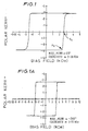
- H n and H c are shown in Figure 1.
- Hc is also large.
- r indicates a square loop and what would fail to be considered square.
- a value of r of under about 0.8 would fail to define a square loop.
- H c are less than or the same order of magnitude as that used as a write-magnetic field, which is typically about 40kA/m.
- write-magnetic fields can change adjacent previously-written information in known Pt/Co multilayers, when writing new information.
- WO 91/08578 discloses a sputtering process for making a platinum/cobalt multilayer film comprised of alternating layers of platinum and cobalt, using as the sputter gas krypton, xenon, or a mixture thereof.
- Multilayer films having a room temperature coercivity of 620-1495 Oe are disclosed and compared with room temperature coercivities 265-360 Oe for multilayer films having the same thickness and number of cobalt and platinum layers, sputtered in argon. It is concluded that the multilayer films sputtered in argon would not be useful for magneto-optical recording.
- Pt/Co multilayer films may therefore be of use in MO applications provided a sufficient room temperature coercivity is achieved whilst also maintaining the other properties described above.
- Mattox Thin Solid Films, 124 (1985) 3-10) discusses how surface preparation is an integral part of any thin film deposition process and outlines the problems to be considered and some general approaches to surface preparation technology.
- U.S. 4,361,472 discloses a method and apparatus for sputtering an element with a magnetron plasma source where a plasma is formed between two electrostatic field defining surfaces of the source and a generator anode disposed adjacent the plasma ejects it toward the element to be sputtered.
- a sputtered Pt/Co multilayer film materials system having a polar Kerr rotation of above 0.1, a square polar Kerr hysteresis loop, and a room temperature coercivity in excess of 2000 Oe, comprising a substrate material; a metal interlayer comprising platinum, of deposited thickness up to 200 ⁇ ; and a Pt/Co multilayer is disclosed.
- the room temperature coercivity of the Pt/Co multilayer film materials system comprising a substrate material; a metal interlayer comprising platinum, of deposited thickness up to 200 ⁇ ; and a Pt/Co multilayer, may be significantly in excess of 2000 Oe, such as in excess of 3000 Oe, or in excess of 4000 Oe, or in excess of 5000 Oe.
- a sputtered Pt/Co multilayer film materials system having a polar Kerr rotation of above 0.1, a square polar Kerr hysteresis loop, and a room temperature coercivity in excess of 1000 Oe, comprising a substrate material; a non-platinum metal interlayer of deposited thickness up to 100 ⁇ ; and a Pt/Co multilayer.
- the non-platinum metal interlayer may comprise a metal selected from the group Pd, Co, Au, Ag, Rh, Ir, and Cu.
- the non-platinum metal interlayer comprises a metal selected from the group Pt, Pd, Co, Au and Ag.
- the platinum or non-platinum metal interlayer preferably has a deposited thickness of up to 50 ⁇ , such as 5-20 ⁇ .
- the substrate material may be any suitable material such as a suitable metal or dielectric material or a polymer such as polycarbonate or glass.
- an "optical enchancement layer" such as silicon nitride
- references to a substrate are intended to include substrates on which are deposited one or more layers of materials for optical enchancment.
- the substrate material may be glass or glass on which is deposited a material selected from the group silicon, silicon nitride and silicon dioxide.
- each cobalt layer preferably has a thickness of up to 12 ⁇ and each platinum layer preferably has a thickness of up to 24 ⁇ .Most preferably, the thickness of each cobalt layer is 2-5 ⁇ and each platinum layer 6-15 ⁇ .
- the multilayer film comprises up to 20 layers in total, or 10 "periods" of Pt/Co, for example 5-10 periods.
- the multilayer films herein desclosed benefit from enchanced coercivity while achieving square polar Kerr hysteresis loops, without the disadvantage which is demonstrated by the prior art metal interlayer MO films in that reading and writing information from the substrate side is prohibited. Coercivities in excess of 5kOe have been achieved using ultra-thin Pt underlayers, 16 ⁇ thick as deposited. In possessing the facility to read and write from the substrate side, the multilayer films of the present invention enjoy a significant advantage over the prior art metal interlayer MO films.
- the multilayer film materials system herein disclosed may be used in any typical magneto-optic disc configuration. Therefore, also disclosed is a magneto-optic disc comprising the multilayer film materials system of the present invention. Typically such a disc would include an optical enhacement layer on the substrate. Optionally, a further optical enchancement layer may be provided on top of the multilayer, and/or a reflective layer of eg Al may be provided.
- the process by which the multilayer films herein disclosed are made is suitable for making not only Pt/Co multilayers, but any metal multilayer.
- the present invention provides an improved process for the manufacture of metal multilayer films which have a metal interlayer and are suitable for magneto-optical recording.
- this invention provides a process for the manufacture of metal multilayer films having perpendicular magnetic anisotropy comprising:
- both the substrate material and the metal interlayer are subject to hyperthermal processing.
- Hyperthermal processing of the metal interlayer may be carried out simultaneously with, or subsequent to, sputter deposition of said interlayer. Said hyperthermal processing will have the effect of reducing the as-deposited thickness of the metal interlayer.
- Sputter deposition may be carried out via any suitable means.
- Many such means such as dc or rf microwave magnetron-, diode-, or triode-sputtering, or sputtering of targets through bombardment by energetic particles from ion or atom guns, are well known in the art.
- the distance between the substrate and the sputter sources of the components of the multilayer may be different, and are variable according to the intitial energy of particles leaving the sputtering target and the nature, pressure, composition and temperature of the sputter gas during sputtering, according to the pressure distance relationship, in order to achieve desirable low arrival energy of condensing metal particles at the substrate during film growth.
- Sputter deposition of the interlayer may be carried out in any noble gas or mixture of noble gases.
- the preferred sputter gases are Ar, Kr and Xe.
- the rate of sputtering may be up to several hundred ⁇ /s of metal but is preferably up to 100 ⁇ /s, eg up to 10 ⁇ /s.
- Hyperthermal processing is used in order to influence the surface characteristics of the substrate and/or metal interlayer, prior to deposition of the interlayer or multilayer.
- the nature of the substrate surface exerts a critical influence on the developing film structure.
- the thin nature of a Pt/Co thin film multilayer permits some degree of control of film growth through surface engineering of growth surfaces to develop aspects of film microstructure beneficial to MO properties.
- the suitably engineered growth surface is not erased by the use of low energy particles in film deposition, and therefore a growth mode providing desirable MO characteristics in the MO film is allowed to be established.
- Hyperthermal processing may conveniently be provided by for example the application of an rf excitation or dc bias to the substrate table, in a low pressure atmosphere, or by placing the substrate or interlayer close to a plasma source, in a low pressure atmosphere, or by particle bombardment from particle guns such as ion or atom guns.
- the applied energy density inducing high energy particle bombardment may conveniently be up to 300Jcm -2 with power densities conveniently up to 0.35Wcm -2 .
- power densities conveniently up to 0.35Wcm -2 .
- greater values of energy density and power density may be used.
- the substrate hyperthermal processing was 140Jcm -2 at 0.33Wcm -2 throughout.
- different values of energy density and power density will give optimum coercivity, for a given substrate and substrate hyperthermal processing regime.
- Sputtering of the metal multilayers may be in any of the noble gases or mixture of noble gases.
- the preferred sputter gases are Ar, Kr and Xe.
- the rate of sputtering may be typically up to 20 ⁇ /s of metal.
- the ability to deposit the multilayer in an argon atmosphere is a substantial economic advantage compared to the prior art recommendations of using xenon or krypton.
- the metal multilayer or the metal interlayer may be thermally treated after deposition.
- the metal multilayer is thermally treated after deposition.
- Said thermal treatment is advantageously carried out in the presence of oxygen, for example in air or in a mixture of gases including air and/or oxygen gas.
- the effect of the thermal treatment is variable according to pressure of oxygen. It may be reasonably expected that the use of pressures above atmosphere may be advantageous. Alternatively, it is thought that said thermal treatment may be carried out in an atmosphere in which oxygen is present as a combined species.
- the thermal treatment comprises the stages of heating, settle, and cool-down although the settle stage is not essential.
- Heating may be up to a temperature of about 200-300°C, such as 200-250°C, and may be at any rate, such as around 10°C/s or around 100°C/s. The rate of heating is not of essential importance.
- the heating may be carried out in one or more stages, with or without the reaching of thermal steady state after each stage. Exposure to heating may be continuous or cycled, or part-continuous and part-cycled.
- Said heating may be provided by any suitable means - for example, heating may be carried out in a furnace, or the sample may be placed in a vessel to be heated, or heating may be provided by one or more than one continuous resistive heat source or lamp source, such as filament or discharge lamp source.
- light bulbs such as halogen light bulbs
- these are placed, with spatial separation from the multilayer film, around, eg above and below, the film. The distance between any bulb and the multilayer film varies, eg according to the wattage of the bulb, the thickness of the film, and the thermal properties of the substrate.
- the bulbs are surrounded by curved reflectors, to intensify and/or make uniform the radiation at the film samples. It is advantageous to use parabolic reflectors to achieve uniform illumination of the sample.
- the second stage of the thermal treatment is the optional settle stage wherein the material is maintained at temperature for a period of time, such as up to 30 minutes, or preferably up to one minute. Thereafter the material is cooled or allowed to cool in one or more stages and if desired at varying rates. Any rate of cooling may be used, such as up to 10°C/s, or preferably up to 100°C/s. Any suitable method of cooling may be employed. If desired, said thermal treatment may be carried out in a magnetic field.
- Figures 1-14 illustrate the MO properties obtained in the multilayer film systems of the corresponding Examples 1-14.
- Examples 1-1C illustrate sputtered Pt/Co multilayer film materials systems having a 16 ⁇ thick Pt interlayer.
- the film of Example 1C is sputtered in xenon.
- Examples 2 and 2A illustrate sputtered Pt/Co multilayer films with 8 ⁇ and 50 ⁇ thick Pt interlayers.
- Example 3 uses interlayers of Pt, Pd, Co. Au and Ag. Cu.
- Examples 4 and 4A employ silicon and silicon nitride "substrates", ie the interlayer is sputtered onto silicon or silicon nitride, but the true substrate would be silicon or silicon nitride on, say, glass.
- Example 5 varies the ratio of Pt/Co in the multilayer and the stack height of the multilayer.
- Examples 6A-D illustrate the effects of hyperthermal processing.
- Examples 7A-F investigate the response of the metal multilayer to thermal treatment.
- Examples 8A-L investigate the relationship between hyperthermal processing and thermal treatment of the interlayer.
- Examples 9-12 compare films subject to various types of thermal treatment as compared with films not so treated.
- Example 13 investigates the effect of atmosphere on the effect of thermal treatment.
- Example 14 illustrates a Pd/Co system
- Example 15 illustrates Pd/Co systems having different interlayers.
- Magneto-optic measurements were performed at 670nm using a custom-built polar Kerr loop tracer. Unless otherwise indicated, measurements were made through the multilayer side of the materials.
- the sputtering machine used was a modified Nordiko NS3750, supplied by Nordiko Ltd of Havant, Hampshire, UK, and modified at the Johnson Matthey Technology Centre.
- the sputtering electrodes in all cases were dc and/or rf planar magnetrons. Unless otherwise stated, all heat treatments were carried out in air, at atmospheric pressure.
- a pre-cleaned glass substrate was mounted onto a substrate table in a vacuum chamber, and the chamber pumped to a base pressure of 2.5 x 10 -6 mb.
- the octagonally-faced substrate table of total surface area 2960cm 2 was situated 11cm from a platinum sputter source and 11cm from a cobalt sputter source and rotated at 6rpm, whilst 1000 watts of constant radio frequency (rf) power at 13.56MHz, equivalent to 0.34Wcm -2 was applied to the table for 7 minutes establishing the table at a negative bias of approximately 245V with respect to ground potential ("Hyperthermal Treatment S1").
- the Pt interlayer was then deposited in two sequential passes by the Pt sputter source, establishing a total thickness of 16 ⁇ .
- the power supplied to the sputter electrode was 124W, the electrode bias was -414V with respect to ground potential.
- the substrate was at a negative potential of 12 to 15V with respect to ground potential.
- the substrate to target separation was 11cm and the table was rotated at 6rpm ("Interlayer Deposition").
- the surface of the Pt interlayer was then hyperthermally treated by applying rf power (13.56MHz) to the substrate table. 200W of rf power was applied for a period of 5 minutes, establishing a table bias with respect to ground of -105V, the substrate table rotating at 6rpm ("Hyperthermal Treatment S2").
- the source of Co flux for the production of the desired multilayer structure was provided by a rf planar magnetron source located directly opposite but facing the Pt source.
- the flux from either source was obscured by the substrate table positioned between them.
- a thin cobalt target was used (8" x 4" x 1mm) to enhance the magnetron sputtering effect.
- power was applied to each source at the values required for the respective deposition rates of Pt or Co respectively, for fabrication of the multilayer structure. This situation was maintained for several minutes enabling equilibration of the sputter sources at the respective power settings for the required deposition rates ("Target Pre-Conditioning Prior to Multilayer Deposition").
- the shuttering obscuring the substrate table was removed such that the flux from both sources was incident at the table, and the substrates rotated past the sources producing an alternating structure of Pt and Co layers.
- the first and last layers being Pt, a structure of 19 layers in total in 9.5 table rotations, was achieved.
- the table rotation was 6rpm, and constant rf power applied to the cobalt sputter electrode to achieve a deposition of approximately 3 ⁇ thick Co layer per substrate pass.
- Constant dc power applied to the Pt sputter electrode achieved approximately an 8 ⁇ thick Pt layer per pass.
- Multilayer Deposition 124W of dc power was applied to the Pt sputter electrode, establishing a bias of -414V on the Pt target.
- the glass substrate with the deposited multilayer was removed from the sputtering chamber.
- the dc power supplied to the electrode was 120W at -414V with respect to ground potential.
- the substrate was an optical disc glass substrate, manufactured by Pilkington Micronics, Clwyd.
- Figure 1B The polar Kerr hysteresis loop obtained is shown in Figure 1B.
- Figure 1B(i) gives the loop obtained through the substrate side of the material.
- the substrate was a glass microscope slide.
- Figure 1C The polar Kerr hysteresis loop obtained is shown in Figure 1C.
- Figure 1C(i) gives the loop obtained through the substrate side of the material.
- the dc power supplied to the electrode was 120W at 414V with respect to ground potential.
- An interlayer of total thickness of approximately 8 ⁇ was established in one deposition pass by the Pt sputter electrode.
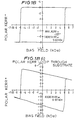
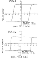
- Figure 2 shows the polar Kerr hysteresis loop obtained.
- the octagonally-faced substrate table of total surface area 2960cm -2 was situated 11cm from the platinum sputter source and 11cm from the cobalt sputter source and rotated at 6rpm, whilst 700watts of constant rf power at 13.56MHz was applied for 20 minutes to the table, equivalent to 0.24Wcm -2 , established the table at a negative bias of approximately 210V with respect to ground potential ("Hyperthermal Treatment S1").
- the Pt interlayer was then deposited by 6 sequential passes by the Pt sputter source, establishing a total thickness of approximately 50 ⁇ .
- the power supplied to the sputter electrode was 120W, the electrode bias was -408V with respect to ground potential.
- the substrate was at a negative potential of 12 to 15V with respect to ground potential.
- the substrate to target separation was 11cm and the table was rotated at 6rpm.
- the surface of the Pt interlayer was then hyperthermally treated by applying rf power (13.56MHz) to the substrate table.
- rf power 13.56MHz
- 150W of rf power was applied for a period of 10 minutes, establishing a table bias with respect to ground of -90V, the substrate table rotating at 6rpm.
- the source of Co flux for the production of the desired multilayer structure was provided by a rf planar magnetron source located directly opposite but facing the dc planar magnetron Pt sputter source.
- the flux from either source was obscured by the substrate table positioned between them.
- a thin cobalt target was used (8" x 4" x 1mm) to enhance the magnetron sputtering effect.
- power was applied to each source at the values required for the respective deposition rates of Pt or Co respectively, for fabrication of the multilayer structure. This situation was maintained for several minutes enabling equilibration of the sputter sources at the respective power settings for the required deposition rates ("Target Pre-conditioning Prior to Multilayer Deposition").
- the shuttering obscuring the substrate table was removed such that the flux from both sources was incident at the table, and the substrates rotated past the sources producing an alternating structuring of Pt and Co layers.
- the first and last layers being Pt, a structure of 19 layers in total in 9.5 table rotations, was achieved.
- the table rotation was 6rpm, and constant rf power applied to the cobalt sputter electrode to achieve a deposition of approximately 3 ⁇ thick Co layer per substrate pass.
- Constant dc power applied to the Pt sputter electrode achieved approximately an 8 ⁇ thick Pt payer per pass. (Multilayer Deposition"). 120W of dc power was applied to the Pt sputter electrode, establishing a bias of -391V on the Pt target.
- the glass substrate with the deposited multilayer was removed from the sputtering chamber.
- MO properties obtained were as follows: "AS-DEPOSITED” SYSTEMS (ie without any thermal treatment) Interlayer Pt Pd Co Ag Au H c (kOe) 2.57 1.56 1.38 1.67 1.89 ⁇ k (°) .23 .22 .3 .13 .17
- the samples having Pt and Pd interlayers were placed in a furnace at 155°C for 40 minutes, in an atmosphere of air and at atmospheric pressure. The samples were then removed from the furnace, placed on an Al block. After 2 minutes the temperature of the samples had fallen to room temperature.
- a silicon nitride "substrate" was mounted into the vacuum chamber and the chamber evacuated.
- the dc power supplied to the electrode was 120W at -406V with respect to ground potential.
- the polar Kerr loop is shown in Figure 4.
- a silicon "substrate” was mounted into the vacuum chamber and the chamber evacuated.
- the structure comprised 15 layers in total in 7.5 table rotations. Approximately 3 ⁇ of Co and 15 ⁇ of Pt were deposited on each pass by each respective electrode. 215W of dc power was applied to the dc electrode establishing a bias of -422V on the Pt sputtering target. 400W of rf power was used to establish self-bias of -570V with respect to ground potential on the Co target. The substrate was at a negative potential of 1 to 2V during multilayer deposition.
- Figure 5 shows the polar Kerr loop obtained.
- the dc power supplied to the electrode was 120W at 409V with regard to ground potential.
- Example 6A-6D were subjected to hyperthermal treatment as follows: 6A No hyperthermal treatment 6B Hyperthermal treatment of substrate only 6C Hyperthermal treatment of interlayer only 6D Hyperthermal treatment of both the substrate and the interlayer.
- the dc power supplied to the electrode was 120W at -374V with regard to ground potnetial whilst 1000W of rf power was applied to the substrate table.
- the substrate table was at a bias of approximately -235V with regard to ground potential during deposition.
- the table rotating at 6rpm and making six deposition passes by the Pt dc magnetron sputter electrode. In the absence of rf biasing of the substrate table the total as-deposited Pt interlayer thickness would be approximately 50 ⁇ .
- Sample 7E was attached to a platinum bar and heated from 23°C to 153°C in 11 ⁇ 2 minutes. The sample was maintained at temperature for 30 minutes and then cooled to 23°C in 4 minutes.
- Sample 7F was attached to a platinum bar, and heated from 24°C to 126°C in one minute. The sample was left at 126°C for 301 ⁇ 2 minutes, after which it was cooled to 24°C in 3 minutes.
- Samples were placed in a furnace at 180°C for 50 minutes. They were then removed and placed in Al block to cool. Room temperature was reached in approximately 2 minutes.
- Samples were placed in a furnace at 155°C for 40 minutes, after which they were taken out, placed in a large Al block. Room temperature was reached in approximately 2 minutes.
- a Pt interlayer approximately 50 ⁇ thick was deposited as in Example 1A except 6 sequential deposition passes were used.
- the argon gas pressure remained at 1.5 x 10 -2 mb throughout all processing stages.
- the substrate was removed from the chamber and thermally treated according to the following process.
- the sample was heated in two cycles.
- the sample was attached to an Al block and heated stepwise from 17°C to 51°C to 100°C to 146°C to 176°C approximately using halogen light bulbs which heated the block.
- the sample was maintained at each intermediate temperature for approximately 3 minutes.
- the temperature of the sample was maintained at 176°C for 15 minutes after which the sample was allowed to cool to room temperature.
- the sample was attached to an Al block and heated stepwise from 18°C to 50°C to 98°C to 146°C to 182°C approximately using halogen light bulbs which heated the block.
- the sample was maintained at each intermediate temperature for approximately 3 minutes.
- the temperature of the sample was maintained at 182°C for 14 minutes after which the sample was allowed to cool to room temperature.
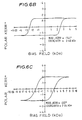
- Figures 9A (i) and 9A (ii) show the polar Kerr loop for the as-deposited and thermally-treated sample, measured through the magneto-optic film.
- the substrate was Pilkington optical data storage disc glass.
- the substrate was removed from the chamber and thermally treated according to the following process.
- the sample was placed in a furnace at 140°C for 60 minutes; then removed from the furnace and allowed to cool to room temperature.
- Figure 9B (i) and 9B (ii) show the polar Kerr loop for the as-deposited and thermally-treated sample measured through the magneto-optic film.
- the substrate was a glass microscope slide.
- the substrate was removed from the chamber and thermally treated according to the following four-stage process.
- the sample was placed in a furnace at 140°C for 60 minutes, removed, and allowed to cool to room temperature.
- the sample was placed first in a furnace at 140°C for 81 minutes, then in the furnace for 64 minutes, and finally in the furnace for 64 minutes. In between each furnace stage and after the last furnace stage, the sample was allowed to cool to room temperature.
- the sample was given four heat treatments in a furnace at 140°C: firstly for 64 minutes. then for 81 minutes, 60 minutes and 169 minutes. As before, in between each furnace stage, and after the final furnace stage, the sample was allowed to cool to room temperature.
- Figures 9C (i) - (v) show polar Kerr loops for the as-deposited sample and after the sample was subjected to successive heat treatments as described above. The sample was measured through the magneto-optic film.
- the substrate was a Pilkington optical data storage disc glass.
- the dc power supplied to the electrode was 120W at -406V with regard to ground potential.
- the sample was heated in air at atmospheric pressure using two 250W halogen light bulbs, (Osram Ltd catalogue number 250-075); half the bulb envelope was gold plated. The distance from the sample surface to the bulb filaments was approximately 38mm.
- the bulbs were switched on for 38 seconds and then cycled for 18 seconds, at a frequency of 1.43Hz with a pulse duration of 0.21 seconds.
- the samples were then placed on an Al block, after 2 minutes the temperature of the sample had fallen to room temperature.
- Figures 10A (i) and 10A (ii) show the polar Kerr rotation at room temperature square loop coercivity before and after thermal treatment for the sample described above.
- Example 10A The sample was heated as in Example 10A with the exception that the bulbs were switched on for 32 seconds and then cycled for 40 seconds in manner described in Example 10A.
- Figures 10B (i) and 10B (ii) show the polar Kerr rotation and room temperature square loop coercivity before and after thermal treatment for the sample described above.
- the substrate was a glass microscope slide.
- Example 10A The sample was heated as in Example 10A with the exception that the bulbs were switched on for 35 seconds and then cycled for 45 seconds in the manner described in Example 10A.
- Figures 10C (i) to 10C (iii) show the polar Kerr rotation and room temperature square loop coercivity and nucleation field before and after thermal treatment processing and showing also through the substrate optical interrogation for the sample described above.
- the sample was placed in a furnace at 153°C for 40 minutes, then removed from the furnace and placed on an Al block; after 2 minutes the sample temperature had fallen to room temperature.
- Figures 11 (a) and (b) shows the polar Kerr rotation and room temperature square loop coercivity and nucleation field before thermal processing and after thermal processing for the sample described above.
- the substrate was SiO 2 for Example 12A and Si in Example 12B.
- the substrate was Si 3 N 4 in Examples 12C and E, and Si in Example 12D.
- the dc power supplied to the electrode was 120W at -406V with regard to ground potential.
- Examples 12A-E were post-deposition heat treated according to the following procedure:
- the sample was heated using one 300W halogen light bulb, similar to those in Example 10A, except the bulb envelope was not gold plated.
- the distance from the sample surface to the bulb filament was approximately 20mm.
- the bulbs were switched on for 30 seconds and then cycled for 60 seconds at a frequency of 1.43Hz and a pulse duration of 0.21 seconds.
- the bulb was then switched off and after 20 minutes the sample was removed from under the bulb and cooled to room temperature in water.
- the sample was attached to an Al block and heated stepwise from 23°C to 85°C to 116°C to 151°C to 180°C approximately using halogen light bulbs which heated the block.
- the sample was maintained at each intermediate temperature for approximately 3 minutes.
- the sample was maintained at 180°C for 33 minutes after which it was allowed to cool to room temperature.
- Example 10A The sample was heated as in Example 10A with the following exceptions: the distance from the sample surface to the bulb filaments was 35mm, and the bulbs were switched on for 90 seconds and then cycled for 60 seconds at a frequency of 1.43Hz with a pulse duration of 0.72 seconds.
- the sample was treated as in Example 12D.
- Table 12 shows the room temperature nucleation field, coercivity and Kerr rotations derived from polar Kerr loop traces for the samples described above before and after thermal treatments.
- Thermally treated 12A 2.1 1.97 0.11 12B 2.04 1.94 0.09 12C 4.79 4.54 0.18 12D 4.84 4.69 0.14 12E 4.39 4.23 0.18
- Example 1A The procedure of Example 1A was followed for the preparation of the multilayer structures.
- a pre-cleaned glass substrate was mounted onto a substrate table in the vacuum chamber, and the chamber pumped to a base pressure of 2.7 x 10 -6 mb.
- the octagonally-faced substrate table of total surface area 2960cm 2 was situated 11cm from the palladium sputter source and 11cm form the cobalt sputter source and rotated at 6rpm, whilst 1000 watts of constant rf power at 13.56MHz was applied for 7 minutes to the table, equivalent to 0.34Wcm -2 , established the table at a negative bias of approximately 265V with respect to ground potential. ("Hyperthermal Treatment S1").
- the Pd interlayer was then deposited by five sequential passes by the Pd sputter source, establishing a total thickness of approximately 50 ⁇ ,
- the power supplied to the sputter electrode was 155W
- the electrode bias was -353V with regard to ground potential.
- the substrate was at a negative potential of 15 to 18V with regard to ground potential.
- the substrate to target separation was 11cm and the table was rotated at 6rpm ("Pd Interlayer Deposition").
- the surface of the Pd interlayer was then hyperthermally treated by applying rf power (13.56MHz) to the substrate table. 200W of rf power was applied for a period of 5 minutes, establishing a table bias with regard to ground potential of -110V, the substrate table rotating at 6rpm ("Hyperthermal Treatment S2").
- the Ar gas pressure was adjusted to 2.5x10 -2 mb.
- the source of Co flux for the production of the desired multilayer structure was provided by a rf planar magnetron source located directly opposite but facing a dc planar magnetron Pd source.
- the flux from either source was obscured by the substrate table positioned between them.
- a thin cobalt target was used (8" x 4" x 1mm) to enhance the magnetron sputtering effect.
- power was applied to each source at the value required for the respective deposition rates of Pd or Co respectively, for fabrication of the multilayer structure. This situation was maintained for several minutes enabling equilibration of the sputter sources at the respective power settings for the required deposition rates ("Target Pre-conditioning Prior to Multilayer Deposition").
- the shuttering obscuring the substrate table was removed such that the flux from both sources was incident at the table, and the substrates rotated past the sources producing an alternating structure of Pd and Co layers.
- the first and last layers being Pd, a structure of 17 layers in total in 8.5 table rotations, was achieved.
- the table rotation was 6rpm, and constant rf power applied to the cobalt sputter electrode to achieve a deposition of approximately 3 ⁇ thick Co layer per substrate pass.
- Constant dc power applied to the Pd sputter electrode achieved approximately a 9 ⁇ thick Pd layer per pass.
- 140W of dc power was applied to the Pd sputter electrode, establishing a bias of -320V on the Pd target.
- 400W of rf power was used to establish a self-bias of -570V with regard to ground potential on the Co target.
- the substrate was at a negative potential of 5V with respect to ground potential.
- the glass substrate with the deposited multilayer was removed from the sputtering chamber.
- the polar Kerr loop for this sample is shown in Figure 14.
- the sample having the Pt interlayer was attached to an Al block which was then heated by halogen light bulbs.
- the sample was heated in stepwise manner, from 19°C to 83°C to 120°C to 150°C. After each step the sample was allowed to settle for 3 minutes; after the final heat step it was allowed to settle for 13 minutes. The sample was then cooled, using forced air cooling, to 22°C in 12 minutes.
- H c and ⁇ k were as follows: H c (kOe) 3.27 ⁇ k (°) 0.05
Landscapes
- Engineering & Computer Science (AREA)
- Chemical & Material Sciences (AREA)
- Nanotechnology (AREA)
- Crystallography & Structural Chemistry (AREA)
- Power Engineering (AREA)
- Manufacturing & Machinery (AREA)
- Metallurgy (AREA)
- Organic Chemistry (AREA)
- Mechanical Engineering (AREA)
- Materials Engineering (AREA)
- Chemical Kinetics & Catalysis (AREA)
- Physics & Mathematics (AREA)
- Condensed Matter Physics & Semiconductors (AREA)
- Spectroscopy & Molecular Physics (AREA)
- General Physics & Mathematics (AREA)
- Physical Vapour Deposition (AREA)
- Thin Magnetic Films (AREA)
- Laminated Bodies (AREA)
- Extrusion Moulding Of Plastics Or The Like (AREA)
- Optical Record Carriers And Manufacture Thereof (AREA)
Abstract
Description
- This invention relates to a novel platinum/cobalt multilayer film materials system and to an improved process for the manufacture of metal multilayer films.
- Thin films with perpendicular magnetic anisotropy are potential candidates in high density magnetic and magneto-optical (MO) recording. Amorphous rare earth transition metal alloy films have become the dominant MO recording media. However, there are a number of major disadvantages associated with these films, eg they suffer from poor corrosion resistance and easy oxidation, necessitating the use of passivating underlayers and overcoats, and small Kerr rotation at short wavelengths, preventing their use for high density recording with shorter wavelength or "blue" lasers. Pt/Co and Pd/Co multilayers have been proposed as MO media candidates. Pt/Co multilayers are preferred because they exhibit a higher polar Kerr effect than Pd/Co multilayers, particularly at shorter wavelengths.
- In order to be potentially useful for magneto-optical recording, a material must have, in addition to perpendicular magnetic anisotropy, a square polar Kerr hysteresis loop, a sufficient polar Kerr rotation (k), and a sufficiently large room temperature coercivity (Hc). An unenhanced polar Kerr rotation of around 0.1° would be regarded as sufficient for MO purposes, although higher values, say around 0.2-0.3°, would be preferred. There are known ways of enhancing polar Kerr rotation. Coercivity plays a key role in thermomagnetic recording, and should be larger at room temperature than the field applied during writing. Otherwise, write-magnetic fields can change adjacent previously-written information in a multilayer. In general, coercivities of about 1000 Oe (80kA/m) are sufficiently high. However, high coercivity alone is not enough to make a multilayer film suitable for magneto-optical recording. A square polar Kerr hysteresis loop is also required. Such a loop is defined by W B Zeper et al in "Hysteresis, microstructure, and magneto-optical recording in Co/Pt and Co/Pd multilayers", J. Appl. Phys., 70 (4), 15 August 1991, where the "squareness" of the loop is defined as the rectangular ratio r=Hn/Hc, where r is the rectangular ratio, Hn is the nucleation field and Hc is the coercive field. Hn and Hc are shown in Figure 1. For a magneto-optical recording medium r=1 is the optimum where the Hc is also large. However, to our knowledge there is no widely accepted definition of what value of r indicates a square loop and what would fail to be considered square. We would suggest that a value of r of under about 0.8 would fail to define a square loop.
- The best MO recording performances are achieved in Pt/Co multilayers which are deposited by evaporation or molecular beam techniques. Although sputtering techniques are preferred over these techniques, because of its ease of use in large scale manufacture, sputtered films generally have insufficient coercivity at room temperature to be of use in magneto-optic recording. For example, Ochiai et al, Jap J Appl Phys 28, L659 (1989) and Ochiai et al, Digest of the Int'l Mag Conf 1989 Wash, DC report Hc of only 100-350 Oe (8-28 kA/m) for sputtered Pt/Co multilayers which they prepared by using argon as the sputter gas. These values of Hc are less than or the same order of magnitude as that used as a write-magnetic field, which is typically about 40kA/m. As a result, write-magnetic fields can change adjacent previously-written information in known Pt/Co multilayers, when writing new information.
- WO 91/08578 discloses a sputtering process for making a platinum/cobalt multilayer film comprised of alternating layers of platinum and cobalt, using as the sputter gas krypton, xenon, or a mixture thereof. Multilayer films having a room temperature coercivity of 620-1495 Oe are disclosed and compared with room temperature coercivities 265-360 Oe for multilayer films having the same thickness and number of cobalt and platinum layers, sputtered in argon. It is concluded that the multilayer films sputtered in argon would not be useful for magneto-optical recording.
- Pt/Co multilayer films may therefore be of use in MO applications provided a sufficient room temperature coercivity is achieved whilst also maintaining the other properties described above. Various attempts have been made to improve Hc, such as the use of underlayers.
- For example, Y Ochiai et al, EP 0304873 disclose studies of sputtered Pt/Co multilayers including the use of underlayers to increase Hc. However, generally only marginal improvements in Hc were achieved and the singular best result of 700 Oe (56kA/m) requires 1000Å (100nm) thick Pt underlayer. This is impractical for most magneto-optical recording applications because it prohibits reading and writing information from the substrate side and the relatively large heat capacity and thermal diffusivity of such a thick Pt layer will likely inhibit writing with the limited power available with current solid-state lasers.
- Underlayers of zinc oxide or indium oxide, thickness about 200 to about 4500Å, are enclosed in WO 91/14263. Room temperature coercivities of 1090-2900 Oe are achieved. A complicated process wherein the oxide layer has to be sputtered in the presence of oxygen, while the multilayer is sputtered in a separate vacuum chamber. Transfer from one chamber to the other exposes the zinc oxide film to the atmosphere and an additional process step is required to remove any contamination occurring during exposure.
- Mattox (Thin Solid Films, 124 (1985) 3-10) discusses how surface preparation is an integral part of any thin film deposition process and outlines the problems to be considered and some general approaches to surface preparation technology.
- U.S. 4,361,472 discloses a method and apparatus for sputtering an element with a magnetron plasma source where a plasma is formed between two electrostatic field defining surfaces of the source and a generator anode disposed adjacent the plasma ejects it toward the element to be sputtered.
- Other work has involved heating of growth surfaces, or substrates, to improve the properties of the deposited film.
- We now disclose a sputtered, Pt/Co multilayer film materials system having superior room temperature coercivity, a square polar Kerr hysteresis loop, and sufficient Polar Kerr rotation, which may be used as a magneto-optical recording medium.
- Accordingly, a sputtered Pt/Co multilayer film materials system having a polar Kerr rotation of above 0.1, a square polar Kerr hysteresis loop, and a room temperature coercivity in excess of 2000 Oe, comprising a substrate material; a metal interlayer comprising platinum, of deposited thickness up to 200Å; and a Pt/Co multilayer is disclosed.
- The room temperature coercivity of the Pt/Co multilayer film materials system comprising a substrate material; a metal interlayer comprising platinum, of deposited thickness up to 200Å; and a Pt/Co multilayer, may be significantly in excess of 2000 Oe, such as in excess of 3000 Oe, or in excess of 4000 Oe, or in excess of 5000 Oe.
- Also disclosed is a sputtered Pt/Co multilayer film materials system having a polar Kerr rotation of above 0.1, a square polar Kerr hysteresis loop, and a room temperature coercivity in excess of 1000 Oe, comprising a substrate material; a non-platinum metal interlayer of deposited thickness up to 100Å; and a Pt/Co multilayer.
- The non-platinum metal interlayer may comprise a metal selected from the group Pd, Co, Au, Ag, Rh, Ir, and Cu. Preferably the non-platinum metal interlayer comprises a metal selected from the group Pt, Pd, Co, Au and Ag.
- For ease of reading and writing information from the substrate side, thinner interlayers are much preferred. Therefore, the platinum or non-platinum metal interlayer preferably has a deposited thickness of up to 50Å, such as 5-20Å.
- The substrate material may be any suitable material such as a suitable metal or dielectric material or a polymer such as polycarbonate or glass. In a commercial MO disc it is common practice to include an "optical enchancement layer", such as silicon nitride, between the substrate and the MO material. For the purposes of this application, therefore, references to a substrate are intended to include substrates on which are deposited one or more layers of materials for optical enchancment. For example, therefore, the substrate material may be glass or glass on which is deposited a material selected from the group silicon, silicon nitride and silicon dioxide.
- In the multilayer, each cobalt layer preferably has a thickness of up to 12Å and each platinum layer preferably has a thickness of up to 24Å.Most preferably, the thickness of each cobalt layer is 2-5Å and each platinum layer 6-15Å. Preferably, the multilayer film comprises up to 20 layers in total, or 10 "periods" of Pt/Co, for example 5-10 periods.
- The multilayer films herein desclosed benefit from enchanced coercivity while achieving square polar Kerr hysteresis loops, without the disadvantage which is demonstrated by the prior art metal interlayer MO films in that reading and writing information from the substrate side is prohibited. Coercivities in excess of 5kOe have been achieved using ultra-thin Pt underlayers, 16Å thick as deposited. In possessing the facility to read and write from the substrate side, the multilayer films of the present invention enjoy a significant advantage over the prior art metal interlayer MO films.
- The multilayer film materials system herein disclosed may be used in any typical magneto-optic disc configuration. Therefore, also disclosed is a magneto-optic disc comprising the multilayer film materials system of the present invention. Typically such a disc would include an optical enhacement layer on the substrate. Optionally, a further optical enchancement layer may be provided on top of the multilayer, and/or a reflective layer of eg Al may be provided.
- The process by which the multilayer films herein disclosed are made is suitable for making not only Pt/Co multilayers, but any metal multilayer.
- Therefore, the present invention provides an improved process for the manufacture of metal multilayer films which have a metal interlayer and are suitable for magneto-optical recording.
- Accordingly, this invention provides a process for the manufacture of metal multilayer films having perpendicular magnetic anisotropy comprising:
- i) sputter depositing onto a substrate material a metal interlayer of as deposited thickness up to 200Å, and
- ii) sputter depositing onto the interlayer a metal multilayer, characterised in that at least one of the substrate and the metal interlayer is subjected to hyperthermal processing comprising the application of an rf excitation or dc bias to the substrate table in a low pressure atmosphere, or by placing the substrate or interlayer close to a plasma source in a low pressure atmosphere, or by particle bombardment from particle guns such as ion or atom guns, wherein the hyperthermal processing influences the surface characteristics of the substrate and/or interlayer prior to deposition of the interlayer or multilayer, and wherein hyperthermal processing of the interlayer, if present, is carried out simultaneously with, or subsequent to, deposition of the interlayer.
-
- Preferably, both the substrate material and the metal interlayer are subject to hyperthermal processing.
- Hyperthermal processing of the metal interlayer may be carried out simultaneously with, or subsequent to, sputter deposition of said interlayer. Said hyperthermal processing will have the effect of reducing the as-deposited thickness of the metal interlayer.
- Sputter deposition may be carried out via any suitable means. Many such means, such as dc or rf microwave magnetron-, diode-, or triode-sputtering, or sputtering of targets through bombardment by energetic particles from ion or atom guns, are well known in the art.
- During multilayer sputtering, the distance between the substrate and the sputter sources of the components of the multilayer may be different, and are variable according to the intitial energy of particles leaving the sputtering target and the nature, pressure, composition and temperature of the sputter gas during sputtering, according to the pressure distance relationship, in order to achieve desirable low arrival energy of condensing metal particles at the substrate during film growth.
- Sputter deposition of the interlayer may be carried out in any noble gas or mixture of noble gases. The preferred sputter gases are Ar, Kr and Xe. The rate of sputtering may be up to several hundred Å/s of metal but is preferably up to 100Å/s, eg up to 10Å/s.
- Hyperthermal processing is used in order to influence the surface characteristics of the substrate and/or metal interlayer, prior to deposition of the interlayer or multilayer. In the initial stages of film growth, the nature of the substrate surface exerts a critical influence on the developing film structure. The thin nature of a Pt/Co thin film multilayer permits some degree of control of film growth through surface engineering of growth surfaces to develop aspects of film microstructure beneficial to MO properties. In the process of the present invention there is no need to apply heat in order to advantageously enhance MO properties. The suitably engineered growth surface is not erased by the use of low energy particles in film deposition, and therefore a growth mode providing desirable MO characteristics in the MO film is allowed to be established.
- Hyperthermal processing may conveniently be provided by for example the application of an rf excitation or dc bias to the substrate table, in a low pressure atmosphere, or by placing the substrate or interlayer close to a plasma source, in a low pressure atmosphere, or by particle bombardment from particle guns such as ion or atom guns.
- Where rf excitation is employed in hyperthermal processing performed on the substrate, where interlayers of as-deposited thicknesses of up to approximately 50Å are to be applied, the applied energy density inducing high energy particle bombardment may conveniently be up to 300Jcm-2 with power densities conveniently up to 0.35Wcm-2. However, depending on the nature of the substrate greater values of energy density and power density may be used.
- In a specific example, where rf excitation is employed in hyperthermal treatment of the interlayer, for approximately 16Å and 25Å as-deposited Pt interlayer thicknesses on a glass microscope slide, no significant benefit is obtained for energy densities in excess of 100Jcm-2 and power densities in excess of 0.3Wcm-2. Optimum values of coercivity are obtained in interlayer hyperthermal processing having values of approximately 20Jcm-2 and 0.067Wcm-2 for 16Å thick Pt interlayers. For the 25Å thick Pt interlayers optimum coercivity is observed with the interlayer hyperthermal processing at approximately 40Jcm-2 and 0.133Wcm-2. The substrate hyperthermal processing was 140Jcm-2 at 0.33Wcm-2 throughout. For different metal interlayers and different as-deposited interlayer thicknesses, different values of energy density and power density will give optimum coercivity, for a given substrate and substrate hyperthermal processing regime.
- Sputtering of the metal multilayers may be in any of the noble gases or mixture of noble gases. The preferred sputter gases are Ar, Kr and Xe. The rate of sputtering may be typically up to 20Å/s of metal.
- The ability to deposit the multilayer in an argon atmosphere is a substantial economic advantage compared to the prior art recommendations of using xenon or krypton.
- The metal multilayer or the metal interlayer may be thermally treated after deposition. Preferably the metal multilayer is thermally treated after deposition. Said thermal treatment is advantageously carried out in the presence of oxygen, for example in air or in a mixture of gases including air and/or oxygen gas. The effect of the thermal treatment is variable according to pressure of oxygen. It may be reasonably expected that the use of pressures above atmosphere may be advantageous. Alternatively, it is thought that said thermal treatment may be carried out in an atmosphere in which oxygen is present as a combined species.
- In general the thermal treatment comprises the stages of heating, settle, and cool-down although the settle stage is not essential. Heating may be up to a temperature of about 200-300°C, such as 200-250°C, and may be at any rate, such as around 10°C/s or around 100°C/s. The rate of heating is not of essential importance. The heating may be carried out in one or more stages, with or without the reaching of thermal steady state after each stage. Exposure to heating may be continuous or cycled, or part-continuous and part-cycled. Said heating may be provided by any suitable means - for example, heating may be carried out in a furnace, or the sample may be placed in a vessel to be heated, or heating may be provided by one or more than one continuous resistive heat source or lamp source, such as filament or discharge lamp source. Accordingly, light bulbs, such as halogen light bulbs, may be employed as the heating source in the present invention. Where light bulbs are employed, one or more may be used. In the method of the invention these are placed, with spatial separation from the multilayer film, around, eg above and below, the film. The distance between any bulb and the multilayer film varies, eg according to the wattage of the bulb, the thickness of the film, and the thermal properties of the substrate. Advantageously, the bulbs are surrounded by curved reflectors, to intensify and/or make uniform the radiation at the film samples. It is advantageous to use parabolic reflectors to achieve uniform illumination of the sample.
- The second stage of the thermal treatment is the optional settle stage wherein the material is maintained at temperature for a period of time, such as up to 30 minutes, or preferably up to one minute. Thereafter the material is cooled or allowed to cool in one or more stages and if desired at varying rates. Any rate of cooling may be used, such as up to 10°C/s, or preferably up to 100°C/s. Any suitable method of cooling may be employed. If desired, said thermal treatment may be carried out in a magnetic field.
- In a commercial environment, rates of heating and cooling would be as high as possible.
- The invention will now be described in the following examples, which are intended to illustrate but not to limit the scope of the invention.
- Figures 1-14 illustrate the MO properties obtained in the multilayer film systems of the corresponding Examples 1-14.
- Examples 1-1C illustrate sputtered Pt/Co multilayer film materials systems having a 16Å thick Pt interlayer. The film of Example 1C is sputtered in xenon.
- Examples 2 and 2A illustrate sputtered Pt/Co multilayer films with 8Å and 50Å thick Pt interlayers.
- Example 3 uses interlayers of Pt, Pd, Co. Au and Ag. Cu.
- Examples 4 and 4A employ silicon and silicon nitride "substrates", ie the interlayer is sputtered onto silicon or silicon nitride, but the true substrate would be silicon or silicon nitride on, say, glass.
- Example 5 varies the ratio of Pt/Co in the multilayer and the stack height of the multilayer.
- Examples 6A-D illustrate the effects of hyperthermal processing.
- Examples 7A-F investigate the response of the metal multilayer to thermal treatment.
- Examples 8A-L investigate the relationship between hyperthermal processing and thermal treatment of the interlayer.
- Examples 9-12 compare films subject to various types of thermal treatment as compared with films not so treated.
- Example 13 investigates the effect of atmosphere on the effect of thermal treatment.
- Example 14 illustrates a Pd/Co system, and Example 15 illustrates Pd/Co systems having different interlayers.
- Magneto-optic measurements were performed at 670nm using a custom-built polar Kerr loop tracer. Unless otherwise indicated, measurements were made through the multilayer side of the materials.
- In all Examples the sputtering machine used was a modified Nordiko NS3750, supplied by Nordiko Ltd of Havant, Hampshire, UK, and modified at the Johnson Matthey Technology Centre. The sputtering electrodes in all cases were dc and/or rf planar magnetrons. Unless otherwise stated, all heat treatments were carried out in air, at atmospheric pressure.
- A pre-cleaned glass substrate was mounted onto a substrate table in a vacuum chamber, and the chamber pumped to a base pressure of 2.5 x 10⁻⁶ mb.
- Pure Ar gas was metered into a pumped chamber to attain a pressure of 1.5 x 10⁻²mb and the system allowed to equilibrate for several minutes. ("
Gas Equilibration 1"). - The octagonally-faced substrate table of total surface area 2960cm2 was situated 11cm from a platinum sputter source and 11cm from a cobalt sputter source and rotated at 6rpm, whilst 1000 watts of constant radio frequency (rf) power at 13.56MHz, equivalent to 0.34Wcm-2 was applied to the table for 7 minutes establishing the table at a negative bias of approximately 245V with respect to ground potential ("Hyperthermal Treatment S1").
- With the substrate table obscured by shutters from a planar magnetron source fitted with an 8" x 4" Pt target, 124W of dc power was applied to the sputter source for several minutes, to clean the sputter target and establish a steady state of operation ("Target Pre-Conditioning Stage").
- The Pt interlayer was then deposited in two sequential passes by the Pt sputter source, establishing a total thickness of 16Å. The power supplied to the sputter electrode was 124W, the electrode bias was -414V with respect to ground potential. The substrate was at a negative potential of 12 to 15V with respect to ground potential. The substrate to target separation was 11cm and the table was rotated at 6rpm ("Interlayer Deposition").
- The surface of the Pt interlayer was then hyperthermally treated by applying rf power (13.56MHz) to the substrate table. 200W of rf power was applied for a period of 5 minutes, establishing a table bias with respect to ground of -105V, the substrate table rotating at 6rpm ("Hyperthermal Treatment S2").
- The source of Co flux for the production of the desired multilayer structure was provided by a rf planar magnetron source located directly opposite but facing the Pt source. The flux from either source was obscured by the substrate table positioned between them. A thin cobalt target was used (8" x 4" x 1mm) to enhance the magnetron sputtering effect. With the substrates obscured from both sputter sources, power was applied to each source at the values required for the respective deposition rates of Pt or Co respectively, for fabrication of the multilayer structure. This situation was maintained for several minutes enabling equilibration of the sputter sources at the respective power settings for the required deposition rates ("Target Pre-Conditioning Prior to Multilayer Deposition").
- The shuttering obscuring the substrate table was removed such that the flux from both sources was incident at the table, and the substrates rotated past the sources producing an alternating structure of Pt and Co layers. The first and last layers being Pt, a structure of 19 layers in total in 9.5 table rotations, was achieved. The table rotation was 6rpm, and constant rf power applied to the cobalt sputter electrode to achieve a deposition of approximately 3Å thick Co layer per substrate pass. Constant dc power applied to the Pt sputter electrode achieved approximately an 8Å thick Pt layer per pass. ("Multilayer Deposition"). 124W of dc power was applied to the Pt sputter electrode, establishing a bias of -414V on the Pt target. 400W of rf power was used to establish a self-bias of -600V with respect to ground on the Cc target. The substrate was at a negative potential of 1 to 2V with respect to ground. The gas metering and separations of the sputter electrodes with respect to the substrate table were as previously described under "Hyperthermal Treatment S1".
- The glass substrate with the deposited multilayer was removed from the sputtering chamber.
- The polar Kerr hysteresis loop for this Example is shown in Figure 1.
- The procedure of Example 1 was followed with the following notable adjustments:
- In the "Target pre-conditioning" stage, 120W of dc power was applied.
- During the "Interlayer Deposition" stage, the dc power supplied to the electrode was 120W at -414V with respect to ground potential.
- After "Hyperthermal Treatment S2", the argon gas pressure was adjusted to 2.5 x 10⁻²mb. ("
Gas Equilibration 2"). - In the "Multilayer Deposition" stage 120W of dc power was applied to the dc electrode establishing a bias of -400V on the Pt sputtering target.
- The polar Kerr hysteresis loop obtained is shown in Figure 1A.
- The procedure of Example 1A was followed with the following notable adjustments:
- The substrate was an optical disc glass substrate, manufactured by Pilkington Micronics, Clwyd.
- During the "
Gas Equilibration 2" stage the argon gas pressure was adjusted to 3.5 x 10⁻²mb - In the "Multilayer Deposition" stage 120W of dc power was applied to the dc electrode establishing a bias of -380V on the Pt sputtering target. 400W of rf power was used to establish self-bias of -570V with respect to ground potential on the Co target.
- The polar Kerr hysteresis loop obtained is shown in Figure 1B. Figure 1B(i) gives the loop obtained through the substrate side of the material.
- The procedure of Example 1A was followed with the following notable adjustments:
- The substrate was a glass microscope slide.
- During the "
Gas Equilibration 2" stage the argon gas was pumped from the chamber and Xe gas admitted such that a pressure of 1.3 x 10⁻²mb was established. - In the "Multilayer Deposition" stage 120W of dc power was applied to the dc electrode establishing a bias of -624V on the Pt sputtering target. 400W of rf power was used to establish self-bias of -550V with respect to ground potential on the Co target. The substrate was at a negative potential of 1-2V with respect to ground potential.
- The polar Kerr hysteresis loop obtained is shown in Figure 1C. Figure 1C(i) gives the loop obtained through the substrate side of the material.
- The procedure of Example 1 was followed with the following notable adjustments:
- In the "Target Pre-conditioning" stage, 120W of dc power was applied.
- During the "Interlayer Deposition" stage the dc power supplied to the electrode was 120W at 414V with respect to ground potential. An interlayer of total thickness of approximately 8Å was established in one deposition pass by the Pt sputter electrode.
- A "
Gas Equilibration 2" stage (see Example 1A) was included, in which the argon gas pressure was adjusted to 2.5 x 10⁻²mb. - In the "Multilayer Deposition" stage 120W of dc power was applied to the dc electrode establishing a bias of -386V on the Pt sputtering target. 400W of rf power was applied to the Co target establishing a self-bias of -386V with respect to ground potential.
- Figure 2 shows the polar Kerr hysteresis loop obtained.
-
Paragraphs - The octagonally-faced substrate table of total surface area 2960cm-2 was situated 11cm from the platinum sputter source and 11cm from the cobalt sputter source and rotated at 6rpm, whilst 700watts of constant rf power at 13.56MHz was applied for 20 minutes to the table, equivalent to 0.24Wcm-2, established the table at a negative bias of approximately 210V with respect to ground potential ("Hyperthermal Treatment S1").
- With the substrate table obscured by shutters from a planar magnetron source fitted with an 8" x 4" Pt target, 120W of dc power was applied to the sputter source for several minutes, to clean the sputter target and establish a steady state of operation ("Target Pre-conditioning Stage").
- The Pt interlayer was then deposited by 6 sequential passes by the Pt sputter source, establishing a total thickness of approximately 50Å. The power supplied to the sputter electrode was 120W, the electrode bias was -408V with respect to ground potential. The substrate was at a negative potential of 12 to 15V with respect to ground potential. The substrate to target separation was 11cm and the table was rotated at 6rpm. ("Interlayer Deposition").
- The surface of the Pt interlayer was then hyperthermally treated by applying rf power (13.56MHz) to the substrate table. 150W of rf power was applied for a period of 10 minutes, establishing a table bias with respect to ground of -90V, the substrate table rotating at 6rpm. ("Hyperthermal Treatment S2").
- The argon gas pressure was then adjusted to 2.5 x 10⁻²mb and allowed to equilibrate. ("
Gas Equilibration 2"). - The source of Co flux for the production of the desired multilayer structure was provided by a rf planar magnetron source located directly opposite but facing the dc planar magnetron Pt sputter source. The flux from either source was obscured by the substrate table positioned between them. A thin cobalt target was used (8" x 4" x 1mm) to enhance the magnetron sputtering effect. With the substrates obscured from both sputter sources, power was applied to each source at the values required for the respective deposition rates of Pt or Co respectively, for fabrication of the multilayer structure. This situation was maintained for several minutes enabling equilibration of the sputter sources at the respective power settings for the required deposition rates ("Target Pre-conditioning Prior to Multilayer Deposition").
- The shuttering obscuring the substrate table was removed such that the flux from both sources was incident at the table, and the substrates rotated past the sources producing an alternating structuring of Pt and Co layers. The first and last layers being Pt, a structure of 19 layers in total in 9.5 table rotations, was achieved. The table rotation was 6rpm, and constant rf power applied to the cobalt sputter electrode to achieve a deposition of approximately 3Å thick Co layer per substrate pass. Constant dc power applied to the Pt sputter electrode achieved approximately an 8Å thick Pt payer per pass. (Multilayer Deposition"). 120W of dc power was applied to the Pt sputter electrode, establishing a bias of -391V on the Pt target. 400W of rf power was used, to establish a self-bias of -560V with respect to ground potential on the Co target. The substrate was at a negative potential of 1 to 2V with respect to ground potential. The gas metering and separations of the sputter electrodes with respect to the substrates tables was as previously described. ("Hyperthermal Treatment S1", "
Gas Equilibration 2"). - The glass substrate with the deposited multilayer was removed from the sputtering chamber.
- The polar Kerr hysteresis loop obtained is shown in Figure 2A.
- The procedure of example 1A was followed with the following notable adjustments:
- In the "Interlayer Deposition" stage approximately 50Å thick Pt or Pd or Co or Ag or Au interlayers were deposited in a manner similar to that described for the Pt interlayer illustrated in previous Examples with suitable adjustment of power applied to the sputtering target, number of target passes and speed of substrate table rotation to achieve an interlayer thickness of 50Å.
- MO properties obtained were as follows:
"AS-DEPOSITED" SYSTEMS (ie without any thermal treatment)Interlayer Pt Pd Co Ag Au Hc (kOe) 2.57 1.56 1.38 1.67 1.89 k (°) .23 .22 .3 .13 .17 - The samples having Pt and Pd interlayers were placed in a furnace at 155°C for 40 minutes, in an atmosphere of air and at atmospheric pressure. The samples were then removed from the furnace, placed on an Al block. After 2 minutes the temperature of the samples had fallen to room temperature.
- The MO properties then measured were as follows:
-
Interlayer Pt Pd Hc (kOe) 3.31 1.82 k (°) .21 .20 - The procedure of Example 1 was followed with the following notable adjustments:
- A silicon nitride "substrate" was mounted into the vacuum chamber and the chamber evacuated.
- In the "Target pre-conditioning" stage, 120W of dc power was applied.
- During the "Interlayer Deposition" stage the dc power supplied to the electrode was 120W at -406V with respect to ground potential.
- During the "
Gas Equilibration 2" stage the argon gas pressure was adjusted to 2.5 x 10⁻²mb - In the "Multilayer Deposition" stage 120W of dc power was applied to the dc electrode establishing a bias of -384V on the Pt sputtering target. 400W of rf power was applied to the Co target, establishing a self-bias of -575V with respect to ground potential on the Co target.
- The polar Kerr loop is shown in Figure 4.
- The procedure of Example 4 was followed with the following notable adjustments:
- A silicon "substrate" was mounted into the vacuum chamber and the chamber evacuated.
- Square loop coercivity is shown in Figure 4A.
- The procedure of Example 1A was followed with the following notable adjustments:
- During the "
Gas Equilibration 2" stage the argon gas pressure was adjusted to 2.5 x 10⁻²mb. - In the "Multilayer Deposition" stage the structure comprised 15 layers in total in 7.5 table rotations. Approximately 3Å of Co and 15Å of Pt were deposited on each pass by each respective electrode. 215W of dc power was applied to the dc electrode establishing a bias of -422V on the Pt sputtering target. 400W of rf power was used to establish self-bias of -570V with respect to ground potential on the Co target. The substrate was at a negative potential of 1 to 2V during multilayer deposition.
- Figure 5 shows the polar Kerr loop obtained.
- The procedure of Example 1A was followed with the following notable adjustments:
- During the "Interlayer Deposition" stage the dc power supplied to the electrode was 120W at 409V with regard to ground potential.
- In the "Multilayer Deposition" stage 120W of dc power was applied to the dc electrode establishing a bias of -386V on the Pt sputtering target. 400W of rf power was applied to the Co planar magnetron sputter electrode establishing a self-bias of -560V with regard to ground potential. The substrate table was at a bias of negative 1-2V with regard to ground potential.
- Each of Examples 6A-6D were subjected to hyperthermal treatment as follows:
6A No hyperthermal treatment 6B Hyperthermal treatment of substrate only 6C Hyperthermal treatment of interlayer only 6D Hyperthermal treatment of both the substrate and the interlayer. - The polar Kerr loops for the above are shown in Figures 6A-6D respectively. Clearly, hyperthermal processing of both the substrate and the interlayer gives the best results.
- The deposition procedure of Example 1A was followed with the following notable adjustments:
- During the "Interlayer Deposition" stage for bias grown interlayers the dc power supplied to the electrode was 120W at -374V with regard to ground potnetial whilst 1000W of rf power was applied to the substrate table. The substrate table was at a bias of approximately -235V with regard to ground potential during deposition. The table rotating at 6rpm and making six deposition passes by the Pt dc magnetron sputter electrode. In the absence of rf biasing of the substrate table the total as-deposited Pt interlayer thickness would be approximately 50Å.
- In the "Multilayer Deposition" stage 120W of dc power was applied to the dc electrode establishing a bias of -386V on the Pt sputtering target. 400W of rf power was applied to the Co planar magnetron sputtering target establishing a self-bias of -560V with regard to ground potential.
- The combinations of bias grown interlayers with hyperthermal processing stages in multilayer fabrication and any subsequent post-deposition thermal treatment for the following Examples are shown in the Table below.
Example S1 S2 Post-Deposition Thermal Treatment 7A * * 7B * - 7C - * 7D - - 7E * * * 7F * - * * = Process applied
- = Process absent - Where applicable post-deposition thermal treatment was carried out according to the following procedure:
- Sample 7E was attached to a platinum bar and heated from 23°C to 153°C in 1½ minutes. The sample was maintained at temperature for 30 minutes and then cooled to 23°C in 4 minutes.
- Sample 7F was attached to a platinum bar, and heated from 24°C to 126°C in one minute. The sample was left at 126°C for 30½ minutes, after which it was cooled to 24°C in 3 minutes.
- The Table below shows the room temperature coercivity and Kerr rotation for the above Examples.
Example Hc (kOe) (°) 7A 5.3 0.29 7B 4.23 0.28 7C 5.92 0.28 7D 3.71 0.24 7E 7.31 0.25 7F 4.86 0.27 - The stages S1 Interlayer Thermal Treatment, S2, Post-Deposition Thermal Treatment, were carried out as indicated below for Examples 8A-8L, following appropriately the procedure of Example 1A.
Example S1 Interlayer Thermal Treatment S2 Post-Deposition Thermal Treatment 8A - - - * 8B * - - * 8C - - * * 8D * - * * 8E - * - - 8F * * - - 8G - * * - 8H * * * - 8I - * - * 8J * * - * 8K - * * * 8L * * * * Note: - = process not applied
* = process applied - S1 and S2 were as previously described; the thermal treatment process for the interlayer and/or multilayer is described below:
- Samples were placed in a furnace at 180°C for 50 minutes. They were then removed and placed in Al block to cool. Room temperature was reached in approximately 2 minutes.
- Samples were placed in a furnace at 155°C for 40 minutes, after which they were taken out, placed in a large Al block. Room temperature was reached in approximately 2 minutes.
- The results obtained for each sample were as follows:
Multilayer Coercivity and Polar Kerr Rotation Example 8A 8B 8C 8D 8E 8F 8G 8H 8I 8J 8K 8L k (°) .11 .13 .18 .30 .18 .12 .25 .27 .16 .09 .22 .24 Hc (kOe) 1.42 2.73 3.08 5.4 .78 .83 1.64 2.09 .32 .41 1.64 2.48 - From the results it can be seen that at least one of S1 or S2 is essential while both are preferable; and a post-deposition thermal treatment as well, is particularly advantageous.
- The procedure of Example 1A was followed with the following notable adjustments:
- In "hyperthermal treatment S1" 700W of rf power was applied for 20 minutes, the table speed remaining at 6rpm, a bias of -200V was developed on the substrate table with respect to ground potential.
- A Pt interlayer approximately 50Å thick was deposited as in Example 1A except 6 sequential deposition passes were used.
- The argon gas pressure remained at 1.5 x 10⁻²mb throughout all processing stages.
- After deposition of the magneto-optic film the substrate was removed from the chamber and thermally treated according to the following process.
- The sample was heated in two cycles.
- The sample was attached to an Al block and heated stepwise from 17°C to 51°C to 100°C to 146°C to 176°C approximately using halogen light bulbs which heated the block. The sample was maintained at each intermediate temperature for approximately 3 minutes. The temperature of the sample was maintained at 176°C for 15 minutes after which the sample was allowed to cool to room temperature.
- The sample was attached to an Al block and heated stepwise from 18°C to 50°C to 98°C to 146°C to 182°C approximately using halogen light bulbs which heated the block. The sample was maintained at each intermediate temperature for approximately 3 minutes. The temperature of the sample was maintained at 182°C for 14 minutes after which the sample was allowed to cool to room temperature.
- Figures 9A (i) and 9A (ii) show the polar Kerr loop for the as-deposited and thermally-treated sample, measured through the magneto-optic film.
- The properties obtained were:
Before thermal treatment After thermal treatment k (°) .193 .176 Hc (kOe) 1.37 2.68 - The procedure of Example 1A was followed with the following notable adjustments:
- The substrate was Pilkington optical data storage disc glass.
- After deposition of the magneto-optic film the substrate was removed from the chamber and thermally treated according to the following process. The sample was placed in a furnace at 140°C for 60 minutes; then removed from the furnace and allowed to cool to room temperature.
- Figure 9B (i) and 9B (ii) show the polar Kerr loop for the as-deposited and thermally-treated sample measured through the magneto-optic film.
- The properties obtained were as follows:
Before thermal treatment After thermal treatment Polar Kerr rotation .316° .281° Coercivity 3.58kOe 5.2kOe - The procedure of Example 1A was followed with the following notable adjustments:
- The substrate was a glass microscope slide.
- After deposition of the magneto-optic film the substrate was removed from the chamber and thermally treated according to the following four-stage process.
- The sample was placed in a furnace at 140°C for 60 minutes, removed, and allowed to cool to room temperature.
-
Stage 1 was repeated. - The sample was placed first in a furnace at 140°C for 81 minutes, then in the furnace for 64 minutes, and finally in the furnace for 64 minutes. In between each furnace stage and after the last furnace stage, the sample was allowed to cool to room temperature.
- The sample was given four heat treatments in a furnace at 140°C: firstly for 64 minutes. then for 81 minutes, 60 minutes and 169 minutes. As before, in between each furnace stage, and after the final furnace stage, the sample was allowed to cool to room temperature.
- Figures 9C (i) - (v) show polar Kerr loops for the as-deposited sample and after the sample was subjected to successive heat treatments as described above. The sample was measured through the magneto-optic film.
- The properties obtained were as follows:
Room temperature coercivity Polar Kerr rotation (°) As-deposited 3.15 .269 After treatment (1) 4.33 .253 (2) 4.81 .249 (3) 5.55 .242 (4) 6.04 .244 - From the results above it may be concluded that at least one heat treatment is advantageous to magneto-optic properties. However, after heat treatments (3) and (4) above, coercivity is increased at the expense of the squareness of the polar Kerr hysteresis loop.
- The procedure of Example 1 was followed with the following adjustments:
- The substrate was a Pilkington optical data storage disc glass.
- In the "Target pre-conditioning" stage, 120W of dc power was applied.
- During the "Interlayer Deposition" stage the dc power supplied to the electrode was 120W at -406V with regard to ground potential.
- In the "Multilayer Deposition" stage 120W of dc power was applied to the dc electrode establishing a bias of -406V on the Pt sputtering target.
- After deposition the sample was subjected to the thermal treatment process described below:
- The sample was heated in air at atmospheric pressure using two 250W halogen light bulbs, (Osram Ltd catalogue number 250-075); half the bulb envelope was gold plated. The distance from the sample surface to the bulb filaments was approximately 38mm.
- The bulbs were switched on for 38 seconds and then cycled for 18 seconds, at a frequency of 1.43Hz with a pulse duration of 0.21 seconds. The samples were then placed on an Al block, after 2 minutes the temperature of the sample had fallen to room temperature.
- Figures 10A (i) and 10A (ii) show the polar Kerr rotation at room temperature square loop coercivity before and after thermal treatment for the sample described above.
- The properties obtained were as follows:
Before thermal treatment After thermal treatment Room temperature coercivity (kOe) 2.1 3.55 Polar Kerr rotation (°) .349 .322 - The procedure of Example 10A was followed with the following notable adjustments:
- In the "
Gas Equilibration 2" stage the argon gas pressure was adjusted to 2.5 x 10⁻²mb. - In the "Multilayer Deposition" stage 120W of dc power was applied to the dc electrode establishing a bias of -389V on the Pt sputtering target. 400W of rf power was applied to the Co target establishing a self-bias of -580V with regard to ground potential.
- After deposition the sample was subjected to the thermal treatment described below:
- The sample was heated as in Example 10A with the exception that the bulbs were switched on for 32 seconds and then cycled for 40 seconds in manner described in Example 10A.
- Figures 10B (i) and 10B (ii) show the polar Kerr rotation and room temperature square loop coercivity before and after thermal treatment for the sample described above.
- The properties obtained were as follows:
Before thermal treatment After thermal treatment Room temperature coercivity (kOe) 3.44 5.05 Polar Kerr rotation (°) .315 .307 - The procedure of Example 10B was followed with the following notable adjustments:
- The substrate was a glass microscope slide.
- After deposition the sample was subjected to the thermal treatment process described below:
- The sample was heated as in Example 10A with the exception that the bulbs were switched on for 35 seconds and then cycled for 45 seconds in the manner described in Example 10A.
- Figures 10C (i) to 10C (iii) show the polar Kerr rotation and room temperature square loop coercivity and nucleation field before and after thermal treatment processing and showing also through the substrate optical interrogation for the sample described above.
- The properties obtained were as follows:
Before thermal treatment After thermal treatment Room temperature coercivity (kOe) 3.3 6.02 Polar Kerr rotation (°) .329 .3 - The procedure of Example 10C was followed with the following notable adjustments:
- In the "Multilayer Deposition" stage 15 layers of approximately 15Å Pt each and approximately 3Å Co each were deposited sequentially the first and last being Pt in 7.5 table rotations at 6rpm. 215W of constant dc power was supplied to the Pt magnetron sputter electrode which was biased to -422V with regard to ground potential. 400W of rf power was supplied to the Co magnetron sputtering electrode establishing a self-bias of -580V with regard to ground potential. The substrate was at a negative potential of 1-2V with regard to ground potential.
- After deposition the sample was subjected to the thermal treatment process described below:
- The sample was placed in a furnace at 153°C for 40 minutes, then removed from the furnace and placed on an Al block; after 2 minutes the sample temperature had fallen to room temperature.
- Figures 11 (a) and (b) shows the polar Kerr rotation and room temperature square loop coercivity and nucleation field before thermal processing and after thermal processing for the sample described above.
- The properties obtained were as follows:
Before thermal treatment After thermal treatment Room temperature coercivity (kOe) 2.28 3.06 Polar Kerr rotation (°) .168 .158 - The procedure of Example 1 was followed with the following process modifications:
- The substrate was SiO2 for Example 12A and Si in Example 12B.
- In "Hyperthermal S1" stage the substrate table was rotated at 6rpm for 20 minutes whilst 700W of rf power was applied establishing a bias fo -200V with regard to ground potential on the substrate table.
- In the "Interlayer Deposition" stage an approximately 50Å Pt interlayer was established in six deposition passes.
- The procedure of Example 1A was followed with the following notable adjustments:
- The substrate was Si3N4 in Examples 12C and E, and Si in Example 12D.
- In the "Target pre-conditioning" stage, 120W of dc power was applied.
- During the "Interlayer Deposition" stage the dc power supplied to the electrode was 120W at -406V with regard to ground potential.
- In the "Multilayer Deposition" stage 120W of dc power was applied to the dc electrode establishing a bias of -384V on the Pt sputtering target. 400W of rf power was applied to the Co magnetron sputter electrode establishing a self-bias of -575V with regard to ground potential.
- Examples 12A-E were post-deposition heat treated according to the following procedure:
- The sample was heated using one 300W halogen light bulb, similar to those in Example 10A, except the bulb envelope was not gold plated. The distance from the sample surface to the bulb filament was approximately 20mm. The bulbs were switched on for 30 seconds and then cycled for 60 seconds at a frequency of 1.43Hz and a pulse duration of 0.21 seconds.
- The bulb was then switched off and after 20 minutes the sample was removed from under the bulb and cooled to room temperature in water.
- The sample was attached to an Al block and heated stepwise from 23°C to 85°C to 116°C to 151°C to 180°C approximately using halogen light bulbs which heated the block. The sample was maintained at each intermediate temperature for approximately 3 minutes. The sample was maintained at 180°C for 33 minutes after which it was allowed to cool to room temperature.
- The sample was attached to an Al block and heated stepwise using halogen light bulbs which heated the block. The Table below indicates heating details.
Time (mins) Temperature (°C) 0 21 0-5 21-75 5-8 75 8-14 75-120 14-17 120 17-20 120-151 20-29 151 29-30 151-165 30-44 165 44-47 165-145 47-54 145-104 54-150 104-21 150 21 - The sample was heated as in Example 10A with the following exceptions: the distance from the sample surface to the bulb filaments was 35mm, and the bulbs were switched on for 90 seconds and then cycled for 60 seconds at a frequency of 1.43Hz with a pulse duration of 0.72 seconds.
- The sample was treated as in Example 12D.
- Table 12 shows the room temperature nucleation field, coercivity and Kerr rotations derived from polar Kerr loop traces for the samples described above before and after thermal treatments.
Example Hc (kOe) Hn (kOe) k (°) As-deposited: 12A 1.21 1.14 0.1 12B 1.13 1.05 0.1 12C 3.19 3.11 0.19 12D 3.29 2.92 0.15 12E 3.07 2.92 0.21 Thermally treated: 12A 2.1 1.97 0.11 12B 2.04 1.94 0.09 12C 4.79 4.54 0.18 12D 4.84 4.69 0.14 12E 4.39 4.23 0.18 - The procedure of Example 1A was followed for the preparation of the multilayer structures.
- The samples were thermally treated as in Example 7E; but in atmospheres described in the Table below.
- Results were as follows:
Example Ambient Pressure (mb) As-deposited Coercivity Thermally Treated Coercivity 13A Air 1013 3.51 5.24 13B Air 2.0 3.24 3.92 13C Air 3.5x10⁻² 3.36 3.20 13D N2 1013 3.55 3.52 13E He 1013 3.29 3.10 13F 95% He 1013 3.05 4.52 5% O2 13G 10%H2 1013 3.22 2.55 90%N2 - A pre-cleaned glass substrate was mounted onto a substrate table in the vacuum chamber, and the chamber pumped to a base pressure of 2.7 x 10⁻⁶mb.
- Pure Ar gas was metered into a pumped chamber to attain a pressure of 1.5 x 10⁻²mb and the system allowed to equilibrate for several minutes. ("
Gas Equilibration 1 "). - The octagonally-faced substrate table of total surface area 2960cm2 was situated 11cm from the palladium sputter source and 11cm form the cobalt sputter source and rotated at 6rpm, whilst 1000 watts of constant rf power at 13.56MHz was applied for 7 minutes to the table, equivalent to 0.34Wcm-2, established the table at a negative bias of approximately 265V with respect to ground potential. ("Hyperthermal Treatment S1").
- With the substrate table obscured by shutters from a planar magnetron source fitted with an 8" x 4" Pd target, 155W of dc power was applied to the sputter source for several minutes, to clean the sputter target and establish a steady state of operation ("Target Pre-conditioning stage").
- The Pd interlayer was then deposited by five sequential passes by the Pd sputter source, establishing a total thickness of approximately 50Å, The power supplied to the sputter electrode was 155W, the electrode bias was -353V with regard to ground potential. The substrate was at a negative potential of 15 to 18V with regard to ground potential. The substrate to target separation was 11cm and the table was rotated at 6rpm ("Pd Interlayer Deposition").
- The surface of the Pd interlayer was then hyperthermally treated by applying rf power (13.56MHz) to the substrate table. 200W of rf power was applied for a period of 5 minutes, establishing a table bias with regard to ground potential of -110V, the substrate table rotating at 6rpm ("Hyperthermal Treatment S2").
- The Ar gas pressure was adjusted to 2.5x10⁻²mb.
- The source of Co flux for the production of the desired multilayer structure was provided by a rf planar magnetron source located directly opposite but facing a dc planar magnetron Pd source. The flux from either source was obscured by the substrate table positioned between them. A thin cobalt target was used (8" x 4" x 1mm) to enhance the magnetron sputtering effect. With the substrates obscured from both sputter sources, power was applied to each source at the value required for the respective deposition rates of Pd or Co respectively, for fabrication of the multilayer structure. This situation was maintained for several minutes enabling equilibration of the sputter sources at the respective power settings for the required deposition rates ("Target Pre-conditioning Prior to Multilayer Deposition").
- The shuttering obscuring the substrate table was removed such that the flux from both sources was incident at the table, and the substrates rotated past the sources producing an alternating structure of Pd and Co layers. the first and last layers being Pd, a structure of 17 layers in total in 8.5 table rotations, was achieved. The table rotation was 6rpm, and constant rf power applied to the cobalt sputter electrode to achieve a deposition of approximately 3Å thick Co layer per substrate pass. Constant dc power applied to the Pd sputter electrode achieved approximately a 9Å thick Pd layer per pass. ("Multilayer Deposition").
- 140W of dc power was applied to the Pd sputter electrode, establishing a bias of -320V on the Pd target. 400W of rf power was used to establish a self-bias of -570V with regard to ground potential on the Co target. The substrate was at a negative potential of 5V with respect to ground potential.
- The glass substrate with the deposited multilayer was removed from the sputtering chamber. The polar Kerr loop for this sample is shown in Figure 14.
- The procedure of Example 14 was followed with the following adjustments:
- In the "Interlayer Deposition" stage approximately 50Å thick Pt or Pd or Co or Ag or Au interlayers were deposited in a manner to that described for the Pt interlayer illustrated in previous Examples with suitable adjustment of power applied to the sputtering target, number of target passes and speed of substrate table rotation to achieve an interlayer thickness of 50Å.
- The properties obtained were as follows:
Interlayer Pt Pd Co Ag Au Hc (kOe) 2.46 1.64 1.03 3.25 2.42 k (°) 0.06 0.05 0.14 -0.01 0.02 - The sample having the Pt interlayer was attached to an Al block which was then heated by halogen light bulbs. The sample was heated in stepwise manner, from 19°C to 83°C to 120°C to 150°C. After each step the sample was allowed to settle for 3 minutes; after the final heat step it was allowed to settle for 13 minutes. The sample was then cooled, using forced air cooling, to 22°C in 12 minutes.
- After the thermal treatment, Hc and k were as follows:
Hc (kOe) 3.27 k (°) 0.05
Claims (14)
- A process for the manufacture of metal multilayer films having perpendicular magnetic anisotropy comprising:characterised in that at least one of the substrate and the metal interlayer is subjected to hyperthermal processing comprising the application of an rf excitation or dc bias to the substrate table in a low pressure atmosphere, or by placing the substrate or interlayer close to a plasma source in a low pressure atmosphere, or by particle bombardment from particle guns such as ion or atom guns, wherein the hyperthermal processing influences the surface characteristics of the substrate and/or interlayer prior to deposition of the interlayer or multilayer, and wherein hyperthermal processing of the interlayer, if present, is carried out simultaneously with, or subsequent to, deposition of the interlayer.i) sputter depositing onto a substrate material a metal interlayer of as deposited thickness up to 200Å, andii) sputter depositing onto the interlayer a metal multilayer,
- A process according to claim 1, wherein both the substrate material and the metal interlayer are subject to said hyperthermal processing.
- A process according to claim 1 or 2, wherein sputter deposition of the multilayer comprises bombardment of the interlayer by particles of low arrival energy.
- A process according to any of claim 1 to 3, wherein sputter deposition of the metal interlayer is carried out in a gas selected from the group Ar, Kr and Xe.
- A process according to claim 4, wherein sputter deposition of the metal interlayer is carried out in Ar.
- A process according to any one of claims 1 to 5, wherein the rate of sputtering of the metal interlayer is up to 100Å/s of metal.
- A process according to claim 6, wherein the rate of sputtering of the metal interlayer is up to 10Å/s of metal.
- A process according to any one of claims 1 to 5, wherein sputter deposition of the multilayer is carried out in one or a mixture of gases selected from the group Ar, Kr, Xe.
- A process according to claim 8, wherein sputter deposition of the multilayer is carried out in Ar.
- A process according to any one of claims 1 to 9, wherein the rate of sputtering of the multilayer is up to 20Å/s of metal.
- A process according to any one of claims 1 to 10, comprising also a post-deposition step of thermal treatment of the multilayer.
- A process according to claim 11, wherein said thermal treatment step is carried out in the presence of oxygen.
- A process according to any one of claims 1 to 12, wherein the metal multilayer comprises platinum and cobalt.
- A process according to any one of claims 1 to 12, wherein the metal multilayer comprises palladium and cobalt.
Priority Applications (1)
| Application Number | Priority Date | Filing Date | Title |
|---|---|---|---|
| EP00120654A EP1160782A3 (en) | 1991-12-27 | 1992-12-16 | Multilayered magnetooptical recording medium and manufacturing method |
Applications Claiming Priority (4)
| Application Number | Priority Date | Filing Date | Title |
|---|---|---|---|
| GB9127439 | 1991-12-27 | ||
| GB919127439A GB9127439D0 (en) | 1991-12-27 | 1991-12-27 | Multi layer films |
| GB9208118 | 1992-04-13 | ||
| GB929208118A GB9208118D0 (en) | 1992-04-13 | 1992-04-13 | Multi layer films |
Related Child Applications (1)
| Application Number | Title | Priority Date | Filing Date |
|---|---|---|---|
| EP00120654A Division EP1160782A3 (en) | 1991-12-27 | 1992-12-16 | Multilayered magnetooptical recording medium and manufacturing method |
Publications (3)
| Publication Number | Publication Date |
|---|---|
| EP0549246A2 EP0549246A2 (en) | 1993-06-30 |
| EP0549246A3 EP0549246A3 (en) | 1994-10-12 |
| EP0549246B1 true EP0549246B1 (en) | 2003-10-15 |
Family
ID=26300080
Family Applications (2)
| Application Number | Title | Priority Date | Filing Date |
|---|---|---|---|
| EP92311475A Expired - Lifetime EP0549246B1 (en) | 1991-12-27 | 1992-12-16 | Multilayer film materials system |
| EP00120654A Withdrawn EP1160782A3 (en) | 1991-12-27 | 1992-12-16 | Multilayered magnetooptical recording medium and manufacturing method |
Family Applications After (1)
| Application Number | Title | Priority Date | Filing Date |
|---|---|---|---|
| EP00120654A Withdrawn EP1160782A3 (en) | 1991-12-27 | 1992-12-16 | Multilayered magnetooptical recording medium and manufacturing method |
Country Status (8)
| Country | Link |
|---|---|
| US (2) | US5851363A (en) |
| EP (2) | EP0549246B1 (en) |
| JP (1) | JPH05250747A (en) |
| KR (1) | KR100292436B1 (en) |
| CN (1) | CN1098522C (en) |
| AT (1) | ATE252268T1 (en) |
| DE (1) | DE69233233T2 (en) |
| MY (1) | MY116331A (en) |
Families Citing this family (11)
| Publication number | Priority date | Publication date | Assignee | Title |
|---|---|---|---|---|
| GB9216074D0 (en) * | 1992-07-28 | 1992-09-09 | Johnson Matthey Plc | Magneto-optical recording materials system |
| US5849108A (en) * | 1996-04-26 | 1998-12-15 | Canon Kabushiki Kaisha | Photovoltaic element with zno layer having increasing fluorine content in layer thickness direction |
| US6328856B1 (en) * | 1999-08-04 | 2001-12-11 | Seagate Technology Llc | Method and apparatus for multilayer film deposition utilizing rotating multiple magnetron cathode device |
| US6893542B1 (en) | 1999-09-10 | 2005-05-17 | Seagate Technology Llc | Sputtered multilayer magnetic recording media with ultra-high coercivity |
| US6660136B2 (en) | 2002-03-27 | 2003-12-09 | Micron Technology, Inc. | Method of forming a non-volatile resistance variable device and method of forming a metal layer comprising silver and tungsten |
| US6986954B2 (en) | 2002-04-17 | 2006-01-17 | Imation Corp. | Perpendicular magnetic recording media |
| US6921585B2 (en) * | 2002-05-15 | 2005-07-26 | Imation Corp. | Perpendicular magnetic recording media with an amorphous underlayer |
| GB0311568D0 (en) * | 2003-05-20 | 2003-06-25 | Univ Coventry | Method for making a nano-particulate medium |
| US6953629B2 (en) * | 2003-06-30 | 2005-10-11 | Imation Corp. | NiCr and NiFeCr seed layers for perpendicular magnetic recording media |
| DE102005057696A1 (en) * | 2005-12-02 | 2007-08-02 | Fraunhofer-Gesellschaft zur Förderung der angewandten Forschung e.V. | Catalyst, process for its preparation and its use |
| US20090191331A1 (en) * | 2006-03-31 | 2009-07-30 | Hoya Corporation | Perpendicular magnetic recording medium manufacturing method |
Citations (4)
| Publication number | Priority date | Publication date | Assignee | Title |
|---|---|---|---|---|
| US3895602A (en) * | 1973-02-20 | 1975-07-22 | Thomson Csf | Apparatus for effecting deposition by ion bombardment |
| US4361472A (en) * | 1980-09-15 | 1982-11-30 | Vac-Tec Systems, Inc. | Sputtering method and apparatus utilizing improved ion source |
| US4833043A (en) * | 1983-05-17 | 1989-05-23 | Minnesota Mining And Manufacturing Company | Amorphous magneto optical recording medium |
| US4929320A (en) * | 1986-04-11 | 1990-05-29 | Fuji Photo Film Co., Ltd. | Method of making magneto-optical recording medium |
Family Cites Families (23)
| Publication number | Priority date | Publication date | Assignee | Title |
|---|---|---|---|---|
| JPS5736434A (en) * | 1980-08-13 | 1982-02-27 | Sekisui Chem Co Ltd | Magnetic recording medium and its production |
| JPS58111127A (en) * | 1981-12-24 | 1983-07-02 | Ulvac Corp | Manufacture of abrasion resistant magnetic recording material |
| EP0305666B1 (en) * | 1983-05-17 | 1993-06-30 | Minnesota Mining And Manufacturing Company | Amorphous magneto optical recording medium |
| JPH0644543B2 (en) * | 1984-01-18 | 1994-06-08 | 株式会社日立製作所 | Method for manufacturing magnetic film device |
| FR2573244B1 (en) * | 1984-11-12 | 1986-12-26 | Commissariat Energie Atomique | METHOD FOR MANUFACTURING A LAYER HAVING STRONG MAGNETIC ANISOTROPY IN FERRIMAGNETIC AGGREGATE |
| US4678721A (en) * | 1986-04-07 | 1987-07-07 | U.S. Philips Corporation | Magnetic recording medium |
| DE3726464A1 (en) * | 1987-08-08 | 1989-02-16 | Basf Ag | METHOD FOR PRODUCING MAGNETIC RECORDING CARRIERS |
| EP0304873B1 (en) * | 1987-08-26 | 1991-11-21 | Sony Corporation | Magneto-optical recording medium |
| MY103647A (en) * | 1987-12-10 | 1993-08-28 | Mitsui Petrochemical Ind | Magnetooptical recording medium |
| JPH02161617A (en) * | 1988-03-15 | 1990-06-21 | Ulvac Corp | Production of magnetic recording medium |
| DE3825788A1 (en) * | 1988-07-29 | 1990-02-01 | Philips Patentverwaltung | PROCESS FOR PRODUCING IRON GREEN LAYERS |
| US4892634A (en) * | 1988-10-03 | 1990-01-09 | Eastman Kodak Company | Method of preparing thermo-magneto-optic recording elements |
| US4902583A (en) * | 1989-03-06 | 1990-02-20 | Brucker Charles F | Thick deposited cobalt platinum magnetic film and method of fabrication thereof |
| DE59004614D1 (en) * | 1989-06-27 | 1994-03-24 | Hauzer Holding | METHOD AND DEVICE FOR COATING SUBSTRATES. |
| US5066552A (en) * | 1989-08-16 | 1991-11-19 | International Business Machines Corporation | Low noise thin film metal alloy magnetic recording disk |
| WO1991006948A1 (en) * | 1989-10-27 | 1991-05-16 | Kabushiki Kaisha Kobe Seiko Sho | Method of producing magnetic recording medium |
| JP2589190B2 (en) * | 1989-11-20 | 1997-03-12 | 三洋電機株式会社 | Magneto-optical element |
| JPH03162710A (en) * | 1989-11-21 | 1991-07-12 | Victor Co Of Japan Ltd | Magnetic recording medium |
| US5068022A (en) * | 1989-11-27 | 1991-11-26 | E. I. Du Pont De Nemours And Company | Process for sputtering multilayers for magneto-optical recording |
| US5106703A (en) * | 1989-11-27 | 1992-04-21 | Carcia Peter F | Platinum/cobalt multilayer film for magneto-optical recording |
| WO1991014263A1 (en) * | 1990-03-15 | 1991-09-19 | E.I. Du Pont De Nemours And Company | Platinum or palladium/cobalt multilayer on a zinc oxide or indium oxide layer for magneto-optical recording |
| JPH04265511A (en) * | 1991-02-19 | 1992-09-21 | Sony Corp | Magnetic recording medium |
| US5407755A (en) * | 1993-06-14 | 1995-04-18 | Eastman Kodak Company | Multilayer magnetooptic recording media |
-
1992
- 1992-12-16 EP EP92311475A patent/EP0549246B1/en not_active Expired - Lifetime
- 1992-12-16 EP EP00120654A patent/EP1160782A3/en not_active Withdrawn
- 1992-12-16 AT AT92311475T patent/ATE252268T1/en not_active IP Right Cessation
- 1992-12-16 DE DE69233233T patent/DE69233233T2/en not_active Expired - Fee Related
- 1992-12-23 MY MYPI92002372A patent/MY116331A/en unknown
- 1992-12-24 JP JP4343966A patent/JPH05250747A/en active Pending
- 1992-12-24 CN CN92115102A patent/CN1098522C/en not_active Expired - Fee Related
- 1992-12-28 KR KR1019920025769A patent/KR100292436B1/en not_active IP Right Cessation
-
1994
- 1994-08-26 US US08/295,063 patent/US5851363A/en not_active Expired - Fee Related
-
1997
- 1997-01-14 US US08/782,242 patent/US5837386A/en not_active Expired - Fee Related
Patent Citations (4)
| Publication number | Priority date | Publication date | Assignee | Title |
|---|---|---|---|---|
| US3895602A (en) * | 1973-02-20 | 1975-07-22 | Thomson Csf | Apparatus for effecting deposition by ion bombardment |
| US4361472A (en) * | 1980-09-15 | 1982-11-30 | Vac-Tec Systems, Inc. | Sputtering method and apparatus utilizing improved ion source |
| US4833043A (en) * | 1983-05-17 | 1989-05-23 | Minnesota Mining And Manufacturing Company | Amorphous magneto optical recording medium |
| US4929320A (en) * | 1986-04-11 | 1990-05-29 | Fuji Photo Film Co., Ltd. | Method of making magneto-optical recording medium |
Non-Patent Citations (3)
| Title |
|---|
| "Mc-Graw-Hill Encyclopedia of Science & Technology, 7th Edition, Vol. 2, p. 576", MC-GRAW-HILL, NEW YORK * |
| "Mc-Graw-Hill Encyclopedia of Science & Technology, 7th edition, Vol.20, p.362", MC-GRAW-HILL, NEW YORK * |
| D. M. MATTOX: "Substrate Preparation for Thin Film Deposition - A Survey", THIN SOLID FILMS, ELSEVIER SEQUOIA, vol. 124, no. 1, 13 August 1984 (1984-08-13), Netherlands, pages 3 - 10, XP025831497, DOI: doi:10.1016/0040-6090(85)90021-5 * |
Also Published As
| Publication number | Publication date |
|---|---|
| CN1098522C (en) | 2003-01-08 |
| EP0549246A3 (en) | 1994-10-12 |
| KR100292436B1 (en) | 2001-11-26 |
| EP0549246A2 (en) | 1993-06-30 |
| MY116331A (en) | 2004-01-31 |
| DE69233233D1 (en) | 2003-11-20 |
| US5837386A (en) | 1998-11-17 |
| US5851363A (en) | 1998-12-22 |
| CN1074765A (en) | 1993-07-28 |
| DE69233233T2 (en) | 2004-08-26 |
| EP1160782A3 (en) | 2004-09-22 |
| EP1160782A2 (en) | 2001-12-05 |
| KR930014307A (en) | 1993-07-22 |
| ATE252268T1 (en) | 2003-11-15 |
| JPH05250747A (en) | 1993-09-28 |
Similar Documents
| Publication | Publication Date | Title |
|---|---|---|
| EP0549246B1 (en) | Multilayer film materials system | |
| JP3042878B2 (en) | Method for sputtering multilayer body for magneto-optical recording | |
| US5082749A (en) | Platinum or palladium/cobalt multilayer on a zinc oxide or indium oxide layer for magneto-optical recording | |
| US6022630A (en) | Platinum and cobalt multilayer recording materials system and process for making same | |
| US5106703A (en) | Platinum/cobalt multilayer film for magneto-optical recording | |
| EP0576376A2 (en) | Cobalt platinum magnetic film and method of fabrication thereof | |
| KR100222095B1 (en) | Magneto-optical recording medium having nikel-platinum multi-layered thin films | |
| Zhang et al. | Annealing effects of Co/Ni multilayers | |
| WO1991014263A1 (en) | Platinum or palladium/cobalt multilayer on a zinc oxide or indium oxide layer for magneto-optical recording | |
| US5232567A (en) | Process for fabricating of a magneto-optical recording medium | |
| JPH05234053A (en) | Perpendicularly magnetizable film | |
| JP4029991B2 (en) | Method for manufacturing magneto-optical recording medium | |
| EP0576292A2 (en) | Magneto-optical layer and magneto-optical recording medium | |
| JPH042101A (en) | Soft magnetic material | |
| JPH03162736A (en) | Production of magneto-optical recording medium | |
| JPH03162739A (en) | Production of magneto-optical recording medium | |
| JPH05234164A (en) | Magneto-optical recording medium and its manufacture | |
| JPH08329542A (en) | Production of magneto-optical recording layer | |
| JPH04205937A (en) | Magneto-optical recording medium | |
| JPS62231440A (en) | Photomagnetic recording medium | |
| JPH05334743A (en) | Magneto-optical recording medium and its production | |
| JPH0917054A (en) | Magneto-optical recording element |
Legal Events
| Date | Code | Title | Description |
|---|---|---|---|
| PUAI | Public reference made under article 153(3) epc to a published international application that has entered the european phase |
Free format text: ORIGINAL CODE: 0009012 |
|
| AK | Designated contracting states |
Kind code of ref document: A2 Designated state(s): AT BE CH DE DK ES FR GB GR IE IT LI LU MC NL PT SE |
|
| PUAL | Search report despatched |
Free format text: ORIGINAL CODE: 0009013 |
|
| AK | Designated contracting states |
Kind code of ref document: A3 Designated state(s): AT BE CH DE DK ES FR GB GR IE IT LI LU MC NL PT SE |
|
| 17P | Request for examination filed |
Effective date: 19950330 |
|
| 17Q | First examination report despatched |
Effective date: 19961129 |
|
| GRAG | Despatch of communication of intention to grant |
Free format text: ORIGINAL CODE: EPIDOS AGRA |
|
| 18R | Application refused |
Effective date: 20000319 |
|
| 18RA | Request filed for re-establishment of rights before grant |
Effective date: 20000921 |
|
| RAP1 | Party data changed (applicant data changed or rights of an application transferred) |
Owner name: HONEYWELL INTERNATIONAL INC. |
|
| GRAG | Despatch of communication of intention to grant |
Free format text: ORIGINAL CODE: EPIDOS AGRA |
|
| GRAH | Despatch of communication of intention to grant a patent |
Free format text: ORIGINAL CODE: EPIDOS IGRA |
|
| 18RR | Decision to grant the request for re-establishment of rights before grant |
Free format text: 20010119 ANGENOMMEN |
|
| GRAG | Despatch of communication of intention to grant |
Free format text: ORIGINAL CODE: EPIDOS AGRA |
|
| GRAH | Despatch of communication of intention to grant a patent |
Free format text: ORIGINAL CODE: EPIDOS IGRA |
|
| GRAA | (expected) grant |
Free format text: ORIGINAL CODE: 0009210 |
|
| AK | Designated contracting states |
Kind code of ref document: B1 Designated state(s): AT BE CH DE DK ES FR GB GR IE IT LI LU MC NL PT SE |
|
| PG25 | Lapsed in a contracting state [announced via postgrant information from national office to epo] |
Ref country code: NL Free format text: LAPSE BECAUSE OF FAILURE TO SUBMIT A TRANSLATION OF THE DESCRIPTION OR TO PAY THE FEE WITHIN THE PRESCRIBED TIME-LIMIT Effective date: 20031015 Ref country code: AT Free format text: LAPSE BECAUSE OF FAILURE TO SUBMIT A TRANSLATION OF THE DESCRIPTION OR TO PAY THE FEE WITHIN THE PRESCRIBED TIME-LIMIT Effective date: 20031015 |
|
| REG | Reference to a national code |
Ref country code: GB Ref legal event code: FG4D Ref country code: CH Ref legal event code: EP |
|
| REG | Reference to a national code |
Ref country code: IE Ref legal event code: FG4D |
|
| REF | Corresponds to: |
Ref document number: 69233233 Country of ref document: DE Date of ref document: 20031120 Kind code of ref document: P |
|
| PG25 | Lapsed in a contracting state [announced via postgrant information from national office to epo] |
Ref country code: LU Free format text: LAPSE BECAUSE OF NON-PAYMENT OF DUE FEES Effective date: 20031216 Ref country code: IE Free format text: LAPSE BECAUSE OF NON-PAYMENT OF DUE FEES Effective date: 20031216 |
|
| PG25 | Lapsed in a contracting state [announced via postgrant information from national office to epo] |
Ref country code: MC Free format text: LAPSE BECAUSE OF NON-PAYMENT OF DUE FEES Effective date: 20031231 |
|
| PG25 | Lapsed in a contracting state [announced via postgrant information from national office to epo] |
Ref country code: SE Free format text: LAPSE BECAUSE OF FAILURE TO SUBMIT A TRANSLATION OF THE DESCRIPTION OR TO PAY THE FEE WITHIN THE PRESCRIBED TIME-LIMIT Effective date: 20040115 Ref country code: GR Free format text: LAPSE BECAUSE OF FAILURE TO SUBMIT A TRANSLATION OF THE DESCRIPTION OR TO PAY THE FEE WITHIN THE PRESCRIBED TIME-LIMIT Effective date: 20040115 Ref country code: DK Free format text: LAPSE BECAUSE OF FAILURE TO SUBMIT A TRANSLATION OF THE DESCRIPTION OR TO PAY THE FEE WITHIN THE PRESCRIBED TIME-LIMIT Effective date: 20040115 |
|
| PG25 | Lapsed in a contracting state [announced via postgrant information from national office to epo] |
Ref country code: ES Free format text: LAPSE BECAUSE OF FAILURE TO SUBMIT A TRANSLATION OF THE DESCRIPTION OR TO PAY THE FEE WITHIN THE PRESCRIBED TIME-LIMIT Effective date: 20040126 |
|
| NLV1 | Nl: lapsed or annulled due to failure to fulfill the requirements of art. 29p and 29m of the patents act | ||
| ET | Fr: translation filed | ||
| PLBE | No opposition filed within time limit |
Free format text: ORIGINAL CODE: 0009261 |
|
| STAA | Information on the status of an ep patent application or granted ep patent |
Free format text: STATUS: NO OPPOSITION FILED WITHIN TIME LIMIT |
|
| REG | Reference to a national code |
Ref country code: IE Ref legal event code: MM4A |
|
| 26N | No opposition filed |
Effective date: 20040716 |
|
| PGFP | Annual fee paid to national office [announced via postgrant information from national office to epo] |
Ref country code: GB Payment date: 20041104 Year of fee payment: 13 |
|
| PGFP | Annual fee paid to national office [announced via postgrant information from national office to epo] |
Ref country code: FR Payment date: 20041201 Year of fee payment: 13 |
|
| PGFP | Annual fee paid to national office [announced via postgrant information from national office to epo] |
Ref country code: DE Payment date: 20041230 Year of fee payment: 13 |
|
| PGFP | Annual fee paid to national office [announced via postgrant information from national office to epo] |
Ref country code: CH Payment date: 20050107 Year of fee payment: 13 |
|
| PGFP | Annual fee paid to national office [announced via postgrant information from national office to epo] |
Ref country code: BE Payment date: 20050113 Year of fee payment: 13 |
|
| PG25 | Lapsed in a contracting state [announced via postgrant information from national office to epo] |
Ref country code: IT Free format text: LAPSE BECAUSE OF NON-PAYMENT OF DUE FEES Effective date: 20051216 Ref country code: GB Free format text: LAPSE BECAUSE OF NON-PAYMENT OF DUE FEES Effective date: 20051216 |
|
| PG25 | Lapsed in a contracting state [announced via postgrant information from national office to epo] |
Ref country code: LI Free format text: LAPSE BECAUSE OF NON-PAYMENT OF DUE FEES Effective date: 20051231 Ref country code: CH Free format text: LAPSE BECAUSE OF NON-PAYMENT OF DUE FEES Effective date: 20051231 Ref country code: BE Free format text: LAPSE BECAUSE OF NON-PAYMENT OF DUE FEES Effective date: 20051231 |
|
| PG25 | Lapsed in a contracting state [announced via postgrant information from national office to epo] |
Ref country code: DE Free format text: LAPSE BECAUSE OF NON-PAYMENT OF DUE FEES Effective date: 20060701 |
|
| REG | Reference to a national code |
Ref country code: CH Ref legal event code: PL |
|
| GBPC | Gb: european patent ceased through non-payment of renewal fee |
Effective date: 20051216 |
|
| PG25 | Lapsed in a contracting state [announced via postgrant information from national office to epo] |
Ref country code: FR Free format text: LAPSE BECAUSE OF NON-PAYMENT OF DUE FEES Effective date: 20060831 |
|
| REG | Reference to a national code |
Ref country code: FR Ref legal event code: ST Effective date: 20060831 |
|
| BERE | Be: lapsed |
Owner name: *HONEYWELL INTERNATIONAL INC. Effective date: 20051231 |
|
| PG25 | Lapsed in a contracting state [announced via postgrant information from national office to epo] |
Ref country code: PT Free format text: LAPSE BECAUSE OF NON-PAYMENT OF DUE FEES Effective date: 20040315 |