EP0561462A2 - Manufacturing electronic devices comprising, e.g., TFTs and MIMs - Google Patents
Manufacturing electronic devices comprising, e.g., TFTs and MIMs Download PDFInfo
- Publication number
- EP0561462A2 EP0561462A2 EP93200730A EP93200730A EP0561462A2 EP 0561462 A2 EP0561462 A2 EP 0561462A2 EP 93200730 A EP93200730 A EP 93200730A EP 93200730 A EP93200730 A EP 93200730A EP 0561462 A2 EP0561462 A2 EP 0561462A2
- Authority
- EP
- European Patent Office
- Prior art keywords
- substrate
- layer
- crystalline silicon
- insulating
- stoichiometric
- Prior art date
- Legal status (The legal status is an assumption and is not a legal conclusion. Google has not performed a legal analysis and makes no representation as to the accuracy of the status listed.)
- Ceased
Links
- 238000004519 manufacturing process Methods 0.000 title claims abstract description 20
- 239000000463 material Substances 0.000 claims abstract description 67
- 239000000758 substrate Substances 0.000 claims abstract description 64
- 229910021419 crystalline silicon Inorganic materials 0.000 claims abstract description 52
- 239000002210 silicon-based material Substances 0.000 claims abstract description 51
- 150000001875 compounds Chemical class 0.000 claims abstract description 31
- XUIMIQQOPSSXEZ-UHFFFAOYSA-N Silicon Chemical compound [Si] XUIMIQQOPSSXEZ-UHFFFAOYSA-N 0.000 claims abstract description 30
- 229910052710 silicon Inorganic materials 0.000 claims abstract description 30
- 239000010703 silicon Substances 0.000 claims abstract description 30
- 239000004065 semiconductor Substances 0.000 claims abstract description 29
- 239000010409 thin film Substances 0.000 claims abstract description 18
- 238000000151 deposition Methods 0.000 claims abstract description 16
- 238000010438 heat treatment Methods 0.000 claims abstract description 15
- 239000012212 insulator Substances 0.000 claims abstract description 13
- 230000000717 retained effect Effects 0.000 claims abstract description 13
- 238000000137 annealing Methods 0.000 claims abstract description 10
- 239000002178 crystalline material Substances 0.000 claims abstract description 6
- 238000000034 method Methods 0.000 claims description 25
- 229910052581 Si3N4 Inorganic materials 0.000 claims description 11
- HQVNEWCFYHHQES-UHFFFAOYSA-N silicon nitride Chemical compound N12[Si]34N5[Si]62N3[Si]51N64 HQVNEWCFYHHQES-UHFFFAOYSA-N 0.000 claims description 9
- 239000001257 hydrogen Substances 0.000 claims description 7
- 229910052739 hydrogen Inorganic materials 0.000 claims description 7
- HBMJWWWQQXIZIP-UHFFFAOYSA-N silicon carbide Chemical compound [Si+]#[C-] HBMJWWWQQXIZIP-UHFFFAOYSA-N 0.000 claims description 7
- 229910010271 silicon carbide Inorganic materials 0.000 claims description 7
- UFHFLCQGNIYNRP-UHFFFAOYSA-N Hydrogen Chemical compound [H][H] UFHFLCQGNIYNRP-UHFFFAOYSA-N 0.000 claims description 5
- 238000010521 absorption reaction Methods 0.000 claims description 4
- 239000011810 insulating material Substances 0.000 abstract description 13
- 238000006243 chemical reaction Methods 0.000 abstract description 8
- 238000000623 plasma-assisted chemical vapour deposition Methods 0.000 abstract description 7
- 239000011521 glass Substances 0.000 abstract description 6
- 230000008021 deposition Effects 0.000 abstract description 3
- 230000004807 localization Effects 0.000 abstract description 2
- 238000005334 plasma enhanced chemical vapour deposition Methods 0.000 abstract 1
- 239000004020 conductor Substances 0.000 description 16
- IJGRMHOSHXDMSA-UHFFFAOYSA-N Atomic nitrogen Chemical compound N#N IJGRMHOSHXDMSA-UHFFFAOYSA-N 0.000 description 13
- 239000004973 liquid crystal related substance Substances 0.000 description 9
- XKRFYHLGVUSROY-UHFFFAOYSA-N Argon Chemical compound [Ar] XKRFYHLGVUSROY-UHFFFAOYSA-N 0.000 description 7
- VYPSYNLAJGMNEJ-UHFFFAOYSA-N Silicium dioxide Chemical compound O=[Si]=O VYPSYNLAJGMNEJ-UHFFFAOYSA-N 0.000 description 7
- 229910052757 nitrogen Inorganic materials 0.000 description 7
- 239000013078 crystal Substances 0.000 description 6
- 229910021420 polycrystalline silicon Inorganic materials 0.000 description 6
- 229910052814 silicon oxide Inorganic materials 0.000 description 6
- VYZAMTAEIAYCRO-UHFFFAOYSA-N Chromium Chemical compound [Cr] VYZAMTAEIAYCRO-UHFFFAOYSA-N 0.000 description 5
- 229910052804 chromium Inorganic materials 0.000 description 5
- 239000011651 chromium Substances 0.000 description 5
- 238000005516 engineering process Methods 0.000 description 5
- 230000008569 process Effects 0.000 description 5
- QGZKDVFQNNGYKY-UHFFFAOYSA-N Ammonia Chemical compound N QGZKDVFQNNGYKY-UHFFFAOYSA-N 0.000 description 4
- GQPLMRYTRLFLPF-UHFFFAOYSA-N Nitrous Oxide Chemical compound [O-][N+]#N GQPLMRYTRLFLPF-UHFFFAOYSA-N 0.000 description 4
- BLRPTPMANUNPDV-UHFFFAOYSA-N Silane Chemical compound [SiH4] BLRPTPMANUNPDV-UHFFFAOYSA-N 0.000 description 4
- 229910052786 argon Inorganic materials 0.000 description 4
- 238000011982 device technology Methods 0.000 description 4
- 238000005530 etching Methods 0.000 description 4
- 239000007789 gas Substances 0.000 description 4
- 239000008246 gaseous mixture Substances 0.000 description 4
- 238000012545 processing Methods 0.000 description 4
- 239000012925 reference material Substances 0.000 description 4
- 239000002019 doping agent Substances 0.000 description 3
- 230000005669 field effect Effects 0.000 description 3
- 150000002431 hydrogen Chemical class 0.000 description 3
- 239000011159 matrix material Substances 0.000 description 3
- VNWKTOKETHGBQD-UHFFFAOYSA-N methane Chemical compound C VNWKTOKETHGBQD-UHFFFAOYSA-N 0.000 description 3
- 238000012986 modification Methods 0.000 description 3
- 230000004048 modification Effects 0.000 description 3
- 229910000077 silane Inorganic materials 0.000 description 3
- 229910021417 amorphous silicon Inorganic materials 0.000 description 2
- 238000002425 crystallisation Methods 0.000 description 2
- 230000008025 crystallization Effects 0.000 description 2
- 238000002844 melting Methods 0.000 description 2
- 230000008018 melting Effects 0.000 description 2
- 229910052751 metal Inorganic materials 0.000 description 2
- 239000002184 metal Substances 0.000 description 2
- 239000001272 nitrous oxide Substances 0.000 description 2
- 230000002093 peripheral effect Effects 0.000 description 2
- 238000005268 plasma chemical vapour deposition Methods 0.000 description 2
- 229920005591 polysilicon Polymers 0.000 description 2
- OAICVXFJPJFONN-UHFFFAOYSA-N Phosphorus Chemical compound [P] OAICVXFJPJFONN-UHFFFAOYSA-N 0.000 description 1
- 229910004012 SiCx Inorganic materials 0.000 description 1
- 229910004205 SiNX Inorganic materials 0.000 description 1
- RTAQQCXQSZGOHL-UHFFFAOYSA-N Titanium Chemical compound [Ti] RTAQQCXQSZGOHL-UHFFFAOYSA-N 0.000 description 1
- 239000000853 adhesive Substances 0.000 description 1
- 230000001070 adhesive effect Effects 0.000 description 1
- 239000004411 aluminium Substances 0.000 description 1
- 229910052782 aluminium Inorganic materials 0.000 description 1
- XAGFODPZIPBFFR-UHFFFAOYSA-N aluminium Chemical compound [Al] XAGFODPZIPBFFR-UHFFFAOYSA-N 0.000 description 1
- 229910021529 ammonia Inorganic materials 0.000 description 1
- 238000002048 anodisation reaction Methods 0.000 description 1
- 150000001485 argon Chemical class 0.000 description 1
- 238000003491 array Methods 0.000 description 1
- QVGXLLKOCUKJST-UHFFFAOYSA-N atomic oxygen Chemical compound [O] QVGXLLKOCUKJST-UHFFFAOYSA-N 0.000 description 1
- 230000005540 biological transmission Effects 0.000 description 1
- 239000003990 capacitor Substances 0.000 description 1
- 229910052799 carbon Inorganic materials 0.000 description 1
- 230000008859 change Effects 0.000 description 1
- 230000007547 defect Effects 0.000 description 1
- 230000007812 deficiency Effects 0.000 description 1
- 238000013461 design Methods 0.000 description 1
- 238000010586 diagram Methods 0.000 description 1
- 230000000694 effects Effects 0.000 description 1
- 238000010292 electrical insulation Methods 0.000 description 1
- 238000010894 electron beam technology Methods 0.000 description 1
- 239000010408 film Substances 0.000 description 1
- 238000003384 imaging method Methods 0.000 description 1
- AMGQUBHHOARCQH-UHFFFAOYSA-N indium;oxotin Chemical compound [In].[Sn]=O AMGQUBHHOARCQH-UHFFFAOYSA-N 0.000 description 1
- 150000002500 ions Chemical class 0.000 description 1
- 238000004518 low pressure chemical vapour deposition Methods 0.000 description 1
- 230000014759 maintenance of location Effects 0.000 description 1
- 230000000873 masking effect Effects 0.000 description 1
- 238000005259 measurement Methods 0.000 description 1
- 239000000203 mixture Substances 0.000 description 1
- 229910000069 nitrogen hydride Inorganic materials 0.000 description 1
- 230000003647 oxidation Effects 0.000 description 1
- 238000007254 oxidation reaction Methods 0.000 description 1
- 229910052760 oxygen Inorganic materials 0.000 description 1
- 239000001301 oxygen Substances 0.000 description 1
- 230000035515 penetration Effects 0.000 description 1
- 229910052698 phosphorus Inorganic materials 0.000 description 1
- 239000011574 phosphorus Substances 0.000 description 1
- 239000004033 plastic Substances 0.000 description 1
- 229920003023 plastic Polymers 0.000 description 1
- 239000010453 quartz Substances 0.000 description 1
- 238000005546 reactive sputtering Methods 0.000 description 1
- 238000001953 recrystallisation Methods 0.000 description 1
- 230000009467 reduction Effects 0.000 description 1
- 150000003377 silicon compounds Chemical class 0.000 description 1
- 239000007787 solid Substances 0.000 description 1
- 238000004611 spectroscopical analysis Methods 0.000 description 1
- 238000004544 sputter deposition Methods 0.000 description 1
- 239000007858 starting material Substances 0.000 description 1
- 238000003860 storage Methods 0.000 description 1
- 239000000725 suspension Substances 0.000 description 1
- 229910052715 tantalum Inorganic materials 0.000 description 1
- GUVRBAGPIYLISA-UHFFFAOYSA-N tantalum atom Chemical compound [Ta] GUVRBAGPIYLISA-UHFFFAOYSA-N 0.000 description 1
- 229910052719 titanium Inorganic materials 0.000 description 1
- 239000010936 titanium Substances 0.000 description 1
Images
Classifications
-
- G—PHYSICS
- G02—OPTICS
- G02F—OPTICAL DEVICES OR ARRANGEMENTS FOR THE CONTROL OF LIGHT BY MODIFICATION OF THE OPTICAL PROPERTIES OF THE MEDIA OF THE ELEMENTS INVOLVED THEREIN; NON-LINEAR OPTICS; FREQUENCY-CHANGING OF LIGHT; OPTICAL LOGIC ELEMENTS; OPTICAL ANALOGUE/DIGITAL CONVERTERS
- G02F1/00—Devices or arrangements for the control of the intensity, colour, phase, polarisation or direction of light arriving from an independent light source, e.g. switching, gating or modulating; Non-linear optics
- G02F1/01—Devices or arrangements for the control of the intensity, colour, phase, polarisation or direction of light arriving from an independent light source, e.g. switching, gating or modulating; Non-linear optics for the control of the intensity, phase, polarisation or colour
- G02F1/13—Devices or arrangements for the control of the intensity, colour, phase, polarisation or direction of light arriving from an independent light source, e.g. switching, gating or modulating; Non-linear optics for the control of the intensity, phase, polarisation or colour based on liquid crystals, e.g. single liquid crystal display cells
- G02F1/133—Constructional arrangements; Operation of liquid crystal cells; Circuit arrangements
- G02F1/136—Liquid crystal cells structurally associated with a semi-conducting layer or substrate, e.g. cells forming part of an integrated circuit
- G02F1/1362—Active matrix addressed cells
-
- G—PHYSICS
- G02—OPTICS
- G02F—OPTICAL DEVICES OR ARRANGEMENTS FOR THE CONTROL OF LIGHT BY MODIFICATION OF THE OPTICAL PROPERTIES OF THE MEDIA OF THE ELEMENTS INVOLVED THEREIN; NON-LINEAR OPTICS; FREQUENCY-CHANGING OF LIGHT; OPTICAL LOGIC ELEMENTS; OPTICAL ANALOGUE/DIGITAL CONVERTERS
- G02F1/00—Devices or arrangements for the control of the intensity, colour, phase, polarisation or direction of light arriving from an independent light source, e.g. switching, gating or modulating; Non-linear optics
- G02F1/01—Devices or arrangements for the control of the intensity, colour, phase, polarisation or direction of light arriving from an independent light source, e.g. switching, gating or modulating; Non-linear optics for the control of the intensity, phase, polarisation or colour
- G02F1/13—Devices or arrangements for the control of the intensity, colour, phase, polarisation or direction of light arriving from an independent light source, e.g. switching, gating or modulating; Non-linear optics for the control of the intensity, phase, polarisation or colour based on liquid crystals, e.g. single liquid crystal display cells
- G02F1/133—Constructional arrangements; Operation of liquid crystal cells; Circuit arrangements
- G02F1/1333—Constructional arrangements; Manufacturing methods
- G02F1/1345—Conductors connecting electrodes to cell terminals
- G02F1/13454—Drivers integrated on the active matrix substrate
-
- H—ELECTRICITY
- H01—ELECTRIC ELEMENTS
- H01L—SEMICONDUCTOR DEVICES NOT COVERED BY CLASS H10
- H01L27/00—Devices consisting of a plurality of semiconductor or other solid-state components formed in or on a common substrate
- H01L27/02—Devices consisting of a plurality of semiconductor or other solid-state components formed in or on a common substrate including semiconductor components specially adapted for rectifying, oscillating, amplifying or switching and having at least one potential-jump barrier or surface barrier; including integrated passive circuit elements with at least one potential-jump barrier or surface barrier
- H01L27/12—Devices consisting of a plurality of semiconductor or other solid-state components formed in or on a common substrate including semiconductor components specially adapted for rectifying, oscillating, amplifying or switching and having at least one potential-jump barrier or surface barrier; including integrated passive circuit elements with at least one potential-jump barrier or surface barrier the substrate being other than a semiconductor body, e.g. an insulating body
- H01L27/1214—Devices consisting of a plurality of semiconductor or other solid-state components formed in or on a common substrate including semiconductor components specially adapted for rectifying, oscillating, amplifying or switching and having at least one potential-jump barrier or surface barrier; including integrated passive circuit elements with at least one potential-jump barrier or surface barrier the substrate being other than a semiconductor body, e.g. an insulating body comprising a plurality of TFTs formed on a non-semiconducting substrate, e.g. driving circuits for AMLCDs
- H01L27/1259—Multistep manufacturing methods
- H01L27/127—Multistep manufacturing methods with a particular formation, treatment or patterning of the active layer specially adapted to the circuit arrangement
- H01L27/1274—Multistep manufacturing methods with a particular formation, treatment or patterning of the active layer specially adapted to the circuit arrangement using crystallisation of amorphous semiconductor or recrystallisation of crystalline semiconductor
-
- H—ELECTRICITY
- H01—ELECTRIC ELEMENTS
- H01L—SEMICONDUCTOR DEVICES NOT COVERED BY CLASS H10
- H01L29/00—Semiconductor devices adapted for rectifying, amplifying, oscillating or switching, or capacitors or resistors with at least one potential-jump barrier or surface barrier, e.g. PN junction depletion layer or carrier concentration layer; Details of semiconductor bodies or of electrodes thereof ; Multistep manufacturing processes therefor
- H01L29/66—Types of semiconductor device ; Multistep manufacturing processes therefor
- H01L29/68—Types of semiconductor device ; Multistep manufacturing processes therefor controllable by only the electric current supplied, or only the electric potential applied, to an electrode which does not carry the current to be rectified, amplified or switched
- H01L29/76—Unipolar devices, e.g. field effect transistors
- H01L29/772—Field effect transistors
- H01L29/78—Field effect transistors with field effect produced by an insulated gate
- H01L29/786—Thin film transistors, i.e. transistors with a channel being at least partly a thin film
-
- H—ELECTRICITY
- H10—SEMICONDUCTOR DEVICES; ELECTRIC SOLID-STATE DEVICES NOT OTHERWISE PROVIDED FOR
- H10B—ELECTRONIC MEMORY DEVICES
- H10B63/00—Resistance change memory devices, e.g. resistive RAM [ReRAM] devices
- H10B63/20—Resistance change memory devices, e.g. resistive RAM [ReRAM] devices comprising selection components having two electrodes, e.g. diodes
- H10B63/22—Resistance change memory devices, e.g. resistive RAM [ReRAM] devices comprising selection components having two electrodes, e.g. diodes of the metal-insulator-metal type
-
- G—PHYSICS
- G02—OPTICS
- G02F—OPTICAL DEVICES OR ARRANGEMENTS FOR THE CONTROL OF LIGHT BY MODIFICATION OF THE OPTICAL PROPERTIES OF THE MEDIA OF THE ELEMENTS INVOLVED THEREIN; NON-LINEAR OPTICS; FREQUENCY-CHANGING OF LIGHT; OPTICAL LOGIC ELEMENTS; OPTICAL ANALOGUE/DIGITAL CONVERTERS
- G02F2202/00—Materials and properties
- G02F2202/10—Materials and properties semiconductor
- G02F2202/104—Materials and properties semiconductor poly-Si
-
- Y—GENERAL TAGGING OF NEW TECHNOLOGICAL DEVELOPMENTS; GENERAL TAGGING OF CROSS-SECTIONAL TECHNOLOGIES SPANNING OVER SEVERAL SECTIONS OF THE IPC; TECHNICAL SUBJECTS COVERED BY FORMER USPC CROSS-REFERENCE ART COLLECTIONS [XRACs] AND DIGESTS
- Y10—TECHNICAL SUBJECTS COVERED BY FORMER USPC
- Y10S—TECHNICAL SUBJECTS COVERED BY FORMER USPC CROSS-REFERENCE ART COLLECTIONS [XRACs] AND DIGESTS
- Y10S148/00—Metal treatment
- Y10S148/091—Laser beam processing of fets
-
- Y—GENERAL TAGGING OF NEW TECHNOLOGICAL DEVELOPMENTS; GENERAL TAGGING OF CROSS-SECTIONAL TECHNOLOGIES SPANNING OVER SEVERAL SECTIONS OF THE IPC; TECHNICAL SUBJECTS COVERED BY FORMER USPC CROSS-REFERENCE ART COLLECTIONS [XRACs] AND DIGESTS
- Y10—TECHNICAL SUBJECTS COVERED BY FORMER USPC
- Y10S—TECHNICAL SUBJECTS COVERED BY FORMER USPC CROSS-REFERENCE ART COLLECTIONS [XRACs] AND DIGESTS
- Y10S148/00—Metal treatment
- Y10S148/15—Silicon on sapphire SOS
Definitions
- This invention relates to methods of manufacturing an electronic device comprising at least one semiconductor device (for example a thin-film transistor) which has a body portion of semiconductive crystalline silicon material formed by annealing with an energy beam, and further relates to devices manufactured by such methods.
- the invention relates particularly but not exclusively to the manufacture of electronic devices wherein the semiconductor devices provide circuitry for driving an array of switching devices formed on the same substrate as the semiconductor devices.
- Such switching devices may be of the MIM-type, and the electronic device may be, for example, a liquid-crystal display or a data store.
- amorphous-silicon thin-film transistors were used as the switching devices in an array for actively controlling the operation of the picture elements of a liquid-crystal display.
- MIM-type devices have been used instead of thin-film transistors, because the MIM-type devices have only two terminal electrodes and are comparatively simple to manufacture.
- a MIM type device is a type of switching diode having a non-linear current-voltage characteristic through one or more layers of insulating material between two metallic (i.e. conductive) layers which form the diode electrodes.
- MIM is derived from the English “ M etallic- I nsulative- M etallic”.
- the MIM-type diodes in the array are switched on by applying sequentially a moderately high scanning voltage signal (for example in the range of 10 to 15 volts) to row conductors of the display.
- a moderately high scanning voltage signal for example in the range of 10 to 15 volts.
- the driving circuitry for addressing such an array is integrated on the same substrate as the array so as to reduce the number of external connections.
- the substrate is of a low-cost material such as a glass or plastics material, and so only low-temperature processing steps should be used to fabricate the driving circuitry. Therefore preferably the semiconductor device technology used to fabricate the driving circuitry should not involve heating the substrate (at least for any significant time) to temperatures above, for example, about 700 o C.
- the driving circuitry can also be formed of thin-film transistors integrated on the display substrate(s).
- row drivers may be formed with thin film transistors having a sufficiently high mobility to allow the row conductors to be scanned at, for example, about 30kHz for a television display device.
- the field-effect mobility needs to be in excess of about 1cm2.V ⁇ 1.s ⁇ 1 to achieve this scanning rate, and this high mobility can be achieved in silicon crystalline material formed by depositing a layer on a substrate and annealing at least a part of the layer with an energy beam.
- Specific examples using a CW argon laser beam are described in the articles "High-voltage polysilicon TFTs with multi-channel structure" by T.
- the deposited layer is of semiconductive amorphous or small-grain silicon and is annealed into large-grain polycrystalline silicon (polysilicon) by heating with the laser beam.
- This technology provides satisfactory TFTs to form the driving circuitry of the TFT switching array.
- the driving circuits for a MIM device array cannot be fabricated as MIM-type devices, and so a different device technology with different materials is required on the substrate when the switching array is formed of MIM-type devices.
- the present invention is based on a surprising discovery by the present inventor that body portions of semiconductive crystalline silicon material of a sufficient quality to form high-mobility thin-film transistors and other semiconductor devices can be formed by (a) depositing a layer of insulating silicon-based non-stoichiometric compound material and then (b) converting this material into the semiconductive crystalline silicon material by heating with an energy beam.
- a method of manufacturing an electronic device comprising at least one semiconductor device which has a body portion of semiconductive crystalline silicon material, wherein the silicon crystalline material is formed by depositing a layer on a substrate and annealing at least a part of the layer with an energy beam, which method is characterised in that the layer is deposited as an insulating non-stoichiometric compound material of silicon alloyed with at least one other element, and in that at least a part of the insulating non-stoichiometric compound material is converted into the semiconductive crystalline silicon material by heating that part with the energy beam.
- a versatile device process technology results from the use of an energy beam to convert the insulating compound material into semiconductive crystalline silicon material, and the resulting process technology can be maintained compatible with individual low-temperature requirements for processing particular low-cost substrates.
- the whole layer may be converted to the semiconductive silicon material.
- the wavelength and energy of the beam (for example most conveniently from a laser) and the area of the layer exposed thereto can be controlled so as to control which parts of the deposited layer are converted and which parts are not converted. This permits localization of the conversion in the vertical direction of the thickness of the layer and in the longitudinal direction of the surface area of the layer.
- a first area of the deposited layer may be annealed with the energy beam to provide the semiconductive crystalline silicon material for the semiconductive device, and a second area of the deposited layer which is not subjected to the energy beam may be retained on the substrate as insulating non-stoichiometric compound material in the manufactured electronic device.
- This second area may provide a simple insulating function in the manufactured device, for example between active semiconductor devices or device areas.
- the deposited layer of insulating non-stoichiometric compound material may be of a type suitable for forming a MIM-type switching device, for example a non-stoichiometric silicon nitride, silicon oxide, silicon oxynitride and/or silicon carbide.
- silicon-rich ranges may be selected for conversion into semiconductive crystalline silicon by annealing with an energy beam in accordance with the present invention.
- the present inventor has also devised a method of fabricating high-mobility semiconductor devices such as row-driver thin-film transistors in a manner compatible with the manufacture of a MIM switching array.
- a first area of the layer of insulating non-stoichiometric compound material may be converted by the energy beam into the semiconductive crystalline silicon material for a thin-film transistor or other semiconductor device, whereas a second area is retained and provided with two electrodes to form a MIM-type switching device on the substrate.
- the exposed area(s) of the deposited layer may be converted throughout the layer thickness into the semiconductor crystalline silicon material.
- an energy beam permits the choice of a short beam-wavelength having an absorption depth in the deposited layer which is so much less than the thickness of the deposited layer that the insulating non-stoichiometric compound material is converted into semiconductive crystalline silicon material over only a part of its thickness. This reduces the heating of the substrate by the energy beam and is particularly useful for forming the devices on a low-cost low-temperature substrate.
- the underlying unconverted part may be used to provide an insulating interface between the semiconductive crystalline silicon material and the substrate.
- an underlying unconverted part of the layer may be used as an active part of the semiconductor device.
- the semiconductor device may be a thin-film transistor having a gate which is formed on the substrate before depositing the layer; in this case the semiconductor crystalline silicon material provides a channel region of the transistor, and an unconverted part of the insulating non-stoichiometric compound material may provide at least a part of a gate insulator between the underlying gate and the overlying channel region.
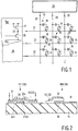
- the liquid-crystal display device of Figure 1 is similar to that of Figures 1 and 2 of GB-A-2 213 987 (our reference PHB33417).
- the device has a row and column matrix array of individual picture elements 10, only a few of which are shown in Figure 1 for simplicity. In practice there may be 105 or more such elements, for example in the case of a television display.
- Each element is defined by a pair of electrodes carried on facing surfaces of two spaced substrates (for example of glass or other low-cost insulating material) with liquid-crystal material therebetween.
- the picture-element array is located over the main central area of the substrates, whereas driving circuits 28 and 29 are located at peripheral areas.
- one substrate 14 (shown in Figure 2) carries an array of individual transparent electrodes 18 which are each generally rectangular and which are arranged together in rows and columns. Each individual electrode 18 defines the area of a respective picture element 10.
- the substrate 14 also carries a switching array of MIM devices 24 (integrated with the picture-element electrodes 18), a set of parallel row-address conductors 22, and row-driver circuitry 28 (for example the thin-film transistors 26 and 27).
- the opposite substrate (not shown in the present drawings) carries a set of parallel column-address conductors 20 connected to column-driver circuitry 29.
- the column-address conductors 20 extend at right angles to the row conductors 22. Where they overlie picture-element electrodes 18, the conductors 20 constitute the other electrodes of the picture elements 10.
- the picture-element electrodes 18 of all picture elements in the same row are connected to a respective row-address conductor 22 ( Figures 1 and 2) via associated series-connected two-terminal non-linear switching elements in the form of MIM devices 24. Although only one MIM device is shown for each picture element, two or more MIM devices 24 could be associated with each picture element 10 in known manner.
- the individual picture elements 10 are addressed in conventional fashion using scanning signals applied from the circuit 28 to each row conductor 22 in turn, and video data signals are applied appropriately, in synchronism to the column conductors 20 from the circuit 29 to modulate light transmission through the picture elements in accordance with video information.
- the elements 10 are energised on a row at a time basis so as to build up a display picture, e.g. a TV picture over one field.
- the display device and its operation are similar to known display devices using MIM type non-linear switching devices. Accordingly, the description of the device is deliberately brief, and for the most part the row and column driver circuitry is illustrated simply as circuit blocks 28 and 29 comprising known circuits.
- the row driver circuit 28 typically functions at about 30kHz
- the column driver circuit 29 functions at about 11MHz.
- Both the row and column driver circuits may be formed with thin-film transistors.
- Figure 1 illustrates two TFTs 26 and 27 connected in an inverter configuration to drive a row-address conductor 22.
- the substrate process steps used to provide the picture-element array and the driving circuits thereon involves only low substrate temperatures.
- the TFTs of the row driver circuit 28 are fabricated on the substrate 14 using manufacturing steps in accordance with the present invention.
- the TFT 26 is formed in accordance with the present invention, and comprises a body portion 36 of semiconductive crystal silicon material having a field-effect mobility in excess of 1 cm2V. ⁇ 1s ⁇ 1 so as to function satisfactorily as a row driver transistor.
- the other substrate with its column drive circuitry 29 and column conductors 20 may be produced in known manner.
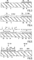
- the manufacture of the display device includes the steps of (a) depositing on the substrate 14 a layer 32 of insulating non-stoichiometric compound material of silicon alloyed with at least one other element ( Figure 4), and (b) annealing a part of that layer 32 with an energy beam 40 (for example from an excimer laser) to convert that part 36 into the semiconductive crystalline silicon material by heating with the energy beam 40 ( Figure 5).
- an energy beam 40 for example from an excimer laser
- FIGS 3 to 5 illustrate stages in the manufacture of the TFT 26 and MIM 24 of Figure 2 using a particular method in accordance with the invention which requires only three photolithographic mask alignment steps.
- one or more peripheral areas 41 of the deposited layer 32 are annealed with the energy beam 40 to provide the semiconductive crystalline silicon material for the body portions of TFTs 26,27 etc., while one or more central areas 42 of the deposited layer 32 (corresponding to the picture display area) are not exposed to the energy beam 40 and are retained on the substrate 14 as the insulating non-stoichiometric compound material of the MIM devices 24.
- the TFT 26 is of the so-called "inverted staggered type" having its gate electrode 31 adjacent to the substrate 14, and the MIM device 24 is of the vertical type having one electrode 30 also adjacent to the substrate 14.
- These electrodes 30 and 31 are formed in known manner by depositing conductive material on the substrate 14, photolithographically defining the areas to be retained, and etching away the excess material.
- both the electrodes 30 and 31 comprise two layers, for example an opaque metal 30a and 31a (such as chromium) on another material 30b and 31b which may be, for example, a transparent layer of indium tin oxide (ITO).
- ITO indium tin oxide
- the MIM electrode part 30b of the final device as shown in Figure 2 may be a small chromium-coated extension of a larger uncoated ITO area 18 which provides the picture-element electrode.
- this ITO electrode area 18 may still be coated with a corresponding chromium area 18a which is later removed.
- the ITO is not present below a TFT gate electrode 31a and MIM electrode 30a but overlaps the edge of the MIM electrode 30a to connect the MIM 24 to the transparent picture-element electrode 18 of ITO.
- the insulating non-stoichiometric compound material 32 is now
- the material 32 may be, for example, non-stoichiometric silicon nitride (SiN x ), non-stoichiometric silicon oxynitride (SiN x O y ), non-stoichiometric silicon oxide (SiO x ), and/or non-stoichiometric silicon carbide (SiC x ).
- the non-stoichiometric nature of the material 32 arises from an excess silicon content (i.e.
- the deposited material 32 also contains a high hydrogen content so that hydrogen is retained in the converted material 36 to passivate the crystal grain boundaries.
- the lattice defects due to the non-stoichiometric nature of the retained insulating material 32 have a significant role in providing the switchable non-linear current-voltage behaviour of the MIM devices 24 whereby their resistance is high at low applied voltages and drops significantly at higher applied voltages to allow adequate current to flow therethrough for the purpose of driving the picture elements 10.
- the insulating non-stoichiometric material 32 may be deposited onto a glass substrate 14 using a plasma-enhanced low-pressure chemical vapour deposition (PECVD) process.
- PECVD plasma-enhanced low-pressure chemical vapour deposition
- silicon nitride for example, a gaseous mixture of silane (SiH4) and nitrogen (N2) and hydrogen (H2) may be used for the PECVD.
- the gases are introduced into the plasma CVD reaction chamber for example at a pressure of 1 Torr (133 Pascal) and in proportions suitable to produce a silicon-rich silicon nitride material having both the desired non-linear electrical characteristics for the MIM devices 24 and the desired crystalline-silicon conversion characteristics for the TFTs 26 etc.
- the temperature of the glass substrate 14 is comparatively low during the deposition, for example about 200 o C (degrees Celsius) which is well below the softening point of the glass.
- the thickness of the deposited layer 32 may be in the range of 20 to 200nm (nanometres), for example about 100nm (i.e. 103 Angstroms).
- a gaseous mixture of silane and ammonia (NH3) and nitrous oxide (N2O) may be used.
- a gaseous mixture of silane and hydrogen and methane (CH4) may be used. It is also possible to use other material deposition techniques instead of PECVD, for example sputter deposition.
- silicon-rich non-stoichiometric silicon carbide, silicon oxide and/or silicon nitride may be deposited by reactive sputtering of a silicon target or silicon-compound target with ions using a gaseous mixture of argon with oxygen, nitrogen and other gases containing O,N and C. It is also possible to provide the layer 32 as a combination of non-stoichiometric materials for example in different layers one above the other or mixed together, and this provides a further means for controlling the desired properties of the devices 24,26 etc.
- Figure 4 illustrates the substrate after the deposition of the insulating non-stoichiometric layer 32.
- a first area 41 where the TFTs 26,27 etc are to be formed is annealed with a laser beam 40 to form polycrystalline silicon in this area 41, whereas a second area 42 where the array of MIMs 24 and picture-element electrodes 18 are to be formed is not exposed to the laser beam so that the insulating non-stoichiometric material 32 is retained unconverted in this second area 42.
- This first area 41 of the substrate 14 is mechanically scanned through the laser beam 40 which may typically have a width of about 6mm. The dimensions (together with the positioning of the substrate 14 in the laser equipment) are such that there is no need for any mask over the picture-element array area 42 to prevent it from exposure to the laser beam 40.
- an excimer laser is used in the specific example of Figures 2 to 5, so as to generate the beam 40 at an ultraviolet wavelength (for example at 248nm for a KrF laser) having a shallow absorption depth in the deposited layer 32.
- Tile thickness of the crystalline silicon produced by the laser beam 40 is much deeper than the absorption depth which is typically about 6nm (60 Angstroms) for excimer ultraviolet wavelengths.
- the greater depth of crystallization is due to the strong heating effect of the absorbed energy apparently leading to a melting of the material 32.
- the melting of the material results in some reduction of the other-element (i.e. non-silicon) content of the material, apparently by gaseous evolution.
- the incident laser energy in the range 100 to 300 mJ.cm ⁇ 1 per pulse, the depth over which the insulating material 32 is converted into semiconductive crystalline silicon material 36 can be varied from less than 10nm (100 Angstroms) to about 60 or 70nm (600 to 700 Angstroms).
- the thickness of the semiconductive crystalline silicon body portion 36 of the TFT 26 can be controlled by controlling the laser energy.
- the gate insulator of this TFT 26 is provided by the unconverted insulating material 32a between the underlying gate 31 and overlying crystalline silicon 36 of the TFT channel region, and so the thickness of the gate insulator 32a can be determined by appropriate choice of the original thickness of the deposited layer 32 and of the energy of the laser beam 40.
- FIG. 5 The structure of Figure 5 is then further processed in known manner to define the body portions for the MIM devices 24 and TFTs 26 etc. This involves a photolithographic and etching stage for etching away excess areas of the layers 32,36 and 32a. In removing the insulating material 32 from over the picture-element electrode 18, the chromium area 18a is exposed and is now etched away so that this picture-element area becomes transparent.
- a further photolithographic and etching stage is then carried out to provide a pattern of conductor tracks 22,23 etc. and electrodes 51,52,53 etc. as top connections and interconnections for the TFTs 26,27 etc. and the MIM devices 24.
- the top electrodes 51,52,53 etc. may be of, for example, chromium.
- the electrodes 51 and 52 are provided on the semiconductor crystalline silicon material 36 of the TFT channel region and form the source and drain of the TFT 26.
- the electrodes 53 are provided on the insulating material 32 of the MIM device 24 and provide the second terminal of the MIM.
- the crystalline silicon material 36 produced by heating the insulating material 32 with the laser beam 40 is of surprisingly good quality for producing semiconductor devices, in spite of the material 32 having been deposited at a low temperature. Spectroscopy measurements show that polycrystalline silicon material of large grain size is produced.
- an amorphous non-stoichiometric silicon nitride material 32 formed by the described PECVD process was heated with a KrF excimer laser beam of 248nm wavelength operated at a low duty cycle of a few hertz with a pulse width of 20ns and an energy of 200 mJ.cm ⁇ 2 per pulse; the resulting crystalline silicon material consisted of silicon crystal grains with some Si3N4 inclusions in the layer structure.
- the average crystal grain size at the surface of the crystalline material 36 is found to increase with increasing incident energy in the range 150 to 250 mJ.cm ⁇ 2 per pulse, and this results in an increase in the field-effect mobility, for example in the range of 5 to 15 cm2.V ⁇ 1.s ⁇ 1.
- the silicon crystalline material 36 was also thought to be hydrogenated by retention of some of the hydrogen content of the PECVD material 32. This hydrogen content appears to improve the device quality of the material 36 by passivating the silicon crystal grain boundaries in the material 36 and by passivating the interface between the crystallized silicon material 36 and the underlying part 32a of unconverted insulating material 32 (for example in the TFT gate insulator structure).
- the composition of the crystallized silicon layer 36 it appears to consist of silicon crystal grains with some Si3N4 inclusions. Some of the nitrogen content of the original material 32 has been lost from the crystallized material 36 apparently by evolution of N2 gas during the molten phase. Furthermore, some n-type doping of the crystallized silicon 36 by the nitrogen also seems to occur.
- the conductivity of the crystallized silicon 36 can be controlled by including p-type dopant to at least partially compensate for the nitrogen doping. Alternatively, nitrogen doping of the silicon 36 can be reduced or avoided by using a diffferent starting material 32, for example silicon oxynitride, silicon oxide or silicon carbide etc.
- a part of the gate insulator may be provided as a further insulating layer formed on the gate 31 ( Figure 3) before depositing the MIM layer 32 of insulating non-stoichiometric compound material ( Figure 4).
- This further insulating layer may be deposited, or it may be formed by converting the surface of the metal gate for example by anodisation or oxidation of a tantalum, or aluminium or titanium gate 31.
- any remaining part 32a of the insulating non-stoichiometric material not converted by the beam 40 may serve to reduce strain between the overlying crystalline silicon material 36 and underlying the gate insulator.
- Such a further insulating layer may also be provided over the MIM electrode 30 in Figure 3 and serve in the final MIM device 24 to further control the non-linear resistance characteristics of this device.
- the unconverted part 32a of the insulating non-stoichiometric compound material not only provides at least part of the gate insulator in the channel area of the TFT 26 but also provides an interface between the semiconductive crystalline silicon material 36 and the substrate 14 in the areas beyond the channel area.
- This interface 32a may reduce strain between the overlying crystalline silicon material 36 and the underlying substrate 14.
- converting the layer 32 into crystalline silicon material over only a part of its thickness is advantageous in preserving good adhesive of the layers 32,36 etc. to the substrate 14.
- the applicants have also annealed layers 32 using an argon laser operating in the visible green wavelength region (instead of ultraviolet from an excimer laser) and find that although the layer 32 is converted through its thickness there is a tendancy for the converted layer 36 to peel away from the substrate 14. This tendancy to peel appears to result from strong heating of the substrate during the exposure of the overlying layer 32 to the laser beam, even though that exposure is of short duration.
- the penetration depth of this argon laser beam 40 is several times that of an excimer laser.
- FIG 6 illustrates another embodiment in which the layer 32 is converted into crystalline silicon material 36 over only a part of its thickness so as to leave an insulating interface 32a with the substrate 14.
- no electrodes are formed on the substrate 14 (compare with Figure 3) before depositing the layer 32 (compare with Figure 4), and after the conversion treatment with the beam 40 (compare with Figure 5) all the device electrodes for the TFT 26 and MIM 24 are provided on the top face of the layers 36 and 32.
- a TFT 26 of the so-called "coplanar" type is formed having source and drain electrodes 51 and 52, a gate insulator 55 and gate 31.
- This TFT 26 may be fabricated on the converted silicon layer 36 in a similar manner to that described in published European patent application EP-A-0 523 768 published on 20th January 1993 and having a GB priority date of 28th June 1991.
- the whole contents of EP-A-0 523 768 (our reference PHB33727) are hereby incorporated herein as reference material.
- the MIM 24 is of the lateral type in this embodiment, and may be fabricated on the retained insulating non-stoichiometric compound material 32 in a similar manner to that described in published United Kingdom patent application GB-A-2 244 860 (our reference PHB33633), the whole contents of which are hereby incorporated herein as reference material.
- Figure 1 illustrates an embodiment of the present invention in the manufacture of a liquid-crystal display device in which a liquid-crystal film is encapsulated between the substrate 14 and another substrate carrying the column conductors 20 and having the column driving circuitry 29.
- the display may be for an instrument panel or for a personal computer display panel or for a television receiver.
- a display device manufactured in accordance with the present invention may be designed to operate with another electro-optical material (for example, an electropheretic suspension or electrochromic material) between the two substrates.
- another electro-optical material for example, an electropheretic suspension or electrochromic material
- the device may be an image sensor having a switching array of MIM devices 24 which serves for addressing an image sensing array and which is driven by circuitry comprising TFTs fabricated in semiconductive crystalline silicon material 36 formed in accordance with the invention.
- the electronic device manufactured in accordance with the invention may be a data store comprising a switching array of MIM devices 24 which serves for addressing an array of storage devices (for example, capacitors).
- the switch array of such a data store may be addressed by transverse sets of column and row conductors 20 and 22, both of which may be carried on the same substrate 14.
- both the row and column circuitry 28 and 29 may be formed in semiconductive crystalline silicon material 36 provided in accordance with the present invention on the same substrate 14.
- the semiconductor devices formed in the semiconductive crystalline silicon material 36 are thin-film transistors having an insulated gate (31,32a) as its control electrode.
- other semiconductor devices may be fabricated, for example a semiconductor diode.
- a bipolar thin-film transistor may be formed having a base contact as its control electrode for controlling current flow through a base region formed in the semiconductive crystalline silicon material.
- the insulating non-stoichiometric compound material 32 may comprise a dopant element such as phosphorus, for example as disclosed in EP-A-0 202 092.
- the inclusion of the dopant element in the material 32 can also be advantageous for a semiconductor device 26, in doping the semiconductive crystalline silicon material 36 which is formed from the material 32 by annealing with a laser beam 40 in accordance with the present invention.
- any retained insulating material 32 may be used for another purpose, for example for electrical insulation between active devices or between device circuitry areas which are formed in the semiconductive crystalline silicon material.
- semiconductive crystalline silicon material 36 formed in accordance with the present invention may be used to form semiconductor devices in the switching array of a display or imaging device or data store, if so desired.
- a laser was used to generate the energy beam 40.
- a laser beam is particularly convenient for controlling the annealing and heating conditions.
- other forms of energy beam for example an electron beam or high-power lamps
- the conversion to crystalline silicon material may be effected by a short-duration exposure to very high intensity lamps, and a stencil mask plate may be used to localize this exposure so as to protect areas 42 which are not to be converted.
Abstract

Description
- This invention relates to methods of manufacturing an electronic device comprising at least one semiconductor device (for example a thin-film transistor) which has a body portion of semiconductive crystalline silicon material formed by annealing with an energy beam, and further relates to devices manufactured by such methods. The invention relates particularly but not exclusively to the manufacture of electronic devices wherein the semiconductor devices provide circuitry for driving an array of switching devices formed on the same substrate as the semiconductor devices. Such switching devices may be of the MIM-type, and the electronic device may be, for example, a liquid-crystal display or a data store.
- For very many years amorphous-silicon thin-film transistors (TFTs) were used as the switching devices in an array for actively controlling the operation of the picture elements of a liquid-crystal display. In more recent years MIM-type devices have been used instead of thin-film transistors, because the MIM-type devices have only two terminal electrodes and are comparatively simple to manufacture.
- A MIM type device is a type of switching diode having a non-linear current-voltage characteristic through one or more layers of insulating material between two metallic (i.e. conductive) layers which form the diode electrodes. Hence the acronym "MIM" is derived from the English "Metallic-Insulative-Metallic". Published United Kingdom patent applications GB-A-2 213 987 (our reference PHB33417) and GB-A-2 231 200 (our reference PHB33547), and published European patent applications EP-A-0 182 484, EP-A-0 202 092 and EP-A-0 333 392 describe the fabrication of MIM-type diodes with non-stoichiometric silicon-based compounds, for example silicon nitride, silicon oxide, silicon oxynitride and/or silicon carbide as the insulative material, and further describe their use as switching devices in arrays for the active matrix addressing of a liquid-crystal display. The MIM-type diodes in the array are switched on by applying sequentially a moderately high scanning voltage signal (for example in the range of 10 to 15 volts) to row conductors of the display. The whole contents of GB-A-2 213 987, GB-A-2 231 200, EP-A-0 182 484, EP-A-0 202 092, and EP-A-0 333 392 are hereby incorporated herein as reference material.
- Preferably the driving circuitry for addressing such an array is integrated on the same substrate as the array so as to reduce the number of external connections. Typically the substrate is of a low-cost material such as a glass or plastics material, and so only low-temperature processing steps should be used to fabricate the driving circuitry. Therefore preferably the semiconductor device technology used to fabricate the driving circuitry should not involve heating the substrate (at least for any significant time) to temperatures above, for example, about 700oC.
- When the switching array is formed of thin-film transistors, the driving circuitry can also be formed of thin-film transistors integrated on the display substrate(s). Thus, row drivers may be formed with thin film transistors having a sufficiently high mobility to allow the row conductors to be scanned at, for example, about 30kHz for a television display device. In simple terms, the field-effect mobility needs to be in excess of about 1cm².V⁻¹.s⁻¹ to achieve this scanning rate, and this high mobility can be achieved in silicon crystalline material formed by depositing a layer on a substrate and annealing at least a part of the layer with an energy beam. Specific examples using a CW argon laser beam are described in the articles "High-voltage polysilicon TFTs with multi-channel structure" by T. Unagami in IEEE Transactions on Electron Devices Vol. 35 No. 12, December 1988, pages 2363 to 2367, "Low Temperature Fabrication of Poly-Si TFT by Laser Induced Crystallization of a-Si" by Masumo et. al. in Journal of Non-Crystalline Solids Vol. 115 (1989) pages 147 to 149, and "A laser-recrystallization technique for silicon-TFT integrated circuits on quartz substrates, and its application to small-size monolithic active-matrix LCDs" by E. Fujii et. al. in IEEE Transactions on Electron Devices Vol. 37 No. 1, January 1990, pages 121 to 127. The whole contents of all these articles are hereby incorporated herein as reference material. In this known laser-annealed device process technology, the deposited layer is of semiconductive amorphous or small-grain silicon and is annealed into large-grain polycrystalline silicon (polysilicon) by heating with the laser beam. This technology provides satisfactory TFTs to form the driving circuitry of the TFT switching array.
- However, the driving circuits for a MIM device array cannot be fabricated as MIM-type devices, and so a different device technology with different materials is required on the substrate when the switching array is formed of MIM-type devices.
- It is an aim of the present invention to mitigate this disadvantage of incompatibility of MIM device technology with driving-circuit device technology, and in particular to provide an alternative way of forming suitable semiconductive material for semiconductor devices in a manner which may still be compatible with low-temperature processing for the device substrate(s).
- The present invention is based on a surprising discovery by the present inventor that body portions of semiconductive crystalline silicon material of a sufficient quality to form high-mobility thin-film transistors and other semiconductor devices can be formed by (a) depositing a layer of insulating silicon-based non-stoichiometric compound material and then (b) converting this material into the semiconductive crystalline silicon material by heating with an energy beam.
- Thus, according to the present invention, there is provided a method of manufacturing an electronic device comprising at least one semiconductor device which has a body portion of semiconductive crystalline silicon material, wherein the silicon crystalline material is formed by depositing a layer on a substrate and annealing at least a part of the layer with an energy beam, which method is characterised in that the layer is deposited as an insulating non-stoichiometric compound material of silicon alloyed with at least one other element, and in that at least a part of the insulating non-stoichiometric compound material is converted into the semiconductive crystalline silicon material by heating that part with the energy beam.
- A versatile device process technology results from the use of an energy beam to convert the insulating compound material into semiconductive crystalline silicon material, and the resulting process technology can be maintained compatible with individual low-temperature requirements for processing particular low-cost substrates. The whole layer may be converted to the semiconductive silicon material. However, the wavelength and energy of the beam (for example most conveniently from a laser) and the area of the layer exposed thereto can be controlled so as to control which parts of the deposited layer are converted and which parts are not converted. This permits localization of the conversion in the vertical direction of the thickness of the layer and in the longitudinal direction of the surface area of the layer.
- Thus, by selectively masking or directing the energy beam, a first area of the deposited layer may be annealed with the energy beam to provide the semiconductive crystalline silicon material for the semiconductive device, and a second area of the deposited layer which is not subjected to the energy beam may be retained on the substrate as insulating non-stoichiometric compound material in the manufactured electronic device. This second area may provide a simple insulating function in the manufactured device, for example between active semiconductor devices or device areas.
- However the present inventor has also discovered that the deposited layer of insulating non-stoichiometric compound material may be of a type suitable for forming a MIM-type switching device, for example a non-stoichiometric silicon nitride, silicon oxide, silicon oxynitride and/or silicon carbide. Indeed, from the insulating materials already used for forming MIM devices, silicon-rich ranges may be selected for conversion into semiconductive crystalline silicon by annealing with an energy beam in accordance with the present invention. Thus, the present inventor has also devised a method of fabricating high-mobility semiconductor devices such as row-driver thin-film transistors in a manner compatible with the manufacture of a MIM switching array. A first area of the layer of insulating non-stoichiometric compound material may be converted by the energy beam into the semiconductive crystalline silicon material for a thin-film transistor or other semiconductor device, whereas a second area is retained and provided with two electrodes to form a MIM-type switching device on the substrate.
- The exposed area(s) of the deposited layer may be converted throughout the layer thickness into the semiconductor crystalline silicon material. However the use of an energy beam permits the choice of a short beam-wavelength having an absorption depth in the deposited layer which is so much less than the thickness of the deposited layer that the insulating non-stoichiometric compound material is converted into semiconductive crystalline silicon material over only a part of its thickness. This reduces the heating of the substrate by the energy beam and is particularly useful for forming the devices on a low-cost low-temperature substrate. The underlying unconverted part may be used to provide an insulating interface between the semiconductive crystalline silicon material and the substrate.
- However, an underlying unconverted part of the layer may be used as an active part of the semiconductor device. Thus, for example, the semiconductor device may be a thin-film transistor having a gate which is formed on the substrate before depositing the layer; in this case the semiconductor crystalline silicon material provides a channel region of the transistor, and an unconverted part of the insulating non-stoichiometric compound material may provide at least a part of a gate insulator between the underlying gate and the overlying channel region. This provides a simple method for fabricating an insulated-gate TFT.
- These and other features in accordance with the invention are illustrated specifically in embodiments of the invention now to be described, by way of example, with reference to the accompanying diagrammatic drawings. In these drawings:
- Figure 1 is a partial circuit diagram of part of a liquid-crystal display device including a MIM switching array driven by TFT circuitry;
- Figure 2 is a cross-sectional view of part of one substrate of the display device of Figure 1 and showing a MIM switching device and a TFT driver formed on different areas of the substrate by using manufacturing steps in accordance with the present invention;
- Figures 3 to 5 are cross-sectional views of the device part of Figure 2 at successive stages in the manufacture, and
- Figure 6 is a cross-sectional view of a part of one substrate of another display device and showing other types of MIM switching device and TFT driver formed on the substrate by using manufacturing steps in accordance with the invention.
- It should be noted that all the drawings are diagrammatic and not drawn to scale. Relative dimensions and proportions of parts of the Figures have been shown exaggerated or reduced in size for the sake of clarity and convenience in the drawings. The same reference signs are generally used to refer to corresponding or similar features in the different embodiments.
- Except for the manner in which its MIM switching devices and TFT driving circuitry is fabricated, the liquid-crystal display device of Figure 1 is similar to that of Figures 1 and 2 of GB-A-2 213 987 (our reference PHB33417). The device has a row and column matrix array of
individual picture elements 10, only a few of which are shown in Figure 1 for simplicity. In practice there may be 10⁵ or more such elements, for example in the case of a television display. Each element is defined by a pair of electrodes carried on facing surfaces of two spaced substrates (for example of glass or other low-cost insulating material) with liquid-crystal material therebetween. The picture-element array is located over the main central area of the substrates, whereas drivingcircuits - More particularly, one substrate 14 (shown in Figure 2) carries an array of individual
transparent electrodes 18 which are each generally rectangular and which are arranged together in rows and columns. Eachindividual electrode 18 defines the area of arespective picture element 10. Thesubstrate 14 also carries a switching array of MIM devices 24 (integrated with the picture-element electrodes 18), a set of parallel row-address conductors 22, and row-driver circuitry 28 (for example the thin-film transistors 26 and 27). - The opposite substrate (not shown in the present drawings) carries a set of parallel column-
address conductors 20 connected to column-driver circuitry 29. The column-address conductors 20 extend at right angles to therow conductors 22. Where they overlie picture-element electrodes 18, theconductors 20 constitute the other electrodes of thepicture elements 10. - The picture-
element electrodes 18 of all picture elements in the same row are connected to a respective row-address conductor 22 (Figures 1 and 2) via associated series-connected two-terminal non-linear switching elements in the form ofMIM devices 24. Although only one MIM device is shown for each picture element, two ormore MIM devices 24 could be associated with eachpicture element 10 in known manner. - The
individual picture elements 10 are addressed in conventional fashion using scanning signals applied from thecircuit 28 to eachrow conductor 22 in turn, and video data signals are applied appropriately, in synchronism to thecolumn conductors 20 from thecircuit 29 to modulate light transmission through the picture elements in accordance with video information. Theelements 10 are energised on a row at a time basis so as to build up a display picture, e.g. a TV picture over one field. - The display device and its operation are similar to known display devices using MIM type non-linear switching devices. Accordingly, the description of the device is deliberately brief, and for the most part the row and column driver circuitry is illustrated simply as circuit blocks 28 and 29 comprising known circuits. For a TV display, the
row driver circuit 28 typically functions at about 30kHz, whereas thecolumn driver circuit 29 functions at about 11MHz. Both the row and column driver circuits may be formed with thin-film transistors. By way of example, Figure 1 illustrates twoTFTs address conductor 22. - Because the low-cost substrates are not able to withstand device-processing at high temperatures, the substrate process steps used to provide the picture-element array and the driving circuits thereon involves only low substrate temperatures. The TFTs of the
row driver circuit 28 are fabricated on thesubstrate 14 using manufacturing steps in accordance with the present invention. Thus, for example theTFT 26 is formed in accordance with the present invention, and comprises abody portion 36 of semiconductive crystal silicon material having a field-effect mobility in excess of 1 cm²V.⁻¹s⁻¹ so as to function satisfactorily as a row driver transistor. The other substrate with itscolumn drive circuitry 29 andcolumn conductors 20 may be produced in known manner. - Thus, in accordance with the present invention, the manufacture of the display device includes the steps of (a) depositing on the substrate 14 a
layer 32 of insulating non-stoichiometric compound material of silicon alloyed with at least one other element (Figure 4), and (b) annealing a part of thatlayer 32 with an energy beam 40 (for example from an excimer laser) to convert thatpart 36 into the semiconductive crystalline silicon material by heating with the energy beam 40 (Figure 5). - Figures 3 to 5 illustrate stages in the manufacture of the
TFT 26 andMIM 24 of Figure 2 using a particular method in accordance with the invention which requires only three photolithographic mask alignment steps. In this method one or moreperipheral areas 41 of the deposited layer 32 (corresponding to the areas of the drive circuitry 28) are annealed with the energy beam 40 to provide the semiconductive crystalline silicon material for the body portions ofTFTs central areas 42 of the deposited layer 32 (corresponding to the picture display area) are not exposed to the energy beam 40 and are retained on thesubstrate 14 as the insulating non-stoichiometric compound material of theMIM devices 24. - In this particular example, the
TFT 26 is of the so-called "inverted staggered type" having itsgate electrode 31 adjacent to thesubstrate 14, and theMIM device 24 is of the vertical type having oneelectrode 30 also adjacent to thesubstrate 14. Theseelectrodes substrate 14, photolithographically defining the areas to be retained, and etching away the excess material. - In the specific example illustrated in Figures 2 to 5, both the
electrodes opaque metal material MIM electrode part 30b of the final device as shown in Figure 2 may be a small chromium-coated extension of a largeruncoated ITO area 18 which provides the picture-element electrode. At the stage illustrated in Figures 3 to 5 however, thisITO electrode area 18 may still be coated with a correspondingchromium area 18a which is later removed. However, other arrangements are possible in which the ITO is not present below aTFT gate electrode 31a andMIM electrode 30a but overlaps the edge of theMIM electrode 30a to connect theMIM 24 to the transparent picture-element electrode 18 of ITO. The insulatingnon-stoichiometric compound material 32 is now - deposited on the
substrate 14 and over theelectrode pattern material 32 may be, for example, non-stoichiometric silicon nitride (SiNx), non-stoichiometric silicon oxynitride (SiNxOy), non-stoichiometric silicon oxide (SiOx), and/or non-stoichiometric silicon carbide (SiCx). The non-stoichiometric nature of thematerial 32 arises from an excess silicon content (i.e. greater than the stoichiometric ratio of the compound) and a deficiency of the other element, and this facilitates the conversion of the insulatingmaterial 32 upon heating with the energy beam 40 into the semiconductivecrystalline silicon material 36 for the body portions of theTFTs material 32 also contains a high hydrogen content so that hydrogen is retained in the convertedmaterial 36 to passivate the crystal grain boundaries. Furthermore, the lattice defects due to the non-stoichiometric nature of the retained insulatingmaterial 32 have a significant role in providing the switchable non-linear current-voltage behaviour of theMIM devices 24 whereby their resistance is high at low applied voltages and drops significantly at higher applied voltages to allow adequate current to flow therethrough for the purpose of driving thepicture elements 10. - The insulating
non-stoichiometric material 32 may be deposited onto aglass substrate 14 using a plasma-enhanced low-pressure chemical vapour deposition (PECVD) process. In the case of silicon nitride, for example, a gaseous mixture of silane (SiH₄) and nitrogen (N₂) and hydrogen (H₂) may be used for the PECVD. The gases are introduced into the plasma CVD reaction chamber for example at a pressure of 1 Torr (133 Pascal) and in proportions suitable to produce a silicon-rich silicon nitride material having both the desired non-linear electrical characteristics for theMIM devices 24 and the desired crystalline-silicon conversion characteristics for theTFTs 26 etc. The temperature of theglass substrate 14 is comparatively low during the deposition, for example about 200oC (degrees Celsius) which is well below the softening point of the glass. Depending on the desired device characteristics for both theMIMs 24 andTFTs 26, the thickness of the depositedlayer 32 may be in the range of 20 to 200nm (nanometres), for example about 100nm (i.e. 10³ Angstroms). - In the case of plasma CVD of silicon oxynitride, a gaseous mixture of silane and ammonia (NH₃) and nitrous oxide (N₂O) may be used. For plasma enhanced CVD of a non-stoichiometric silicon carbide, a gaseous mixture of silane and hydrogen and methane (CH₄) may be used. It is also possible to use other material deposition techniques instead of PECVD, for example sputter deposition. Thus, for example, silicon-rich non-stoichiometric silicon carbide, silicon oxide and/or silicon nitride may be deposited by reactive sputtering of a silicon target or silicon-compound target with ions using a gaseous mixture of argon with oxygen, nitrogen and other gases containing O,N and C. It is also possible to provide the
layer 32 as a combination of non-stoichiometric materials for example in different layers one above the other or mixed together, and this provides a further means for controlling the desired properties of thedevices - Figure 4 illustrates the substrate after the deposition of the insulating
non-stoichiometric layer 32. In the next stage which is illustrated in Figure 5, afirst area 41 where theTFTs area 41, whereas asecond area 42 where the array ofMIMs 24 and picture-element electrodes 18 are to be formed is not exposed to the laser beam so that the insulatingnon-stoichiometric material 32 is retained unconverted in thissecond area 42. Thisfirst area 41 of thesubstrate 14 is mechanically scanned through the laser beam 40 which may typically have a width of about 6mm. The dimensions (together with the positioning of thesubstrate 14 in the laser equipment) are such that there is no need for any mask over the picture-element array area 42 to prevent it from exposure to the laser beam 40. - Preferably an excimer laser is used in the specific example of Figures 2 to 5, so as to generate the beam 40 at an ultraviolet wavelength (for example at 248nm for a KrF laser) having a shallow absorption depth in the deposited
layer 32. Tile thickness of the crystalline silicon produced by the laser beam 40 is much deeper than the absorption depth which is typically about 6nm (60 Angstroms) for excimer ultraviolet wavelengths. The greater depth of crystallization is due to the strong heating effect of the absorbed energy apparently leading to a melting of thematerial 32. The melting of the material results in some reduction of the other-element (i.e. non-silicon) content of the material, apparently by gaseous evolution. Thus, in the case of asilicon nitride layer 32, some compositional change occurs with loss of some of the nitrogen content by evolution of N₂ gas. By varying the incident laser energy in the range 100 to 300 mJ.cm⁻¹ per pulse, the depth over which the insulatingmaterial 32 is converted into semiconductivecrystalline silicon material 36 can be varied from less than 10nm (100 Angstroms) to about 60 or 70nm (600 to 700 Angstroms). - Thus, in the specific example of Figures 2 to 5, the thickness of the semiconductive crystalline
silicon body portion 36 of theTFT 26 can be controlled by controlling the laser energy. The gate insulator of thisTFT 26 is provided by the unconverted insulatingmaterial 32a between theunderlying gate 31 and overlyingcrystalline silicon 36 of the TFT channel region, and so the thickness of thegate insulator 32a can be determined by appropriate choice of the original thickness of the depositedlayer 32 and of the energy of the laser beam 40. - The structure of Figure 5 is then further processed in known manner to define the body portions for the
MIM devices 24 andTFTs 26 etc. This involves a photolithographic and etching stage for etching away excess areas of thelayers material 32 from over the picture-element electrode 18, thechromium area 18a is exposed and is now etched away so that this picture-element area becomes transparent. - A further photolithographic and etching stage is then carried out to provide a pattern of conductor tracks 22,23 etc. and
electrodes TFTs MIM devices 24. Thetop electrodes electrodes crystalline silicon material 36 of the TFT channel region and form the source and drain of theTFT 26. Theelectrodes 53 are provided on the insulatingmaterial 32 of theMIM device 24 and provide the second terminal of the MIM. - The
crystalline silicon material 36 produced by heating the insulatingmaterial 32 with the laser beam 40 is of surprisingly good quality for producing semiconductor devices, in spite of the material 32 having been deposited at a low temperature. Spectroscopy measurements show that polycrystalline silicon material of large grain size is produced. - In a particular example an amorphous non-stoichiometric
silicon nitride material 32 formed by the described PECVD process was heated with a KrF excimer laser beam of 248nm wavelength operated at a low duty cycle of a few hertz with a pulse width of 20ns and an energy of 200 mJ.cm⁻² per pulse; the resulting crystalline silicon material consisted of silicon crystal grains with some Si₃N₄ inclusions in the layer structure. The average crystal grain size at the surface of thecrystalline material 36 is found to increase with increasing incident energy in the range 150 to 250 mJ.cm⁻² per pulse, and this results in an increase in the field-effect mobility, for example in the range of 5 to 15 cm².V⁻¹.s⁻¹. Thesilicon crystalline material 36 was also thought to be hydrogenated by retention of some of the hydrogen content of thePECVD material 32. This hydrogen content appears to improve the device quality of thematerial 36 by passivating the silicon crystal grain boundaries in thematerial 36 and by passivating the interface between thecrystallized silicon material 36 and theunderlying part 32a of unconverted insulating material 32 (for example in the TFT gate insulator structure). - As regards the composition of the crystallized
silicon layer 36, it appears to consist of silicon crystal grains with some Si₃N₄ inclusions. Some of the nitrogen content of theoriginal material 32 has been lost from the crystallizedmaterial 36 apparently by evolution of N₂ gas during the molten phase. Furthermore, some n-type doping of the crystallizedsilicon 36 by the nitrogen also seems to occur. The conductivity of the crystallizedsilicon 36 can be controlled by including p-type dopant to at least partially compensate for the nitrogen doping. Alternatively, nitrogen doping of thesilicon 36 can be reduced or avoided by using adiffferent starting material 32, for example silicon oxynitride, silicon oxide or silicon carbide etc. - It will be evident that many modifications and variations are possible. Thus, for example while retaining the inverted staggered configuration for the
TFT 26 in Figures 2 to 5, a part of the gate insulator may be provided as a further insulating layer formed on the gate 31 (Figure 3) before depositing theMIM layer 32 of insulating non-stoichiometric compound material (Figure 4). This further insulating layer may be deposited, or it may be formed by converting the surface of the metal gate for example by anodisation or oxidation of a tantalum, or aluminium ortitanium gate 31. This permits the provision of a very high quality dielectric for the gate insulator, and any remainingpart 32a of the insulating non-stoichiometric material not converted by the beam 40 may serve to reduce strain between the overlyingcrystalline silicon material 36 and underlying the gate insulator. In this case, it is even possible to convert the material 32 to semiconductive crystalline silicon material over its whole thickness while retaining the further insulating layer as the sole gate insulator of theTFT 26. Such a further insulating layer may also be provided over theMIM electrode 30 in Figure 3 and serve in thefinal MIM device 24 to further control the non-linear resistance characteristics of this device. - In the embodiment of Figures 2 to 5, the
unconverted part 32a of the insulating non-stoichiometric compound material not only provides at least part of the gate insulator in the channel area of theTFT 26 but also provides an interface between the semiconductivecrystalline silicon material 36 and thesubstrate 14 in the areas beyond the channel area. Thisinterface 32a may reduce strain between the overlyingcrystalline silicon material 36 and theunderlying substrate 14. Furthermore converting thelayer 32 into crystalline silicon material over only a part of its thickness is advantageous in preserving good adhesive of thelayers substrate 14. Thus, for example, the applicants have also annealedlayers 32 using an argon laser operating in the visible green wavelength region (instead of ultraviolet from an excimer laser) and find that although thelayer 32 is converted through its thickness there is a tendancy for the convertedlayer 36 to peel away from thesubstrate 14. This tendancy to peel appears to result from strong heating of the substrate during the exposure of theoverlying layer 32 to the laser beam, even though that exposure is of short duration. The penetration depth of this argon laser beam 40 is several times that of an excimer laser. - Figure 6 illustrates another embodiment in which the
layer 32 is converted intocrystalline silicon material 36 over only a part of its thickness so as to leave an insulatinginterface 32a with thesubstrate 14. In this embodiment no electrodes are formed on the substrate 14 (compare with Figure 3) before depositing the layer 32 (compare with Figure 4), and after the conversion treatment with the beam 40 (compare with Figure 5) all the device electrodes for theTFT 26 andMIM 24 are provided on the top face of thelayers TFT 26 of the so-called "coplanar" type is formed having source and drainelectrodes gate insulator 55 andgate 31. ThisTFT 26 may be fabricated on the convertedsilicon layer 36 in a similar manner to that described in published European patent application EP-A-0 523 768 published on 20th January 1993 and having a GB priority date of 28th June 1991. The whole contents of EP-A-0 523 768 (our reference PHB33727) are hereby incorporated herein as reference material. TheMIM 24 is of the lateral type in this embodiment, and may be fabricated on the retained insulatingnon-stoichiometric compound material 32 in a similar manner to that described in published United Kingdom patent application GB-A-2 244 860 (our reference PHB33633), the whole contents of which are hereby incorporated herein as reference material. - Figure 1 illustrates an embodiment of the present invention in the manufacture of a liquid-crystal display device in which a liquid-crystal film is encapsulated between the
substrate 14 and another substrate carrying thecolumn conductors 20 and having thecolumn driving circuitry 29. The display may be for an instrument panel or for a personal computer display panel or for a television receiver. Instead of a liquid crystal material, a display device manufactured in accordance with the present invention may be designed to operate with another electro-optical material (for example, an electropheretic suspension or electrochromic material) between the two substrates. - Furthermore, instead of a display device, a different type of electronic device may be manufactured in accordance with the present invention. Thus, for example, the device may be an image sensor having a switching array of
MIM devices 24 which serves for addressing an image sensing array and which is driven by circuitry comprising TFTs fabricated in semiconductivecrystalline silicon material 36 formed in accordance with the invention. In another form, the electronic device manufactured in accordance with the invention may be a data store comprising a switching array ofMIM devices 24 which serves for addressing an array of storage devices (for example, capacitors). The switch array of such a data store may be addressed by transverse sets of column androw conductors same substrate 14. In this case both the row andcolumn circuitry crystalline silicon material 36 provided in accordance with the present invention on thesame substrate 14. - In the embodiments of Figures 2 to 6, the semiconductor devices formed in the semiconductive
crystalline silicon material 36 are thin-film transistors having an insulated gate (31,32a) as its control electrode. However other semiconductor devices may be fabricated, for example a semiconductor diode. A bipolar thin-film transistor may be formed having a base contact as its control electrode for controlling current flow through a base region formed in the semiconductive crystalline silicon material. - Having regard to desired characteristics for a
MIM device 24, the insulatingnon-stoichiometric compound material 32 may comprise a dopant element such as phosphorus, for example as disclosed in EP-A-0 202 092. The inclusion of the dopant element in thematerial 32 can also be advantageous for asemiconductor device 26, in doping the semiconductivecrystalline silicon material 36 which is formed from thematerial 32 by annealing with a laser beam 40 in accordance with the present invention. - In the embodiments of Figures 2 to 6, areas of the insulating
non-stoichiometric compound material 32 are retained to form theswitchable MIM devices 24. However the present invention may be used to manufacture devices without MIM devices. Thus, any retained insulatingmaterial 32 may be used for another purpose, for example for electrical insulation between active devices or between device circuitry areas which are formed in the semiconductive crystalline silicon material. Furthermore semiconductivecrystalline silicon material 36 formed in accordance with the present invention may be used to form semiconductor devices in the switching array of a display or imaging device or data store, if so desired. - In the embodiments described with reference to Figures 2 to 6, a laser was used to generate the energy beam 40. A laser beam is particularly convenient for controlling the annealing and heating conditions. However, other forms of energy beam (for example an electron beam or high-power lamps) may be used to fabricate the semiconductive
crystalline silicon material 36 from the insulatingnon-stoichiometric compound material 32. Thus, the conversion to crystalline silicon material may be effected by a short-duration exposure to very high intensity lamps, and a stencil mask plate may be used to localize this exposure so as to protectareas 42 which are not to be converted. - From reading the present disclosure, other variations and modifications will be apparent to persons skilled in the art. Such variations and modifications may involve equivalents and other features which are already known in semiconductor and thin film technologies and in the design, manufacture and use of displays and other large-area electronic devices and component parts thereof, and which may be used instead of or in addition to features already described herein. Although claims have been formulated in this application to particular combinations of features, it should be understood that the scope of the disclosure of the present application also includes any novel feature or any novel combination of features disclosed herein either explicitly or implicitly or any generalisation thereof, whether or not it relates to the same invention as presently claimed in any claim and whether or not it mitigates any or all of the same technical problems as does the present invention. The applicants hereby give notice that new claims may be formulated to such features and/or combinations of such features during the prosecution of the present application or of any further application derived therefrom.
Claims (12)
- A method of manufacturing an electronic device comprising at least one semiconductor device which has a body portion of semiconductive crystalline silicon material, wherein the silicon crystalline material is formed by depositing a layer on a substrate and annealing at least a part of the layer with an energy beam, which method is characterised in that the layer is deposited as an insulating non-stoichiometric compound material of silicon alloyed with at least one other element, and in that at least a part of the insulating non-stoichiometric compound material is converted into the semiconductive crystalline silicon material by heating that part with the energy beam.
- A method as claimed in claim 1, further characterised in that a first area of the deposited layer is annealed with the energy beam to provide the semiconductive crystalline silicon material for the semiconductive device, and in that a second area of the deposited layer is not subjected to the energy beam and is retained on the substrate as insulating non-stoichiometric compound material in the manufactured electronic device.
- A method as claimed in claim 2, further characterised in that the second area is provided with two electrodes to form a MIM-type switching device on the substrate.
- A method as claimed in claim 3, further characterised in that an array of the MIM-type switching devices is formed on the substrate and is connected to driving circuits also formed on the substrate, in that the MIM-type switching devices are formed with the insulating non-stoichiometric compound material, and in that the driving circuits comprise a plurality of the semiconductor devices having body portions of the semiconductive crystalline silicon material formed by annealing with the energy beam.
- A method as claimed in any one of the preceding claims, further characterised in that the energy beam is of a wavelength having an absorption depth in the deposited layer which is so much less than the thickness of the deposited layer that the insulating non-stoichiometric compound material is converted into semiconductive crystalline silicon material over only a part of its thickness.
- A method as claimed in claim 5, further characterised in that the semiconductor device is a thin-film transistor having a gate which is formed on the substrate before depositing the layer, in that the semiconductive crystalline silicon material provides a channel region of the transistor, and in that an unconverted part of the insulating non-stoichiometric compound material provides at least a part of a gate insulator between the underlying gate and the overlying channel region.
- A method as claimed in claim 6, further characterised in that, before depositing the layer of insulating non-stoichiometric compound material, an insulating layer is formed on the gate so as to provide a part of the gate insulator of the transistor.
- A method as claimed in any one of claims 5 to 7, further characterised in that an underlying unconverted part of the insulating non-stoichiometric compound material provides an interface between the semiconductive crystalline silicon material and the substrate, and in that the semiconductor device has at least one electrode which is provided on the semiconductive crystalline silicon material.
- A method as claimed in anyone of claims 5 to 8, further characterised in that the energy beam is of an ultraviolet wavelength generated by an excimer laser.
- A method as claimed in any one of the preceding claims, further characterised in that the insulating compound material is selected from the group of non-stoichiometric silicon nitride, non-stoichiometric silicon oxynitride, and non-stoichiometric silicon carbide.
- A method as claimed in any one of the preceding claims, further characterised in that the insulating compound material is deposited with a hydrogen content, part of which is retained in the crystalline silicon material.
- A method as claimed in anyone of the preceding claims, further characterised in that the semiconductor device is a thin-film transistor having a control electrode for controlling current flow through a part of the body portion of the semiconductive crystalline silicon material.
Applications Claiming Priority (2)
| Application Number | Priority Date | Filing Date | Title |
|---|---|---|---|
| GB9206086 | 1992-03-20 | ||
| GB929206086A GB9206086D0 (en) | 1992-03-20 | 1992-03-20 | Manufacturing electronic devices comprising,e.g.tfts and mims |
Publications (2)
| Publication Number | Publication Date |
|---|---|
| EP0561462A2 true EP0561462A2 (en) | 1993-09-22 |
| EP0561462A3 EP0561462A3 (en) | 1994-10-19 |
Family
ID=10712509
Family Applications (1)
| Application Number | Title | Priority Date | Filing Date |
|---|---|---|---|
| EP9393200730A Ceased EP0561462A3 (en) | 1992-03-20 | 1993-03-12 | Manufacturing electronic devices comprising, e.g., tfts and mims |
Country Status (5)
| Country | Link |
|---|---|
| US (1) | US5466617A (en) |
| EP (1) | EP0561462A3 (en) |
| JP (1) | JP2541745B2 (en) |
| KR (1) | KR930020197A (en) |
| GB (1) | GB9206086D0 (en) |
Cited By (10)
| Publication number | Priority date | Publication date | Assignee | Title |
|---|---|---|---|---|
| US5459483A (en) * | 1993-07-16 | 1995-10-17 | U.S. Philips Corporation | Electronic device with feedback loop |
| US5488001A (en) * | 1993-07-30 | 1996-01-30 | U.S. Philips Corporation | Manufacture of electronic devices comprising thin-film transistors using an ion implantation mask having bevelled edges |
| US5532190A (en) * | 1994-05-26 | 1996-07-02 | U.S. Philips Corporation | Plasma treatment method in electronic device manufacture |
| US7147715B2 (en) | 2003-07-28 | 2006-12-12 | Cree, Inc. | Growth of ultra-high purity silicon carbide crystals in an ambient containing hydrogen |
| US7220313B2 (en) | 2003-07-28 | 2007-05-22 | Cree, Inc. | Reducing nitrogen content in silicon carbide crystals by sublimation growth in a hydrogen-containing ambient |
| US7294324B2 (en) | 2004-09-21 | 2007-11-13 | Cree, Inc. | Low basal plane dislocation bulk grown SiC wafers |
| US7422634B2 (en) | 2005-04-07 | 2008-09-09 | Cree, Inc. | Three inch silicon carbide wafer with low warp, bow, and TTV |
| US7601441B2 (en) | 2002-06-24 | 2009-10-13 | Cree, Inc. | One hundred millimeter high purity semi-insulating single crystal silicon carbide wafer |
| CN101894759A (en) * | 2009-03-13 | 2010-11-24 | 株式会社半导体能源研究所 | Semiconductor device and manufacture method thereof |
| US9059118B2 (en) | 2002-06-24 | 2015-06-16 | Cree, Inc. | Method for producing semi-insulating resistivity in high purity silicon carbide crystals |
Families Citing this family (59)
| Publication number | Priority date | Publication date | Assignee | Title |
|---|---|---|---|---|
| US5719065A (en) * | 1993-10-01 | 1998-02-17 | Semiconductor Energy Laboratory Co., Ltd. | Method for manufacturing semiconductor device with removable spacers |
| JP3221473B2 (en) * | 1994-02-03 | 2001-10-22 | 株式会社半導体エネルギー研究所 | Method for manufacturing semiconductor device |
| US5814529A (en) | 1995-01-17 | 1998-09-29 | Semiconductor Energy Laboratory Co., Ltd. | Method for producing a semiconductor integrated circuit including a thin film transistor and a capacitor |
| JPH08264802A (en) * | 1995-03-28 | 1996-10-11 | Semiconductor Energy Lab Co Ltd | Manufacture of semiconductor, manufacture of thin film transistor and thin film transistor |
| US7271410B2 (en) * | 1995-03-28 | 2007-09-18 | Semiconductor Energy Laboratory Co., Ltd. | Active matrix circuit |
| FR2732781B1 (en) * | 1995-04-07 | 1997-06-20 | Thomson Lcd | METHOD FOR MANUFACTURING TFT ACTIVE MATRIX FOR PROJECTION SYSTEM SCREEN |
| KR100193348B1 (en) * | 1996-02-12 | 1999-07-01 | 구자홍 | Fabrication method of thin film transistor for lcd |
| FR2757183B1 (en) * | 1996-12-16 | 1999-02-05 | Commissariat Energie Atomique | LONG LENGTH AND LONG STABILITY ATOMIC WIRES, PROCESS FOR PRODUCING THESE WIRES, APPLICATION IN NANO-ELECTRONICS |
| US5811325A (en) * | 1996-12-31 | 1998-09-22 | Industrial Technology Research Institute | Method of making a polysilicon carbon source/drain heterojunction thin-film transistor |
| JP4175437B2 (en) * | 1997-09-16 | 2008-11-05 | 株式会社半導体エネルギー研究所 | Semiconductor device and manufacturing method thereof |
| US6333556B1 (en) * | 1997-10-09 | 2001-12-25 | Micron Technology, Inc. | Insulating materials |
| US6858526B2 (en) * | 1998-07-14 | 2005-02-22 | Micron Technology, Inc. | Methods of forming materials between conductive electrical components, and insulating materials |
| US6207586B1 (en) * | 1998-10-28 | 2001-03-27 | Lucent Technologies Inc. | Oxide/nitride stacked gate dielectric and associated methods |
| US6171947B1 (en) * | 1998-12-08 | 2001-01-09 | Advanced Micro Devices, Inc. | Method of reducing incidence of stress-induced voiding in semiconductor interconnect lines |
| US6369452B1 (en) * | 1999-07-27 | 2002-04-09 | International Business Machines Corporation | Cap attach surface modification for improved adhesion |
| US6350679B1 (en) * | 1999-08-03 | 2002-02-26 | Micron Technology, Inc. | Methods of providing an interlevel dielectric layer intermediate different elevation conductive metal layers in the fabrication of integrated circuitry |
| JP4118484B2 (en) | 2000-03-06 | 2008-07-16 | 株式会社半導体エネルギー研究所 | Method for manufacturing semiconductor device |
| JP2001257350A (en) | 2000-03-08 | 2001-09-21 | Semiconductor Energy Lab Co Ltd | Semiconductor device and its preparation method |
| JP4700160B2 (en) | 2000-03-13 | 2011-06-15 | 株式会社半導体エネルギー研究所 | Semiconductor device |
| JP4118485B2 (en) * | 2000-03-13 | 2008-07-16 | 株式会社半導体エネルギー研究所 | Method for manufacturing semiconductor device |
| JP4683688B2 (en) | 2000-03-16 | 2011-05-18 | 株式会社半導体エネルギー研究所 | Method for manufacturing liquid crystal display device |
| JP4393662B2 (en) | 2000-03-17 | 2010-01-06 | 株式会社半導体エネルギー研究所 | Method for manufacturing liquid crystal display device |
| JP4785229B2 (en) | 2000-05-09 | 2011-10-05 | 株式会社半導体エネルギー研究所 | Method for manufacturing semiconductor device |
| TWI236557B (en) * | 2000-09-29 | 2005-07-21 | Au Optronics Corp | TFT LCD and method of making the same |
| US6319767B1 (en) | 2001-03-05 | 2001-11-20 | Chartered Semiconductor Manufacturing Ltd. | Method to eliminate top metal corner shaping during bottom metal patterning for MIM capacitors via plasma ashing and hard masking technique |
| US7071037B2 (en) | 2001-03-06 | 2006-07-04 | Semiconductor Energy Laboratory Co., Ltd. | Semiconductor device and manufacturing method thereof |
| JP3997731B2 (en) | 2001-03-19 | 2007-10-24 | 富士ゼロックス株式会社 | Method for forming a crystalline semiconductor thin film on a substrate |
| JP4110752B2 (en) | 2001-06-28 | 2008-07-02 | 富士ゼロックス株式会社 | A method of reducing the resistance of a transparent conductive film provided on a substrate. |
| US6793980B2 (en) | 2001-06-28 | 2004-09-21 | Fuji Xerox Co., Ltd. | Method of forming photo-catalytic film made of titanium oxide on base material and laminated material thereof |
| US6599813B2 (en) * | 2001-06-29 | 2003-07-29 | International Business Machines Corporation | Method of forming shallow trench isolation for thin silicon-on-insulator substrates |
| US6509282B1 (en) | 2001-11-26 | 2003-01-21 | Advanced Micro Devices, Inc. | Silicon-starved PECVD method for metal gate electrode dielectric spacer |
| US6797628B2 (en) * | 2002-01-16 | 2004-09-28 | Micron Technology, Inc. | Methods of forming integrated circuitry, semiconductor processing methods, and processing method of forming MRAM circuitry |
| US7038239B2 (en) | 2002-04-09 | 2006-05-02 | Semiconductor Energy Laboratory Co., Ltd. | Semiconductor element and display device using the same |
| JP3989761B2 (en) | 2002-04-09 | 2007-10-10 | 株式会社半導体エネルギー研究所 | Semiconductor display device |
| JP3989763B2 (en) | 2002-04-15 | 2007-10-10 | 株式会社半導体エネルギー研究所 | Semiconductor display device |
| US7411215B2 (en) | 2002-04-15 | 2008-08-12 | Semiconductor Energy Laboratory Co., Ltd. | Display device and method of fabricating the same |
| US7256421B2 (en) | 2002-05-17 | 2007-08-14 | Semiconductor Energy Laboratory, Co., Ltd. | Display device having a structure for preventing the deterioration of a light emitting device |
| DE10223954A1 (en) * | 2002-05-29 | 2003-12-11 | Infineon Technologies Ag | Plasma-excited chemical vapor deposition process for the deposition of silicon nitride or silicon oxynitride, process for producing a layer arrangement and layer arrangement |
| US7670936B1 (en) * | 2002-10-18 | 2010-03-02 | Advanced Micro Devices, Inc. | Nitridation of gate oxide by laser processing |
| TW560001B (en) * | 2002-10-22 | 2003-11-01 | Toppoly Optoelectronics Corp | Method of forming reflective liquid crystal display and driving circuit |
| TWI353467B (en) * | 2003-01-08 | 2011-12-01 | Samsung Electronics Co Ltd | Polysilicon thin film transistor array panel and m |
| US7147900B2 (en) * | 2003-08-14 | 2006-12-12 | Asm Japan K.K. | Method for forming silicon-containing insulation film having low dielectric constant treated with electron beam radiation |
| FR2859820B1 (en) * | 2003-09-17 | 2006-06-09 | Commissariat Energie Atomique | MULTI-ZONE STRUCTURE SUFFICIENTLY ENHANCED BY LUMINOUS IRRADIATION AND METHOD OF IMPLEMENTING SAID STRUCTURE |
| US7208401B2 (en) * | 2004-03-12 | 2007-04-24 | Hewlett-Packard Development Company, L.P. | Method for forming a thin film |
| US20070178658A1 (en) * | 2004-06-21 | 2007-08-02 | Kelley Tommie W | Patterning and aligning semiconducting nanoparticles |
| US7026226B1 (en) * | 2004-11-02 | 2006-04-11 | Toppoly Optoelectronics Corp. | Method of hydrogenating a poly-silicon layer |
| US7525122B2 (en) * | 2005-06-29 | 2009-04-28 | Cree, Inc. | Passivation of wide band-gap based semiconductor devices with hydrogen-free sputtered nitrides |
| US7855401B2 (en) * | 2005-06-29 | 2010-12-21 | Cree, Inc. | Passivation of wide band-gap based semiconductor devices with hydrogen-free sputtered nitrides |
| TWI333275B (en) * | 2008-05-09 | 2010-11-11 | Au Optronics Corp | Method for fabricating light sensor |
| US20100224912A1 (en) * | 2008-11-10 | 2010-09-09 | Varshni Singh | Chromium doped diamond-like carbon |
| WO2010103935A1 (en) | 2009-03-12 | 2010-09-16 | Semiconductor Energy Laboratory Co., Ltd. | Method for manufacturing semiconductor device |
| TWI381534B (en) * | 2009-03-24 | 2013-01-01 | Au Optronics Corp | Photo sensor, method of making the same, and display panel having photo sensor |
| US20150107671A1 (en) * | 2012-01-24 | 2015-04-23 | AMI Research & Development, LLC | Monolithic broadband energy collector with dichroic filters and mirrors embedded in waveguide |
| US9281424B2 (en) | 2012-01-24 | 2016-03-08 | AMI Research & Development, LLC | Wideband light energy waveguide and detector |
| US9991399B2 (en) | 2012-10-04 | 2018-06-05 | Cree, Inc. | Passivation structure for semiconductor devices |
| US8994073B2 (en) | 2012-10-04 | 2015-03-31 | Cree, Inc. | Hydrogen mitigation schemes in the passivation of advanced devices |
| US9812338B2 (en) | 2013-03-14 | 2017-11-07 | Cree, Inc. | Encapsulation of advanced devices using novel PECVD and ALD schemes |
| US9349870B2 (en) * | 2013-09-29 | 2016-05-24 | Boe Technology Group Co., Ltd | Method for forming low-temperature polysilicon thin film, thin film transistor and display device |
| US9557480B2 (en) | 2013-11-06 | 2017-01-31 | R.A. Miller Industries, Inc. | Graphene coupled MIM rectifier especially for use in monolithic broadband infrared energy collector |
Citations (1)
| Publication number | Priority date | Publication date | Assignee | Title |
|---|---|---|---|---|
| EP0154373A1 (en) * | 1984-02-21 | 1985-09-11 | Koninklijke Philips Electronics N.V. | Methods for producing single crystals in insulators |
Family Cites Families (20)
| Publication number | Priority date | Publication date | Assignee | Title |
|---|---|---|---|---|
| US4755256A (en) * | 1984-05-17 | 1988-07-05 | Gte Laboratories Incorporated | Method of producing small conductive members on a substrate |
| JPS6194086A (en) * | 1984-10-16 | 1986-05-12 | セイコーインスツルメンツ株式会社 | Liquid crystal display unit |
| JPH0617956B2 (en) * | 1985-01-29 | 1994-03-09 | セイコー電子工業株式会社 | Liquid crystal display manufacturing method |
| JPH0617957B2 (en) * | 1985-05-15 | 1994-03-09 | セイコー電子工業株式会社 | Liquid crystal display |
| JPH0773094B2 (en) * | 1985-08-01 | 1995-08-02 | ソニー株式会社 | Method for manufacturing crystalline semiconductor thin film |
| JPS6235565A (en) * | 1985-08-08 | 1987-02-16 | Seiko Epson Corp | Semiconductor element |
| US4732801A (en) * | 1986-04-30 | 1988-03-22 | International Business Machines Corporation | Graded oxide/nitride via structure and method of fabrication therefor |
| JPH01135028A (en) * | 1987-11-20 | 1989-05-26 | Oki Electric Ind Co Ltd | Manufacture of semiconductor device |
| GB2213987A (en) * | 1987-12-18 | 1989-08-23 | Philips Electronic Associated | MIM devices and liquid crystal display devices incorporating such devices |
| EP0333392B1 (en) * | 1988-03-17 | 1995-05-10 | Seiko Instruments Inc. | Electro-optical device |
| US4962065A (en) * | 1989-02-13 | 1990-10-09 | The University Of Arkansas | Annealing process to stabilize PECVD silicon nitride for application as the gate dielectric in MOS devices |
| GB2231200A (en) * | 1989-04-28 | 1990-11-07 | Philips Electronic Associated | Mim devices, their method of fabrication and display devices incorporating such devices |
| JPH0385529A (en) * | 1989-08-30 | 1991-04-10 | Hitachi Ltd | Thin-film semiconductor display device |
| JPH03177395A (en) * | 1989-12-05 | 1991-08-01 | Nec Corp | Production of crystal silicon film and production device therefor |
| JPH03200319A (en) * | 1989-12-27 | 1991-09-02 | Nec Corp | Formation of poly-crystalline silicon |
| US5074067A (en) * | 1989-12-29 | 1991-12-24 | Cohart Richard M | Mat structure and method of matting a picture |
| JP2798769B2 (en) * | 1990-02-22 | 1998-09-17 | 三洋電機株式会社 | Method for manufacturing thin film transistor |
| US5130263A (en) * | 1990-04-17 | 1992-07-14 | General Electric Company | Method for photolithographically forming a selfaligned mask using back-side exposure and a non-specular reflecting layer |
| GB2244860A (en) * | 1990-06-04 | 1991-12-11 | Philips Electronic Associated | Fabricating mim type device array and display devices incorporating such arrays |
| US5166556A (en) * | 1991-01-22 | 1992-11-24 | Myson Technology, Inc. | Programmable antifuse structure, process, logic cell and architecture for programmable integrated circuits |
-
1992
- 1992-03-20 GB GB929206086A patent/GB9206086D0/en active Pending
-
1993
- 1993-03-12 EP EP9393200730A patent/EP0561462A3/en not_active Ceased
- 1993-03-17 KR KR1019930004075A patent/KR930020197A/en not_active Application Discontinuation
- 1993-03-22 JP JP6204193A patent/JP2541745B2/en not_active Expired - Lifetime
-
1994
- 1994-06-15 US US08/260,502 patent/US5466617A/en not_active Expired - Fee Related
Patent Citations (1)
| Publication number | Priority date | Publication date | Assignee | Title |
|---|---|---|---|---|
| EP0154373A1 (en) * | 1984-02-21 | 1985-09-11 | Koninklijke Philips Electronics N.V. | Methods for producing single crystals in insulators |
Non-Patent Citations (1)
| Title |
|---|
| JOURNAL OF APPLIED PHYSICS, vol.64, no.8, 15 October 1988, NEW YORK US pages 3949 - 3957 C.KAYA ET AL. 'PROPERTIES OF SI-RICH SINX:H FILMS PREPARED BY PLASMA-ENHANCED CHEMICAL VAPOR DEPOSITION' * |
Cited By (15)
| Publication number | Priority date | Publication date | Assignee | Title |
|---|---|---|---|---|
| US5459483A (en) * | 1993-07-16 | 1995-10-17 | U.S. Philips Corporation | Electronic device with feedback loop |
| US5488001A (en) * | 1993-07-30 | 1996-01-30 | U.S. Philips Corporation | Manufacture of electronic devices comprising thin-film transistors using an ion implantation mask having bevelled edges |
| US5532190A (en) * | 1994-05-26 | 1996-07-02 | U.S. Philips Corporation | Plasma treatment method in electronic device manufacture |
| US9059118B2 (en) | 2002-06-24 | 2015-06-16 | Cree, Inc. | Method for producing semi-insulating resistivity in high purity silicon carbide crystals |
| US7601441B2 (en) | 2002-06-24 | 2009-10-13 | Cree, Inc. | One hundred millimeter high purity semi-insulating single crystal silicon carbide wafer |
| US9200381B2 (en) | 2002-06-24 | 2015-12-01 | Cree, Inc. | Producing high quality bulk silicon carbide single crystal by managing thermal stresses at a seed interface |
| US8147991B2 (en) | 2002-06-24 | 2012-04-03 | Cree, Inc. | One hundred millimeter single crystal silicon carbide wafer |
| US7147715B2 (en) | 2003-07-28 | 2006-12-12 | Cree, Inc. | Growth of ultra-high purity silicon carbide crystals in an ambient containing hydrogen |
| US7220313B2 (en) | 2003-07-28 | 2007-05-22 | Cree, Inc. | Reducing nitrogen content in silicon carbide crystals by sublimation growth in a hydrogen-containing ambient |
| EP2182100A2 (en) | 2004-06-25 | 2010-05-05 | Cree, Inc. | High purity semi-insulating single crystal silicon carbide wafer |
| KR101341471B1 (en) * | 2004-06-25 | 2013-12-13 | 크리 인코포레이티드 | One hundred millimeter high purity semi-insulating single crystal silicon carbide wafer |
| US7294324B2 (en) | 2004-09-21 | 2007-11-13 | Cree, Inc. | Low basal plane dislocation bulk grown SiC wafers |
| US7422634B2 (en) | 2005-04-07 | 2008-09-09 | Cree, Inc. | Three inch silicon carbide wafer with low warp, bow, and TTV |
| CN101894759B (en) * | 2009-03-13 | 2014-08-20 | 株式会社半导体能源研究所 | Semiconductor device and method for manufacturing the semiconductor device |
| CN101894759A (en) * | 2009-03-13 | 2010-11-24 | 株式会社半导体能源研究所 | Semiconductor device and manufacture method thereof |
Also Published As
| Publication number | Publication date |
|---|---|
| EP0561462A3 (en) | 1994-10-19 |
| GB9206086D0 (en) | 1992-05-06 |
| US5466617A (en) | 1995-11-14 |
| KR930020197A (en) | 1993-10-19 |
| JP2541745B2 (en) | 1996-10-09 |
| JPH0611738A (en) | 1994-01-21 |
Similar Documents
| Publication | Publication Date | Title |
|---|---|---|
| US5466617A (en) | Manufacturing electronic devices comprising TFTs and MIMs | |
| EP0419160B1 (en) | Amorphous silicon semiconductor devices | |
| EP0598409B1 (en) | A method of manufacturing a semiconductor device | |
| EP1303873B1 (en) | Thin film transistors and their manufacture | |
| CN100442532C (en) | Semiconductor device and method for forming the same | |
| US6262438B1 (en) | Active matrix type display circuit and method of manufacturing the same | |
| KR100292922B1 (en) | A thin film transistor, a method for manufacturing thereof and liquid crystal display | |
| US5153702A (en) | Thin film semiconductor device and method for fabricating the same | |
| JPH06291315A (en) | Semiconductor device and manufacture thereof | |
| KR100423162B1 (en) | Method of manufacturing a substrate with a conductive film | |
| US7863113B2 (en) | Transistor for active matrix display and a method for producing said transistor | |
| EP0979527A2 (en) | Thin film transistors and electronic devices comprising such | |
| JPH05267666A (en) | Semiconductor device and its manufacture | |
| US6812072B2 (en) | Method for crystallizing amorphous film and method for fabricating LCD by using the same | |
| JP3122699B2 (en) | A method for manufacturing a thin film semiconductor device. | |
| JP2717233B2 (en) | Insulated gate field effect semiconductor device and method of manufacturing the same | |
| JP3170533B2 (en) | Method for manufacturing thin film semiconductor device | |
| KR960008133B1 (en) | Semiconductor device and manufacturing method thereof | |
| JPH09139502A (en) | Semiconductor device and its manufacture | |
| JPH11163368A (en) | Substrate with conducting film and its manufacture | |
| JP2715282B2 (en) | Insulated gate field effect semiconductor device and method of manufacturing the same | |
| JP2652366B2 (en) | Semiconductor device and manufacturing method thereof | |
| GB2239126A (en) | Polycrystalline semiconductor thin film transistors | |
| JP2652364B2 (en) | Insulated gate field effect semiconductor device and method of manufacturing the same | |
| JPH0697443A (en) | Manufacture of semiconductor device |
Legal Events
| Date | Code | Title | Description |
|---|---|---|---|
| PUAI | Public reference made under article 153(3) epc to a published international application that has entered the european phase |
Free format text: ORIGINAL CODE: 0009012 |
|
| AK | Designated contracting states |
Kind code of ref document: A2 Designated state(s): DE FR GB IT NL |
|
| PUAL | Search report despatched |
Free format text: ORIGINAL CODE: 0009013 |
|
| AK | Designated contracting states |
Kind code of ref document: A3 Designated state(s): DE FR GB IT NL |
|
| 17P | Request for examination filed |
Effective date: 19950419 |
|
| 17Q | First examination report despatched |
Effective date: 19961211 |
|
| GRAG | Despatch of communication of intention to grant |
Free format text: ORIGINAL CODE: EPIDOS AGRA |
|
| STAA | Information on the status of an ep patent application or granted ep patent |
Free format text: STATUS: THE APPLICATION HAS BEEN REFUSED |
|
| RAP3 | Party data changed (applicant data changed or rights of an application transferred) |
Owner name: KONINKLIJKE PHILIPS ELECTRONICS N.V. Owner name: PHILIPS ELECTRONICS UK LIMITED |
|
| 18R | Application refused |
Effective date: 19980523 |