EP0564224A2 - Organic electroluminescene device - Google Patents
Organic electroluminescene device Download PDFInfo
- Publication number
- EP0564224A2 EP0564224A2 EP19930302459 EP93302459A EP0564224A2 EP 0564224 A2 EP0564224 A2 EP 0564224A2 EP 19930302459 EP19930302459 EP 19930302459 EP 93302459 A EP93302459 A EP 93302459A EP 0564224 A2 EP0564224 A2 EP 0564224A2
- Authority
- EP
- European Patent Office
- Prior art keywords
- transport layer
- substituted
- group
- electron transport
- organic
- Prior art date
- Legal status (The legal status is an assumption and is not a legal conclusion. Google has not performed a legal analysis and makes no representation as to the accuracy of the status listed.)
- Granted
Links
Images


Classifications
-
- H—ELECTRICITY
- H05—ELECTRIC TECHNIQUES NOT OTHERWISE PROVIDED FOR
- H05B—ELECTRIC HEATING; ELECTRIC LIGHT SOURCES NOT OTHERWISE PROVIDED FOR; CIRCUIT ARRANGEMENTS FOR ELECTRIC LIGHT SOURCES, IN GENERAL
- H05B33/00—Electroluminescent light sources
- H05B33/12—Light sources with substantially two-dimensional radiating surfaces
- H05B33/14—Light sources with substantially two-dimensional radiating surfaces characterised by the chemical or physical composition or the arrangement of the electroluminescent material, or by the simultaneous addition of the electroluminescent material in or onto the light source
-
- Y—GENERAL TAGGING OF NEW TECHNOLOGICAL DEVELOPMENTS; GENERAL TAGGING OF CROSS-SECTIONAL TECHNOLOGIES SPANNING OVER SEVERAL SECTIONS OF THE IPC; TECHNICAL SUBJECTS COVERED BY FORMER USPC CROSS-REFERENCE ART COLLECTIONS [XRACs] AND DIGESTS
- Y10—TECHNICAL SUBJECTS COVERED BY FORMER USPC
- Y10S—TECHNICAL SUBJECTS COVERED BY FORMER USPC CROSS-REFERENCE ART COLLECTIONS [XRACs] AND DIGESTS
- Y10S428/00—Stock material or miscellaneous articles
- Y10S428/917—Electroluminescent
-
- Y—GENERAL TAGGING OF NEW TECHNOLOGICAL DEVELOPMENTS; GENERAL TAGGING OF CROSS-SECTIONAL TECHNOLOGIES SPANNING OVER SEVERAL SECTIONS OF THE IPC; TECHNICAL SUBJECTS COVERED BY FORMER USPC CROSS-REFERENCE ART COLLECTIONS [XRACs] AND DIGESTS
- Y10—TECHNICAL SUBJECTS COVERED BY FORMER USPC
- Y10T—TECHNICAL SUBJECTS COVERED BY FORMER US CLASSIFICATION
- Y10T428/00—Stock material or miscellaneous articles
- Y10T428/31504—Composite [nonstructural laminate]
- Y10T428/31678—Of metal
Definitions
- the present invention relates to an electroluminescence (EL) device having an emitting layer made of an emitting substance, which utilizes an electroluminescence phenomenon that the emitting substance emits light by applying an electric current to the emitting layer. More particularly, it is concerned with an organic EL device in which the emitting layer is made of an organic emitting substance.
- organic EL devices there have been known an device of two-layer structure having two layers of organic compounds as shown in Fig. 1, in which an organic fluorescent thin film 3 (hereinafter referred as "emitting layer”) and an organic hole transport layer 4 are laminated with each other and are arranged between a metal cathode 1 and a transparent anode 2.
- an organic electron transport layer 5 an emitting layer and an organic hole transport layer 4 are laminated in sequence and are sandwiched as a whole between a metal cathode 1 and a transparent anode 2.
- the hole transport layer 4 facilitates the infusion of the holes from the anode and blocks electrons.
- the electron transport layer 5 facilitates the infusion of electrons from the cathode.
- a glass substrate 6 is furnished outside the transparent anode 2.
- the recombination of electrons infused from the metal cathode 1 and the holes infused from the transparent anode 2 to the emitting layer 3 generates excitons.
- the excitons emit light when they are deactivated through radiation. This light radiates toward outside through the transparent anode 2 and the glass substrate 6.
- Such aforementioned organic EL device can emit light even by application of a lower voltage. It is however expected to develop an EL device capable of emission at a further high luminance efficiency.
- An object of the present invention is to provide an organic EL device capable of stably emitting light at a high luminance and a high efficiency to satisfy the above mentioned expectation.
- An organic EL device comprises an anode, a hole transport layer of organic compound, an emitting layer of organic compound, an electron transport layer of organic compound and a cathode, which are laminated in sequence, wherein said electron transport layer is made of a 1,10-phenanthroline derivative represented by the following chemical formula (1a) where R1 - R8 independently represent a hydrogen atom, a substituted or unsubstituted alkyl group, a substituted or unsubstituted aryl group, a substituted or unsubstituted amino group, a halogen atom, a nitro group, a cyano group or a hydroxyl group.
- R1 - R8 independently represent a hydrogen atom, a substituted or unsubstituted alkyl group, a substituted or unsubstituted aryl group, a substituted or unsubstituted amino group, a halogen atom, a nitro group, a cyano group or a hydroxy
- An organic EL device comprises an anode, a hole transport layer of organic compound, an emitting layer of organic compound, an electron transport layer of organic compound and a cathode, which are laminated in sequence, wherein said electron transport layer is made of a 1,7-phenanthroline derivative represented by the following chemical formula (1b) where R1 - R8 independently represent a hydrogen atom, a substituted or unsubstituted alkyl group, a substituted or unsubstituted aryl group, a substituted or unsubstituted amino group, a halogen atom, a nitro group, a cyano group or a hydroxyl group.
- R1 - R8 independently represent a hydrogen atom, a substituted or unsubstituted alkyl group, a substituted or unsubstituted aryl group, a substituted or unsubstituted amino group, a halogen atom, a nitro group, a cyano group or a hydroxy
- An organic EL device comprises an anode, a hole transport layer of organic compound, an emitting layer of organic compound, an electron transport layer of organic compound and a cathode, which are laminated in sequence, wherein said electron transport layer is made of a 4,7-phenanthroline derivative represented by the following chemical formula (1c) where R1 - R8 independently represent a hydrogen atom, a substituted or unsubstituted alkyl group, a substituted or unsubstituted aryl group, a substituted or unsubstituted amino group, a halogen atom, a nitro group, a cyano group or a hydroxyl group.
- R1 - R8 independently represent a hydrogen atom, a substituted or unsubstituted alkyl group, a substituted or unsubstituted aryl group, a substituted or unsubstituted amino group, a halogen atom, a nitro group, a cyano group or a hydroxy
- An organic EL device comprises an anode, a hole transport layer of organic compound, an emitting layer of organic compound, an electron transport layer of organic compound and a cathode, which are laminated in sequence, wherein said electron transport layer is made of a phenanthroline derivative framed by 5,6-dihydro-dibenzo[bj]phenanthroline represented by the following chemical formula (1d) where R1 - R10 independently represent a hydrogen atom, a substituted or unsubstituted alkyl group, a substituted or unsubstituted aryl group, a substituted or unsubstituted amino group, a halogen atom, a nitro group, a cyano group or a hydroxyl group.
- an organic EL device capable of stably emitting light at a high luminance and a high efficiency with the durability.
- the EL device in accordance with the present invention is similar to the organic EL device of the structure shown in Fig. 2.
- Such an EL device has the three-layer structure formed by layering an organic electron transport layer 5, the organic fluorescent film 3 and the organic positive-hole transport layer 4 in sequence between a pair of the metal cathode 1 and the transparent anode 2.
- at least one of the electrodes 1 and 2 may be transparent.
- the cathode 1 is formed of a metal with a lower work function such as aluminum, magnesium, indium, silver or alloys of the individual metals thereof in the thickness range of from about 100 to 5000 angstroms.
- the transparent anode 2 is formed of an electric conductive material with a higher work function such as indium-tin oxide (ITO) in the thickness range of from about 1000 to 3000 angstroms.
- the transparent anode 2 may be formed of gold with the thickness of from about 800 to 1500 angstroms.
- the electrode of gold thin film is semitransparent.
- the hole transport layer 4 of Fig. 2 is made of a triphenylamine derivative represented by the following formula (2).
- the organic hole transport layer 4 may also be made of a carrier transmitting material (CTM) represented by the following formulas (3) to (13).
- CTM carrier transmitting material
- the emitting layer 3 of the organic EL device comprises the organic fluorescent compound.
- Preferred examples of the compound are tetraphenylbutadiene (TPB) derivatives respectively represented by the following chemical formulas 14 to 16 and 16a.
- the emitting layer 3 may include another fluorescent compound as a guest material.
- the thickness of the emitting layer 3 is within 1 micron meter or less.
- the electron transport layer 5 is preferably made of a phenanthroline derivative generally represented by the following chemical formula (1a) which framed by 1,10-phenanthroline hereinafter denoted by formula (26).
- R1 - R8 independently represent a hydrogen atom, a substituted or unsubstituted alkyl group, a substituted or unsubstituted aryl group, a substituted or unsubstituted amino group, a halogen atom, a nitro group, a cyano group or a hydroxyl group.
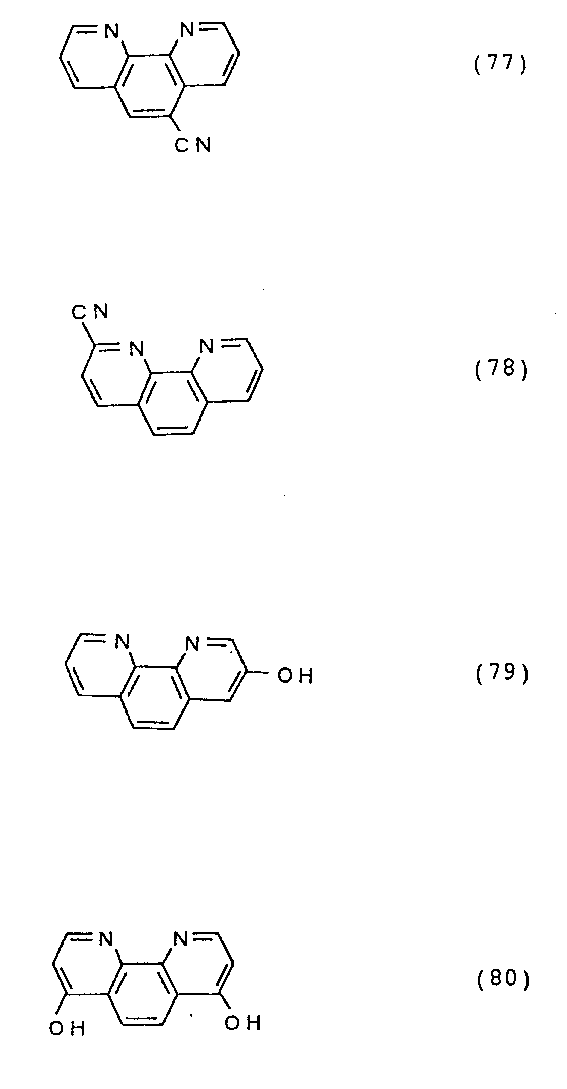
- Preferred examples of 1,10-phenanthroline derivatives which may be employed as the electron transport layer 5 are represented by the following chemical formulas 26 to 82.
- R1 - R8 independently represent a hydrogen atom, a substituted or unsubstituted alkyl group, a substituted or unsubstituted aryl group, a substituted or unsubstituted amino group, a halogen atom, a nitro group, a cyano group or a hydroxyl group.
- R1 - R10 independently represent a hydrogen atom, a substituted or unsubstituted alkyl group, a substituted or unsubstituted aryl group, a substituted or unsubstituted amino group, a halogen atom, a nitro group, a cyano group or a hydroxyl group.
- dihydro-dibenzo-phenanthroline derivatives represented by the following chemical formulas (88) - (91). The present invention is
- a glass substrate on which an anode of ITO had been formed at 1500 ⁇ thick was prepared.
- the substrate was washed by ultrasonic wave for 5 minutes in ethanol.
- the triphenylamine derivative denoted by formula (2) was deposited on the ITO anode at the vacuum deposition rate of 3 ⁇ /sec by using a tantalum boat carrying the derivative to be a hole transport layer with the thickness of 500 ⁇ .
- Each of this this film and the followings were formed by a vacuum deposition method at a vacuum conditions equal to or less than 1.0 ⁇ 10 ⁇ 6 Torr.
- the tetraphenylbutadiene derivative of emitting substance denoted by formula (15) was deposited on the hole transport layer at the vacuum deposition rate of 4 ⁇ /sec to be an emitting layer with the thickness of 200 ⁇ .
- the 1,10-phenanthroline derivative denoted by formula (39) was deposited on the emitting layer at the vacuum deposition rate of 3 ⁇ /sec to be an electron transport layer with the thickness of 500 ⁇ .
- the magnesium and silver alloy was vacuum co-deposited on the electron transport layer in such a manner that magnesium was deposited at the deposition rate of 10 ⁇ /sec simultaneously silver deposited at the deposition rate of 1 ⁇ /sec to be a cathode with the thickness of 1500 ⁇ .
- the emission of this EL device was luminance of 25 cd/m2 of blue light.
- the luminance efficiency was 0.7 lm/W.
- An EL device was assembled by the same procedure as in Example 1, except that the electron transport layer was made of another 1,10-phenanthroline derivative represented by formula (40) instead of the derivative used in Example 1.
- the emission of this EL device was luminance of 47 cd/m2 of blue light.
- the luminance efficiency was 0.3 lm/W.
- An EL device was assembled by the same procedure as in Example 1, except that the emitting layer was made of another tetraphenylbutadiene derivative represented by formula (14) instead of the emitting substance used in Example 1.
- the emission of this EL device was luminance of 72 cd/m2 of blue light.
- the luminance efficiency was 0.4 lm/W.
- An EL device was assembled by the same procedure as in Example 1, except that the emitting layer was made of 1,1,4,4-tetraphenyl-1,3-butadiene represented by formula (16a) instead of the emitting substance used in Example 1.
- the emission of this EL device was luminance of 63 cd/m2 of blue light.
- the luminance efficiency was 1.5 lm/W.
- the emission of this EL device was luminance of 5800 cd/m2 of blue light.
- An EL device was assembled by the same procedure as in Examples 1 and 4, except that the cathode with the thickness of 800 ⁇ was made of aluminum and lithium alloy at the Li concentration 0.2 wt.% in such a manner that the alloy was vacuum co-deposited on the electron transport layer at the deposition rate of 10 ⁇ /sec. instead of the cathode substance used in Example 4.
- the emission of this EL device was luminance of 82 cd/m2 of blue light.
- the luminance efficiency was 2.4 lm/W.
- the emission of this EL device was luminance of 9700 cd/m2 of blue light.
- An EL device was assembled by the same procedure as in Example 1, except that the electron transport layer was not formed between the emitting layer and the cathode.
- the emission of this EL device was luminance of 24 cd/m2 of blue light.
- the luminance efficiency was 0.02 lm/W which was one figure less than that of Example 1.
- An EL device was assembled by the same procedure as in Example 4.
- the resultant EL device was kept by the constant-current application to emit light with luminance of 82 cd/m2 at the same conditions of Example 1t, the half-life of the initial luminance of this EL device was 4 hours and 45 minutes under a vacuum state.
- An EL device was assembled by the same procedure as in Examples 1 and 4, except that the electron transport layer 5 was made of 2-(4'-tert-butylphenyl)-5-(4''-biphenyl)-1,3,4-oxadiazole (so called t-Bu-PBD which is well known as one of superior electron transport materials) denoted by the following chemical formula (86) instead of the electron transport material used in the Example 4.
- the electron transport layer 5 was made of 2-(4'-tert-butylphenyl)-5-(4''-biphenyl)-1,3,4-oxadiazole (so called t-Bu-PBD which is well known as one of superior electron transport materials) denoted by the following chemical formula (86) instead of the electron transport material used in the Example 4.
- the emission of this EL device was luminance of 29 cd/m2 of blue light.
- the luminance efficiency was 1.4 lm/W.
- the emission of this EL device was luminance of 1300 cd/m2.
- the maximum luminance of Comparative 2 was about 1/4 lower than that of Example 4.
- An EL device was assembled by the same procedure as in Examples 1 and 4, except that the electron transport layer was made of another 1,10-phenanthroline derivative represented by formula (40) instead of the derivative used in Example 1.
- the half-life of the initial luminance of this EL device was 4 hours and 45 minutes under a vacuum state.
- the half-life of the initial luminance of this EL device was 35 hours.
- the half-life of the initial luminance of this EL device was 100 hours. The half-life of the initial luminance of this EL device was greatly expanded in comparison with that of Example 2.
- An EL device was assembled by the same procedure as in Examples 1 and 4, except that the electron transport layer was made of 5,6-dihydro-dibenzo[bj]phenanthroline derivative represented by formula (88) instead of the hole transport material used in Example 1.
- the organic EL device comprises the electron hole transport layer, the organic emitting layer and the organic hole transport layer laminated in sequence and arranged between the cathode and the anode, in characterized in that the electron transport layer made of 1,10- or 1,7- or 4,7-phenanthroline derivative or 5,6-dihydro-dibenzo[bj]phenanthroline derivative.
- the organic EL device according to the present invention is capable of improving the durability and to emit blue light at a high luminance and a high efficiency upon application of a low voltage.
Abstract
Description
- The present invention relates to an electroluminescence (EL) device having an emitting layer made of an emitting substance, which utilizes an electroluminescence phenomenon that the emitting substance emits light by applying an electric current to the emitting layer. More particularly, it is concerned with an organic EL device in which the emitting layer is made of an organic emitting substance.
- As organic EL devices, there have been known an device of two-layer structure having two layers of organic compounds as shown in Fig. 1, in which an organic fluorescent thin film 3 (hereinafter referred as "emitting layer") and an organic
hole transport layer 4 are laminated with each other and are arranged between ametal cathode 1 and atransparent anode 2. There have been also known an device of tree-layer structure having three layers of organic compounds as shown in Fig. 2, in which an organicelectron transport layer 5, an emitting layer and an organichole transport layer 4 are laminated in sequence and are sandwiched as a whole between ametal cathode 1 and atransparent anode 2. Thehole transport layer 4 facilitates the infusion of the holes from the anode and blocks electrons. Theelectron transport layer 5 facilitates the infusion of electrons from the cathode. - In these organic EL devices, a
glass substrate 6 is furnished outside thetransparent anode 2. The recombination of electrons infused from themetal cathode 1 and the holes infused from thetransparent anode 2 to the emitting layer 3 generates excitons. The excitons emit light when they are deactivated through radiation. This light radiates toward outside through thetransparent anode 2 and theglass substrate 6. - Such aforementioned organic EL device can emit light even by application of a lower voltage. It is however expected to develop an EL device capable of emission at a further high luminance efficiency.
- An object of the present invention is to provide an organic EL device capable of stably emitting light at a high luminance and a high efficiency to satisfy the above mentioned expectation.
- An organic EL device according to a first aspect of the present invention comprises an anode, a hole transport layer of organic compound, an emitting layer of organic compound, an electron transport layer of organic compound and a cathode, which are laminated in sequence, wherein said electron transport layer is made of a 1,10-phenanthroline derivative represented by the following chemical formula (1a)

where R₁ - R₈ independently represent a hydrogen atom, a substituted or unsubstituted alkyl group, a substituted or unsubstituted aryl group, a substituted or unsubstituted amino group, a halogen atom, a nitro group, a cyano group or a hydroxyl group. - An organic EL device according to a second aspect of the present invention comprises an anode, a hole transport layer of organic compound, an emitting layer of organic compound, an electron transport layer of organic compound and a cathode, which are laminated in sequence, wherein said electron transport layer is made of a 1,7-phenanthroline derivative represented by the following chemical formula (1b)
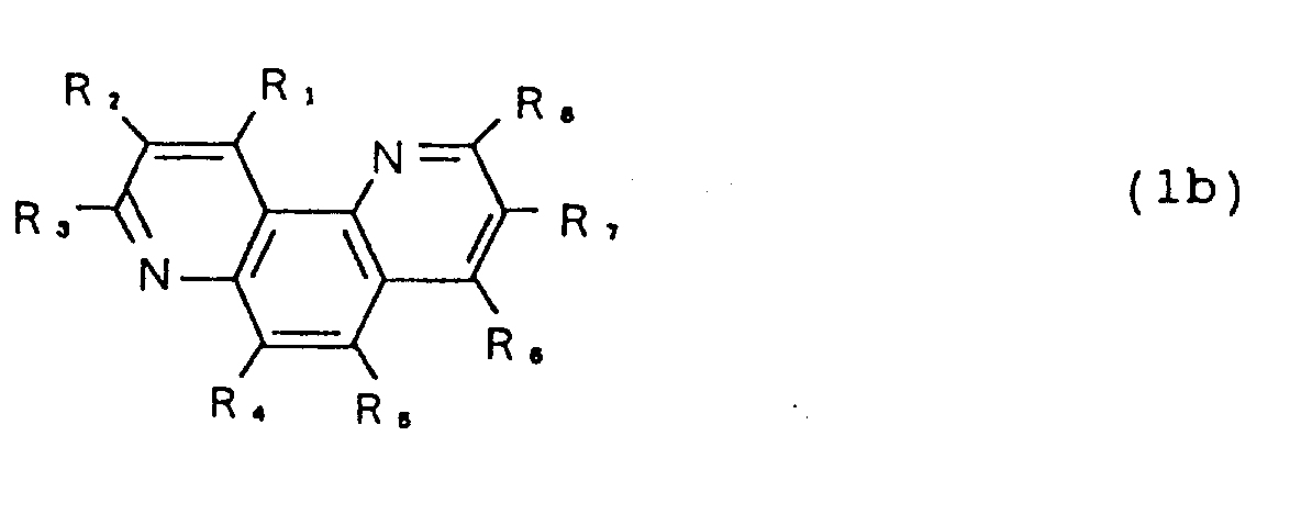
where R₁ - R₈ independently represent a hydrogen atom, a substituted or unsubstituted alkyl group, a substituted or unsubstituted aryl group, a substituted or unsubstituted amino group, a halogen atom, a nitro group, a cyano group or a hydroxyl group. - An organic EL device according to a third aspect of the present invention comprises an anode, a hole transport layer of organic compound, an emitting layer of organic compound, an electron transport layer of organic compound and a cathode, which are laminated in sequence, wherein said electron transport layer is made of a 4,7-phenanthroline derivative represented by the following chemical formula (1c)

where R₁ - R₈ independently represent a hydrogen atom, a substituted or unsubstituted alkyl group, a substituted or unsubstituted aryl group, a substituted or unsubstituted amino group, a halogen atom, a nitro group, a cyano group or a hydroxyl group. - An organic EL device according to a fourth aspect of the present invention comprises an anode, a hole transport layer of organic compound, an emitting layer of organic compound, an electron transport layer of organic compound and a cathode, which are laminated in sequence, wherein said electron transport layer is made of a phenanthroline derivative framed by 5,6-dihydro-dibenzo[bj]phenanthroline represented by the following chemical formula (1d)

where R₁ - R₁₀ independently represent a hydrogen atom, a substituted or unsubstituted alkyl group, a substituted or unsubstituted aryl group, a substituted or unsubstituted amino group, a halogen atom, a nitro group, a cyano group or a hydroxyl group. - According to the present invention, there is obtained an organic EL device capable of stably emitting light at a high luminance and a high efficiency with the durability.
- Fig. 1 is a schematic diagram showing an organic EL device with two-layer structure;
- Fig. 2 is a schematic diagram showing an organic EL device with tree-layer structure; and
- Fig. 3 is a graph showing luminance changes in the lapse of time with respect to organic EL devices of both Example 6 and Comparative 2.
- The embodiments according to the present invention will he described in more detail with reference to the accompanying drawings.
- The EL device in accordance with the present invention is similar to the organic EL device of the structure shown in Fig. 2. Such an EL device has the three-layer structure formed by layering an organic
electron transport layer 5, the organic fluorescent film 3 and the organic positive-hole transport layer 4 in sequence between a pair of themetal cathode 1 and thetransparent anode 2. In this structure of the EL device, at least one of theelectrodes cathode 1 is formed of a metal with a lower work function such as aluminum, magnesium, indium, silver or alloys of the individual metals thereof in the thickness range of from about 100 to 5000 angstroms. Thetransparent anode 2 is formed of an electric conductive material with a higher work function such as indium-tin oxide (ITO) in the thickness range of from about 1000 to 3000 angstroms. Alternatively, thetransparent anode 2 may be formed of gold with the thickness of from about 800 to 1500 angstroms. The electrode of gold thin film is semitransparent. - The
hole transport layer 4 of Fig. 2 is made of a triphenylamine derivative represented by the following formula (2). The organichole transport layer 4 may also be made of a carrier transmitting material (CTM) represented by the following formulas (3) to (13).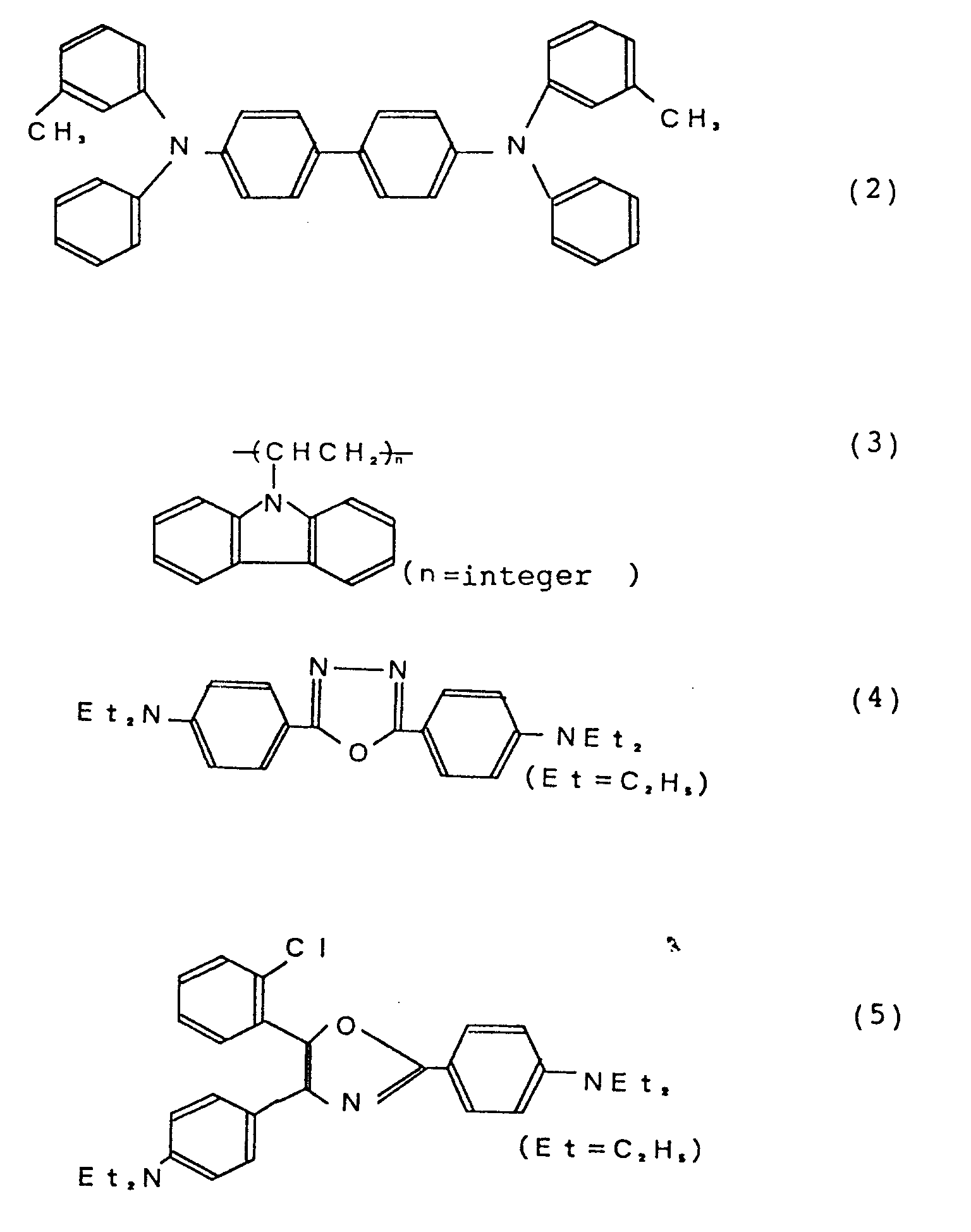


- The emitting layer 3 of the organic EL device comprises the organic fluorescent compound. Preferred examples of the compound are tetraphenylbutadiene (TPB) derivatives respectively represented by the following chemical formulas 14 to 16 and 16a.


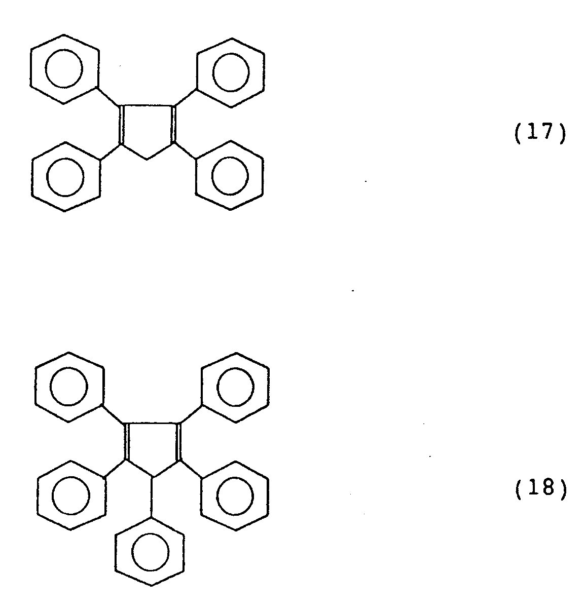
- In addition, other preferred examples used for the emitting layer 3 are represented by the following formulas 17 to 25. The emitting layer 3 may include another fluorescent compound as a guest material. The thickness of the emitting layer 3 is within 1 micron meter or less.


- The
electron transport layer 5 is preferably made of a phenanthroline derivative generally represented by the following chemical formula (1a) which framed by 1,10-phenanthroline hereinafter denoted by formula (26).
where R₁ - R₈ independently represent a hydrogen atom, a substituted or unsubstituted alkyl group, a substituted or unsubstituted aryl group, a substituted or unsubstituted amino group, a halogen atom, a nitro group, a cyano group or a hydroxyl group. - Preferred examples of 1,10-phenanthroline derivatives which may be employed as the
electron transport layer 5 are represented by the following chemical formulas 26 to 82.


- In addition, other preferred examples used for the
electron transport layer 5 are 1,7-phenanthroline derivative represented by the following formula (1b) and 4,7-phenanthroline derivative represented by the following formula (1c).

where R₁ - R₈ independently represent a hydrogen atom, a substituted or unsubstituted alkyl group, a substituted or unsubstituted aryl group, a substituted or unsubstituted amino group, a halogen atom, a nitro group, a cyano group or a hydroxyl group. - Furthermore, another preferred examples used for the
electron transport layer 5 is is made of a phenanthroline derivative framed by 5,6-dihydro-dibenzo[bj]phenanthroline represented by the following chemical formula (1d):
where R₁ - R₁₀ independently represent a hydrogen atom, a substituted or unsubstituted alkyl group, a substituted or unsubstituted aryl group, a substituted or unsubstituted amino group, a halogen atom, a nitro group, a cyano group or a hydroxyl group. Preferred examples of dihydro-dibenzo-phenanthroline derivatives represented by the following chemical formulas (88) - (91). The present invention is not restricted with these examples mentioned above.

- A glass substrate on which an anode of ITO had been formed at 1500Å thick, was prepared. The substrate was washed by ultrasonic wave for 5 minutes in ethanol. After the substrate were dried, the triphenylamine derivative denoted by formula (2) was deposited on the ITO anode at the vacuum deposition rate of 3 Å /sec by using a tantalum boat carrying the derivative to be a hole transport layer with the thickness of 500Å . Each of this this film and the followings were formed by a vacuum deposition method at a vacuum conditions equal to or less than 1.0 × 10⁻⁶ Torr.
- Next, the tetraphenylbutadiene derivative of emitting substance denoted by formula (15) was deposited on the hole transport layer at the vacuum deposition rate of 4 Å /sec to be an emitting layer with the thickness of 200Å .
- Next, the 1,10-phenanthroline derivative denoted by formula (39) was deposited on the emitting layer at the vacuum deposition rate of 3 Å /sec to be an electron transport layer with the thickness of 500Å .
- Then, the magnesium and silver alloy was vacuum co-deposited on the electron transport layer in such a manner that magnesium was deposited at the deposition rate of 10Å /sec simultaneously silver deposited at the deposition rate of 1Å /sec to be a cathode with the thickness of 1500 Å .
- When the resultant EL device was operated with the application of the DC voltage 5V between the ITO anode and the Mg-Ag cathode, the emission of this EL device was luminance of 25 cd/m² of blue light. The luminance efficiency was 0.7 lm/W.
- An EL device was assembled by the same procedure as in Example 1, except that the electron transport layer was made of another 1,10-phenanthroline derivative represented by formula (40) instead of the derivative used in Example 1.
- When the resultant EL device was operated with the application of the DC voltage 12V between the ITO anode and the Mg-Ag cathode, the emission of this EL device was luminance of 47 cd/m² of blue light. The luminance efficiency was 0.3 lm/W.
- An EL device was assembled by the same procedure as in Example 1, except that the emitting layer was made of another tetraphenylbutadiene derivative represented by formula (14) instead of the emitting substance used in Example 1.
- When the resultant EL device was operated with the application of the DC voltage 7V between the ITO anode and the Mg-Ag cathode, the emission of this EL device was luminance of 72 cd/m² of blue light. The luminance efficiency was 0.4 lm/W.
- An EL device was assembled by the same procedure as in Example 1, except that the emitting layer was made of 1,1,4,4-tetraphenyl-1,3-butadiene represented by formula (16a) instead of the emitting substance used in Example 1.
- When the resultant EL device was operated with the application of the DC voltage 6V between the ITO anode and the Mg-Ag cathode, the emission of this EL device was luminance of 63 cd/m² of blue light. The luminance efficiency was 1.5 lm/W. When the resultant EL device was further operated with the application of the DC voltage 13V, the emission of this EL device was luminance of 5800 cd/m² of blue light.
- An EL device was assembled by the same procedure as in Examples 1 and 4, except that the cathode with the thickness of 800Å was made of aluminum and lithium alloy at the Li concentration 0.2 wt.% in such a manner that the alloy was vacuum co-deposited on the electron transport layer at the deposition rate of 10Å /sec. instead of the cathode substance used in Example 4.
- When the resultant EL device was operated with the application of the DC voltage 5V between the ITO anode and the Al-Li cathode, the emission of this EL device was luminance of 82 cd/m² of blue light. The luminance efficiency was 2.4 lm/W. When the resultant EL device was further operated with the application of the DC voltage 12V, the emission of this EL device was luminance of 9700 cd/m² of blue light.
- An EL device was assembled by the same procedure as in Example 1, except that the electron transport layer was not formed between the emitting layer and the cathode.
- When the resultant EL device was operated with the application of the DC voltage 12V between the ITO anode and the Mg-Ag cathode, the emission of this EL device was luminance of 24 cd/m² of blue light. The luminance efficiency was 0.02 lm/W which was one figure less than that of Example 1.
- An EL device was assembled by the same procedure as in Example 4. When the resultant EL device was kept by the constant-current application to emit light with luminance of 82 cd/m² at the same conditions of Example 1t, the half-life of the initial luminance of this EL device was 4 hours and 45 minutes under a vacuum state.
- An EL device was assembled by the same procedure as in Examples 1 and 4, except that the
electron transport layer 5 was made of 2-(4'-tert-butylphenyl)-5-(4''-biphenyl)-1,3,4-oxadiazole (so called t-Bu-PBD which is well known as one of superior electron transport materials) denoted by the following chemical formula (86) instead of the electron transport material used in the Example 4.
- When the resultant EL device was operated with the application of the DC voltage 7V between the ITO anode and the Mg-Ag cathode, the emission of this EL device was luminance of 29 cd/m² of blue light. The luminance efficiency was 1.4 lm/W. When the resultant EL device was further operated with the application of the DC voltage 13V, the emission of this EL device was luminance of 1300 cd/m². The maximum luminance of
Comparative 2 was about 1/4 lower than that of Example 4. - When the resultant EL device was kept by the constant-current application to emit light with luminance of 40 cd/m², the half-life of the initial luminance of this EL device was 4 minutes under a vacuum state, which was far less than that of Example 6 as shown in Fig. 3.
- An EL device was assembled by the same procedure as in Examples 1 and 4, except that the electron transport layer was made of another 1,10-phenanthroline derivative represented by formula (40) instead of the derivative used in Example 1.
- When the resultant EL device was kept by the constant-current application to emit light with luminance of 200 cd/m², the half-life of the initial luminance of this EL device was 4 hours and 45 minutes under a vacuum state. When the initial luminance of 40 cd/m² was kept, the half-life of the initial luminance of this EL device was 35 hours. When the initial luminance of 10 cd/m² was kept, the half-life of the initial luminance of this EL device was 100 hours. The half-life of the initial luminance of this EL device was greatly expanded in comparison with that of Example 2.
- An EL device was assembled by the same procedure as in Examples 1 and 4, except that the electron transport layer was made of 5,6-dihydro-dibenzo[bj]phenanthroline derivative represented by formula (88) instead of the hole transport material used in Example 1.
- When the resultant EL device was kept by the constant-current application to emit light with luminance of 40 cd/m², the half-life of the initial luminance of this EL device was 33 hour, which was greatly expanded in comparison with that of Example 2.
- As described above, the organic EL device according to the present invention comprises the electron hole transport layer, the organic emitting layer and the organic hole transport layer laminated in sequence and arranged between the cathode and the anode, in characterized in that the electron transport layer made of 1,10- or 1,7- or 4,7-phenanthroline derivative or 5,6-dihydro-dibenzo[bj]phenanthroline derivative. The organic EL device according to the present invention is capable of improving the durability and to emit blue light at a high luminance and a high efficiency upon application of a low voltage.
Claims (4)
- An organic Electroluminescence device comprising an anode, a hole transport layer of organic compound, an emitting layer of organic compound, an electron transport layer of organic compound and a cathode, which are laminated in sequence, wherein said electron transport layer is made of a 1,10-phenanthroline derivative represented by the following chemical formula

- An organic Electroluminescence device comprising an anode, a hole transport layer of organic compound, an emitting layer of organic compound, an electron transport layer of organic compound and a cathode, which are laminated in sequence, wherein said electron transport layer is made of a 1,7-phenanthroline derivative represented by the following chemical formula

- An organic Electroluminescence device comprising an anode, a hole transport layer of organic compound, an emitting layer of organic compound, an electron transport layer of organic compound and a cathode, which are laminated in sequence, wherein said electron transport layer is made of a 4,7-phenanthroline derivative represented by the following chemical formula

- An organic Electroluminescence device comprising an anode, a hole transport layer of organic compound, an emitting layer of organic compound, an electron transport layer of organic compound and a cathode, which are laminated in sequence, wherein said electron transport layer is made of a phenanthroline derivative framed by 5,6-dihydro-dibenzo[bj]phenanthroline represented by the following chemical formula

Applications Claiming Priority (4)
| Application Number | Priority Date | Filing Date | Title |
|---|---|---|---|
| JP8219792 | 1992-04-03 | ||
| JP82197/92 | 1992-04-03 | ||
| JP31361892A JP3562652B2 (en) | 1992-04-03 | 1992-11-24 | Organic electroluminescence device |
| JP313618/92 | 1992-11-24 |
Publications (3)
| Publication Number | Publication Date |
|---|---|
| EP0564224A2 true EP0564224A2 (en) | 1993-10-06 |
| EP0564224A3 EP0564224A3 (en) | 1994-01-19 |
| EP0564224B1 EP0564224B1 (en) | 1997-05-28 |
Family
ID=26423213
Family Applications (1)
| Application Number | Title | Priority Date | Filing Date |
|---|---|---|---|
| EP19930302459 Expired - Lifetime EP0564224B1 (en) | 1992-04-03 | 1993-03-30 | Organic electroluminescene device |
Country Status (3)
| Country | Link |
|---|---|
| US (1) | US5393614A (en) |
| EP (1) | EP0564224B1 (en) |
| DE (1) | DE69310982T2 (en) |
Cited By (24)
| Publication number | Priority date | Publication date | Assignee | Title |
|---|---|---|---|---|
| US5650456A (en) * | 1995-02-21 | 1997-07-22 | Bayer Aktiengesellschaft | Coumarin derivatives, a method of preparing them and their use as intermediates |
| US5807945A (en) * | 1995-10-02 | 1998-09-15 | Bayer Ag | (Co)polymers based on vinyl units and use thereof in electroluminescent arrangements |
| US5891975A (en) * | 1995-03-29 | 1999-04-06 | Bayer Aktiengesellschaft | (Co)polymers based on vinyl units and use thereof in electroluminescent devices |
| US5916898A (en) * | 1997-10-24 | 1999-06-29 | Zeneca Limited | Phenanthroline derivatives |
| EP0929104A2 (en) * | 1998-01-09 | 1999-07-14 | Sony Corporation | Electroluminescence device and process for producing the same |
| US6075106A (en) * | 1995-03-29 | 2000-06-13 | D-51368 Bayer Ag | (Co)polymers based on vinyl units and use thereof in electroluminescent devices |
| US6114463A (en) * | 1996-08-16 | 2000-09-05 | Bayer Ag | Copolymers based on vinyl units and their use in electroluminescent devices |
| US6200974B1 (en) | 1997-10-24 | 2001-03-13 | Zeneca Limited | Phenanthroline derivatives |
| EP1097980A2 (en) | 1999-11-02 | 2001-05-09 | Sony Corporation | Bathophenanthroline compound and process for preparing same |
| EP1097981A2 (en) * | 1999-11-02 | 2001-05-09 | Sony Corporation | Organic electroluminescent device |
| US6248457B1 (en) | 1995-02-21 | 2001-06-19 | Bayer Ag | Copolymers based on vinyl units and use thereof in electroluminescent devices |
| WO2002052905A1 (en) | 2000-12-25 | 2002-07-04 | Nec Corporation | Organic electroluminescence element |
| EP1341403A1 (en) * | 2000-11-24 | 2003-09-03 | Toray Industries, Inc. | Luminescent element material and luminescent element comprising the same |
| WO2004005288A2 (en) * | 2002-07-10 | 2004-01-15 | E.I. Du Pont De Nemours And Company | Charge transport compositions comprising fluorinated phenanthroline derivatives |
| WO2004096945A1 (en) * | 2003-05-01 | 2004-11-11 | Fujitsu Limited | 1,3,6,8-tetrasubstituted pyrene compounds, organic el device and organic el display |
| EP2161272A1 (en) | 2008-09-05 | 2010-03-10 | Basf Se | Phenanthrolines |
| EP1786050B1 (en) * | 2005-11-10 | 2010-06-23 | Novaled AG | Doped organic semiconductor material |
| US7750159B2 (en) | 2004-07-07 | 2010-07-06 | Semiconductor Energy Laboratory Co., Ltd. | Phenanthroline derivative and light emitting element and light emitting device using the same |
| CN102372708A (en) * | 2010-08-20 | 2012-03-14 | 清华大学 | Pyridyl phenanthroline compound and application |
| CN102372709A (en) * | 2010-08-20 | 2012-03-14 | 清华大学 | Aryl phenanthroline compound and application thereof |
| US8278651B2 (en) | 2008-12-22 | 2012-10-02 | E I Du Pont De Nemours And Company | Electronic device including 1,7-phenanthroline derivative |
| US8309731B2 (en) | 2008-12-22 | 2012-11-13 | E I Du Pont De Nemours And Company | Electronic device including phenanthroline derivative |
| US9666826B2 (en) | 2005-11-30 | 2017-05-30 | Global Oled Technology Llc | Electroluminescent device including an anthracene derivative |
| CN106866660A (en) * | 2017-02-15 | 2017-06-20 | 上海天马有机发光显示技术有限公司 | Electron transport material, the OLED display panel comprising it and electronic equipment |
Families Citing this family (34)
| Publication number | Priority date | Publication date | Assignee | Title |
|---|---|---|---|---|
| JP3712760B2 (en) * | 1995-05-17 | 2005-11-02 | Tdk株式会社 | Organic EL device |
| JPH1079297A (en) * | 1996-07-09 | 1998-03-24 | Sony Corp | Electroluminescent element |
| KR100277639B1 (en) * | 1998-11-12 | 2001-01-15 | 김순택 | Organic electroluminescent device |
| JP4261855B2 (en) * | 2002-09-19 | 2009-04-30 | キヤノン株式会社 | Phenanthroline compound and organic light emitting device using the same |
| US6713781B1 (en) | 2002-12-04 | 2004-03-30 | Canon Kabushiki Kaisha | Organic light-emitting device having phenanthroline-fused phenazine |
| US7179542B2 (en) | 2003-05-20 | 2007-02-20 | Canon Kabushiki Kaisha | Thiazole- and imidazole-fused phenanthroline molecules in organic light-emitting devices |
| US8188315B2 (en) | 2004-04-02 | 2012-05-29 | Samsung Mobile Display Co., Ltd. | Organic light emitting device and flat panel display device comprising the same |
| EP1783189A4 (en) * | 2004-08-23 | 2009-04-08 | Toray Industries | Material for luminescent element and luminescent element |
| CN101872844B (en) * | 2004-08-23 | 2012-08-08 | 东丽株式会社 | Material for luminous element and luminous element |
| JP2006151866A (en) * | 2004-11-29 | 2006-06-15 | Canon Inc | Phenanthroline compound and light-emitting element |
| US7714501B2 (en) * | 2004-12-01 | 2010-05-11 | Semiconductor Energy Laboratory Co., Ltd. | Light emitting element, light emitting device and electronic equipment |
| JP4612846B2 (en) * | 2005-02-09 | 2011-01-12 | キヤノン株式会社 | Biskinoxaline compound and organic light-emitting device |
| US20060204783A1 (en) * | 2005-03-10 | 2006-09-14 | Conley Scott R | Organic electroluminescent device |
| JP4865258B2 (en) * | 2005-06-21 | 2012-02-01 | キヤノン株式会社 | 1,8-naphthyridine compound and organic light-emitting device using the same |
| US7919010B2 (en) * | 2005-12-22 | 2011-04-05 | Novaled Ag | Doped organic semiconductor material |
| ES2310380T3 (en) * | 2006-03-21 | 2009-01-01 | Novaled Ag | RADICAL OR DIRRADICAL HETEROCICLIC, ITS DIMEROS, OLIGOMEROS, POLYMERS, DIESPIRO COMPOUNDS AND POLICICLOS, ITS USE, ORGANIC SEMICONDUCTOR MATERIAL AS WELL AS ELECTRONIC COMPONENT. |
| EP1837927A1 (en) * | 2006-03-22 | 2007-09-26 | Novaled AG | Use of heterocyclic radicals for doping of organic semiconductors |
| DE102007012794B3 (en) * | 2007-03-16 | 2008-06-19 | Novaled Ag | New pyrido(3,2-h)quinazoline compounds useful to prepare doped organic semi-conductor, which is useful in an organic light-emitting diode, preferably organic solar cells, and modules for an electronic circuits, preferably displays |
| DE102007018456B4 (en) * | 2007-04-19 | 2022-02-24 | Novaled Gmbh | Use of main group element halides and/or pseudohalides, organic semiconducting matrix material, electronic and optoelectronic components |
| EP3076451B1 (en) | 2007-04-30 | 2019-03-06 | Novaled GmbH | Oxocarbon, pseudo oxocarbon and radial compounds and their use |
| EP1990847B1 (en) * | 2007-05-10 | 2018-06-20 | Novaled GmbH | Use of quinoid bisimidazoles and their derivatives as dopant for doping an organic semi-conductor matrix material |
| DE102007031220B4 (en) | 2007-07-04 | 2022-04-28 | Novaled Gmbh | Quinoid compounds and their use in semiconducting matrix materials, electronic and optoelectronic components |
| US7914908B2 (en) * | 2007-11-02 | 2011-03-29 | Global Oled Technology Llc | Organic electroluminescent device having an azatriphenylene derivative |
| US8057712B2 (en) * | 2008-04-29 | 2011-11-15 | Novaled Ag | Radialene compounds and their use |
| US20110037056A1 (en) * | 2008-12-12 | 2011-02-17 | E. I. Du Pont De Nemours And Company | Photoactive composition and electronic device made with the composition |
| US8617720B2 (en) | 2009-12-21 | 2013-12-31 | E I Du Pont De Nemours And Company | Electroactive composition and electronic device made with the composition |
| JP5601064B2 (en) | 2010-07-21 | 2014-10-08 | 富士ゼロックス株式会社 | Photoelectric conversion device, electrophotographic photosensitive member, process cartridge, and image forming apparatus |
| US11168249B1 (en) | 2012-08-29 | 2021-11-09 | Andres Zavaleta Fernandez de Cordova | Luminescent polydentate polycyclic compounds for metal ions |
| US10633586B1 (en) * | 2012-08-29 | 2020-04-28 | Andres Zavaleta Fernandez de Cordova | Luminescent polydentate polycyclic compounds for metal ions |
| TW202339325A (en) | 2013-08-09 | 2023-10-01 | 日商半導體能源研究所股份有限公司 | Light-emitting element, display module, lighting module, light-emitting device, display device, electronic device, and lighting device |
| US9698357B2 (en) | 2014-11-28 | 2017-07-04 | Luminescence Technology Corporation | Phenanthroline-based compound and use thereof |
| KR20170075114A (en) * | 2015-12-22 | 2017-07-03 | 삼성디스플레이 주식회사 | Organic light emitting device |
| KR102579752B1 (en) | 2015-12-22 | 2023-09-19 | 삼성디스플레이 주식회사 | Organic light emitting device |
| KR20170075122A (en) | 2015-12-22 | 2017-07-03 | 삼성디스플레이 주식회사 | Organic light emitting device |
Citations (1)
| Publication number | Priority date | Publication date | Assignee | Title |
|---|---|---|---|---|
| US5077142A (en) * | 1989-04-20 | 1991-12-31 | Ricoh Company, Ltd. | Electroluminescent devices |
Family Cites Families (5)
| Publication number | Priority date | Publication date | Assignee | Title |
|---|---|---|---|---|
| US3654525A (en) * | 1965-10-23 | 1972-04-04 | Donald Leonard Maricle | Electrochemiluminescent device including one of naphthacene, perylene and 5, 6, 11, 12-tetraphenyl-naphthacene in aprotic solvent |
| US3660404A (en) * | 1969-02-24 | 1972-05-02 | Du Pont | U.v.-absorbing ortho-hydroxyphenyl substituted bipyrimidyls |
| JP2879080B2 (en) * | 1989-03-23 | 1999-04-05 | 株式会社リコー | EL device |
| US5128587A (en) * | 1989-12-26 | 1992-07-07 | Moltech Corporation | Electroluminescent device based on organometallic membrane |
| JP3069139B2 (en) * | 1990-03-16 | 2000-07-24 | 旭化成工業株式会社 | Dispersion type electroluminescent device |
-
1993
- 1993-03-26 US US08/037,454 patent/US5393614A/en not_active Expired - Lifetime
- 1993-03-30 EP EP19930302459 patent/EP0564224B1/en not_active Expired - Lifetime
- 1993-03-30 DE DE1993610982 patent/DE69310982T2/en not_active Expired - Lifetime
Patent Citations (1)
| Publication number | Priority date | Publication date | Assignee | Title |
|---|---|---|---|---|
| US5077142A (en) * | 1989-04-20 | 1991-12-31 | Ricoh Company, Ltd. | Electroluminescent devices |
Cited By (49)
| Publication number | Priority date | Publication date | Assignee | Title |
|---|---|---|---|---|
| US6248457B1 (en) | 1995-02-21 | 2001-06-19 | Bayer Ag | Copolymers based on vinyl units and use thereof in electroluminescent devices |
| US5650456A (en) * | 1995-02-21 | 1997-07-22 | Bayer Aktiengesellschaft | Coumarin derivatives, a method of preparing them and their use as intermediates |
| US6403239B2 (en) | 1995-02-21 | 2002-06-11 | Bayer Ag | (Co)polymers based on vinyl units and use thereof in electroluminescent devices |
| US6075106A (en) * | 1995-03-29 | 2000-06-13 | D-51368 Bayer Ag | (Co)polymers based on vinyl units and use thereof in electroluminescent devices |
| US5891975A (en) * | 1995-03-29 | 1999-04-06 | Bayer Aktiengesellschaft | (Co)polymers based on vinyl units and use thereof in electroluminescent devices |
| US5807945A (en) * | 1995-10-02 | 1998-09-15 | Bayer Ag | (Co)polymers based on vinyl units and use thereof in electroluminescent arrangements |
| US5905128A (en) * | 1995-10-02 | 1999-05-18 | Bayer Ag | (CO) polymers based on vinyl units and use thereof in electroluminescent arrangements |
| US6114463A (en) * | 1996-08-16 | 2000-09-05 | Bayer Ag | Copolymers based on vinyl units and their use in electroluminescent devices |
| US6200974B1 (en) | 1997-10-24 | 2001-03-13 | Zeneca Limited | Phenanthroline derivatives |
| US5916898A (en) * | 1997-10-24 | 1999-06-29 | Zeneca Limited | Phenanthroline derivatives |
| EP0929104A3 (en) * | 1998-01-09 | 2003-03-26 | Sony Corporation | Electroluminescence device and process for producing the same |
| EP0929104A2 (en) * | 1998-01-09 | 1999-07-14 | Sony Corporation | Electroluminescence device and process for producing the same |
| US6633122B2 (en) | 1998-01-09 | 2003-10-14 | Sony Corporation | Electroluminescence device with multiple laminated bodies having common materials and process for producing the same |
| EP1097980A2 (en) | 1999-11-02 | 2001-05-09 | Sony Corporation | Bathophenanthroline compound and process for preparing same |
| US6524728B1 (en) * | 1999-11-02 | 2003-02-25 | Sony Corporation | Organic electroluminescent device |
| EP1097981A3 (en) * | 1999-11-02 | 2003-09-24 | Sony Corporation | Organic electroluminescent device |
| EP1097980A3 (en) * | 1999-11-02 | 2003-09-24 | Sony Corporation | Bathophenanthroline compound and process for preparing same |
| EP1097981A2 (en) * | 1999-11-02 | 2001-05-09 | Sony Corporation | Organic electroluminescent device |
| US7186469B2 (en) | 1999-11-02 | 2007-03-06 | Sony Corporation | Bathophenanthroline compound and EL device |
| US6972334B1 (en) | 1999-11-02 | 2005-12-06 | Sony Corporation | Bathophenathroline compound and process for preparing same |
| EP1341403A1 (en) * | 2000-11-24 | 2003-09-03 | Toray Industries, Inc. | Luminescent element material and luminescent element comprising the same |
| EP1341403A4 (en) * | 2000-11-24 | 2007-10-03 | Toray Industries | Luminescent element material and luminescent element comprising the same |
| WO2002052905A1 (en) | 2000-12-25 | 2002-07-04 | Nec Corporation | Organic electroluminescence element |
| EP1365633A1 (en) * | 2000-12-25 | 2003-11-26 | NEC Corporation | Organic electroluminescence element |
| EP2073289A3 (en) * | 2000-12-25 | 2009-11-18 | Samsung Mobile Display Co., Ltd. | Organic electroluminescent device |
| EP1365633A4 (en) * | 2000-12-25 | 2006-11-15 | Samsung Sdi Co Ltd | Organic electroluminescence element |
| US6962995B2 (en) | 2002-07-10 | 2005-11-08 | E. I. Du Pont De Nemours And Company | Charge transport compositions and electronic devices made with such compositions |
| US8293139B2 (en) | 2002-07-10 | 2012-10-23 | E I Du Pont De Nemours And Company | Charge transport compositions and electronic devices made with such compositions |
| WO2004005288A3 (en) * | 2002-07-10 | 2004-06-24 | Du Pont | Charge transport compositions comprising fluorinated phenanthroline derivatives |
| WO2004005288A2 (en) * | 2002-07-10 | 2004-01-15 | E.I. Du Pont De Nemours And Company | Charge transport compositions comprising fluorinated phenanthroline derivatives |
| US8071975B2 (en) | 2002-07-10 | 2011-12-06 | E. I. Du Pont De Nemours And Company | Electronic devices made with electron transport and/or anti-quenching layers |
| US8529796B2 (en) | 2002-07-10 | 2013-09-10 | E I Du Pont De Nemours And Company | Charge transport compositions and electronic devices made with such compositions |
| US7119204B2 (en) | 2002-07-10 | 2006-10-10 | E.I. Du Pont De Nemours And Company | Charge transport compositions and electronic devices made with such compounds |
| US8287769B2 (en) | 2002-07-10 | 2012-10-16 | E I Du Pont De Nemours And Company | Charge transport compositions and electronic devices made with such compositions |
| WO2004096945A1 (en) * | 2003-05-01 | 2004-11-11 | Fujitsu Limited | 1,3,6,8-tetrasubstituted pyrene compounds, organic el device and organic el display |
| US7750159B2 (en) | 2004-07-07 | 2010-07-06 | Semiconductor Energy Laboratory Co., Ltd. | Phenanthroline derivative and light emitting element and light emitting device using the same |
| EP1786050B1 (en) * | 2005-11-10 | 2010-06-23 | Novaled AG | Doped organic semiconductor material |
| US9666826B2 (en) | 2005-11-30 | 2017-05-30 | Global Oled Technology Llc | Electroluminescent device including an anthracene derivative |
| EP2161272A1 (en) | 2008-09-05 | 2010-03-10 | Basf Se | Phenanthrolines |
| US8278651B2 (en) | 2008-12-22 | 2012-10-02 | E I Du Pont De Nemours And Company | Electronic device including 1,7-phenanthroline derivative |
| US8309731B2 (en) | 2008-12-22 | 2012-11-13 | E I Du Pont De Nemours And Company | Electronic device including phenanthroline derivative |
| US8436341B2 (en) | 2008-12-22 | 2013-05-07 | E I Du Pont De Nemours And Company | Electronic device including phenanthroline derivative |
| EP2669967A1 (en) * | 2008-12-22 | 2013-12-04 | E. I. du Pont de Nemours and Company | Electronic device including phenanthroline derivative |
| CN102372708B (en) * | 2010-08-20 | 2013-07-03 | 清华大学 | Pyridyl phenanthroline compound and application |
| CN102372709B (en) * | 2010-08-20 | 2013-08-28 | 清华大学 | Aryl phenanthroline compound and application thereof |
| CN102372709A (en) * | 2010-08-20 | 2012-03-14 | 清华大学 | Aryl phenanthroline compound and application thereof |
| CN102372708A (en) * | 2010-08-20 | 2012-03-14 | 清华大学 | Pyridyl phenanthroline compound and application |
| CN106866660A (en) * | 2017-02-15 | 2017-06-20 | 上海天马有机发光显示技术有限公司 | Electron transport material, the OLED display panel comprising it and electronic equipment |
| CN106866660B (en) * | 2017-02-15 | 2019-05-17 | 上海天马有机发光显示技术有限公司 | Electron transport material, OLED display panel and electronic equipment comprising it |
Also Published As
| Publication number | Publication date |
|---|---|
| EP0564224A3 (en) | 1994-01-19 |
| DE69310982T2 (en) | 1997-11-06 |
| EP0564224B1 (en) | 1997-05-28 |
| US5393614A (en) | 1995-02-28 |
| DE69310982D1 (en) | 1997-07-03 |
Similar Documents
| Publication | Publication Date | Title |
|---|---|---|
| EP0564224B1 (en) | Organic electroluminescene device | |
| JP3562652B2 (en) | Organic electroluminescence device | |
| US5276381A (en) | Organic electroluminescent device | |
| EP0508562B1 (en) | Organic electroluminescence element | |
| EP0562883B1 (en) | Organic electroluminescence device | |
| JP2891783B2 (en) | Organic electroluminescence device | |
| US7291404B2 (en) | Organic light emitting devices | |
| EP0740489B1 (en) | Organic electroluminescent device | |
| US5457565A (en) | Organic electroluminescent device | |
| JP3236332B2 (en) | Organic electroluminescence device | |
| JP2891784B2 (en) | Organic electroluminescence device | |
| JPH05202356A (en) | Organic electroluminescence element | |
| WO2004098242A1 (en) | Light-emitting device | |
| EP1195422B1 (en) | Thin film el device | |
| US5518825A (en) | Organic electroluminescent device | |
| JPH0665569A (en) | Electroluminescent element | |
| JP2000340365A (en) | Organic electroluminescence element | |
| US5346772A (en) | Organic electroluminescence device | |
| JP2000030869A (en) | Organic electroluminescence element | |
| JP3738870B2 (en) | Organic electroluminescence device | |
| JPH06240243A (en) | Organic electroluminescent element | |
| JPH1126164A (en) | Organic electroluminescent element | |
| JPH0790259A (en) | Organic electroluminescence element | |
| JP3241484B2 (en) | Organic electroluminescence device | |
| JPH0978058A (en) | Organic electroluminescent element |
Legal Events
| Date | Code | Title | Description |
|---|---|---|---|
| PUAI | Public reference made under article 153(3) epc to a published international application that has entered the european phase |
Free format text: ORIGINAL CODE: 0009012 |
|
| AK | Designated contracting states |
Kind code of ref document: A2 Designated state(s): DE FR GB NL |
|
| PUAL | Search report despatched |
Free format text: ORIGINAL CODE: 0009013 |
|
| AK | Designated contracting states |
Kind code of ref document: A3 Designated state(s): DE FR GB NL |
|
| 17P | Request for examination filed |
Effective date: 19940330 |
|
| 17Q | First examination report despatched |
Effective date: 19960105 |
|
| GRAG | Despatch of communication of intention to grant |
Free format text: ORIGINAL CODE: EPIDOS AGRA |
|
| GRAH | Despatch of communication of intention to grant a patent |
Free format text: ORIGINAL CODE: EPIDOS IGRA |
|
| RBV | Designated contracting states (corrected) |
Designated state(s): DE |
|
| GRAH | Despatch of communication of intention to grant a patent |
Free format text: ORIGINAL CODE: EPIDOS IGRA |
|
| GRAA | (expected) grant |
Free format text: ORIGINAL CODE: 0009210 |
|
| AK | Designated contracting states |
Kind code of ref document: B1 Designated state(s): DE |
|
| REF | Corresponds to: |
Ref document number: 69310982 Country of ref document: DE Date of ref document: 19970703 |
|
| PLBE | No opposition filed within time limit |
Free format text: ORIGINAL CODE: 0009261 |
|
| STAA | Information on the status of an ep patent application or granted ep patent |
Free format text: STATUS: NO OPPOSITION FILED WITHIN TIME LIMIT |
|
| 26N | No opposition filed | ||
| PGFP | Annual fee paid to national office [announced via postgrant information from national office to epo] |
Ref country code: DE Payment date: 20120411 Year of fee payment: 20 |
|
| REG | Reference to a national code |
Ref country code: DE Ref legal event code: R071 Ref document number: 69310982 Country of ref document: DE |
|
| PG25 | Lapsed in a contracting state [announced via postgrant information from national office to epo] |
Ref country code: DE Free format text: LAPSE BECAUSE OF EXPIRATION OF PROTECTION Effective date: 20130403 |