EP0566929A1 - Method for manufacturing micromechanical structures from monocrystalline semi-conductor material - Google Patents
Method for manufacturing micromechanical structures from monocrystalline semi-conductor material Download PDFInfo
- Publication number
- EP0566929A1 EP0566929A1 EP93105737A EP93105737A EP0566929A1 EP 0566929 A1 EP0566929 A1 EP 0566929A1 EP 93105737 A EP93105737 A EP 93105737A EP 93105737 A EP93105737 A EP 93105737A EP 0566929 A1 EP0566929 A1 EP 0566929A1
- Authority
- EP
- European Patent Office
- Prior art keywords
- saw
- grooves
- silicon
- semiconductor material
- etched
- Prior art date
- Legal status (The legal status is an assumption and is not a legal conclusion. Google has not performed a legal analysis and makes no representation as to the accuracy of the status listed.)
- Ceased
Links
Images

Classifications
-
- G—PHYSICS
- G02—OPTICS
- G02B—OPTICAL ELEMENTS, SYSTEMS OR APPARATUS
- G02B6/00—Light guides; Structural details of arrangements comprising light guides and other optical elements, e.g. couplings
- G02B6/24—Coupling light guides
- G02B6/36—Mechanical coupling means
- G02B6/3628—Mechanical coupling means for mounting fibres to supporting carriers
- G02B6/3684—Mechanical coupling means for mounting fibres to supporting carriers characterised by the manufacturing process of surface profiling of the supporting carrier
- G02B6/3692—Mechanical coupling means for mounting fibres to supporting carriers characterised by the manufacturing process of surface profiling of the supporting carrier with surface micromachining involving etching, e.g. wet or dry etching steps
-
- H—ELECTRICITY
- H01—ELECTRIC ELEMENTS
- H01L—SEMICONDUCTOR DEVICES NOT COVERED BY CLASS H10
- H01L21/00—Processes or apparatus adapted for the manufacture or treatment of semiconductor or solid state devices or of parts thereof
- H01L21/02—Manufacture or treatment of semiconductor devices or of parts thereof
- H01L21/04—Manufacture or treatment of semiconductor devices or of parts thereof the devices having at least one potential-jump barrier or surface barrier, e.g. PN junction, depletion layer or carrier concentration layer
- H01L21/18—Manufacture or treatment of semiconductor devices or of parts thereof the devices having at least one potential-jump barrier or surface barrier, e.g. PN junction, depletion layer or carrier concentration layer the devices having semiconductor bodies comprising elements of Group IV of the Periodic System or AIIIBV compounds with or without impurities, e.g. doping materials
- H01L21/30—Treatment of semiconductor bodies using processes or apparatus not provided for in groups H01L21/20 - H01L21/26
- H01L21/302—Treatment of semiconductor bodies using processes or apparatus not provided for in groups H01L21/20 - H01L21/26 to change their surface-physical characteristics or shape, e.g. etching, polishing, cutting
- H01L21/304—Mechanical treatment, e.g. grinding, polishing, cutting
- H01L21/3043—Making grooves, e.g. cutting
-
- H—ELECTRICITY
- H01—ELECTRIC ELEMENTS
- H01L—SEMICONDUCTOR DEVICES NOT COVERED BY CLASS H10
- H01L21/00—Processes or apparatus adapted for the manufacture or treatment of semiconductor or solid state devices or of parts thereof
- H01L21/02—Manufacture or treatment of semiconductor devices or of parts thereof
- H01L21/04—Manufacture or treatment of semiconductor devices or of parts thereof the devices having at least one potential-jump barrier or surface barrier, e.g. PN junction, depletion layer or carrier concentration layer
- H01L21/18—Manufacture or treatment of semiconductor devices or of parts thereof the devices having at least one potential-jump barrier or surface barrier, e.g. PN junction, depletion layer or carrier concentration layer the devices having semiconductor bodies comprising elements of Group IV of the Periodic System or AIIIBV compounds with or without impurities, e.g. doping materials
- H01L21/30—Treatment of semiconductor bodies using processes or apparatus not provided for in groups H01L21/20 - H01L21/26
- H01L21/302—Treatment of semiconductor bodies using processes or apparatus not provided for in groups H01L21/20 - H01L21/26 to change their surface-physical characteristics or shape, e.g. etching, polishing, cutting
- H01L21/306—Chemical or electrical treatment, e.g. electrolytic etching
- H01L21/30604—Chemical etching
Definitions
- the invention relates to a method for producing micromechanical structures in single-crystal semiconductor material, in which the high accuracy of mask technology and anisotropic etching is used.
- US Pat. No. 4,604,161 describes a method in which saw cuts are used in conjunction with anisotropic etching in order to achieve defined breaking edges in the (111) direction in the case of a silicon wafer.
- a V-groove is created on the active surface of the silicon wafer by structured masking with subsequent anisotropic etching.
- a saw cut is made in the back of the wafer in parallel, but slightly offset from the V-groove.
- a defined break in the (111) direction between the V-groove and the saw cut can now be created by the action of a force.
- a method is also known from US Pat. No. 4,522,682, in which structured masking, saw cuts and anisotropic etching are used in order to produce self-supporting structures, PNP transistors which are dielectrically insulated from the substrate.
- silicon, gallium arsenide or indium phosphide can be used as semiconductor materials.
- Silicon wafers, often as 4 '' wafers, are masked with silicon dioxide and silicon nitride, for example.
- the mask structure specifies the geometries and dimensions of the grooves to be etched.
- the silicon wafers can be anisotropically etched with a highly concentrated potassium hydroxide solution.
- the grooves obtained by this known procedure can now be modified by machining with a precision saw. This can be done both before the etching and after a first etching step and before a second etching step.
- the position and the depth of the saw cut influence and define the geometry of the grooves. Since saw cuts can be made with high precision in silicon, it is possible to produce grooves with a constant cross-section. This enables optical components to be fixed.
- the method according to the invention can be used both with silicon wafers whose surface coincides with a (100) plane and with silicon wafers whose surface coincides with a (110) plane.
- Other single-crystalline semiconductor materials can also be anisotropically etched and processed with a precision saw. The method can be used in the same way for these.
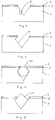
- FIGS. 1 to 11 each show a cross section through a silicon wafer 1, in particular a 4 ′′ wafer made of single-crystal silicon.
- the silicon wafer is provided with a mask, which is composed of a silicon oxide layer 3, for example 50 nm thick, and a silicon nitride layer, for example 140 nm thick.
- the surface of the silicon wafer 1 has masked and unmasked areas 4. If anisotropically etched such a masked silicon wafer 1 with a highly concentrated potassium hydroxide solution, V-shaped grooves 5 are formed in cross section in unmasked area 4 to modify the cross-sectionally V-shaped groove by repeated etching.
- the result is a groove with a diamond cross section 7, the geometry of which can be predetermined by the depth of the saw cut. ( Figures 1 to 4).
- the saw cutting depth and the sawing position must be observed very precisely and can be set, for example, with a precision saw.
- the precision saw used must be suitable for silicon materials. For example, a 40 ⁇ m thick diamond saw blade can be used. If you change the position of the saw cut, the cross section of the groove also changes.
- FIGS. 5 and 6 show a changed position of a saw cut 8 and the groove 9 formed after anisotropic etching.
- the saw cut and the groove symmetry axis do not match.
- the surface of the silicon wafer 1 corresponds to a (100) plane and the bounding edges correspond to the (111) planes which are inclined at 54.7 ° to the (100) plane and are distinguished by the fact that the etching rate perpendicular to these planes is very low compared to the etching rate perpendicular to other crystal planes.
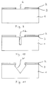
- FIG. 4 shows how an optical waveguide 10, a fiber, can be fixed in the modified groove with a diamond-shaped cross section.
- the groove should be a few centimeters long.
- the fixing properties of such a groove shape are improved compared to that of FIG. 2 by the elimination of a degree of freedom in the vertical direction to the fiber longitudinal axis. It is necessary that the groove cross section does not change over the entire area.
- FIG. 8 shows a movable slide made of silicon 11, on which, for example, an active optical component is mounted, which is movably inserted into a groove.
- Such an arrangement can serve, for example, as an optical switch in an electro-optical module.
- FIGS. 9 to 11 it is assumed that the masked silicon wafer is not etched in the first processing step, but is first provided with a saw cut 12.
- the saw cut is made in an unmasked area 4 of the surface of the silicon wafer 1.
- Anisotropic etching creates a groove 7 ', which then is diamond-shaped if the saw cut 12 has a corresponding saw cut depth.
Landscapes
- Engineering & Computer Science (AREA)
- Physics & Mathematics (AREA)
- General Physics & Mathematics (AREA)
- Computer Hardware Design (AREA)
- Condensed Matter Physics & Semiconductors (AREA)
- Manufacturing & Machinery (AREA)
- Microelectronics & Electronic Packaging (AREA)
- Power Engineering (AREA)
- Optics & Photonics (AREA)
- Chemical & Material Sciences (AREA)
- Chemical Kinetics & Catalysis (AREA)
- General Chemical & Material Sciences (AREA)
- Mechanical Coupling Of Light Guides (AREA)
- Micromachines (AREA)
Abstract
Description
Die Erfindung betrifft ein Verfahren zum Herstellen von mikromechanischen Strukturen in einkristallinem Halbleitermaterial, bei dem die hohe Genauigkeit von Maskentechnik und anisotropem Ätzen ausgenutzt wird.The invention relates to a method for producing micromechanical structures in single-crystal semiconductor material, in which the high accuracy of mask technology and anisotropic etching is used.
Die Reproduzierbarkeit von kristallographischen Winkeln und Ebenen ist aus physikalischen Gründen sehr hoch. Diese Eigenschaften können ausgenutzt werden, um Halterungen für mikrooptische Komponenten und für Lichtwellenleiter herzustellen. Um in einkristallinen Halbleitermaterialien, z.B. Silizium, Fixierungsstrukturen unterschiedlicher Form vorzusehen, ist die alleinige Kombination der Maskentechnik mit anisotropem Ätzen nicht ausreichend. Aus R. Krahn, H. Reichl "Micro System Technologies 91" (Vote-Verlag) "New Microstructures in Silicon using Laser Machining and Anisotropic Etching" von M. Alavi, S. Büttgenbach, A. Schumacher, H.-J. Wagner, Hahn-Schickard-Gesellschaft für angewandte Forschung e.V., W-7000 Stuttgart, 199, S. 322-324, ist es bekannt, mikromechanische Strukturen in Silizium mit Hilfe eines Lasers zu modifizieren. Dazu wird die Oberfläche einer Siliziumscheibe zunächst mit Hilfe der Maskentechnik strukturiert. In einem unmaskierten Bereich der Siliziumscheibe, an einer Stelle, an der eine Nut vorgesehen ist, wird dann mit dem Laser ein Schnitt in der Siliziumscheibe erzeugt. Dadurch werden schnell- und langsam ätzende Kristallebenen freigelegt bzw. beschädigt. Bei einem auf die Laserbearbeitung folgenden anisotropen Ätzprozeß entstehen nun Nuten, die aufgrund des Einschnittes mit dem Laser von ihrer Form her modifiziert sind. So entstehen beispielsweise bei einer Siliziumscheibe, deren Oberfläche mit einer (100)-Ebene des Kristalles zusammenfällt (Bezeichnung der Ebenen mit den Millerschen Indizes), ohne Laserbehandlung V-Nuten und mit Laserbehandlung im Schnitt rautenartige Nuten.The reproducibility of crystallographic angles and planes is very high for physical reasons. These properties can be used to produce holders for micro-optical components and for optical fibers. In order to provide fixing structures of different shapes in single-crystalline semiconductor materials, for example silicon, the mere combination of the mask technique with anisotropic etching is not sufficient. From R. Krahn, H. Reichl "Micro System Technologies 91" (Vote-Verlag) "New Microstructures in Silicon using Laser Machining and Anisotropic Etching" by M. Alavi, S. Büttgenbach, A. Schumacher, H.-J. Wagner, Hahn-Schickard Society for Applied Research eV, W-7000 Stuttgart, 199, pp. 322-324, it is known to modify micromechanical structures in silicon using a laser. To do this, the surface of a silicon wafer is first structured using masking technology. In an unmasked area of the silicon wafer, at a location where a groove is provided, a cut is then made in the silicon wafer with the laser. This quickly and slowly exposes or damages corrosive crystal planes. In the case of an anisotropic etching process following the laser processing, grooves are formed which are modified in shape due to the incision with the laser. For example, with a silicon wafer, the surface of which is formed one (100) -plane of the crystal coincides (designation of the planes with the Miller indices), without laser treatment V-grooves and with laser treatment diamond-shaped grooves on average.
Die Bearbeitung mit einem Laser stellt sich insofern als nachteilig heraus, als es sehr schwierig ist, eine präzise und reproduzierbare Schnittiefe und Position über einen langen Bereich zu erhalten. Variationen der Schnittiefe ergeben jedoch beim anisotropen Ätzen unterschiedliche Nutquerschnitte. Eine genaue Fixierung der optischen Bauelemente ist dann nicht mehr möglich.Processing with a laser turns out to be disadvantageous in that it is very difficult to obtain a precise and reproducible depth of cut and position over a long area. However, variations in the depth of cut result in different groove cross-sections in anisotropic etching. An exact fixation of the optical components is then no longer possible.
In der US 4 604 161 ist ein Verfahren beschrieben, bei dem Sägeschnitte in Verbindung mit anisotropem Ätzen angewendet werden, um bei einer Siliziumscheibe definierte Bruchkanten in (111)-Richtung zu erzielen. Hier wird durch strukturiertes Maskieren mit anschließendem anisotropem Ätzen auf der aktiven Oberfläche der Siliziumscheibe eine V-Nut erzeugt. Im nächsten Schritt wird ein Sägeschnitt in die Rückseite des Wafers parallel, aber etwas versetzt zur V-Nut, ausgeführt. Durch die Einwirkung einer Kraft kann nun eine definierte Bruchstelle in (111)-Richtung zwischen der V-Nut und dem Sägeschnitt erzeugt werden.US Pat. No. 4,604,161 describes a method in which saw cuts are used in conjunction with anisotropic etching in order to achieve defined breaking edges in the (111) direction in the case of a silicon wafer. Here, a V-groove is created on the active surface of the silicon wafer by structured masking with subsequent anisotropic etching. In the next step, a saw cut is made in the back of the wafer in parallel, but slightly offset from the V-groove. A defined break in the (111) direction between the V-groove and the saw cut can now be created by the action of a force.
Aus der US 4 522 682 ist weiterhin ein Verfahren bekannt, bei dem strukturierte Maskierungen, Sägeschnitte und anisotropes Ätzen angewendet werden, um freitragende Strukturen, vom Substrat dielektrisch isolierte PNP-Transistoren, zu erzeugen.A method is also known from US Pat. No. 4,522,682, in which structured masking, saw cuts and anisotropic etching are used in order to produce self-supporting structures, PNP transistors which are dielectrically insulated from the substrate.
Es ist Aufgabe der Erfindung, ein Verfahren zum Herstellen von mikromechanischen Strukturen auf einkristallinen Halbleitermaterialien anzugeben, bei dem geätzte Strukturen mit geringem Aufwand und hoher Präzision modifiziert werden können.It is an object of the invention to provide a method for producing micromechanical structures on single-crystal semiconductor materials, in which etched structures can be modified with little effort and high precision.
Verfahren mit den Merkmalen der Patentansprüche 1 oder 2 lösen diese Aufgabe. Vorteilhafte Weiterbildungen sind in den Unteransprüchen angegeben.Methods with the features of
Als Halbleitermaterialien können insbesondere Silizium, Galliumarsenid oder Indiumphosphid verwendet werden. Siliziumscheiben, oftmals als 4''-Wafer, werden beispielsweise mit Siliziumdioxyd und Siliziumnitrit maskiert. Durch die Maskenstruktur werden Geometrien und Abmessungen der zu ätzenden Nuten vorgegeben. Die Siliziumscheiben können anisotrop mit hochkonzentrierter Kalilauge geätzt werden. Die durch diese bekannte Vorgehensweise erhaltenen Nuten können nun durch Bearbeitung mit einer Präzisionssäge modifiziert werden. Dies kann sowohl vor dem Ätzen als auch nach einem ersten Ätzschritt und vor einem zweiten Ätzschritt erfolgen.In particular, silicon, gallium arsenide or indium phosphide can be used as semiconductor materials. Silicon wafers, often as 4 '' wafers, are masked with silicon dioxide and silicon nitride, for example. The mask structure specifies the geometries and dimensions of the grooves to be etched. The silicon wafers can be anisotropically etched with a highly concentrated potassium hydroxide solution. The grooves obtained by this known procedure can now be modified by machining with a precision saw. This can be done both before the etching and after a first etching step and before a second etching step.
Durch die Lage und die Tiefe des Sägeschnittes wird die Geometrie der Nuten beeinflußt und definiert verändert. Da Sägeschnitte hochgenau in Silizium anbringbar sind, ist es möglich, Nuten mit konstantem Querschnitt herzustellen. Somit wird eine Fixierung von optischen Komponenten ermöglicht.The position and the depth of the saw cut influence and define the geometry of the grooves. Since saw cuts can be made with high precision in silicon, it is possible to produce grooves with a constant cross-section. This enables optical components to be fixed.
Die Anwendung des erfindungsgemäßen Verfahrens ist sowohl bei Siliziumwafern, deren Oberfläche mit einer (100)-Ebene, als auch bei Siliziumwafern, deren Oberfläche mit einer (110)-Ebene zusammenfällt, möglich.The method according to the invention can be used both with silicon wafers whose surface coincides with a (100) plane and with silicon wafers whose surface coincides with a (110) plane.
Andere einkristalline Halbleitermaterialien können ebenfalls anisotrop geätzt und mit einer Präzissionssäge bearbeitet werden. Bei diesen läßt sich das Verfahren in der gleichen Weise anwenden.Other single-crystalline semiconductor materials can also be anisotropically etched and processed with a precision saw. The method can be used in the same way for these.
Ausführungsbeispiele der Erfindung werden anhand der Zeichnungen für das einkristalline Halbleitermaterial Silizium beschrieben. Es zeigen:
Figuren 1 bis 4 einen Schnitt durch eine Siliziumscheibe nach den einzelnen Verfahrensschritten eines Verfahrens nachPatentanspruch 1,Figuren 5 und 6 Schnitte durch eine Siliziumscheibe mit gegenüber denFiguren 3 und 4 veränderter Lage des Sägeschnittes,- Figur 7 Fixierung einer Lichtleitfaser in einer modifizierten Nut,
Figur 8 Fixierung eines beweglichen Schlittens aus Silizium in einer modifizierten Nut und dieFiguren 9 bis 11 Schnitte durch eine Siliziumscheibe nach den einzelnen Verfahrensschritten eines Verfahrens gemäß demPatentanspruch 2.
- 1 to 4 show a section through a silicon wafer after the individual method steps of a method according to
claim 1, - FIGS. 5 and 6 sections through a silicon wafer with a different position of the saw cut compared to FIGS. 3 and 4,
- FIG. 7 fixation of an optical fiber in a modified groove,
- Figure 8 fixation of a movable slide made of silicon in a modified groove and the
- Figures 9 to 11 sections through a silicon wafer after the individual process steps of a method according to
claim 2.
In den Figuren 1 bis 11 ist jeweils ein Querschnitt durch eine Siliziumscheibe 1, insbesondere ein 4''-Wafer aus einkristallinem Silizium, gezeigt. Die Siliziumscheibe ist mit einer Maskierung versehen, die sich zusammensetzt aus einer Siliziumoxydschicht 3, die beispielsweise 50 nm dick ist, und einer Siliziumnitritschicht, die beispielsweise 140 nm dick ist. Die Oberfläche der Siliziumscheibe 1 weist maskierte und unmaskierte Bereiche 4 auf. Wenn man eine so maskierte Siliziumscheibe 1 mit hochkonzentrierter Kalilauge anisotrop ätzt, so entstehen im unmaskierten Bereich 4 im Querschnitt V-förmige Nuten 5. Bringt man im Nutgrund einer solchen V-förmigen Nut einen Sägeschnitt 6 an, der eine bestimmte Sägeschnittstiefe aufweist, so kann man die im Querschnitt V-förmige Nut durch nochmaliges Ätzen modifizieren. Es ergibt sich eine Nut mit einem Rautenquerschnitt 7, deren Geometrie durch die Sägeschnittiefe vorbestimmt werden kann. (Figuren 1 bis 4). Sägeschnittiefe und Sägeposition müssen sehr genau eingehalten werden und sind beispielsweise mit einer Präzisionssäge einstellbar. Die verwendete Präzisionssäge muß für Siliziummaterialien geeignet sein. Beispielsweise kann ein 40 µm dickes Diamantsägeblatt verwendet werden. Wenn man die Lage des Sägeschnittes verändert, so verändert sich auch der Querschnitt der Nut.FIGS. 1 to 11 each show a cross section through a
Die Figuren 5 und 6 zeigen eine geänderte Lage eines Sägeschnittes 8 und die nach anisotropem Ätzen entstandene Nut 9. Hier stimmen Sägeschnitt und Nutsymmetrieachse nicht überein. In den dargestellten Beispielen entspricht die Oberfläche der Siliziumscheibe 1 einer (100)-Ebene und die begrenzenden Flanken entsprechen den (111)-Ebenen, die unter 54,7° zur (100)-Ebene geneigt sind und sich dadurch auszeichnen, daß die Ätzrate senkrecht zu diesen Ebenen im Vergleich zur Ätzrate senkrecht zu anderen Kristallebenen sehr gering ist.FIGS. 5 and 6 show a changed position of a
In Figur 4 ist gezeigt, wie ein Lichtwellenleiter 10, eine Faser, in der modifizierten Nut mit rautenförmigem Querschnitt fixiert werden kann. Die Nut sollte dazu einige Zentimeter lang ausgebildet sein. Die Fixierungseigenschaften einer solchen Nutform sind gegenüber der aus Figur 2 um den Wegfall eines Freiheitsgrades in vertikaler Richtung zur Faserlängsachse verbessert. Es ist dabei notwendig, daß der Nutquerschnitt sich über den gesamten Bereich nicht ändert.FIG. 4 shows how an
Figur 8 zeigt einen beweglichen Schlitten aus Silizium 11, auf dem beispielsweise ein aktives optisches Bauelement montiert wird, der in eine Nut beweglich eingesetzt ist. Eine solche Anordnung kann beispielsweise als optischer Schalter in einem elektrooptischen Modul dienen.FIG. 8 shows a movable slide made of
In den Figuren 9 bis 11 wird davon ausgegangen, daß die maskierte Siliziumscheibe im ersten Bearbeitungsschritt nicht geätzt wird, sondern zunächst mit einem Sägeschnitt 12 versehen wird. Der Sägeschnitt wird in einem unmaskierten Bereich 4 der Oberfläche der Siliziumscheibe 1 angebracht. Durch anisotropes Ätzen entsteht eine Nut 7', die dann rautenförmig ausgebildet ist, wenn der Sägeschnitt 12 eine entsprechende Sägeschnittiefe aufweist.In FIGS. 9 to 11 it is assumed that the masked silicon wafer is not etched in the first processing step, but is first provided with a
Claims (5)
Applications Claiming Priority (2)
| Application Number | Priority Date | Filing Date | Title |
|---|---|---|---|
| DE19924213118 DE4213118C1 (en) | 1992-04-21 | 1992-04-21 | |
| DE4213118 | 1992-04-21 |
Publications (1)
| Publication Number | Publication Date |
|---|---|
| EP0566929A1 true EP0566929A1 (en) | 1993-10-27 |
Family
ID=6457170
Family Applications (1)
| Application Number | Title | Priority Date | Filing Date |
|---|---|---|---|
| EP93105737A Ceased EP0566929A1 (en) | 1992-04-21 | 1993-04-07 | Method for manufacturing micromechanical structures from monocrystalline semi-conductor material |
Country Status (2)
| Country | Link |
|---|---|
| EP (1) | EP0566929A1 (en) |
| DE (1) | DE4213118C1 (en) |
Cited By (3)
| Publication number | Priority date | Publication date | Assignee | Title |
|---|---|---|---|---|
| WO1995016192A1 (en) * | 1993-12-10 | 1995-06-15 | Pharmacia Biotech Ab | Method of producing cavity structures |
| WO1996034305A1 (en) * | 1995-04-27 | 1996-10-31 | Telefonaktiebolaget Lm Ericsson (Publ) | A silicon substrate having a recess for receiving an element, and a method of producing such a recess |
| DE19716480B4 (en) * | 1997-04-19 | 2004-03-25 | Micronas Semiconductor Holding Ag | Method for producing a device with a cavity for receiving an optical waveguide |
Families Citing this family (2)
| Publication number | Priority date | Publication date | Assignee | Title |
|---|---|---|---|---|
| GB2297626A (en) * | 1995-01-27 | 1996-08-07 | Cambridge Consultants | Miniature mounting grooved substrate |
| CN112397616A (en) * | 2020-12-03 | 2021-02-23 | 宣城睿晖宣晟企业管理中心合伙企业(有限合伙) | Cutting method and structure of crystalline silicon battery piece |
Citations (3)
| Publication number | Priority date | Publication date | Assignee | Title |
|---|---|---|---|---|
| GB1246022A (en) * | 1968-09-14 | 1971-09-15 | Hitachi Ltd | Method of manufacturing semiconductor devices |
| US4522682A (en) * | 1982-06-21 | 1985-06-11 | Rockwell International Corporation | Method for producing PNP type lateral transistor separated from substrate by O.D.E. for minimal interference therefrom |
| US4604161A (en) * | 1985-05-02 | 1986-08-05 | Xerox Corporation | Method of fabricating image sensor arrays |
-
1992
- 1992-04-21 DE DE19924213118 patent/DE4213118C1/de not_active Expired - Fee Related
-
1993
- 1993-04-07 EP EP93105737A patent/EP0566929A1/en not_active Ceased
Patent Citations (3)
| Publication number | Priority date | Publication date | Assignee | Title |
|---|---|---|---|---|
| GB1246022A (en) * | 1968-09-14 | 1971-09-15 | Hitachi Ltd | Method of manufacturing semiconductor devices |
| US4522682A (en) * | 1982-06-21 | 1985-06-11 | Rockwell International Corporation | Method for producing PNP type lateral transistor separated from substrate by O.D.E. for minimal interference therefrom |
| US4604161A (en) * | 1985-05-02 | 1986-08-05 | Xerox Corporation | Method of fabricating image sensor arrays |
Non-Patent Citations (1)
| Title |
|---|
| PROCEEDINGS OF THE IEEE Bd. 70, Nr. 5, Mai 1982, NEW YORK US Seiten 420 - 457 K. E. PETERSEN 'Silicon as a mechanical material' paragraphs III and IV * |
Cited By (6)
| Publication number | Priority date | Publication date | Assignee | Title |
|---|---|---|---|---|
| WO1995016192A1 (en) * | 1993-12-10 | 1995-06-15 | Pharmacia Biotech Ab | Method of producing cavity structures |
| US5690841A (en) * | 1993-12-10 | 1997-11-25 | Pharmacia Biotech Ab | Method of producing cavity structures |
| WO1996034305A1 (en) * | 1995-04-27 | 1996-10-31 | Telefonaktiebolaget Lm Ericsson (Publ) | A silicon substrate having a recess for receiving an element, and a method of producing such a recess |
| US6100576A (en) * | 1995-04-27 | 2000-08-08 | Telefonaktiebolaget Lm Ericsson | Silicon substrate having a recess for receiving an element |
| US6482663B1 (en) | 1995-04-27 | 2002-11-19 | Telefonaktiebolaget Lm Ericsson (Publ) | Silicon substrate having a recess for receiving an element, and a method of producing such a recess |
| DE19716480B4 (en) * | 1997-04-19 | 2004-03-25 | Micronas Semiconductor Holding Ag | Method for producing a device with a cavity for receiving an optical waveguide |
Also Published As
| Publication number | Publication date |
|---|---|
| DE4213118C1 (en) | 1993-06-24 |
Similar Documents
| Publication | Publication Date | Title |
|---|---|---|
| EP0631159A1 (en) | Coupling between a planar optical waveguide and an optical fibre and fabrication method for an appropiate planar waveguide | |
| EP0565999A2 (en) | Optical coupling device for two groups of waveguides | |
| DE2303798C2 (en) | Method for manufacturing semiconductor components | |
| DE4429080C1 (en) | Process for the production of prisms, in particular microprisms | |
| EP0012188A1 (en) | Method of manufacturing a fibre-optical separator | |
| EP0286855A1 (en) | Process for etching moats in a silicon substrate | |
| EP2377662A1 (en) | Single crystal | |
| EP0711420B1 (en) | Process of manufacturing a silicon semiconductor substrate with an integrated waveguide coupled to an optical fibre | |
| DE4213118C1 (en) | ||
| EP0509342B1 (en) | Manufacturing process for wedge shaped structures | |
| DE4133885C2 (en) | Three-dimensional silicon structure | |
| DE69930205T2 (en) | Crystal gap device | |
| EP1505383B1 (en) | TEM Probe | |
| EP0538633B1 (en) | Connection between optical fibre and integrated optical waveguide and manufacturing process | |
| DE19743296C1 (en) | Open structure, especially photonic crystal production | |
| DE19526711A1 (en) | Silicon@ wafer mfr. for VLSI mfr. | |
| EP1042794A1 (en) | Process for producing a porous layer by an electrochemical etching process | |
| EP0524179B1 (en) | Process for assembling a wave guide switch | |
| DE2942664C2 (en) | ||
| DE2358881C2 (en) | Process for the production of coupling optics on an optical waveguide | |
| DE112018002065T5 (en) | CHIP PRODUCTION METHOD AND SILICON CHIP | |
| DE19621349C2 (en) | Method for producing three-dimensional structures in a substrate consisting of monocrystalline material with a diamond structure | |
| WO1997031279A1 (en) | Method of producing a master structure | |
| DE4408020B4 (en) | Process for the production of silicon chips with test structures | |
| DE2929186C2 (en) |
Legal Events
| Date | Code | Title | Description |
|---|---|---|---|
| PUAI | Public reference made under article 153(3) epc to a published international application that has entered the european phase |
Free format text: ORIGINAL CODE: 0009012 |
|
| 17P | Request for examination filed |
Effective date: 19930730 |
|
| AK | Designated contracting states |
Kind code of ref document: A1 Designated state(s): DE DK ES FR GB GR IT NL SE |
|
| 17Q | First examination report despatched |
Effective date: 19931201 |
|
| STAA | Information on the status of an ep patent application or granted ep patent |
Free format text: STATUS: THE APPLICATION HAS BEEN REFUSED |
|
| 18R | Application refused |
Effective date: 19951001 |