EP0589268A1 - Integrated optical circuit with a Bragg structure - Google Patents
Integrated optical circuit with a Bragg structure Download PDFInfo
- Publication number
- EP0589268A1 EP0589268A1 EP93114216A EP93114216A EP0589268A1 EP 0589268 A1 EP0589268 A1 EP 0589268A1 EP 93114216 A EP93114216 A EP 93114216A EP 93114216 A EP93114216 A EP 93114216A EP 0589268 A1 EP0589268 A1 EP 0589268A1
- Authority
- EP
- European Patent Office
- Prior art keywords
- waveguide
- integrated optical
- layer
- optical circuit
- carrier plate
- Prior art date
- Legal status (The legal status is an assumption and is not a legal conclusion. Google has not performed a legal analysis and makes no representation as to the accuracy of the status listed.)
- Granted
Links
Images

Classifications
-
- G—PHYSICS
- G02—OPTICS
- G02B—OPTICAL ELEMENTS, SYSTEMS OR APPARATUS
- G02B6/00—Light guides; Structural details of arrangements comprising light guides and other optical elements, e.g. couplings
- G02B6/24—Coupling light guides
- G02B6/26—Optical coupling means
- G02B6/30—Optical coupling means for use between fibre and thin-film device
-
- G—PHYSICS
- G02—OPTICS
- G02B—OPTICAL ELEMENTS, SYSTEMS OR APPARATUS
- G02B6/00—Light guides; Structural details of arrangements comprising light guides and other optical elements, e.g. couplings
- G02B6/10—Light guides; Structural details of arrangements comprising light guides and other optical elements, e.g. couplings of the optical waveguide type
- G02B6/12—Light guides; Structural details of arrangements comprising light guides and other optical elements, e.g. couplings of the optical waveguide type of the integrated circuit kind
- G02B6/122—Basic optical elements, e.g. light-guiding paths
- G02B6/1221—Basic optical elements, e.g. light-guiding paths made from organic materials
-
- G—PHYSICS
- G02—OPTICS
- G02B—OPTICAL ELEMENTS, SYSTEMS OR APPARATUS
- G02B6/00—Light guides; Structural details of arrangements comprising light guides and other optical elements, e.g. couplings
- G02B6/10—Light guides; Structural details of arrangements comprising light guides and other optical elements, e.g. couplings of the optical waveguide type
- G02B6/12—Light guides; Structural details of arrangements comprising light guides and other optical elements, e.g. couplings of the optical waveguide type of the integrated circuit kind
- G02B6/122—Basic optical elements, e.g. light-guiding paths
- G02B6/124—Geodesic lenses or integrated gratings
-
- G—PHYSICS
- G02—OPTICS
- G02B—OPTICAL ELEMENTS, SYSTEMS OR APPARATUS
- G02B6/00—Light guides; Structural details of arrangements comprising light guides and other optical elements, e.g. couplings
- G02B6/10—Light guides; Structural details of arrangements comprising light guides and other optical elements, e.g. couplings of the optical waveguide type
- G02B6/12—Light guides; Structural details of arrangements comprising light guides and other optical elements, e.g. couplings of the optical waveguide type of the integrated circuit kind
- G02B2006/12035—Materials
- G02B2006/12069—Organic material
-
- G—PHYSICS
- G02—OPTICS
- G02B—OPTICAL ELEMENTS, SYSTEMS OR APPARATUS
- G02B6/00—Light guides; Structural details of arrangements comprising light guides and other optical elements, e.g. couplings
- G02B6/10—Light guides; Structural details of arrangements comprising light guides and other optical elements, e.g. couplings of the optical waveguide type
- G02B6/12—Light guides; Structural details of arrangements comprising light guides and other optical elements, e.g. couplings of the optical waveguide type of the integrated circuit kind
- G02B2006/12083—Constructional arrangements
- G02B2006/12107—Grating
-
- G—PHYSICS
- G02—OPTICS
- G02B—OPTICAL ELEMENTS, SYSTEMS OR APPARATUS
- G02B6/00—Light guides; Structural details of arrangements comprising light guides and other optical elements, e.g. couplings
- G02B6/10—Light guides; Structural details of arrangements comprising light guides and other optical elements, e.g. couplings of the optical waveguide type
- G02B6/12—Light guides; Structural details of arrangements comprising light guides and other optical elements, e.g. couplings of the optical waveguide type of the integrated circuit kind
- G02B2006/12133—Functions
- G02B2006/12164—Multiplexing; Demultiplexing
-
- G—PHYSICS
- G02—OPTICS
- G02B—OPTICAL ELEMENTS, SYSTEMS OR APPARATUS
- G02B6/00—Light guides; Structural details of arrangements comprising light guides and other optical elements, e.g. couplings
- G02B6/10—Light guides; Structural details of arrangements comprising light guides and other optical elements, e.g. couplings of the optical waveguide type
- G02B6/12—Light guides; Structural details of arrangements comprising light guides and other optical elements, e.g. couplings of the optical waveguide type of the integrated circuit kind
- G02B2006/12166—Manufacturing methods
- G02B2006/1219—Polymerisation
-
- G—PHYSICS
- G02—OPTICS
- G02B—OPTICAL ELEMENTS, SYSTEMS OR APPARATUS
- G02B6/00—Light guides; Structural details of arrangements comprising light guides and other optical elements, e.g. couplings
- G02B6/10—Light guides; Structural details of arrangements comprising light guides and other optical elements, e.g. couplings of the optical waveguide type
- G02B6/12—Light guides; Structural details of arrangements comprising light guides and other optical elements, e.g. couplings of the optical waveguide type of the integrated circuit kind
- G02B2006/12166—Manufacturing methods
- G02B2006/12195—Tapering
-
- G—PHYSICS
- G02—OPTICS
- G02B—OPTICAL ELEMENTS, SYSTEMS OR APPARATUS
- G02B6/00—Light guides; Structural details of arrangements comprising light guides and other optical elements, e.g. couplings
- G02B6/24—Coupling light guides
- G02B6/36—Mechanical coupling means
- G02B6/3628—Mechanical coupling means for mounting fibres to supporting carriers
- G02B6/3648—Supporting carriers of a microbench type, i.e. with micromachined additional mechanical structures
- G02B6/3652—Supporting carriers of a microbench type, i.e. with micromachined additional mechanical structures the additional structures being prepositioning mounting areas, allowing only movement in one dimension, e.g. grooves, trenches or vias in the microbench surface, i.e. self aligning supporting carriers
-
- G—PHYSICS
- G02—OPTICS
- G02B—OPTICAL ELEMENTS, SYSTEMS OR APPARATUS
- G02B6/00—Light guides; Structural details of arrangements comprising light guides and other optical elements, e.g. couplings
- G02B6/24—Coupling light guides
- G02B6/36—Mechanical coupling means
- G02B6/3628—Mechanical coupling means for mounting fibres to supporting carriers
- G02B6/3684—Mechanical coupling means for mounting fibres to supporting carriers characterised by the manufacturing process of surface profiling of the supporting carrier
- G02B6/3696—Mechanical coupling means for mounting fibres to supporting carriers characterised by the manufacturing process of surface profiling of the supporting carrier by moulding, e.g. injection moulding, casting, embossing, stamping, stenciling, printing, or with metallic mould insert manufacturing using LIGA or MIGA techniques
Landscapes
- Physics & Mathematics (AREA)
- General Physics & Mathematics (AREA)
- Optics & Photonics (AREA)
- Engineering & Computer Science (AREA)
- Microelectronics & Electronic Packaging (AREA)
- Optical Integrated Circuits (AREA)
Abstract
Description
Die Erfindung betrifft eine integriert optische Schaltung mit einer Bragg-Struktur nach der Gattung des Hauptanspruchs und ein Verfahren zu deren Herstellung.The invention relates to an integrated optical circuit with a Bragg structure according to the preamble of the main claim and a method for their production.
Derartige bekannte integriert optische Schaltungen sowie verfahren zu deren Herstellung sind beispielsweise durch Neyer, A. und andere: "New Fabrication Technology for Polymer Optical Waveguides", Integrated Photonics Research, Conference Proceedings, Paper WBZ, 1992, Seiten 248-249) beschrieben. Dabei wird die Struktur im Spritzguß- bzw. Spritzprägeverfahren in die Trägerplatte aus einem Polymer eingeformt. Danach wird die Trägerplatte mit einem Kleber mit höherer Brechzahl versehen und ein Deckel derart aufgepreßt, daß der Kleber die für den Wellenleiter vorgesehene Nut ausfüllt.Known integrated optical circuits of this type and processes for their production are described, for example, by Neyer, A. and others: “New Fabrication Technology for Polymer Optical Waveguides”, Integrated Photonics Research, Conference Proceedings, Paper WBZ, 1992, pages 248-249). The structure is molded into the carrier plate from a polymer using the injection molding or injection molding method. The carrier plate is then provided with an adhesive with a higher refractive index and a cover is pressed on in such a way that the adhesive fills the groove provided for the waveguide.
Sowohl in der Trägerplatte als auch im Deckel befinden sich zum Anschluß von Glasfasern Faserführungsnuten, in welchen Glasfaserenden zur Zuführung bzw. Ableitung der optischen Signale gehalten werden. Durch diese Technik wird u.a. eine verlustarme Ankopplung der Faser an den integriert optischen Wellenleiter durch Anpassung der Wellenleiterparameter (Brechzahl für Mantel und Kern, Wellenleiterquerschnitt) in der polymeren integriert optischen Schaltung an die Wellenleiterparameter der Glasfaser ermöglicht.Both in the carrier plate and in the cover there are fiber guide grooves for connecting glass fibers, in which glass fiber ends are held for supplying or discharging the optical signals. This technology enables low-loss coupling of the fiber to the integrated optical one Waveguide made possible by adapting the waveguide parameters (refractive index for cladding and core, waveguide cross-section) in the polymer integrated optical circuit to the waveguide parameters of the glass fiber.
Sollen in der integriert optischen Schaltung Bragg-Strukturen hergestellt werden, so ergibt sich für die Auslegung der Wellenleiter die Forderung nach einem hohen Koppelwirkungsgrad k zwischen vor- und rücklaufender Welle, was im einzelnen im Buch von Haus, H.: "Waves and Fields in Optoelectronics", Prentice-Hall, 1984, Seite 249 beschrieben ist. Bei einem hohen Koppelwirkungsgrad k haben die Bragg-Strukturen in Längsrichtung des Wellenleiters eine geringe Ausdehnung. Eine Optimierung der Wellenleiterparameter der integriert optischen Schaltung hinsichtlich eines möglichst hohen Koppelwirkungsgrades k ergibt Wellenleiter, deren Feldverteilung erheblich von der Feldverteilung der Glasfaser abweicht. Dadurch erhöhen sich die Koppelverluste bei einfacher Stoßkopplung zwischen Glasfaser und integriert optischem Wellenleiter.If Bragg structures are to be produced in the integrated optical circuit, then there is a requirement for the design of the waveguide for a high coupling efficiency k between the forward and returning wave, which is described in detail in the book by Haus, H .: "Waves and Fields in Optoelectronics ", Prentice-Hall, 1984, page 249. With a high coupling efficiency k, the Bragg structures have a small expansion in the longitudinal direction of the waveguide. An optimization of the waveguide parameters of the integrated optical circuit with regard to a coupling efficiency k that is as high as possible results in waveguides whose field distribution deviates considerably from the field distribution of the glass fiber. This increases the coupling losses with a simple butt coupling between the glass fiber and the integrated optical waveguide.
Optimiert man jedoch die integriert optische Schaltung auf eine gute Feldanpassung an die Glasfaser, ergibt sich ein geringer Koppelwirkungsgrad k und beispielsweise für eine Bragg-Struktur mit etwa 90% Leistungsreflexionsfaktor eine Gesamtlänge in der Größenordnung von Zentimetern, was für den praktischen Einsatz zu lang ist, u.a. deshalb, da sich die geforderte konstante Bragg-Wellenlänge über eine Länge von Zentimetern nur schwierig herstellen läßt. Außerdem ist eine für die Funktion eines derartig langen Bragg-Reflektors notwendige niedrige Wellenleiterdämpfung ebenfalls nur schwer zu realisieren.However, if you optimize the integrated optical circuit for a good field adaptation to the glass fiber, there is a low coupling efficiency k and, for example, for a Bragg structure with about 90% power reflection factor, an overall length of the order of centimeters, which is too long for practical use, among others this is because the required constant Bragg wavelength over a length of centimeters is difficult to produce. In addition, the low waveguide attenuation necessary for the function of such a long Bragg reflector is also difficult to achieve.
Aufgabe der Erfindung ist es, eine integriert optische Schaltung mit hohem Koppelwirkungsgrad k bei gleichzeitiger guter Feldanpassung an die Glasfaser vorzuschlagen, die ohne besondere technologische Schwierigkeiten herstellbar ist.The object of the invention is to propose an integrated optical circuit with a high coupling efficiency k and at the same time good field adaptation to the glass fiber, which without special technological difficulties can be produced.
Die erfindungsgemäße integriert optische Schaltung mit den kennzeichnenden Merkmalen des Hauptanspruchs hat den Vorteil, daß ein hoher Koppelwirkungsgrad k erzielt werden kann, ohne die Feldanpassung an das Feld der Glasfaser zu zerstören. Ein weiterer Vorteil der erfindungsgemäßen Schaltung besteht darin, daß eine Herstellung mit den beispielsweise von Neyer u.a. beschriebenen Technologien möglich ist.The integrated optical circuit according to the invention with the characterizing features of the main claim has the advantage that a high coupling efficiency k can be achieved without destroying the field adaptation to the field of the glass fiber. Another advantage of the circuit according to the invention is that it can be manufactured using the methods described, for example, by Neyer et al. described technologies is possible.
Durch die in den Unteransprüchen aufgeführten Maßnahmen sind vorteilhafte Weiterbildungen und Verbesserungen der im Hauptanspruch angegebenen Erfindung möglich.Advantageous further developments and improvements of the invention specified in the main claim are possible through the measures listed in the subclaims.
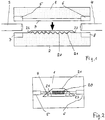
Ausführungsbeispiele der Erfindung sind in der Zeichnung anhand mehrerer Figuren dargestellt und in der nachfolgenden Beschreibung näher erläutert. Es zeigt:
- Fig. 1
- einen Querschnitt durch das Ausführungsbeispiel, wobei die erste und die zweite Trägerplatte noch nicht zusammengesetzt sind,
- Fig. 2
- eine schematische Darstellung des Ausführungsbeispiels,
- Fig. 3 und Fig. 4
- Darstellungen des zum Stand der Technik genannten Verfahrens.
- Fig. 1
- 3 shows a cross section through the exemplary embodiment, the first and second carrier plates not yet being assembled,
- Fig. 2
- 1 shows a schematic representation of the exemplary embodiment,
- 3 and 4
- Representations of the method mentioned in the prior art.
Gleiche Teile sind in den Figuren mit gleichen Bezugszeichen versehen. In Anlehnung an bekannte integriert optische Schaltungen, bei denen eine weitere Platte lediglich als Deckel dient, werden im folgenden die Trägerplatte und die weitere Trägerplatte als Substrat und Deckel bezeichnet. Außerdem stellen die Figuren die Ausführungsbeispiele und die bekannten Schaltungen in einem vergrößerten Maßstab dar.Identical parts are provided with the same reference symbols in the figures. Based on known integrated optical circuits in which a further plate serves only as a cover, the support plate and the further support plate are referred to below as the substrate and cover. In addition, the figures show the exemplary embodiments and the known circuits on an enlarged scale.
Ferner ist in den Figuren 1 und 2 die Bragg-Struktur wesentlich gröber und in Fig. 1 die Dicke der hochbrechenden Schicht übertrieben dargestellt.Furthermore, the Bragg structure is substantially coarser in FIGS. 1 and 2 and the thickness of the high-index layer is exaggerated in FIG. 1.
Das Ausführungsbeispiel nach Fig. 1 besteht aus einem Substrat 1 und einem Deckel 2, die vorzugsweise aus einem Polymer mit einem Brechungsindex bestehen, der demjenigen des Mantels der Glasfasern 3, 4 entspricht. Zur genauen Justierung der Glasfasern 3, 4 sind im Substrat 1 und im Deckel 2 Faserführungsnuten 5, 6, 7, 8 vorgesehen. Im Substrat 1 befindet sich eine Nut 9, welche die beiden Glasfasern 3, 4 miteinander verbindet. Diese Merkmale finden sich auch bei den bekannten integriert optischen Schaltungen, die vor einer weiteren Erläuterung der erfindungsgemäßen Schaltung im folgenden anhand der Figuren 3 und 4 beschrieben werden. Bei der perspektivischen Darstellung in Fig. 3 ist außer dem Substrat 1, den Faserführungsnuten 5, 6 und einer Nut 9 für den Wellenleiter ein Teil 10 einer Spritzgußform aus Metall dargestellt, welches die Negativa für die Faserführungsnuten 15, 16 und die Nut für den Wellenleiter 19 umfaßt, so daß beim Spritzguß die besagte Struktur entsteht.The embodiment according to FIG. 1 consists of a
In einem weiteren Verfahrensschritt wird auf das Substrat ein Kleber aufgebracht, der einen höheren Brechungsindex als das Substrat aufweist und sowohl als Wellenleiter in der Nut 9 als auch zur dauerhaften Verbindung des Substrats mit einem Deckel dient. Dieses ist in Fig. 4 anhand eines Substrats 17 mit drei Nuten 9, 9' und 9'' für Wellenleiter schematisch dargestellt. Die Glasfasern 3, 3', 3'' und 4, 4', 4'' werden zunächst von schematisch dargestellten vorläufigen Halterungen 11, 12 gehalten und in die Faserführungsnuten eingelegt.In a further process step, an adhesive is applied to the substrate, which has a higher refractive index than the substrate and serves both as a waveguide in the
Nach dem Aufbringen des Klebers 13 wird der Deckel 14 auf das Substrat 17 mit großer Andruckkraft aufgepreßt, so daß der Kleber in die Nuten 9, 9', 9'' eindringt und diese ausfüllt. Ferner dringt der Kleber 13 in die nicht von den Glasfasern eingenommenen Teile der Faserführungsnuten ein und fixiert somit die Glasfasern. Der restliche Kleber verteilt sich über die Oberfläche des Substrats 17. Durch entsprechenden Druck wird die Schichtstärke des Klebers möglichst gering gehalten. Nach Aushärten des Klebers ist der Deckel 14 fest mit dem Substrat 17 verbunden.After the application of the
Bei der erfindungsgemäßen Schaltung ist der Deckel 2 (Figuren 1 und 2) mit einer Bragg-Struktur 20 versehen. Dieses kann mit einem geeigneten Abformverfahren erfolgen - beispielsweise durch Spritzguß in einer die Bragg-Struktur aufweisenden Form oder durch Prägen mit einem geeigneten Stempel. Auf die Bragg-Struktur 20 ist eine optische Schicht 21 aufgebracht, deren Brechungsindex über demjenigen des Klebers, also des Wellenleiters, liegt und die deshalb im folgenden als hochbrechende Schicht bezeichnet wird. Ein vorteilhafter Wert des Brechungsindex für die Schicht 21 ist 1,53 bei einem Brechungsindex von 1,48 des Substrats und 1,485 des Wellenleiters.In the circuit according to the invention, the cover 2 (FIGS. 1 and 2) is provided with a Bragg
Ferner sollte die hochbrechende Schicht nur geringe optische Verluste haben und eine Dicke von etwa 0,1µm bis 1µm aufweisen. Bei der Wahl der Schichtdicke und des Brechungsindex der hochbrechenden Schicht ist darauf zu achten, daß der Wellenleiter im Monomodebereich betrieben wird. Dieses ist beispielsweise bei einer Schichtdicke von 0,1µm und einem Brechungsindex von 1,53 der Fall.Furthermore, the high refractive index layer should have only slight optical losses and should have a thickness of approximately 0.1 μm to 1 μm. When choosing the layer thickness and the refractive index of the high-index layer, care must be taken that the waveguide is operated in the single-mode range. This is the case, for example, with a layer thickness of 0.1 µm and a refractive index of 1.53.
Die hochbrechende Schicht 21 erhöht die Wirkung der Bragg-Struktur 20. Dabei sind alle mit Bragg-Strukturen versehenen Flächen mit der hochbrechenden Schicht bedeckt. Zur Vermeidung einer abrupten Stoßstelle im Wellenleiter der integriert optischen Schaltung ist es vorteilhaft, wenn der Wellenleiter vom Faseranschluß her kommend, kontinuierlich in den mit der dünnen hochbrechenden Schicht bedeckten Wellenleiterteil übergeht. Der kontinuierliche Übergang kann durch geeignete Formgebung der hochbrechenden Schicht dadurch erzielt werden, daß die Ränder 22, 23 der hochbrechenden Schicht 21 in Richtung auf die Faserführungsnuten 7, 8 derart verlaufen, daß sie mit dem Wellenleiter einen spitzen Winkel α bilden. Außerdem kann vorgesehen sein, daß die Dicke der hochbrechenden Schicht von den Rändern 22, 23 her allmählich ansteigt.The high-
Bei dem in Fig. 1 dargestellten Ausführungsbeispiel ist die Oberfläche der hochbrechenden Schicht 21 plan, so daß die Dicke der hochbrechenden Schicht 21 entsprechend der Bragg-Struktur wechselt. Dadurch entsteht eine Modulation des Brechungsindex, der auf die im Wellenleiter geführte Lichtwelle wirksam ist. Die Wirkung der Bragg-Struktur wird dadurch weiter erhöht. Eine solche Schicht kann in vorteilhafter Weise durch eine Sprüh-, Tauch- oder Schleuderbeschichtung aufgebracht werden.In the embodiment shown in Fig. 1, the surface of the high-
Es ist im Rahmen der Erfindung jedoch auch möglich, eine gleichmäßig dicke Schicht auf die Bragg-Struktur 20 aufzubringen. Dieses kann beispielsweise durch Plasmaabscheidung, Sputterprozesse oder durch laserunterstützte Chemical Vapour Disposition (Laser-CVD) erfolgen.However, it is also possible within the scope of the invention to apply a uniformly thick layer to the Bragg
Die Wahl dieser Verfahren bleibt dem Fachmann unter Berücksichtigung des jeweils für die hochbrechende Schicht 21 vorgesehenen Werkstoffs überlassen. Als Werkstoffe für die hochbrechende Schicht eignen sich anorganische Dielektrika, wie beispielsweise Al₂O₃, Si₃N₄, SiONH oder siliciumreiches Siliciumnitrid. Ferner kann die hochbrechende Schicht 21 von einem organischen Dielektrikum, insbesondere Polymer, oder einem anorganisch-organischen Polymer (Ormocer) gebildet werden. Diese Werkstoffe eignen sich insbesondere für die Aufbringung nach einem Beschichtungsverfahren im flüssigen Zustand.The choice of these methods is left to the person skilled in the art, taking into account the material provided for the high-
Eine weitere Möglichkeit zur Bildung der hochbrechenden Schicht 21 besteht darin, den Brechungsindex des aus Polymer bestehenden Deckels durch UV-Bestrahlung, Ionendifussions- oder -implantationsverfahren lokal anzuheben. Auch die Diffusion geeigneter Monomeren aus der Gasphase kann den Brechungsindex der polymeren Deckelplatte in der gewünschten Weise anheben. Dabei kann der Deckel selbst dieser Behandlung unterzogen werden oder ein dünner photopolymerisierbarer Film aufgebracht und anschließend durch geeignete Bestrahlung photopolymerisiert werden.Another possibility for forming the high-
Es folgen noch einige Erläuterungen zu den bereits erwähnten Verfahren zur Herstellung der hochbrechenden Schicht:
- 1. Plasmaabscheidung (CVD) dünner Schichten, die beispielsweise als Si₃N₄-Schichten einen Brechungsindex n≈2 oder als nichtstöchiometrische SiOxNyHz-Schichten von der relativen Zusammensetzung (x, y, z)-
abhängige Brechungsindizes 1,46≦n≦2 aufweisen. Durch sogenannte siliciumreiche Siliciumnitridschichten (Herstellung mit Silan und Ammoniakgasen unter geeigneter CVD-Prozeßführung) können Brechungsindizes bis n≈2,6 eingestellt werden. Die Verfahren können durch Anpassung der Plasmaleistung bzw. Kühlung der Substrate so eingestellt werden, daß eine thermische Belastung unterhalb der Glasübergangstemperaturen der Polymerkunststoffe liegt und damit eine Schädigung der eingeprägten Bragg-Strukturen vermieden werden kann. Durch Beschichtungsverfahren in Maskentechnik können die Schichten lateral strukturiert aufgebracht werden (Taperherstellung). - 2. Hochbrechende dielektrische Schichten wie beispielsweise Al₂O₃ (n=1,6) oder Siliciumnitridschichten können durch Sputterprozesse oder auch reaktives Sputtern auf Polymersubstrate aufgebracht werden.
- 3. Laserunterstützte Chemical Vapour Deposition (Laser-CVD) ermöglicht eine schonende lokale Deposition dünner, dielektrischer Schichten auf Polymersubstraten, indem Reaktionsgase wie beispielsweise Silan und Ammoniak über die Probe geführt werden und unter dem Einfluß energiereicher UV-Laserstrahlung lokal an den bestrahlten Probenorten deponiert werden. In diesem Verfahren ist eine ortsaufgelöste Deposition ohne aufwendige Maskentechnik möglich.
- 4. Der Brechungsindex einer Polymerdeckelplatte kann durch eine intensive UV-Bestrahlung, lokale Ionenimplantation oder ganzflächige Überschichtung mit einem polymeren Film, der photopolymerisierbare Oligomere (Photostarter) beinhaltet, und nachfolgende Photopolymerisation lokal angehoben werden. Dadurch ist eine einfache Taperherstellung möglich, wobei die erzielbaren Indexerhöhungen in der Regel gering sind im Vergleich zu
den unter 1.bis 3. genannten Verfahren. - 5. Sprühbeschichtung mit höherbrechenden Dielektrika, die sowohl anorganische Materialien als auch organische Polymere oder auch anorganisch-organische Polymere (sogenannte Ormocere) sein können. Durch automatisierte Sprühverfahren und Verwendung einer Schattenmaske in definiertem Abstand zur Substratoberfläche kann hierbei in besonders vorteilhafter Weise eine lokal begrenzte Fläche beschichtet werden, deren Schichtdicke zum Rand hin allmählich dünner wird (Sprühnebel) und damit ein Tapern der optischen Felder ermöglicht. Die Polymere können üblicherweise auch durch Tauchbeschichtung, durch sogenannte Langmuir-Blodgett Verfahren, oder auch durch Schleuderbeschichtung aufgebracht werden.
- 6. Durch kurzzeitiges Einwirken monomerer oder oligomerer Dämpfe können geeignete organische Stoffe in die Deckelplatte eindiffundiert und dort chemisch gebunden werden. Im Bereich der Diffusionstiefe kann so, abhängig von Materialwahl und eingebrachten Konzentrationen eine Brechungsindexerhöhung eingestellt werden.
- 1. Plasma deposition (CVD) of thin layers, for example as Si₃N₄ layers a refractive index n≈2 or as non-stoichiometric SiO x N y H z layers of the relative composition (x, y, z) -dependent refractive indices 1.46 ≦ n Have ≦ 2. Refractive indices of up to n≈2.6 can be set using so-called silicon-rich silicon nitride layers (production with silane and ammonia gases with suitable CVD process control). The processes can be adjusted by adapting the plasma power or cooling the substrates so that a thermal load is below the glass transition temperatures of the polymer plastics and damage to the impressed Bragg structures can thus be avoided. The layers can be applied in a laterally structured manner using coating methods using mask technology (taper production).
- 2. Highly refractive dielectric layers such as Al₂O₃ (n = 1.6) or silicon nitride layers can be applied to polymer substrates by sputtering processes or reactive sputtering.
- 3. Laser-assisted chemical vapor deposition (laser CVD) enables gentle local deposition of thin, dielectric layers on polymer substrates by passing reaction gases such as silane and ammonia over the sample and depositing them locally at the irradiated sample locations under the influence of high-energy UV laser radiation . In this process, a spatially resolved deposition is possible without complex masking technology.
- 4. The refractive index of a polymer cover plate can be locally increased by intensive UV radiation, local ion implantation or overlap with a polymer film that contains photopolymerizable oligomers (photo starters) and subsequent photopolymerization. This enables simple taper production, the index increases that can be achieved are generally small in comparison to the processes mentioned under 1 to 3.
- 5. Spray coating with higher refractive index dielectrics, which can be both inorganic materials and organic polymers or also inorganic-organic polymers (so-called Ormocere). Automated spraying processes and the use of a shadow mask at a defined distance from the substrate surface can be used in a particularly advantageous manner to coat a locally delimited area, the layer thickness of which gradually becomes thinner towards the edge (spray mist) and thus enables the optical fields to be tapped. The polymers can usually also be applied by dip coating, by what is known as the Langmuir-Blodgett process, or else by spin coating will.
- 6. By brief exposure to monomeric or oligomeric vapors, suitable organic substances can diffuse into the cover plate and be chemically bound there. In the area of the diffusion depth, an increase in the refractive index can be set depending on the choice of material and the concentrations introduced.
Claims (12)
Applications Claiming Priority (2)
| Application Number | Priority Date | Filing Date | Title |
|---|---|---|---|
| DE4231113 | 1992-09-17 | ||
| DE4231113A DE4231113A1 (en) | 1992-09-17 | 1992-09-17 | Integrated optical circuit with a Bragg structure |
Publications (2)
| Publication Number | Publication Date |
|---|---|
| EP0589268A1 true EP0589268A1 (en) | 1994-03-30 |
| EP0589268B1 EP0589268B1 (en) | 1998-04-22 |
Family
ID=6468178
Family Applications (1)
| Application Number | Title | Priority Date | Filing Date |
|---|---|---|---|
| EP93114216A Expired - Lifetime EP0589268B1 (en) | 1992-09-17 | 1993-09-04 | Integrated optical circuit with a Bragg structure |
Country Status (2)
| Country | Link |
|---|---|
| EP (1) | EP0589268B1 (en) |
| DE (2) | DE4231113A1 (en) |
Cited By (6)
| Publication number | Priority date | Publication date | Assignee | Title |
|---|---|---|---|---|
| EP0682276A1 (en) * | 1994-05-12 | 1995-11-15 | Fujitsu Limited | Waveguide-optical fiber connection structure and waveguide-optical fiber connection method |
| EP0807836A2 (en) * | 1996-05-14 | 1997-11-19 | Robert Bosch Gmbh | Method of producing an integrated optical waveguide component and arrangement |
| WO1998058284A1 (en) * | 1997-06-17 | 1998-12-23 | Harting Elektro-Optische Bauteile Gmbh & Co. Kg | Method for producing an integrated optical waveguide component |
| WO2000046620A1 (en) * | 1999-02-04 | 2000-08-10 | INSTITUT FüR MIKROTECHNIK MAINZ GMBH | Lens connector for creating compact optical free-beam systems for several optical fibres |
| EP1182472A2 (en) * | 2000-08-23 | 2002-02-27 | Matsushita Electric Industrial Co., Ltd. | Optical element and method of fabrication thereof |
| JP2002139638A (en) * | 2000-08-23 | 2002-05-17 | Matsushita Electric Ind Co Ltd | Optical element and method for manufacturing the same |
Citations (5)
| Publication number | Priority date | Publication date | Assignee | Title |
|---|---|---|---|---|
| US4636031A (en) * | 1983-10-28 | 1987-01-13 | Chevron Research Company | Process of tuning a grated optical fiber and the tuned optical fiber |
| JPS63106605A (en) * | 1986-10-24 | 1988-05-11 | Hitachi Ltd | Thin film waveguide type optical diffraction element |
| WO1988008548A1 (en) * | 1987-04-28 | 1988-11-03 | British Telecommunications Public Limited Company | Optical device |
| US4923271A (en) * | 1989-03-28 | 1990-05-08 | American Telephone And Telegraph Company | Optical multiplexer/demultiplexer using focusing Bragg reflectors |
| EP0451047A1 (en) * | 1990-04-03 | 1991-10-09 | Commissariat A L'energie Atomique | Environmentally protected integrated optical component and method of manufacturing the same |
-
1992
- 1992-09-17 DE DE4231113A patent/DE4231113A1/en not_active Withdrawn
-
1993
- 1993-09-04 DE DE59308431T patent/DE59308431D1/en not_active Expired - Fee Related
- 1993-09-04 EP EP93114216A patent/EP0589268B1/en not_active Expired - Lifetime
Patent Citations (5)
| Publication number | Priority date | Publication date | Assignee | Title |
|---|---|---|---|---|
| US4636031A (en) * | 1983-10-28 | 1987-01-13 | Chevron Research Company | Process of tuning a grated optical fiber and the tuned optical fiber |
| JPS63106605A (en) * | 1986-10-24 | 1988-05-11 | Hitachi Ltd | Thin film waveguide type optical diffraction element |
| WO1988008548A1 (en) * | 1987-04-28 | 1988-11-03 | British Telecommunications Public Limited Company | Optical device |
| US4923271A (en) * | 1989-03-28 | 1990-05-08 | American Telephone And Telegraph Company | Optical multiplexer/demultiplexer using focusing Bragg reflectors |
| EP0451047A1 (en) * | 1990-04-03 | 1991-10-09 | Commissariat A L'energie Atomique | Environmentally protected integrated optical component and method of manufacturing the same |
Non-Patent Citations (2)
| Title |
|---|
| 'Integrated Photonics Research' A. NEYER et al.: 'New Fabrication Technology for Optical Waveguides' 1992, Conference Proceedings, * |
| PATENT ABSTRACTS OF JAPAN vol. 12, no. 354 (P - 761)<3201> 22 September 1988 (1988-09-22) * |
Cited By (12)
| Publication number | Priority date | Publication date | Assignee | Title |
|---|---|---|---|---|
| EP0682276A1 (en) * | 1994-05-12 | 1995-11-15 | Fujitsu Limited | Waveguide-optical fiber connection structure and waveguide-optical fiber connection method |
| US5557695A (en) * | 1994-05-12 | 1996-09-17 | Fujitsu Limited | Waveguide-optical fiber connection structure and waveguide-optical fiber connection method |
| US5784509A (en) * | 1994-05-12 | 1998-07-21 | Fujitsu Limited | Waveguide-optical fiber connection structure and waveguide-optical fiber connection method |
| EP0940699A1 (en) * | 1994-05-12 | 1999-09-08 | Fujitsu Limited | Waveguide-optical fiber connection structure and waveguide-optical fiber connection method, waveguide substrate for use for waveguide-optical fiber connection and method of producing waveguide substrate as well as optical fiber with fiber substrate for use for waveguide-optical fiber connection |
| EP0807836A2 (en) * | 1996-05-14 | 1997-11-19 | Robert Bosch Gmbh | Method of producing an integrated optical waveguide component and arrangement |
| EP0807836A3 (en) * | 1996-05-14 | 1997-12-17 | Robert Bosch Gmbh | Method of producing an integrated optical waveguide component and arrangement |
| WO1998058284A1 (en) * | 1997-06-17 | 1998-12-23 | Harting Elektro-Optische Bauteile Gmbh & Co. Kg | Method for producing an integrated optical waveguide component |
| WO2000046620A1 (en) * | 1999-02-04 | 2000-08-10 | INSTITUT FüR MIKROTECHNIK MAINZ GMBH | Lens connector for creating compact optical free-beam systems for several optical fibres |
| EP1182472A2 (en) * | 2000-08-23 | 2002-02-27 | Matsushita Electric Industrial Co., Ltd. | Optical element and method of fabrication thereof |
| JP2002139638A (en) * | 2000-08-23 | 2002-05-17 | Matsushita Electric Ind Co Ltd | Optical element and method for manufacturing the same |
| EP1182472A3 (en) * | 2000-08-23 | 2004-02-04 | Matsushita Electric Industrial Co., Ltd. | Optical element and method of fabrication thereof |
| US6826344B2 (en) | 2000-08-23 | 2004-11-30 | Matsushita Electric Industrial Co., Ltd. | Optical element and method of fabrication thereof |
Also Published As
| Publication number | Publication date |
|---|---|
| DE4231113A1 (en) | 1994-03-24 |
| DE59308431D1 (en) | 1998-05-28 |
| EP0589268B1 (en) | 1998-04-22 |
Similar Documents
| Publication | Publication Date | Title |
|---|---|---|
| EP0533074B1 (en) | Method for manufacturing an optical waveguide having an essentially planar substrate | |
| DE4434321C2 (en) | Optical waveguide with a polymer core and its manufacturing process | |
| EP0718418A1 (en) | Process for the production of a graded layer | |
| DE2245374A1 (en) | MULTI-LEVEL INTEGRATED WAVE CONDUCTOR STRUCTURE AND PROCESS FOR THEIR PRODUCTION | |
| DE3520813A1 (en) | METHOD FOR PRODUCING AN INTEGRATED OPTICAL FOCUS | |
| DE19619353A1 (en) | Method for producing an integrated optical waveguide component and arrangement | |
| EP1499490B1 (en) | Method for producing three-dimensional bodies or three-dimensional surfaces by laser radiation | |
| DE3532811C2 (en) | Optical thin film element | |
| DE69926844T2 (en) | Planar lightwave circuit | |
| DE19810584A1 (en) | Method of manufacturing an optical waveguide device | |
| EP0445527B1 (en) | Optical waveguide component and method of manufacturing an optical waveguide component | |
| EP0559040A1 (en) | Process of manufacturing optoelectronic components | |
| EP0589268B1 (en) | Integrated optical circuit with a Bragg structure | |
| EP0883825B1 (en) | Process for the production of optical components with coupled optical waveguides and optical components produced by said method | |
| EP0509342B1 (en) | Manufacturing process for wedge shaped structures | |
| DE2614871C3 (en) | Process for the production of thin-film light guide structures | |
| DE4401219A1 (en) | Integrated optical component and method for producing an integrated optical component | |
| DE2614859A1 (en) | METHOD FOR MANUFACTURING LIGHT GUIDE STRUCTURES WITH INTERMEDIATE ELECTRODES | |
| DE102008038993B4 (en) | Optical element and method for its production | |
| EP0043475A1 (en) | Method of making an integrated micro-optical device to be used with multimode light fibres | |
| DE112004000346T5 (en) | Passive alignment of optical fibers with optical elements | |
| DE3011166A1 (en) | METHOD FOR PRODUCING AN OPTICAL WAVE GUIDE ARRANGEMENT | |
| EP0551118A1 (en) | Method for manufacturing of non-linear micro optical elements | |
| DE60118474T2 (en) | Optical element and method for its production | |
| DE19508025A1 (en) | Method for producing an electro-optical component |
Legal Events
| Date | Code | Title | Description |
|---|---|---|---|
| PUAI | Public reference made under article 153(3) epc to a published international application that has entered the european phase |
Free format text: ORIGINAL CODE: 0009012 |
|
| AK | Designated contracting states |
Kind code of ref document: A1 Designated state(s): DE FR GB IT |
|
| 17P | Request for examination filed |
Effective date: 19940930 |
|
| 17Q | First examination report despatched |
Effective date: 19961018 |
|
| GRAG | Despatch of communication of intention to grant |
Free format text: ORIGINAL CODE: EPIDOS AGRA |
|
| GRAG | Despatch of communication of intention to grant |
Free format text: ORIGINAL CODE: EPIDOS AGRA |
|
| GRAH | Despatch of communication of intention to grant a patent |
Free format text: ORIGINAL CODE: EPIDOS IGRA |
|
| GRAH | Despatch of communication of intention to grant a patent |
Free format text: ORIGINAL CODE: EPIDOS IGRA |
|
| GRAA | (expected) grant |
Free format text: ORIGINAL CODE: 0009210 |
|
| AK | Designated contracting states |
Kind code of ref document: B1 Designated state(s): DE FR GB IT |
|
| ET | Fr: translation filed | ||
| REF | Corresponds to: |
Ref document number: 59308431 Country of ref document: DE Date of ref document: 19980528 |
|
| ITF | It: translation for a ep patent filed |
Owner name: STUDIO JAUMANN P. & C. S.N.C. |
|
| GBT | Gb: translation of ep patent filed (gb section 77(6)(a)/1977) |
Effective date: 19980623 |
|
| PLBE | No opposition filed within time limit |
Free format text: ORIGINAL CODE: 0009261 |
|
| STAA | Information on the status of an ep patent application or granted ep patent |
Free format text: STATUS: NO OPPOSITION FILED WITHIN TIME LIMIT |
|
| 26N | No opposition filed | ||
| REG | Reference to a national code |
Ref country code: GB Ref legal event code: IF02 |
|
| REG | Reference to a national code |
Ref country code: GB Ref legal event code: 732E |
|
| REG | Reference to a national code |
Ref country code: GB Ref legal event code: 732E |
|
| PGFP | Annual fee paid to national office [announced via postgrant information from national office to epo] |
Ref country code: GB Payment date: 20030820 Year of fee payment: 11 |
|
| PGFP | Annual fee paid to national office [announced via postgrant information from national office to epo] |
Ref country code: FR Payment date: 20030909 Year of fee payment: 11 |
|
| PGFP | Annual fee paid to national office [announced via postgrant information from national office to epo] |
Ref country code: DE Payment date: 20030911 Year of fee payment: 11 |
|
| REG | Reference to a national code |
Ref country code: FR Ref legal event code: TP |
|
| PG25 | Lapsed in a contracting state [announced via postgrant information from national office to epo] |
Ref country code: GB Free format text: LAPSE BECAUSE OF NON-PAYMENT OF DUE FEES Effective date: 20040904 |
|
| PG25 | Lapsed in a contracting state [announced via postgrant information from national office to epo] |
Ref country code: DE Free format text: LAPSE BECAUSE OF NON-PAYMENT OF DUE FEES Effective date: 20050401 |
|
| GBPC | Gb: european patent ceased through non-payment of renewal fee |
Effective date: 20040904 |
|
| PG25 | Lapsed in a contracting state [announced via postgrant information from national office to epo] |
Ref country code: FR Free format text: LAPSE BECAUSE OF NON-PAYMENT OF DUE FEES Effective date: 20050531 |
|
| REG | Reference to a national code |
Ref country code: FR Ref legal event code: ST |
|
| PG25 | Lapsed in a contracting state [announced via postgrant information from national office to epo] |
Ref country code: IT Free format text: LAPSE BECAUSE OF NON-PAYMENT OF DUE FEES Effective date: 20050904 |