EP0595583A1 - Non-visualized information recording medium and apparatus for detecting the same - Google Patents
Non-visualized information recording medium and apparatus for detecting the same Download PDFInfo
- Publication number
- EP0595583A1 EP0595583A1 EP93308485A EP93308485A EP0595583A1 EP 0595583 A1 EP0595583 A1 EP 0595583A1 EP 93308485 A EP93308485 A EP 93308485A EP 93308485 A EP93308485 A EP 93308485A EP 0595583 A1 EP0595583 A1 EP 0595583A1
- Authority
- EP
- European Patent Office
- Prior art keywords
- fluorescent
- light
- information
- original document
- reading
- Prior art date
- Legal status (The legal status is an assumption and is not a legal conclusion. Google has not performed a legal analysis and makes no representation as to the accuracy of the status listed.)
- Granted
Links
- 239000000463 material Substances 0.000 claims abstract description 37
- 239000000049 pigment Substances 0.000 claims abstract description 31
- 238000004040 coloring Methods 0.000 claims abstract description 27
- 238000000862 absorption spectrum Methods 0.000 claims abstract description 8
- 230000005764 inhibitory process Effects 0.000 claims description 5
- 230000004304 visual acuity Effects 0.000 claims description 5
- 238000001444 catalytic combustion detection Methods 0.000 description 43
- 238000000034 method Methods 0.000 description 35
- 229910052736 halogen Inorganic materials 0.000 description 32
- 150000002367 halogens Chemical class 0.000 description 32
- 238000001228 spectrum Methods 0.000 description 23
- 238000005520 cutting process Methods 0.000 description 18
- 230000015654 memory Effects 0.000 description 17
- 238000012545 processing Methods 0.000 description 16
- 230000003287 optical effect Effects 0.000 description 15
- 230000008569 process Effects 0.000 description 14
- 230000035945 sensitivity Effects 0.000 description 11
- 238000003705 background correction Methods 0.000 description 10
- 238000001514 detection method Methods 0.000 description 10
- 229910052727 yttrium Inorganic materials 0.000 description 10
- 230000004044 response Effects 0.000 description 9
- 229920005989 resin Polymers 0.000 description 8
- 239000011347 resin Substances 0.000 description 8
- 238000012546 transfer Methods 0.000 description 8
- 238000011161 development Methods 0.000 description 7
- 230000002265 prevention Effects 0.000 description 7
- 150000001875 compounds Chemical class 0.000 description 6
- 238000010586 diagram Methods 0.000 description 6
- 230000002829 reductive effect Effects 0.000 description 6
- 230000003321 amplification Effects 0.000 description 5
- 230000015572 biosynthetic process Effects 0.000 description 5
- 238000006243 chemical reaction Methods 0.000 description 5
- 230000001747 exhibiting effect Effects 0.000 description 5
- 230000005484 gravity Effects 0.000 description 5
- 238000003199 nucleic acid amplification method Methods 0.000 description 5
- 230000000007 visual effect Effects 0.000 description 5
- 238000002835 absorbance Methods 0.000 description 4
- 239000011521 glass Substances 0.000 description 4
- 239000000126 substance Substances 0.000 description 4
- 239000011230 binding agent Substances 0.000 description 3
- 230000000052 comparative effect Effects 0.000 description 3
- 230000000694 effects Effects 0.000 description 3
- 230000000873 masking effect Effects 0.000 description 3
- 229910001507 metal halide Inorganic materials 0.000 description 3
- 150000005309 metal halides Chemical class 0.000 description 3
- 239000007787 solid Substances 0.000 description 3
- JUJWROOIHBZHMG-UHFFFAOYSA-N Pyridine Chemical compound C1=CC=NC=C1 JUJWROOIHBZHMG-UHFFFAOYSA-N 0.000 description 2
- XUIMIQQOPSSXEZ-UHFFFAOYSA-N Silicon Chemical compound [Si] XUIMIQQOPSSXEZ-UHFFFAOYSA-N 0.000 description 2
- 238000003491 array Methods 0.000 description 2
- 239000000969 carrier Substances 0.000 description 2
- 239000003086 colorant Substances 0.000 description 2
- 238000011109 contamination Methods 0.000 description 2
- 239000000835 fiber Substances 0.000 description 2
- 230000006870 function Effects 0.000 description 2
- 230000006872 improvement Effects 0.000 description 2
- 230000001678 irradiating effect Effects 0.000 description 2
- 239000000696 magnetic material Substances 0.000 description 2
- 238000005259 measurement Methods 0.000 description 2
- 229910052710 silicon Inorganic materials 0.000 description 2
- 239000010703 silicon Substances 0.000 description 2
- -1 styryl compound Chemical class 0.000 description 2
- 238000003786 synthesis reaction Methods 0.000 description 2
- 230000002194 synthesizing effect Effects 0.000 description 2
- 230000007704 transition Effects 0.000 description 2
- 229910052724 xenon Inorganic materials 0.000 description 2
- FHNFHKCVQCLJFQ-UHFFFAOYSA-N xenon atom Chemical compound [Xe] FHNFHKCVQCLJFQ-UHFFFAOYSA-N 0.000 description 2
- BCHZICNRHXRCHY-UHFFFAOYSA-N 2h-oxazine Chemical compound N1OC=CC=C1 BCHZICNRHXRCHY-UHFFFAOYSA-N 0.000 description 1
- AGIJRRREJXSQJR-UHFFFAOYSA-N 2h-thiazine Chemical compound N1SC=CC=C1 AGIJRRREJXSQJR-UHFFFAOYSA-N 0.000 description 1
- GZVHEAJQGPRDLQ-UHFFFAOYSA-N 6-phenyl-1,3,5-triazine-2,4-diamine Chemical compound NC1=NC(N)=NC(C=2C=CC=CC=2)=N1 GZVHEAJQGPRDLQ-UHFFFAOYSA-N 0.000 description 1
- GJCOSYZMQJWQCA-UHFFFAOYSA-N 9H-xanthene Chemical compound C1=CC=C2CC3=CC=CC=C3OC2=C1 GJCOSYZMQJWQCA-UHFFFAOYSA-N 0.000 description 1
- 239000004925 Acrylic resin Substances 0.000 description 1
- 229920000178 Acrylic resin Polymers 0.000 description 1
- 229910010092 LiAlO2 Inorganic materials 0.000 description 1
- 229920000877 Melamine resin Polymers 0.000 description 1
- 239000004640 Melamine resin Substances 0.000 description 1
- 229920001807 Urea-formaldehyde Polymers 0.000 description 1
- BZHJMEDXRYGGRV-UHFFFAOYSA-N Vinyl chloride Chemical compound ClC=C BZHJMEDXRYGGRV-UHFFFAOYSA-N 0.000 description 1
- 239000006096 absorbing agent Substances 0.000 description 1
- 238000010521 absorption reaction Methods 0.000 description 1
- 229920000180 alkyd Polymers 0.000 description 1
- 230000008859 change Effects 0.000 description 1
- 238000010276 construction Methods 0.000 description 1
- 229920001577 copolymer Polymers 0.000 description 1
- 238000012937 correction Methods 0.000 description 1
- 230000003247 decreasing effect Effects 0.000 description 1
- 230000003111 delayed effect Effects 0.000 description 1
- 238000012217 deletion Methods 0.000 description 1
- 230000037430 deletion Effects 0.000 description 1
- 238000000151 deposition Methods 0.000 description 1
- 239000006185 dispersion Substances 0.000 description 1
- 238000009826 distribution Methods 0.000 description 1
- 230000008030 elimination Effects 0.000 description 1
- 238000003379 elimination reaction Methods 0.000 description 1
- 238000010556 emulsion polymerization method Methods 0.000 description 1
- 238000001093 holography Methods 0.000 description 1
- 238000003384 imaging method Methods 0.000 description 1
- 230000006698 induction Effects 0.000 description 1
- 239000003112 inhibitor Substances 0.000 description 1
- 230000002401 inhibitory effect Effects 0.000 description 1
- 150000002484 inorganic compounds Chemical class 0.000 description 1
- 229910010272 inorganic material Inorganic materials 0.000 description 1
- QDLAGTHXVHQKRE-UHFFFAOYSA-N lichenxanthone Natural products COC1=CC(O)=C2C(=O)C3=C(C)C=C(OC)C=C3OC2=C1 QDLAGTHXVHQKRE-UHFFFAOYSA-N 0.000 description 1
- 238000002156 mixing Methods 0.000 description 1
- 230000003647 oxidation Effects 0.000 description 1
- 238000007254 oxidation reaction Methods 0.000 description 1
- 238000010422 painting Methods 0.000 description 1
- 238000010298 pulverizing process Methods 0.000 description 1
- UMJSCPRVCHMLSP-UHFFFAOYSA-N pyridine Natural products COC1=CC=CN=C1 UMJSCPRVCHMLSP-UHFFFAOYSA-N 0.000 description 1
- 238000006862 quantum yield reaction Methods 0.000 description 1
- 229910052761 rare earth metal Inorganic materials 0.000 description 1
- 238000005070 sampling Methods 0.000 description 1
- 239000004065 semiconductor Substances 0.000 description 1
- 229940124530 sulfonamide Drugs 0.000 description 1
- 239000012463 white pigment Substances 0.000 description 1
Images


Classifications
-
- H—ELECTRICITY
- H04—ELECTRIC COMMUNICATION TECHNIQUE
- H04N—PICTORIAL COMMUNICATION, e.g. TELEVISION
- H04N1/00—Scanning, transmission or reproduction of documents or the like, e.g. facsimile transmission; Details thereof
- H04N1/00838—Preventing unauthorised reproduction
- H04N1/0084—Determining the necessity for prevention
- H04N1/00843—Determining the necessity for prevention based on recognising a copy prohibited original, e.g. a banknote
- H04N1/00846—Determining the necessity for prevention based on recognising a copy prohibited original, e.g. a banknote based on detection of a dedicated indication, e.g. marks or the like
-
- B—PERFORMING OPERATIONS; TRANSPORTING
- B41—PRINTING; LINING MACHINES; TYPEWRITERS; STAMPS
- B41M—PRINTING, DUPLICATING, MARKING, OR COPYING PROCESSES; COLOUR PRINTING
- B41M3/00—Printing processes to produce particular kinds of printed work, e.g. patterns
- B41M3/14—Security printing
- B41M3/144—Security printing using fluorescent, luminescent or iridescent effects
-
- B—PERFORMING OPERATIONS; TRANSPORTING
- B42—BOOKBINDING; ALBUMS; FILES; SPECIAL PRINTED MATTER
- B42D—BOOKS; BOOK COVERS; LOOSE LEAVES; PRINTED MATTER CHARACTERISED BY IDENTIFICATION OR SECURITY FEATURES; PRINTED MATTER OF SPECIAL FORMAT OR STYLE NOT OTHERWISE PROVIDED FOR; DEVICES FOR USE THEREWITH AND NOT OTHERWISE PROVIDED FOR; MOVABLE-STRIP WRITING OR READING APPARATUS
- B42D25/00—Information-bearing cards or sheet-like structures characterised by identification or security features; Manufacture thereof
- B42D25/20—Information-bearing cards or sheet-like structures characterised by identification or security features; Manufacture thereof characterised by a particular use or purpose
- B42D25/29—Securities; Bank notes
-
- G—PHYSICS
- G03—PHOTOGRAPHY; CINEMATOGRAPHY; ANALOGOUS TECHNIQUES USING WAVES OTHER THAN OPTICAL WAVES; ELECTROGRAPHY; HOLOGRAPHY
- G03G—ELECTROGRAPHY; ELECTROPHOTOGRAPHY; MAGNETOGRAPHY
- G03G21/00—Arrangements not provided for by groups G03G13/00 - G03G19/00, e.g. cleaning, elimination of residual charge
- G03G21/04—Preventing copies being made of an original
- G03G21/046—Preventing copies being made of an original by discriminating a special original, e.g. a bank note
-
- G—PHYSICS
- G07—CHECKING-DEVICES
- G07D—HANDLING OF COINS OR VALUABLE PAPERS, e.g. TESTING, SORTING BY DENOMINATIONS, COUNTING, DISPENSING, CHANGING OR DEPOSITING
- G07D7/00—Testing specially adapted to determine the identity or genuineness of valuable papers or for segregating those which are unacceptable, e.g. banknotes that are alien to a currency
- G07D7/06—Testing specially adapted to determine the identity or genuineness of valuable papers or for segregating those which are unacceptable, e.g. banknotes that are alien to a currency using wave or particle radiation
- G07D7/12—Visible light, infrared or ultraviolet radiation
- G07D7/121—Apparatus characterised by sensor details
-
- H—ELECTRICITY
- H04—ELECTRIC COMMUNICATION TECHNIQUE
- H04N—PICTORIAL COMMUNICATION, e.g. TELEVISION
- H04N1/00—Scanning, transmission or reproduction of documents or the like, e.g. facsimile transmission; Details thereof
- H04N1/00838—Preventing unauthorised reproduction
- H04N1/00856—Preventive measures
- H04N1/00864—Modifying the reproduction, e.g. outputting a modified copy of a scanned original
- H04N1/00867—Modifying the reproduction, e.g. outputting a modified copy of a scanned original with additional data, e.g. by adding a warning message
-
- H—ELECTRICITY
- H04—ELECTRIC COMMUNICATION TECHNIQUE
- H04N—PICTORIAL COMMUNICATION, e.g. TELEVISION
- H04N1/00—Scanning, transmission or reproduction of documents or the like, e.g. facsimile transmission; Details thereof
- H04N1/00838—Preventing unauthorised reproduction
- H04N1/00856—Preventive measures
- H04N1/00875—Inhibiting reproduction, e.g. by disabling reading or reproduction apparatus
-
- H—ELECTRICITY
- H04—ELECTRIC COMMUNICATION TECHNIQUE
- H04N—PICTORIAL COMMUNICATION, e.g. TELEVISION
- H04N1/00—Scanning, transmission or reproduction of documents or the like, e.g. facsimile transmission; Details thereof
- H04N1/00838—Preventing unauthorised reproduction
- H04N1/00883—Auto-copy-preventive originals, i.e. originals that are designed not to allow faithful reproduction
Abstract
Description
- The present invention relates to a medium, on which non-visualized information has been recorded, and an apparatus for detecting and making use of the same.
- In recent years there is a great risk of copying images, copying of which is inhibited, in the trend of improvement in the performance of copying machines and the like. Therefore, there is a necessity of discriminating whether or not the subject image is made by copying. Further, the foregoing copying operation must be detected to previously prevent such copying. At present, there have been suggested the following counterfeit prevention methods: a marking method using ultraviolet pigment of a type excited by ultraviolet rays, a method using a diffraction phenomenon such as holography, a method in which a magnetic material is applied as to be detected by a magnetic head, a method using color change by means of photo-chromism and a method in which a specific image is distinguished by means of image recognition.
- However, the method using the ultraviolet pigment of the type excited by ultraviolet encounters a problem that a countermeasure can be taken because the ultraviolet pigment can easily be detected by an ultraviolet-ray emitting means, such as a black lamp. Further, a necessity of providing an exclusive ultraviolet-ray light source makes the optical system to be complicated. The method using the diffraction phenomenon such as hologram has a problem that the cost cannot be reduced because a mark must be formed on the original. The method, in which the magnetic material is applied, involves a necessity of bringing the original into contact with the magnetic head in a hermetic manner. Therefore, a problem arises in this case that the apparatus structure becomes too complicated. The method using the photo-chromism suffers from a problem in that the photo-chromism compound is unstable. The image recognition method must be a great quantity of data to recognize all original documents, resulting in the heavy apparatus load and impossibility in cutting the cost.
- In order to overcome the foregoing problems, a method using near infrared fluorescent light has been suggested which enables a light emission diode exhibiting a long life to be used, resulting in that the influence of contamination can be eliminated (see Japanese Patent Laid-Open Appln. No. 51-88300). However, a light emission diode or a photo-diode capable of sensing long wave lengths must be used, causing a problem to arise in that the apparatus structure becomes too complicated.
- Accordingly, an object of the present invention is to provide a mark having non-visualized information recorded thereon and an apparatus for detecting and using the mark with which specific images can be cheaply and assuredly discriminated.
- In order to achieve the foregoing object, according to an aspect of the present invention, there is provided a non-visualized information recording medium comprising: an identification mark formed by an ink containing a plurality of fluorescent coloring materials or fluorescent pigments, each of which has a fluorescent wave length in a near infrared region, and which have absorption spectrums having the maximum wave lengths that do not overlap each other.
- According to another aspect of the present invention, there is provided an apparatus for judging a specific document comprising: reading means for reading fluorescent information except for visible light information from an original document on which an identification mark formed by an ink containing a plurality of fluorescent coloring materials or fluorescent pigments, each of which has a fluorescent wave length in a near infrared region, and which have absorption spectrums having the maximum wave lengths that do not overlap each other; and judging means for judging whether or not the original document read by the reading means is a specific document.
- By using a plurality of fluorescent materials or the pigments having the substantially the same fluorescent wave lengths in the near infrared region and having the different absorption wave lengths as the mark formed by the recorded non-visualized information as described above, the mark can be reproduced and utilized by using a light source, such as a halogen lamp, a metal halide lamp, a xenon lamp or a fluorescent lamp, having continued spectrum or a plurality of bright lines in a range from the visual region to the infrared region while preventing a visual detection.
- Other and further objects, features and advantages of the invention will be apparent more fully from the following description.
-
- Fig. 1 illustrates a state where an identification mark of a copy-inhibited original document is detected according to a second embodiment of the present invention;
- Fig. 2 is a structural view which illustrates a color copying apparatus embodying the present invention;
- Fig. 3 illustrates an operation of detecting the copy-inhibited original document according to the second embodiment of the present invention;
- Fig. 4 is a comprised of Figs. 4A and 4B showing structural views which illustrate a signal processing portion according to the second embodiment of the present invention;
- Fig. 5 is a graph which shows the timing of each of image control signals according to second to fourth embodiments of the present invention;
- Fig. 6 is a block diagram which illustrates a noise eliminating block of a fluorescent signal according to the second embodiment of the present invention;
- Fig. 7 is comprised of Figs. 7A and 7B showing block diagrams which illustrate a section for detecting the position of a fluorescent mark according to the second embodiment of the present invention;
- Fig. 8 is a portion for generating address in a memory for storing the fluorescent mark according to the second embodiment of the present invention;
- Fig. 9 is a flow chart which illustrates control performed by a CPU according to the second embodiment of the present invention;
- Fig. 10 is a flow chart which illustrates a pattern matching operation performed by the CPU according to the second embodiment of the present invention;
- Fig. 11 illustrates an operation of thinning the fluorescent mark according to the second embodiment of the present invention;
- Figs. 12A, 12B and 12C are schematic views which illustrate the fluorescent pattern matching operation according to the second embodiment of the present invention;
- Fig. 13 illustrates spectrum characteristics of a filter disposed in the immediately rear of an original document irradiation lamp according to the second embodiment of the present invention;
- Fig. 14 illustrates spectrum characteristics of the original document irradiation lamp according to the second embodiment of the present invention;
- Figs. 15A and 15B illustrate the structure of a CCD sensor according to the second embodiment of the present invention;
- Fig. 16 illustrates the characteristics of an infrared information reading sensor according to the second embodiment of the present invention;
- Fig. 17 is a schematic view which illustrates the photoelectric conversion performed by the CCD according to the second embodiment of the present invention;
- Fig. 18 illustrates the spectrum sensitivity characteristics of the CCD according to the second embodiment of the present invention;
- Fig. 19 illustrates the spectrum sensitivity characteristics of a visual line sensor according to the second embodiment of the present invention;
- Fig. 20 illustrates the spectrum sensitivity characteristics of the visual line sensor according to the second embodiment of the present invention;
- Fig. 21 illustrates an analog signal processing portion according to the second embodiment of the present invention;
- Fig. 22 is comprised of Figs. 22A and 22B showing flow charts which illustrate the operation of controlling a light-adjustment gain and a circuit gain according to the second embodiment of the present invention;
- Fig. 23 illustrates a block for controlling the light quantity of an original document irradiation lamp according to the second embodiment of the present invention;
- Fig. 24 illustrates the fluorescent characteristics according to the second embodiment of the present invention;
- Fig. 25 is comprised of Figs. 25A and 25B showing structural views which illustrate a signal processing portion according to a third embodiment of the present invention;
- Fig. 26 is a flow chart which illustrates control performed by a CPU according to the third embodiment of the present invention;
- Fig. 27 illustrates a state according to the third embodiment of the present invention where fluorescent information of a copy-inhibited original document is printed;
- Fig. 28 is comprised of Figs. 28A and 28B showing structural views which illustrate a signal processing portion according to the third embodiment;
- Fig. 29 is a flow chart which illustrates control performed by the CPU according to the third embodiment of the present invention;
- Fig. 30 illustrates the characteristics of infrared fluorescent light realized due to ultraviolet exciting light;
- Fig. 31 illustrates the characteristics of a standard white plate for use in the second embodiment of the present invention; and
- Figs. 32A and 32B illustrate absorption spectrum and fluorescent spectrum of fluorescent pigment for use in the first embodiment of the present invention.
- Preferred embodiments of the present invention will now be described.
- The identification mark having thereon non-visualized information for inhibiting copying of copy-inhibited original document is recorded by dissolving or dispersing a fluorescent coloring material or pigment in a binder, the fluorescent coloring material or the pigment having the fluorescent wave length in near infrared ray region and by forming a predetermined pattern on the copy-inhibited original document by printing or the like. The fluorescent coloring material or the pigment may be a material having the peak of the fluorescent wave length. More preferably, it is preferable to use a fluorescent coloring material or pigment having the peak of the fluorescent wave length at 750 nm or more. Materials of a type having a peak of the fluorescent wave length at 700 nm or less can be visually detected. Therefore, a problem arises in the security cannot be protected. Materials of a type having a peak of the fluorescent wave length at 1100 nm or more encounter a fact that the detective sensitivity of a Si-type light detection device such as a CCD deteriorates. Therefore, there arises a problem in that the judgment of the identification mark cannot accurately be performed. It is further preferable to use a fluorescent coloring material or pigment of a type having the fluorescent wave length at 1000 nm or less. Since the near infrared ray fluorescent light can be detected if it is separated from exciting light, it is preferable that the near infrared fluorescent light and the exciting light have wave lengths which are considerably different from each other. Therefore, a near infrared ray fluorescent coloring material or pigment and the exciting wave length which can be used while being separated by 50 nm or more, more preferably 100 nm or more. The exciting wave length is selected depending upon the type of the light source and a spectrum filter.
- As the infrared ray fluorescent coloring material, a xanthene, oxazine, thiazine, polymethine or styryl compound may be used. As an inorganic compound, a solid laser material containing a rare earth element may be used.
- More specifically, any one of the following near infrared ray fluorescent coloring materials or pigments may be used. However, the materials of a type having the fluorescent light in the infrared ray region, exhibiting an excellent fluorescent quantum yield and significant weather resistance and light resistance may widely be used.
- (1)

- (2)

- (3)

- (4)

- (5)

- (6)

- (7)

- (8)

- (9)

- (10)

- (11)

- (12)

- (13)

- (14)

- (15)

- (16)

- (17)

- (18)

- (19)

- (20)

- (21)

- (22)

- (23) NdP₅O₁₄
- (24) LiNdP₄O₁₂
- (25) Na₅Nd (WO₄)₄
- (26) Aℓ₃Nd (BO₃)₄
- (27) Cs₂NaNdCℓ₆
- (28) Li (Nd0.9Yb0.1) P₄O₁₂
- (29)

- (30)

- (31)

- (32)

- (33)

- (34)

- (35)

- (36)

- (37)

- (38)

- (39)

- (40)

- (41)

- (42)

- (43)

- (44)

- (45)

- (46)

- (47)

- (48)

- (49)

- (50)

- (51)

- (52)

- (53)

- (54)

- (55)

- (56)

- (57)

- (58)

- (59)

- (60) Nichia Chemical NP-870 λ abs. 250nm
- (61) LiAℓO₂ : Fe³⁺ λ abs. 250nm
- As the resin for the binder for use in the near infrared ray fluorescent coloring material or pigment, any one of a material may be used which is selected from a group consisting of a urea resin, a melamine resin, and alkyd resin, an acrylic resin, a vinyl chloride resin, an aromatic sulfonamide resin, a benzoguanamine resin or their copolymers. By using an ultraviolet ray absorber or an oxidation inhibitor together with the resin, the weather resistance can be improved. The resin can be manufactured by a massive resin pulverization method, an emulsion polymerization method or a resin deposition method or the like.
- The material obtained by dispersion and mixing the near infrared ray fluorescent coloring material or pigment into the binder may be used while being combined with a usual coloring material or pigment. It is preferable in this case that the usual coloring material or pigment, which is used together, does not absorb the exciting wave length of the near infrared ray fluorescent coloring material or pigment. If the exciting wave length of the near infrared ray fluorescent coloring material or pigment is not present in the visual light region, covering of it with a usual coloring material or pigment or white pigment will improve the security protection ability of the copy inhibition function.
- The quantity of the fluorescent light obtainable from the near infrared ray fluorescent coloring material or pigment is determined depending upon the intensity of exciting light, the absorbance of the exciting light or the yield of the fluorescent quantum. The intensity of the exciting light cannot easily be improved in a case where a usual light source is used. If the absorbance of the exciting light has been raised, there arises a problem in that the intensity of the fluorescent light easily deteriorates because of the deflection of the density of the fluorescent light. In order to obtain further satisfactory fluorescent light intensity in terms of overcoming the foregoing problems, a fact was found that causing fluorescent light beams respectively having substantially the same wave lengths to be generated in the near infrared ray region are generated and use of a plurality of the near infrared ray fluorescent coloring materials or pigments having different absorbance wave lengths are significantly effective. In particular, use of a halogen lamp, a xenon lamp or a metal halide lamp or the like as the light source enabled an excellent intensity of the fluorescent light to be obtained.
- The longest wave lengths of the exciting spectrums of the plural near infrared ray fluorescent coloring materials or the pigments must be different from each other. More preferably the near infrared ray fluorescent coloring material or the pigment is employed to have the longest wave lengths of the exciting spectrums which are different from one another by 50 nm or longer. As a result, the density deletion of the fluorescent light can be prevented, causing the exciting light to be effectively absorbed. Therefore, the wave length conversion can be efficiently be performed.
- Further preferred embodiments will now be described.
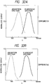
- A DMF solution obtained by dissolving 0.05 part by weight of Compound (51)(NB-404 manufactured by Nihon Kanko Shikiso) and 0.05 part by weight of Compound (56)(
Pyridine 1 manufactured by E.K) in 100 parts by weight of polyacrylnitryl (3914 manufactured by Polyscience) was applied to coating-applied paper to have a dry thickness of 10 µm. As a result, a non-visualized information recording medium was manufactured (the absorbance spectrum and the fluorescent spectrum of a sample made by applying the medium on a glass plate are shown in Figs. 32A and 32B). - The foregoing medium was irradiated with halogen light emitted from a halogen lamp (150W manufactured by Ushio Denki) having, thereon, a filter which does not allow light longer than 690 nm or longer to pass through. Then, a PIN photo-diode (PD45PI manufactured by Sharp) having a filter, which does not allow to light longer than 700 nm or shorter to pass through, was used to perform detection. A satisfactory S/N ratio of 10 or higher was realized.
- A recording medium was manufactured similar to the foregoing embodiment except for a DMF solution obtained by dissolving compound (59) in polyacryl nitril. Under the similar conditions, the measurement was performed, resulting in an S/N ratio of 2 or lower.
- A DMF solution obtained by dissolving 0.05 part by weight of Compound (51) and 0.05 part by weight of Compound (49)(NK-2782 manufactured by Nihon Kanko Shikiso and having the maximum absorbance wave length 610 nm) in 100 parts by weight of polyacrylnitril (3914 manufactured by Polyscience) was applied to coating-applied paper to have a dry thickness of 10 µm so that recording medium was manufactured. Under the similar conditions, the measurement was performed, resulting in an S/N ratio of 3 or lower.
- In second to fourth embodiments, an apparatus for detecting the non-visualized recording medium according to the first embodiment will be described.
- Although a copying machine will now be described as an applicable example of the present invention, the present invention is not limited to this. It should be understand that the present invention may, of course, be applied to a variety of apparatuses such as an image scanner connected to a computer.
- Fig. 2 illustrates the shape of the apparatus according to a second embodiment of the present invention.
- Referring to Fig. 2,
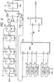
reference numeral 201 represents an image sensor portion which reads the image of an original document, converts the image into digital signals and subjects the obtained signals into a digital signal process.Reference numeral 202 represents a printer portion which forms, on a paper sheet, a full color image corresponding to the original document read by theimage scanner 201. - In the
image scanner portion 201,reference numeral 200 represents a thick plate having a mirror surface. Anoriginal document 204 placed on an original-document retaining frame glass (hereinafter called a "platen") 203 is irradiated with light emitted from ahalogen lamp 205 and passed through an infrared-ray cutting filter 208 for removing infrared rays. Reference numeral 227 represents a reflector for effectively irradiating theoriginal document 204 with light emitted from thehalogen lamp 205. Light reflected from the original document is introduced into themirrors lens 209. Therespective line sensors 210 generate full color red (R), green (G), blue (B) information components based on visible light and an infrared-ray (IR) information component based on light having the wave length outside the visible region to transmit the components to thesignal processing portion 211. Theelements element 207 is also mechanically moved atspeed 1/2v in the same direction. As a result, the entire surface of theoriginal document 204 on theplaten 203 is scanned. -
Reference numeral 5102 represents a standard white plate for use to generate correction data (shading data) for correcting scatters (scatters of the photoelectrical conversion characteristics for respective devices of the line sensors) of data items read by red, green and blue line sensors 210-2 to 210-4 for respective pixels. The standardwhite plate 5102 is substantially in while with respect to visible light as shown in Fig. 31 (the characteristics of designated by a curve 20701).Reference numeral 5103 represents a fluorescent standard plate for use to correct scatter of data read by the IR line sensor 210-1. The fluorescentstandard plate 5103 is equally applied with a fluorescent ink which generates fluorescent light having characteristics designated by a curve 20703 (see Fig. 31) when irradiated with exciting light having characteristics designated by a curve 20702 (see Fig. 31) which are substantially the same as fluorescent information to be detected as shown in Fig. 23. - In the
signal processing portion 211, signals read by the sensors 210-1 to 210-4 are electrically processed to be decomposed to magenta (M), cyan (C), yellow (Y) and black (Bk) signals which are to be transmitted to aprinter portion 202. One original-document scan (scan) performed by theimage scanner portion 201 causes one of the M, C, Y and Bk components to theprinter 202. Four times of scans of the original document is required to make one print (frame sequential image formation). - Plane-sequential M, C, Y and Bk image signals transmitted from the
image scanner portion 201 are transmitted to alaser driver 212. Thelaser driver 212 modulates and operates asemiconductor laser 213 in response to the image signals in the respective colors. Laser light beams scan the surface of aphotosensitive drum 217 by way ofpolygonal mirror 214, a f-ϑ lens 215 and amirror 216. -
Reference numeral 218 represents a rotative development unit comprising amagenta development unit 219, acyan development unit 220, ayellow development unit 221 and ablack development unit 222. The four development units alternately are brought into contact with thephotosensitive drum 217 so that M, C, Y and Bk electrostatic latent images formed on the photo-sensitive drum 217 are developed by corresponding toner. -
Reference numeral 223 represents a transfer drum around which the paper sheet supplied from apaper sheet cassette photosensitive drum 217 on to the paper sheet. - The M, C, Y and Bk colors are sequentially transferred as described above, and then the paper sheet passes through a fixing
unit 226 before it is discharged. - Fig. 13 shows the spectrum characteristics of an infrared-
ray cutting filter 208 disposed between thehalogen lamp 205 for irradiating the original document and theplaten glass 203. The infrared-ray cutting filter 208 cuts infrared rays having a spectrum characteristic of about 700 nm or longer among the infrared rays emitted from thehalogen lamp 205 shown in Fig. 14. - The
halogen lamp 205 is commonly used to read both visible information and infrared ray fluorescent information except for the visible information, thehalogen lamp 205 being arranged to emit light having both irradiation wave length components. Also the reflector 227 is commonly used to read information items of the foregoing two types. By making the irradiation system to be used commonly, the necessity of using a plurality of independent irradiation system for reading respective information items. Therefore, irradiation light beams for use to read respective information items and having different wave length components can effectively be applied to the original document. As a result, the structure of the irradiation system of the apparatus can be simplified. - Figs. 15A and 15B illustrate the structure of a
CCD 210 for use in this embodiment. - Referring to Fig. 15A, reference numeral 210-1 represents the light-receiving device array (a CCD line sensor) for reading infrared ray (IR). Reference numerals 210-2, 210-3 and 210-4 respectively represent light-receiving device arrays (CCD line sensors) for reading R, G, B wave length components.
- The four light receiving device arrays having the different optical characteristics are disposed in a monolithic manner on a silicon chip so that the IR, R, G and B line sensors are able to read the same line of the original document.
- By using the CCD line sensors structured as described above, the optical systems, such as the lens, for forming the image of the original document on to the line sensor can be made commonly with respect to reading of visible light and reading of infrared rays. Therefore, the structure can be simplified.
- Further, the accuracy in the optical adjustment for aligning the imaging position can be improved and its adjustment can also easily be performed. The structure of the CCD line sensor enables the deviation of the reading position with respect to visible light and light except for the visible light can be prevented.
- Fig. 15B is an enlarged view which illustrates the light receiving device array. Each sensor has a length of 10 µm per pixel in the main scanning direction. Each sensor has 5000 pixels in the main scanning direction (the line direction of the CCD 210) as to be capable of reading the shorter-side direction (297 mm) of an A3 original document at a resolving power of 400 dpi (dot per inch).
- The line distance of each of the R, G and B sensors is 80 µm and respectively disposed away from each other by 8 lines in the sub-scanning direction (the direction in which the optical system is moved) at 400 lpi (line per inch).
- The interval between the line of the IR sensors 210-1 and the R sensor 210-2 is determined to be 160 µm (16 lines) which is the twice of the other line intervals. By lengthening the interval between the line sensor for visible light and the line sensor for light except for the visible light as a described above, an effect can be obtained in that a filter can easily be fastened in a case where the line sensors are disposed on a silicon chip in the monolithic manner. Further, a problem to be experienced with the charge transfer portion due to the structure can be overcome as described later.
- By continuously disposing the sensors 210-2 to 210-4 for reading visible light, the IR cut filter can easily be fastened.
- The R, G and B sensors 210-2 to 210-4 have an aperture the size of which is 10 µm formed in the sub-scanning direction, while the IR sensor 210-1 has an aperture, the size of which is 20 µm which is twice the sub-scanning directional aperture. The reason for this is that the IR sensor 210-1 is enabled to read infrared fluorescent light. That is, the intensity of the fluorescent light is usually obtainable to a level about the half of that of exciting light. What is worse, the level sometimes is about 10% or less. Accordingly, this embodiment is arranged so that the light receiving area per pixel (per device) is enlarged in place of the improvement of the resolving power of the IR sensor 210-1 in the sub-scanning direction. As a result, a satisfactory dynamic range for an infrared reading signal is maintained.
- Although this arrangement is made in such a manner that the signal dynamic range is maintained by lengthening the pixel length of the IR sensor 210-1 in the sub-scanning direction, the main scanning directional length of the pixel may be lengthened by falling the resolving power in the main scanning direction in place of the sub-scanning direction.
- Each of the line sensors IR, R, G and B has an optical sensor on the surface thereof for the purpose of obtaining predetermined spectrum characteristics.
- Referring to Figs. 19 and 20, the spectrum characteristics of the R, G and B line sensors of the
CCD 210 will now be described. - Fig. 19 shows the characteristics of the filters fastened to the conventional R, G and B line sensors. As can be seen from Fig. 19, each of the conventional R, G and B filters has sensitivity with respect of infrared rays of 700 nm or longer. The infrared-ray cutting filter having characteristics shown in Fig. 20 has been fastened to the
lens 209. Since this embodiment must read the infrared component of light passed through thelens 209 by the IR sensor 210-1, thelens 209 cannot have the function of the infrared-ray cutting filter. - In order to eliminate the influence of infrared rays, the filters fastened to the R, G and B sensors are arranged to have the characteristics of each color shown in Fig. 19 and the characteristics for cutting infrared rays shown in Fig. 20.
- Fig. 16 shows the characteristics of the visible-ray cutting filter fastened to the IR sensor 210-1.
- The filter is fastened to eliminate the visible light component made incident upon the IR sensor which reads the infrared fluorescent component.
- Fig. 17 illustrates the structure of a photo-diode of the CCD. The photo-diode has an npn structure such that the upper np junction is inversely biased so that the photo-diode is formed. A
carrier 251 generated in the upper portion of a player is absorbed in the upper np junction portion as to be taken out as a signal. - Light, such as the infrared rays, inevitably generates a
carrier 252 in a deep portion of the player and acarrier 253 in a sub-straight n-layer. The carriers generated in the deep portions is, as illustrated, absorbed in the pn junction portion. Therefore, the carriers are not read as the signals. -
Characteristics 261 designated by a continuous line shown in Fig. 18 are the spectrum characteristics of a usual CCD for visible rays. As designated, the sensitivity deteriorates by about 20% with respect to infrared rays of 800 nm while having its peak at 550 nm. The thickness of the p-layer of each of the R, G and B sensors having thecharacteristics 261 is about 1000 nm. - This embodiment has an arrangement to obtain sensitivity with respect to infrared rays by making the thickness of the p-layer of the sensor 210-1 of the CCD to be thicker than that of the R, G and B sensors 210-2 to 210-4 of the CCD. That is, the thickness of the p-layer of the IR sensor 210-1 is made to be about 1500 nm so that the sensitivity peak is present at the infrared rays having the wave length ranging from 700 nm to 800 nm. The spectrum characteristics of the IR sensor according to this embodiment is designated by a
curve 262 shown in Fig. 18. - The reason why the interval between the IR sensor 210-1 and the R sensor 210-2 is to be the twice the sensor intervals between the other sensors is that the photo-diode and serial charge transfer portions formed on the both sides of the photo-diode must assuredly be separated from each other in terms of the structure. Further, the IR sensor 210-1 having a different structure, such as the different thickness of the light receiving layer, is disposed on the outside of the other sensors 210-2 to 210-4 so that the structure of the CCD is simplified.
- By widening the line intervals, the interval between the charge transfer portion for the IR signal and that for the R signal is made to be wider than the interval between the charge transfer portion for the R signal and that for the G signal and the interval between the charge transfer portion for the G signal and that for the B signal. As a result, an influence of cross talk caused by the R signal of a relatively high signal level upon the infrared fluorescent read signal, which is a small signal can be eliminated significantly.
- Since the IR sensor is disposed on the outside of the 4-line sensor, the cross talk caused from another signal can be eliminated satisfactorily.
- In this embodiment, an example of the copy-inhibited original document is an original document, on which a mark similar to a red seal is printed on the original document as shown in Fig. 1 at a predetermined position with an ink having the fluorescent characteristics with respect to infrared rays. If the foregoing mark has been detected in the infrared signal read from the original document placed on the original document retaining frame, the usual image forming operation is inhibited. The image formation is inhibited by changing image data or by turning off the power source of the apparatus as described later.
- The copy-inhibited original document is not limited to the foregoing size and the form shown in Fig. 1.
- Fig. 24 shows the reflected spectrum characteristics of the copy-inhibited original document identification mark (hereinafter called an "identification mark") included in the copy-inhibited original document according to this embodiment.
- A
curve 12201 designates the spectrum characteristics obtained by synthesizing those of thehalogen lamp 205 and the infrared-ray cutting filter 208 disposed between thehalogen lamp 205 and theplaten glass 203. In this embodiment, aninfrared ray component 12202 in the vicinity of about 700 nm among the spectrum characteristics is made to be the exciting light. Further,infrared fluorescent light 12203 having the peak at about 800 nm from the identification mark is detected so that the copy-inhibition original document is identified. In this embodiment, a halogen lamp is used as the original-document irradiation lamp for emitting both visible light component and the exciting light component with respect to the infrared fluorescent light. By fastening thefilter 208 to the halogen lamp, the wave length component (designated by thecurve 12203 shown in Fig. 24) of the infrared fluorescent light is made not to reach from the halogen lamp to the surface of the original document. - In this embodiment, the identification mark is formed by using a material which is excited by the infrared rays (the characteristics of which are designated by the
curve 12202 shown in Fig. 24) and which generates fluorescent light with respect to the infrared rays. Therefore, the characteristics of the identification mark with respect to visible light can arbitrarily be determined. Since the infrared fluorescent ink having a substantially transparent characteristic with respect to visible light is used in this embodiment, a judgment that the subject original document is the specific document, copying of which is inhibited, can be made by detecting the infrared fluorescent light in such a manner that the presence of the identification mark in the copy-inhibited original document is not made conscious for usual user of the apparatus. - The principle of reading the IR fluorescent light will now be described briefly. The
original document 204 placed on the originaldocument retaining frame 203 is irradiated with light emitted from thehalogen lamp 205 and passed through the infraredray cutting filter 208. The intensity of fluorescent light having a wave length of, for example, 800 nm and emitted from the identification mark is weak light, the level of which is lower than the half of the level of the exciting light, for example, about 10% of the exciting light. Therefore, the long wave length component containing the infrared fluorescent light wave length component of light directly reflected by the original document is cut by the infraredray cutting filter 208 so that the 800 nm wave length component made incident upon theCCD 210 is made to be substantially the fluorescent light component. As described above, the fluorescent spectrum component emitted from the identification mark of light emitted from the light source to irradiated the original document is cut. Further, the fluorescent exciting light having the wave length of 700 nm is sufficiently applied to the original document so that the S/N ratio of the fluoresent signal emitted from the identification mark can be improved. - Light reflected from the original document passes through the
mirrors CCD 210, the line sensors being sensors for reading the full color red (R) information component, the green (G) information component, the blue (B) information component and the infrared (IR) information component. - Since the R, G and B line sensors 210-2 to 210-4 have the R, G and B filters having the characteristics with which the 700 nm exciting light can sufficiently be decayed and which are shown in Fig. 20, full-color reading can be performed while eliminating the influence of the 700 nm infrared fluorescent exciting wave length light and the infrared fluorescent light.
- Since the IR sensor 210-1 has the filter for cutting light having the wave lengths shorter than 700 nm as shown in Fig. 16, only the
infrared fluorescent component 12203 shown in Fig. 24 is read. The foregoing filters enable infrared fluorescent light to be extracted simultaneously with the operations of reading the original document and recording the image. Therefore, an excessive operation of scanning the original document, such as a pre-scanning detection of only the identification mark with the infrared fluorescent light can be omitted. If a user does not place the copy-inhibited original document at the time of the pre-scanning operation but places the copy-inhibited original document at the time of the main scanning operation, copying can effectively be inhibited. - As a result of the foregoing structure, the visible color region and the infrared region of the identification mark can satisfactorily be separated from each other at the time of simultaneously reading the two regions while necessitating only one scanning operation.
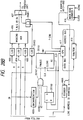
- Figs. 4A and 4B are block diagrams which illustrates the structure of the
signal processing portion 211 of theimage scanner portion 201 and the flow of the image signal realized in the foregoing structure. The image signal transmitted from theCCD 210 is received by an analogsignal processing portion 4001. In the analogsignal processing portion 4001, the signal is converted into an 8-bit digital image signal. Then, the 8-bit digital image signal is received by ashading correction portion 4002.Reference numeral 4008 represents a decoder which decodes a main scanning address obtained from a mainscanning address counter 419 to generate a line-unit CCD drive signal, such as a shift pulse and a reset pulse. - Fig. 21 is a block diagram which illustrates the analog
signal processing portion 4001. Since the circuits for processing the IR, R, G and B signals are in the same form, one of the circuits will now be described. The image signal transmitted from theCCD 210 is sampled and held in a sampling and holding portion (an S/H portion) 4101 to stabilize the wave form of the analog signal. ACPU 417 controls avariable amplifier 4103 and aclamping circuit 4102 via avoltage control circuit 4103 to cause the image signal to use fully the dynamic range of an A/D converter 4105. The A/D converter 4105 converts the analog image signal into an 8-bit digital image signal. - The 8-bit digital image signal is, in the
shading correction portion 4002, subjected to a shading correction process by a shading correction method. - The
CPU 417 receives the reading signal obtained from the IR sensor 210-1 causes the read infrared fluorescent signal for one line supplied from the fluorescentstandard plate 5103 to be stored in aline memory 4003. Further, a multiplexing coefficient for making read data for each pixel recorded on theline memory 4003 to be level 255 is obtained for each pixel to store it in acoefficient memory 4006 for one line. In synchronization with an output of each pixel due to reading of the line of the IR sensor 210-1 at the time of reading the original document, the multiplexing coefficient corresponding to the pixel is read from the coefficient memory. Amultiplier 4007 multiplies each pixel signal obtained from the IR sensor 210-1 by the multiplexing coefficient so that the shading correction of the infrared fluorescent light is performed. - Also the shading corrections of the R, G and B signals are, similarly to that of the IR signal, performed in such a manner that the reading signal for one line obtained from the standard
white plate 5102 is written on the line memory. Further, the multiplexing coefficient for making the value to be 255 is stored in the coefficient memory. Then, the multiplier multipliers the read signal by the multiplexing coefficient for each pixel obtained from the coefficient memory. - Since the light receiving portions 210-1, 210-2, 210-3 and 210-4 of the
CCD 210 are disposed away from each other as shown in Figs. 15A and 15B, the spatial deviation in the sub-scanning direction is corrected byline delay devices Reference numerals Reference numeral 406 represents a known masking and UCR circuit which receives three primary color signals to transmit Y, M, C and Bk signals while having a predetermined bit length, for example, 8 bits whenever the respective reading operations are performed. - Fig. 23 is a block diagram which illustrates a light-quantity control portion for controlling the
halogen lamp 205.Reference numeral 4301 represents the light quantity control portion for controlling thehalogen lamp 205. - A method of adjusting the light quantity of the
halogen lamp 205 and a method of controlling thevariable amplifier 4103 and theclamping circuit 4102 will now be described with reference to a flow chart shown in Figs. 22A and 22B. - In the analog
signal processing portion 4001, the amplification rate of thevariable amplifier 4103 is adjusted in accordance with image data obtained by reading the standardwhite plate 5102 in the case of the R, G and B signals in order to fully use the dynamic range of the A/D converter 4105. In accordance with image data obtained in a state where theCCD 210 is not irradiated with light, the control voltage of theclamping circuit 4102 is adjusted by avoltage control circuit 4103. In the case of the IR signal, the image data obtained at the time of reading infrared fluorescent information from the standardwhite plate 5102 is used to perform the adjustment similarly to the R, G and B signals. - When an adjustment mode is commenced by a control portion (omitted from illustration), the reflecting
mirror 206 is moved to a position below the standardwhite plate 5102 to set a predetermined gain into thevariable amplifier 4103 for adjusting the halogen lamp (step 1). Image data obtained in the state where theCCD 210 is not irradiated with light is caused to be received into the line memory (a shading RAM) 4003. The received data is calculated by theCPU 417 to control thevoltage control circuit 4103 in such a manner that the mean value of image data for one line is made nearest 08H, and the reference voltage of theclamping circuit 4102 is adjusted (steps 2 and 3). Then, the control value after the adjustment has been performed is stored in aRAM 418 attached to the CPU 417 (step 4). - Then, image data obtained by reading the standard
white plate 5102 by turning on thehalogen lamp 205 is received by theline memory 4003. Further, the peak value of the G signal is made to be a value between D0H and F0H by the lightquantity control portion 4301 controlled by the CPU 417 (halogen lamp adjustment operation in steps 5 and 6). The adjusted control value is caused to be stored in theRAM 418 attached to the CPU 417 (step 7). Then, image data obtained by reading the standardwhite plate 5102 by lighting on thehalogen lamp 205 to emit a light quantity adjusted insteps 5 and 6 is caused to be received by theline memory 4003 corresponding to red, green and blue. The peak value of the image data is made to be a value between E0H and F8H for each of red, green and blue by controlling thevoltage control circuit 4103, and the amplification ratio of thevariable amplifier 4103 is adjusted for each of red, green and blue (steps 8 and 9). Further, the adjusted amplification ratio is, as the gain gate (hereinafter called "H-gain data") at the time of using thehalogen lamp 205, stored in theRAM 418 attached to theCPU 417. - Then, operations for adjusting the clamping circuit and the variable amplifier of the analog signal processing portion for processing the read signals supplied from the IR sensor 210-1 and an operation for storing the control value will now be described. The fluorescent
standard plate 5103 is read by turning of thehalogen lamp 205 and by moving the reflectingmirror 206 to a position below the fluorescent standard plate 5103 (step 11). Image data obtained in the state where theCCD 210 is not irradiated with light is received by the line memory for the IR signal. The received image data is calculated by theCPU 417. The mean value of image data for one line is made nearest 08H by controlling thevoltage control circuit 4103 to control adjust the reference voltage of the clamping circuit 4102 (steps 12 and 13). The adjusted control value is stored in theRAM 418 attached to the CPU 417 (step 14). Then, infrared fluorescent image data obtained by reading the fluorescentstandard plate 5103 by lighting on thehalogen lamp 205 to emit the light quantity adjusted insteps 5 and 6 is received by the line memory for the IR signal. The peak value in one line of image data of the IR signal is made to be a value in a range from E0H to F8H by controlling thevoltage control circuit 4103 for the IR signal to adjust the amplification rate of thevariable amplifier 4103 for each of red, green and black (steps 15 and 16). The amplification rate is, as the gain data for the IR signal, stored in theRAM 418 attached to theCPU 417 so that the halogen lamp is lit off (step 17). - The control data obtained in the foregoing adjustment mode is set to each control portion at the time of supplying the electric power.
- The usual copying operation and an operation for judging the fluorescent mark will now be described.
- When an operator places an original document on the
platen 203 and the copying operation is commenced by using a control portion (omitted from illustration), theCPU 417 controls a motor (omitted from illustration) to move the reflectingmirror 206 to a position below the standardwhite plate 5102. - Then, the halogen lamp is lit on to irradiate the standard
white plate 5102 with light. Further, theshading correction portion 4002 performs shading corrections for the R, G and B signals. - Then, the CPU lights on the halogen lamp 5101 to irradiate the fluorescent
standard plate 5103. Theshading correction portion 4002 performs a shading correction for the IR signal by using infrared fluorescent light. - Then, the original reading operations are performed four times in accordance with the image recording operations for M, C, Y and Bk in the printer portion so that a frame-sequential image recording operation is performed. Further, the fluorescent mark is detected simultaneously with each reading operation. In accordance with the result of the detection, the recording operation is controlled.
- In this embodiment, the four times of the reading operations (scans) is needed to copy the original document. The operations of the
image scanner 201 and theprinter 202 at each scan are shown in Fig. 3. - That is, if the counterfeit prevention of a copy-inhibited original document is performed, the image scanner coarsely detects the position of the fluorescent mark in
Mode 1 and the printer portion transmits a magenta image at the first scan. - At the second scan, the image scanner is in
Mode 2 in which the fluorescent mark is extracted from the position of the fluorescent mark detected at the first scan to store the data in the memory to judge whether it is a predetermined copy-inhibited mark. The printer portion transmits a cyan image. - At the third and fourth scans, the image scanner is in
Mode 3 so that a specific process for preventing the counterfeit is performed if a judgment has been made in the second scan that the counterfeit is intended. For example, any one of the following operations is performed: a yellow or black solid printing (to be described later) is performed; yellow and black images are not formed; and the power of the fixing unit is turned off. - Fig. 5 illustrates the operation timing of each portion of the image scanner portion according to this embodiment.
- VSYNC signal is an image effective region signal in the sub-scanning direction. In a region where the VSYNC signal is "1", sequential (M), (C), (Y) and (Bk) output signals for reading (scanning) the image are formed. Signal VE is an image effective region signal in the main scanning direction. In a region where the signal VE is "1", timing of the main scanning commencement position is arranged. Signal CLK is a pixel synchronizing signal. At the first transition timing from "0" to "1", image data is transferred. Signal CLK8 is a timing signal at intervals of 8 pixels. At the first transition timing from "0" to "1", timing of a signal subjected to an 8 x 8 block process is arranged.
- The fluorescent mark detection performed by the internal block of the
image scanner 201 shown in Figs. 4A and 4B and a portion for generating an image to be recorded by the printer will now be described.Reference numerals Reference numeral 406 represents a known masking and UCR circuit which receives three primary color signals to transmit Y, M, C and Bk signals while each having a predetermined bit length of, for example, 8 bits, whenever the reading operations are performed.Reference numeral 407 represents an OR gate circuit which calculates a logical OR with a value stored in aregister 408. Theregister 408 usuallly stores 00H written thereon so that an output from the masking andUCR circuit 406 is transmitted to the printer portion as it is. At the time of performing the counterfeit prevention, theCPU 417 sets FFH into theregister 408 via a data bus so that a solid yellow or black toner image is transmitted. -
Reference numeral 417 represents a CPU for controlling the apparatus in each mode.Reference numeral 4009 represents a binary coding circuit which binary-codes the infrared fluorescent signal at an adequate slice level. Among the outputs from the binary coding circuit, output "1" means the presence of the fluorescent mark and output "0" represents that no fluorescent mark is present, the outputs being transmitted for each pixel. - In a
block processing circuit 409, an 8 x 8 block process is performed so that the output from thebinary coding circuit 409 is processed for each 8 x 8 block. -
Reference numeral 412 represents a read and write enabled random access memory (RAM). Data is changed over by aselector 411 and the address is changed over by aselector 413. -
Reference numeral 419 represents a main scanning counter which is reset in response to HSYNC signal and the count of which is increased at the timing of CLK signal to generate 13-bit main scanning addresses (hereinafter called "X address") X12 to X0. -
Reference numeral 420 represents a sub-scanning address counter which is reset when the VSYNC signal is in the region "0" and the count of which is increased at the timing of the HSYNC signal to generate 13-bit sub-scanning addresses (Y address) Y12 to Y0. - The
CPU 417 controls theselectors address decoder 414 in accordance with each mode to read/write data to and from theRAM 412.Reference numeral 418 represents a RAM/ROM attached to theCPU 417.Reference numeral 410 represents a fluorescent mark detection circuit for detecting the position of the fluorescent mark. - Fig. 6 illustrates the detailed internal structure of the
block processing circuit 409 shown in Figs. 4A and 4B. -
Reference numerals 701 to 708 represents seven D-flip flops (hereinafer called "DEFs") disposed in series which sequentially delay the input signals in response to the pixel clock signal CLK, theDEFs 701 to 708 being cleared when VE = "0", that is, in a non-image region. -
Reference numeral 738 represents a 4-bit up/down counter, 737 represents an EX-OR gate, and 740 represents an AND gate which is operated as follows.Table 1 VSYNC VE Xt Xt-8 Output from counter 0 X X X 0 (clear) X 0 X X 0 (clear) 1 1 0 0 held 1 1 0 1 count down 1 1 1 0 count up 1 1 1 1 held - That is, the output from the
counter 738 is cleared to zero in a region where VSYNC or VE is "0", the same is held when Xt = Xt-8, its count is increased when Xt = 1 and Xt-8 = 0, and its count is decreased when Xt = 0 and Xt-8 = 1. By latching the output from thecounter 738 by alatch 739 withCLK 8 the period of which is 8 clocks, the sum (number of cases where Xt = 1) of eight input data items Xt is transmitted. - Data items for eight lines of the foregoing outputs are simultaneously supplied to an
adder 741 byFIFO memories 721 to 727 for one line to transmit the sum. As a result, total SUM, which is the sum of the cases where number of 1 in the 8 x 8 window) are transmitted in the form of 0 to 64. -
Reference numeral 742 represents a digital comparator which subjects the output SUM from theadder 741 and a predetermined comparative value TW determined by theCPU 417 to a comparison. The result of the comparison is transmitted while being formed into "0" or "1". - By previously setting an adequate number to TW, noise elimination can be performed in 8 x 8 block units.
- Figs. 7A and 7B illustrate the fluorescent
mark detection circuit 410. -
Reference numeral 827 represents a line thinning circuit which transmits the VE signals for 8 lines while thinning to one line. Since writing of data on each FIFO memory is controlled by using the VE signals thinned to 1/8, the contents of each FIFO memory is updated at every 8 lines. Since each F/F is operated in response to the CLK8, the operation of the foregoing circuit is performed in units of 8 pixels/8 lines. -
Reference numerals -
Reference numerals 831 to 841 represent DEFs disposed in units of three DEFs in series to correspond to the output for the four lines. All DEFs are operated in response to theCLK 8. If one or more 1 (the fluorescent mark) are present in the 4 x 4 region, the 4 x 4 region (a 2 mm x 2 mm region on the original document) is fully made to be 1 by theOR gate 857. As a result, the gap of the mark is covered as the fluorescent mark portion. -
Reference numerals -
Reference numerals 845 to 856 represent DEFs disposed in units of three DEFs in series to correspond to the output for the four lines. All DEFs are operated in response to the CLK8. The ANDgate 858 transmits 1 denoting the 4 x 4 region is fully 1 (the fluorescent mark is present). As a result, the portion expanded as the fluorescent mark portion on the outside of the mark at the time of covering the gap of the mark is restored to have the original size. Therefore, the undesirable expansion of the noise component of the fluorescent signal occurring due to contamination of the original document or the like can be prevented. -
Reference numerals 819 to 821 represent 18 FIFOs each of which realizes a delay of one line so that 19 lines are processed simultaneously. -
Reference numerals 801 to 816 represent DEFs disposed in units of 10 DEFs in series to correspond to the outputs for 19 lines.Reference numerals DEF 812. All DEFs are operated in response to the CLK8. When all outputs from theDEFs DEFs gates 823 to 825. - One block is arranged to be 8 pixels/8 lines which correspond to about 0.5 mm x 0.5 mm on the original document. That is, when the fluorescent marks are continued for 9.5 mm in both longitudinal and the lateral directions, the substantially the central position of the mark at this time is, as Position Data, latched by the
latch 826 and transmitted to the CPU. By determining the size of 9.5 mm to be somewhat smaller than the size of the mark in the copy-inhibited original document, the position of the mark can assuredly be detected while eliminating the influence of the noise component. - Fig. 8 is a block diagram which illustrates the
address decoder 414. -
Reference numerals registers -
Reference numerals Reference numeral -
Reference numerals 918 to 920 represent AND gates. If a resulted value BXY is written on theregister 909, the case where the following relationships are held:
Allow to the following outputs to be transmitted:
Xou = X address - RX1
You = Y address - RY1
Enab = 1. - That is, the area of the size BXY is subjected to addressing while making RX1 and RY1 to be leading addresses with respect to the main scan and the sub-scan.
- Fig. 3 shows the relationship among the four times of scans from the first scan to the fourth scan, the three modes of the image scanner from
Mode 1 toMode 3 and the contents of the outputs from the printer portion. - Fig. 9 shows the flow of a process of control performed by the CPU. As shown in Fig. 9,
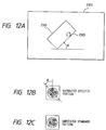
MODE 1 for the first scan is set to the CPU instep 1001. - In the foregoing state, the first scan is commenced in
step 1002. InMode 1, the magenta output is transmitted from the printer and the coarse central position of the fluorescent mark portion in the copy-inhibited original document is detected. - Fig. 1 illustrates a state where a copy-inhibited original document corresponding to a tenthousands-yen bill is placed on the original document retaining frame. At the first scan, that is, in
Mode 1, the address of the central portion of the fluorescent mark portion designated by diagonal lines, that is, a portion corresponding to (Xc, Yc) which is a portion corresponding to (Xc, Yc) shown in Fig. 1 is latched by thelatch 826 and transmitted to the CPU. - The CPU is able to coarsely detect the value of (Xc, Yc) which is the center of the fluorescent mark.
- In
next step 1006,Mode 2 for the second scan is set. That is, theselector 411 is set to B, theselector 413 is set to A and theselectors - In the
address decoder 414, setting is performed in such a manner that the position of the fluorescent mark is made to be as follows:
RX1 = XS1 RY = YS1 (in one pixel unit). where Xc and Yc are data items about the central position of the mark in the detection range of 9.5 mm as described in the description of the mark detection circuit shown in Figs. 7A and 7B. In order to completely cover the fluorescent mark range, the diameter of which is 10 mm to 20 mm, pixels are set to BXY by a number (472 at 400 dpi) corresponding to about 30 mm. - As the leading address XS1 and XY1, values more adjacent by 15 mm (236 pixels at 400 dpi) to the origin than Xc and Yc are set.
- In
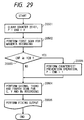
step 1007, the second scan is performed so that a binary-coded fluorescent signal obtained from a dashed line region including the fluorescent mark shown in Fig. 1 is written on theRAM 412. - Further, a judgement whether or not the fluorescent mark is present is made in
step 1008 in accordance with an algorithm to be described later. If a judgement is made instep 1009 that there is no possibility of the counterfeit, that is, if no fluorescent mark has been detected, the flow proceeds to step 1010 in which the third and fourth scans are performed and a usual operation is performed so that development is performed by using Y, M, C and Bk toner. Instep 1012, the developed image is fixed and the fixed image is transmitted. - If a judgement has been made in
step 1009 that there is a possibility of the counterfeit, that is, if the fluorescent mark has been detected, a counterfeit prevention is performed instep 1011. Specifically, the CPU sets FFH (usually OOH is set) to theregister 408 shown in Figs. 4A and 4B so that FFH is transmitted to the printer portion. As a result, Y and Bk toner is allowed to adhere to the entire surface, causing the usual copying operation to be inhibited. - Pattern matching of the fluorescent mark in
step 1008 will now be described. Since there is a possibility that different marks are formed between the two sides of a bill or the like at the time of forming the fluorescent marks, two fluorescent mark patterns are previously registered for pattern matching in order to one kind of the copy-inhibited original document. - When a specific portion of a specific document is written on the
RAM 412, theCPU 417 refers the contents of theRAM 412 so that pattern collating is performed. A flow chart of pattern collating is shown in Fig. 10. TheRAM 412 has binary-coded data of the specific portion stored therein. - The foregoing area is subjected to a process in
step 2102 and ensuing steps. Instep 2102, a window process is performed for eliminating noise. - Assumptions are made that the binary-coded image in the
area 1 is 2201 shown in Fig. 11 and that a small square shows one pixel, a full while portion shows a white pixel and a diagonal line portion shows a black pixel. The foregoing portion is scanned with awindow 2202 the size of which is 2 x 2 pixels to count the number of the black pixels in the window. A portion in which the result of counting is larger than 2 is made to be a novel black pixel. Therefore, the result of the process is contracted to the half in both longitudinal direction and the lateral direction as designated byreference numeral 2203. As a result, a pattern, from which noise has been eliminated, can be obtained. Since the number of the black pixels in the window at aposition 2202 is 1, the portion is, as a white pixel, replaced by aposition 2204. - Then, the center of
gravity 1 of thepattern 2203 is calculated. - The center of
gravity 1 can be calculated by a known method by projecting thepattern 2203 in both longitudinal direction and the lateral direction. - Then, the similarity is calculated by standard pattern matching. First, a standard pattern previously registered as a dictionary is read from the
ROM 418 shown in Figs. 4A and 4B to the CPU instep 2105. The standard pattern is the fluorescent pattern of the subject copy-inhibited original document. Since the pattern extracted untilstep 2103 is completed has a possibility that the original document has been rotated due to the angle of the placement of the original document, a satisfactory effect cannot be obtained if the foregoing pattern is subjected to a comparison with a single standard pattern. - The foregoing state is shown in Figs. 12A to 12C. The standard pattern may be set in such a manner that a plurality of patterns consisting of the fluorescent patterns rotated at angular intervals of several degrees are previously stored in the ROM as to be selected to be read to the CPU. As the plural patterns, 24 patterns consisting of marks rotated at angular intervals of 15 degrees from zero degree to 360 degrees are used. Therefore, a variety of methods for calculating the similarly may be employed as exemplified by the following method: as shown in Figs. 12A to 12C, the pattern extracted to the foregoing moment is made to be as shown in Fig. 12A and the standard pattern having a predetermined rotational angle and selected from patterns which are rotated by the angular intervals of 15 degrees by the foregoing method is made to be as shown in Figs. 12B and 12C, the foregoing patterns being expressed by B (i, j) and P (i, j), respectively (B (i, j) is 1 in the case of the black pixel and the same is zero in the case of the white pixel). When coordinates of the center of gravity of B (i, j) obtained in
step 2104 shown in Fig. 10 is (iBC, jBC) and the coordinates of the center of gravity of P (i, j) obtained similarly is (iPC, iPC), the similarity COR of the two patterns is expressed by the following equation:
where ⊕ is the exclusive OR of P and B, and Equation (1) shows the Hamming distance when the center of gravity of the pattern B (i, j) are aligned to each other. The similarity of the two patterns is raised in proportion to the COR. - This embodiment is arranged in such a manner that the reliability of the similarity is improved and the generation of an error in recognition is prevented by using Equation (2) formed by deforming Equation (1) so that the similarity COR is obtained.

where the AND
- When the similarity COR is calculated by the foregoing method, a comparison is made in 2107 between previously obtained Th and the COR.
- If COR > Th, a judgement is made that the fluorescent mark is present. Therefore, a discrimination is made that the copy-inhibited original document is present (2108), and the collating operation is completed.
- If COR < Th, a judgement is made that no fluorescent mark is not present in the subject area. Therefore, a discrimination is made that no copy-inhibited original document is present (2110), and the collating operation is completed.
- This embodiment is arranged in such a manner that the presence of fluorescent light is detected in place of detecting the pattern expressed by infrared fluorescent information in the copy-inhibited original document.
- Among the copy-inhibited original documents such as bills, some kinds of bills are made of paper composed of the fiber containing a substance having the fluorescent characteristics as exemplified by Canadian dollar. In this embodiment, infrared fluorescent light is detected in thin line information such as the foregoing fiber so that the copy-inhibited original document is detected.
- A control block according to this embodiment is shown in Figs. 25A and 25B. In this embodiment, the number of pixels of fluorescent information contained in the original document is counted in place of performing pattern matching of the fluorescent mark.
- Referring to Figs. 25A and 25B, the same elements as those shown in Figs. 4A and 4B are given the same reference numerals.
Reference numeral 20101 represents a counter which counts the number of fluorescent pixels in the original document with CLK. In this embodiment, an 8-bit counter is used to add the fluorescent pixels, the number of which is 255 pixels or less.Reference numeral 20202 represents a 4-input AND gate which supplies a binary-coded fluorescent signal transmitted from thebinary coding circuit 4009 as an enable signal of thecounter 20101 when the main scanning region signal VE and the sub-scanning region signal VSYNC are generated. Thecounter 20101 is cleared to zero in response to CLR signal supplied from the CPU, and the clear signal sets the flip-flop (F/F) 20103 to validate the output from thegate 20102. - In a case where a binary-coded signal is supplied by a number larger than the maximum count 255 for the
counter 20101, RC signal is generated at a moment the output from thecounter 20101 is 255 so that the F/F 20103 is reset. Therefore, the enable input of the counter is forcibly made to be "0" to maintain the output from the counter at 255. - The
CPU 417 reads the result of counting performed by thecounter 20101 as CNT signal. If the result of counting is larger than a predetermined value (for example, larger than 128 pixels), a fact is detected that the copy-inhibited original document is being copied. - Fig. 26 shows the flow of the process to be performed by the CPU according to this embodiment.
- In
step 20201, the CPU clears thecounter 20101 and the F/F 20103. - In
step 20202, the first scan is commenced. At this time, the printer transmit a magenta output, and the number of pixels in the fluorescent information obtained from the original document is counted. - In
next step 20203, a judgement is made whether or not the number of the fluorescent pixels is larger than a predetermined value (128). If a judgement is made instep 20203 that there is no possibility of counterfeit, that is, the number of the fluorescent pixels is smaller than a predetermined value, the second, third and fourth scans are performed instep 20204. As a result, a usual operation is performed in such a manner that M, C, Y and Bk toner are used to develop the image and the toner image is fixed and transmitted instep 20205. - If a judgement is made in
step 20203 that there is a possibility of counterfeit and if the fluorescent pixels by a number larger than a predetermined value are detected, a counterfeit prevention process is performed instep 20206. Specifically, FFH (usually OOH is set) is set to theregister 408 shown in Figs. 4A and 4B so that FFH is transmitted to the printer portion. Then, C, Y and Bk toner is allowed to adhere to the entire surface to inhibit the copying operation. - This embodiment is directed to detect fluorescent light in place of detecting infrared fluorescent information in the copy-inhibited original document similarly to the second embodiment.
- In this embodiment, the presence of the fluorescent mark except for the visible light, such as infrared rays, contained in the copy-inhibited original document is detected, the fluorescent information is converted into visible information, and it is recorded together with visible information obtainable from the original document. As a result, normal recording of the copy-inhibited original document is inhibited.
- As effective fluorescent information about the copy-inhibited original document according to this embodiment, it is preferable to use a substance formed by recording a regular pattern on the entire surface of the original document or a substance formed by painting fluorescent information on the entire surface of the original document as shown in Fig. 27. If the fluorescent information has transparent characteristics with respect to visible light, no practical problem usually arises in a normal way of usage except for the unlawful copying operation.
- A control block according to this embodiment is shown in Figs. 28A and 28B. In this embodiment, the number of pixels of fluorescent information contained in the original document is counted in place of performing pattern matching of the fluorescent mark similarly to that shown in Figs. 25A and 25B. Referring to Figs. 28A and 28B, the same elements as those shown in Figs. 25A and 25B are given the same reference numerals.
-
Reference numeral 20401 represents an AND gate. A signal obtained by converting the light quantity and density of the infrared fluorescent reading signal IR is validated in response to P-ENB signal supplied from theCPU 417 instep 20402. The ORgate 407 synthesizes the validated signal with a usual visible image to be recorded. The phase deviation of the IR signal occurring when it is read by the CCD from the visible information in the sub-scanning direction has been corrected by a delay means 401. If an arrangement is made that Moire fringes or the like are generated by fluorescent information and visible information when fluorescent information is printed on to the copy-inhibited original document, the intended effect of the copy inhibition by means of the Moire can be obtained satisfactorily. - The
CPU 417 reads the result of counting performed by thecounter 20101 as CNT signal. If the result of counting is larger than a predetermined value (for example, 128 pixels or more), a fact that the copy-inhibited original document is being copied is detected, casing the P-ENB signal to be made "1". As a result, infrared fluorescent information is visualized and the usual copying operation is inhibited. - Fig. 29 shows the flow of the process performed by the CPU according to this embodiment.
- In
step 20501, the CPU clears thecounter 20101 and the F/F 20103, and makes the P-ENB signal to be "0". - In
step 20502, the first scan is commenced. In this embodiment, the printer transmits a magenta output and the number of pixels of fluorescent information obtained from the original document is counted. - In
step 20503, whether or not the number of fluorescent pixels is larger than a predetermined number (128) is judged. If a judgement is made instep 20503 that there is no possibility of counterfeit, that is, the number of the fluorescent pixel is smaller than a predetermined number, the second, third and fourth scans are performed instep 20504. Then, a usual operation is performed such that M, C, Y and Bk toner images are developed and the developed image is fixed and transmitted instep 20505. - If a judgement is made in
step 20503 that the fluorescent pixels are detected by a number larger than a predetermined number and a judgement is made that there is a possibility of the counterfeit, a counterfeit prevention process is performed instep 20506. Specifically, the P-ENB signal is made to be "1" and a record image formed by synthesizing fluorescent information as visible information is transmitted to the printer portion at the time of recording C, Y and Bk images. As a result, a normal copying operation is inhibited. - The foregoing embodiment is arranged in such a manner that infrared ray component adjacent to about 700 nm is used as the exciting light and that infrared fluorescent light having the peak at about 800 nm is caused to emit from an identification mark. Another arrangement may be employed in which light in a visible light region is used as the exciting light and information denoting the copy-inhibited original document is formed by a fluorescent ink so as to cause the infrared fluorescent light of, for example, 700 to 800 nm to be emitted.
- As contrasted with the foregoing embodiment in which the filters for cutting infrared light shown in Fig. 20 are used as the R, G and B reading CCD filters, a filter for cutting the wave lengths longer than 650 nm shown in Fig. 20 is used as the
filter 208 for cutting infrared rays at the light source. - As a result, light received by the R, G and B line sensors is only infrared ray obtained from the identification mark in the copy-inhibited original document or infrared fluorescent light emitted in a special case. Therefore, a necessity for the R, G and B reading CCD to have the characteristic to cut the infrared rays containing the near infrared rays longer than 650 nm can be eliminated. As a result, the cost of the CCD can be reduced.
- Another structure may be employed in which ultraviolet region light is used as the exciting light and information denoting the copy-inhibited original document is formed by a fluorescent ink so as to cause infrared fluorescent
light having wavelengths 700 to 800 nm to be emitted. - In this case, a metal halide lamp or the like is used as the light source which emits light containing an ultraviolet component as contrasted with the first embodiment. Further, a filter for cutting light having the wave length longer than 650 nm shown in Fig. 20 is used as the
filter 208 for cutting infrared rays at the light source. Thus, direct reflected light of infrared ray from the light source cannot be made incident on the R, G, B and IR sensors. The spectrum characteristics of light with which the original document is irradiated are designed byreference numeral 20601 shown in Fig. 30. The filters for the R, G and B reading CCD comprise filters having both spectrum characteristics for R, G and B shown in Fig. 19 andcharacteristics 20604 shown in Fig. 30 with which ultraviolet light shorter than 400 ns and infrared rays longer than 650 nm can be cut. The IR sensor has a filter having characteristics for cutting both visible component and the ultraviolet component shown in Fig. 16 to read only ultraviolet fluorescent component only. By using ultravioletexciting light 20602, the wave length of which is short and which has relatively large light energy than visible light and infrared rays,infrared fluorescent light 20603 having higher level energy can be obtained. As a result, the fluorescent mark (the identification mark) can further assuredly be recognized. - The CCD shown in Figs. 15A and 15B is not limited to the CCD for reading infrared fluorescent information and visible information. It may also be used to read visible information and infrared information. In this case, a sensor having a thick light receiving layer and capable of reading infrared rays is disposed on the outside of the visible information reading sensor.
- The CCD shown in Figs. 15A and 15B is not limited to the CCD capable of reading infrared information except for visible information and visible information. It may also be used to read ultraviolet information except for visible information and visible information. That is, short wave length ultraviolet information can be effectively read only in a case where a thin photoelectric conversion layer is used which is composed of the p-layer attributing to the photoelectrical conversion and the n-layer formed on the p-layer shown in the cross sectional structural view shown in Fig. 17. Therefore, the photo-diode and charge transfer portions usually formed on the two sides of the photo-diode and performing the serial operation must be assuredly separated from each other in terms of the structure to prevent electric induction. Hence, the intervals between the ultraviolet light reading sensor and the other sensors must be widened as compared with the other sensor intervals. In addition, a sensor having a light receiving layer formed into a different structure is disposed on the outside of the other sensors to simplify the structure of the CCD.
- The CCD shown in Figs. 15A and 15B is not limited to the CCD for reading infrared fluorescent information and visible information. It may also be used to read visible information and ultraviolet information or read visible information and infrared information. That is, the fluorescent light reading sensor is disposed on the outside of the plural line sensors or the line interval is widened as compared with the line intervals between the other sensors for the purpose of reading weak fluorescent information so that cross talk from information except for the fluorescent information can be prevented. An infrared information reading sensor is disposed on the outside of the visible information reading sensor.
- In all embodiments described above, a common irradiation system for reading visible information and for exciting fluorescent light is disposed. Light may be emitted from a structure composed of irradiation lamps having different characteristics. The combination is exemplified by a combination of an FL lamp for visible light and a halogen lamp for infrared exciting light and a combination of a halogen lamp for reading visible light and an FL lamp (black lamp) for generating only ultraviolet exciting light.
- Although the foregoing embodiments are arranged in such a manner that the standard white plate is used to correct the visible light read data and to correct the infrared fluorescent data, a standard white plate for correcting the visible light and a standard plate for correcting the infrared fluorescent light may independently be used at different positions.
- As the common standard plate, a structure may be employed which is formed by stacking a standard plate, which is white with respect to visible light, and infrared fluorescent material exhibiting substantially transparent characteristics with respect to visible light.
- As described above, the foregoing embodiments according to the present invention are arranged so that fluorescent information which is substantially transparent with respect to visible light is used to detect the specific document. As a result, the copy-inhibited original document can be detected while eliminating an influence upon the actual state of usage with visible light.
- Since original document information is judged by using information except for visible information, the judgement information contained in the original document can be discriminated in the visible manner. Therefore, the discrimination cannot be made by a usual image reading means. As a result, the security protection against the copy inhibition operation of the copy-inhibited original document can further be improved. Since the specific original document is identified by using information except for visible information, information which can easily erroneously be discriminated as identification information can intentionally be reduced as compared with a case where visible information is used. Therefore, a further accurate identification of the specific document can be performed.
- Since information, which cannot be identified with visible light, is recorded as visible information, an unlawful copied product from the copy-inhibited original document can easily be discriminated.
- According to the present invention, visible information and information except for the visible information are simultaneously read, and the original document is discriminated by using information except for the visible information. Therefore, while discriminating the original document in a real time manner at the time of the image data output operation, the accuracy in discriminating the original document can be improved as compared with a case where visible information is used. As a result, the copy inhibition operation of the copy-inhibited original document can effectively be performed.
- Further, information of the copy-inhibited original document except for the visible information can be converted into visible information in a real time manner during the output of visible information and it can be transmitted together with visible information obtained from the original document. Therefore, a complete visible data output from the copy-inhibited original document can be inhibited while simplifying the control structure.
- Further, the irradiation for reading the visible information and information except for the visible information is made common, and the visible information and the information except for the visible information are separated from each other by using independent sensors. Therefore, the intensities of irradiation light for the visible information and the information except for the visible information can be strengthened while necessitating a simple structure. Further, sensors are independently used for reading the visible in formation and the information except for the visible information. Hence, the gain of each reading signal can be set to an adequate level. As a result, the S/N ratio of the visible information and the information except for the visible information can be made optimum. Consequently, the original document can precisely be read and the original document can accurately be discriminated with a simple structure.
- Since the filter is disposed in the optical passage formed from the original-document irradiation lamp to the original document to allow the exciting wave length component of the fluorescent component to pass through and to decay the fluorescent wave length component, reading of the fluorescent information can be performed while realizing an excellent S/N ratio.
- By disposing the filter in the rear of the common optical system for visible light and light except for the visible light and as well as in front of the visible light reading sensor to cut the wavelengths except for the visible wave lengths, the visible information can be read while eliminating the influence of the light except for the visible light.
- By disposing the filter in the rear of the common optical system for visible light and light except for the visible light and as well as in front of the sensor for reading light except for the visible light to cut exciting light with respect to fluorescent light or visible light, light except for visible light can be read while maintaining an excellent S/N ratio.
- Since fluorescent information generated under the irradiation of a conventional halogen lamp of the like which emits infrared light by a large quantity is used, copy-inhibited information can assuredly be detected.
- In the present invention, the sensor for detecting light information except for visible information and the sensor for reading the visible information are structured by the monolithic manner. Therefore, the necessity of maintaining an optical passage by using a special optical system such as a prism to read information except for the visible information can be eliminated. Hence, light except for visible light can accurately be read from the same original document position with a simple optical system. As a result, the counterfeit prevention such as the synthesis of the identification mark and the original document information and the like can accurately be realized.
- By changing the thickness of the light receiving layer of the sensor for reading light information except for the infrared visible information structured in the monolithic manner to a visible thickness, excellent reading of visible information and excellent reading of information except for the visible information can be realized on the same chip.
- Since the line interval between the sensor for reading light information except for the visible information and the sensor for reading the visible light is widened as compared with the other line intervals, the structure of the CCD can be complicated such that the thickness of the light receiving layer is changed over to read the visible light and to read light except for the visible light in order to read light having the wave length except for the visible wave length. Therefore, the yield of the CCD can be improved.
- Since the sensor for reading light except for visible light is disposed at the outermost position of the plural line sensors, the structure of the CCD can be complicated such that the thickness of the light receiving layer is changed over to read the visible light and to read light except for the visible light in order to read light having the wave length except for the visible wave length. Therefore, the yield of the CCD can be improved.
- By forming the sensor for detecting fluorescent information in a monolithic manner with respect to the sensor for reading information except for the fluorescent information, the necessity of maintaining an optical passage by using a special optical system such as a prism to read fluorescent information can be eliminated. Hence, light except for visible light can accurately be read from the same original document position with a simple optical system. As a result, the synthesis of the identification mark and the original document information and the like can accurately be realized.
- Since the light receiving area of the sensor for reading fluorescent information is enlarged with respect to the area of the visible light reading sensor, weak light information except for visible information generated by fluorescent light can be read satisfactory while maintaining an excellent S/N ratio similarly to the case where visible light is read.
- In the present invention, the sensor for reading fluorescent light is disposed at the outermost position of the plural line sensors. As a result, the influence of the cross talk of the visible reading signal having a relatively high signal level upon the weak fluorescent signals can be reduced. Therefore, the fluorescent light can accurately be read.
- By widening the line interval between the sensor for reading fluorescent light and the other sensor for reading visible light as compared with the other line intervals, the influence of the visible reading signal having a relatively high signal level upon the weak fluorescent signals or the like can be reduced. Therefore, the fluorescent light can accurately be read.
- Since a standard density means for correcting the sensitivity deviation at the main scanning position occurring due to the light distribution deviation with respect to the read signal obtained by the sensor for reading light information except for visible information is commonly used with the means for reading visible information, the size of the apparatus can be reduced.
- By using the read signal obtained from the standard density plate for correcting the signal for the sensor for reading fluorescent information to set the circuit gain for the fluorescent light reading signal or to correct the sensitivity deviation of the fluorescent light reading sensor, the dynamic range of the read signal except for the visible information can be set optimally. As a result, fluorescent information without overflow and exhibiting excellent S/N ratio can be read similarly to the case where visible information is read.
- By using the read signal obtained from the standard density plate for correcting the signal for the sensor for reading light information except for visible information to set the circuit gain for the fluorescent light reading signal or to correct the sensitivity deviation of the fluorescent light reading sensor, the dynamic range of the read signal except for the visible information can be set optimally. As a result, fluorescent information without overflow and exhibiting excellent S/N ratio can be read similarly to the case where visible information is read.
- As described above, according to the present invention, an original document, in which plural information items having the wave length characteristics ranging from the visible region to a region except for the visible region can efficiently be read.
- Although the invention has been described in its preferred form with a certain degree of particularly, it is understood that the present disclosure of the preferred form has been changed in the details of construction and the combination and arrangement of parts may be resorted to without departing from the spirit and the scope of the invention as hereinafter claimed.
Claims (10)
- A non-visualized information recording medium comprising:
an identification mark formed by an ink containing a plurality of fluorescent coloring materials or fluorescent pigments, each of which has a fluorescent wave length in a near infrared region, and which have absorption spectrums having the maximum wave lengths that do not overlap each other. - A non-visualized information recording medium according to claim 1, wherein said identification mark formed by said ink containing said fluorescent coloring materials or fluorescent pigments each of which has the fluorescent wave length in the near infrared region, is an identification mark for judging copy inhibition.
- A non-visualized information recording medium according to claim 1, wherein the peak of the fluorescent wave length of said fluorescent coloring material or said fluorescent pigment is 700 nm or longer and 1100 nm or shorter.
- A non-visualized information recording medium according to claim 1, wherein said identification mark is a mark recorded at a resolving power of 16 pel or less.
- A non-visualized information recording medium according to claim 1, wherein the maximum wave lengths of said absorption spectrums are separated from each other by 50 nm or longer.
- An apparatus for judging a specific document comprising:
reading means for reading fluorescent information except for visible light information from an original document on which an identification mark formed by an ink containing a plurality of fluorescent coloring materials or fluorescent pigments, each of which has a fluorescent wave length in a near infrared region, and which have absorption spectrums having the maximum wave lengths that do not overlap each other; and
judging means for judging whether or not said original document read by said reading means is a specific document. - An apparatus for judging a specific document according to claim 6, wherein said reading means comprises a first sensor for obtaining visible information and a second sensor for obtaining non-visualized information.
- An apparatus for judging a specific document according to claim 6 further comprising image forming means for forming an image in accordance with a result of judgement made by said judging means.
- An apparatus for judging a specific document according to claim 6, wherein the peak of the fluorescent wave length of said fluorescent coloring material or said fluorescent pigment is 700 nm or longer and 1100 nm or shorter.
- An apparatus for judging a specific document according to claim 6, wherein said identification mark is a mark recorded at a resolving power of 16 pel or less.
Applications Claiming Priority (2)
| Application Number | Priority Date | Filing Date | Title |
|---|---|---|---|
| JP309727/92 | 1992-10-26 | ||
| JP30972792A JP3391825B2 (en) | 1992-10-26 | 1992-10-26 | Non-visualization information recording medium and detection device |
Publications (2)
| Publication Number | Publication Date |
|---|---|
| EP0595583A1 true EP0595583A1 (en) | 1994-05-04 |
| EP0595583B1 EP0595583B1 (en) | 1999-02-10 |
Family
ID=17996575
Family Applications (1)
| Application Number | Title | Priority Date | Filing Date |
|---|---|---|---|
| EP93308485A Revoked EP0595583B1 (en) | 1992-10-26 | 1993-10-25 | Non-visualized information recording medium and method for detecting the same |
Country Status (6)
| Country | Link |
|---|---|
| US (1) | US5763891A (en) |
| EP (1) | EP0595583B1 (en) |
| JP (1) | JP3391825B2 (en) |
| AT (1) | ATE176631T1 (en) |
| AU (1) | AU670132B2 (en) |
| DE (1) | DE69323468D1 (en) |
Cited By (21)
| Publication number | Priority date | Publication date | Assignee | Title |
|---|---|---|---|---|
| EP0608118A2 (en) * | 1993-01-19 | 1994-07-27 | Canon Kabushiki Kaisha | Invisible information recorded medium, invisible information detecting apparatus and recording agent |
| WO1997050053A2 (en) * | 1996-06-24 | 1997-12-31 | Eastman Chemical Company | Scanners for reading near infrared fluorescent marks |
| WO1998021046A1 (en) * | 1996-11-12 | 1998-05-22 | Smartwater Limited | Improvement in security systems |
| FR2762545A1 (en) * | 1997-04-29 | 1998-10-30 | Francois Charles Oberthur Fidu | TRUSTEE DOCUMENT COATED WITH SECURITY PRINTS |
| DE19716968C1 (en) * | 1997-04-16 | 1998-12-10 | Bundesdruckerei Gmbh | Data carrier eg personalised authorisation or credit card etc |
| EP0933227A2 (en) * | 1998-02-02 | 1999-08-04 | Ncr International Inc. | Print media with near infrared fluorescent sense mark and printer therefor |
| WO1999063145A1 (en) * | 1998-06-01 | 1999-12-09 | Isotag Technologies, Inc. | Fibers containing marker compositions and cross-linked polymers |
| US6106910A (en) * | 1998-06-30 | 2000-08-22 | Ncr Corporation | Print media with near infrared fluorescent sense mark and printer therefor |
| ES2147473A1 (en) * | 1996-05-09 | 2000-09-01 | Customer Service S L | Marking system with origin identification elements |
| WO2001006453A1 (en) * | 1999-07-16 | 2001-01-25 | Verification Technologies, Inc. D/B/A Veritec | Portable authentication device and method of authenticating products or product packaging |
| WO2001031590A1 (en) * | 1999-10-27 | 2001-05-03 | Angstrom Technologies, Inc. | Apparatus and methods for authentication using partially fluorescent graphic images and ocr characters |
| WO2001042031A1 (en) * | 1999-12-10 | 2001-06-14 | Laser Lock Technologies, Inc. | Counterfeit detection system |
| EP1126401A2 (en) * | 1996-06-24 | 2001-08-22 | Eastman Chemical Company | Improved scanners for reading near infrared fluorescent marks |
| EP0789316A3 (en) * | 1996-02-08 | 2002-05-15 | Kabushiki Kaisha Toshiba | Method of reading pattern and optical signal reader |
| EP1346839A3 (en) * | 2002-03-19 | 2004-06-16 | Dai Nippon Printing Co., Ltd. | Security element, thermal transfer sheet, intermediate transfer recording medium, and method for formation of security element |
| US6813011B2 (en) | 1999-12-10 | 2004-11-02 | Laser Lock Technologies, Inc. | Process for blending of ink used in counterfeit detection systems |
| US6861012B2 (en) | 1999-12-10 | 2005-03-01 | Laser Lock Technologies, Inc. | Latent inkjet formulation and method |
| WO2006009810A1 (en) * | 2004-06-17 | 2006-01-26 | Sun Chemical B.V. | Devices and methods for product authentication and/or monitoring |
| ITBI20080012A1 (en) * | 2008-07-16 | 2010-01-17 | Claudio Selva | METHOD TO CREATE A BASIC SUPPORT SUITABLE FOR THE PRINTING OF A SINGLE DATA AND ITS SYSTEM TO READ IT, ARCHIVE IT, RILEGATE IT AND COMPARE IT TELEMATICALLY. |
| CN102574405A (en) * | 2009-10-16 | 2012-07-11 | 巴斯夫欧洲公司 | Marking agents having narrow bands |
| EP3342601B1 (en) | 2017-01-02 | 2019-03-27 | Polska Wytwornia Papierow Wartosciowych S.A. | A security document |
Families Citing this family (23)
| Publication number | Priority date | Publication date | Assignee | Title |
|---|---|---|---|---|
| KR100376646B1 (en) * | 1996-07-01 | 2003-03-15 | 파마시아 에이비 | Delivery device and method for its operation |
| US6297508B1 (en) * | 1998-08-10 | 2001-10-02 | Cryovac Inc. | Method of determining authenticity of a packaged product |
| EP1117060A1 (en) * | 2000-01-10 | 2001-07-18 | Sicpa Holding S.A. | Authentication of a security article |
| US6528318B1 (en) * | 2000-03-06 | 2003-03-04 | The Johns Hopkins University | Scatter controlled emission for optical taggants and chemical sensors |
| JP2002015312A (en) * | 2000-06-30 | 2002-01-18 | Toshiba Corp | Information acquiring method, information acquiring device, and character recognizing device |
| US7114660B1 (en) * | 2000-08-29 | 2006-10-03 | Eastman Kodak Company | Non-image pixel data stored on hard-copy image media |
| JP4953264B2 (en) * | 2000-09-29 | 2012-06-13 | 大日本塗料株式会社 | Invisible hidden display identification method |
| DE10149265A1 (en) * | 2001-10-05 | 2003-04-17 | Giesecke & Devrient Gmbh | Security marking for goods or packages, used in authentication or logistics tracking, comprises overprinting with inks having different spectral properties |
| US7821675B2 (en) * | 2003-04-04 | 2010-10-26 | Angstrom Technologies, Inc. | Methods and ink compositions for invisibly printed security images having multiple authentication features |
| JP2004326548A (en) * | 2003-04-25 | 2004-11-18 | Nippon Conlux Co Ltd | Method and apparatus for identifying sheet of paper |
| DE10346687A1 (en) * | 2003-10-08 | 2005-05-04 | Giesecke & Devrient Gmbh | Coding system for value documents |
| US7379205B2 (en) * | 2003-12-16 | 2008-05-27 | Pitney Bowes Inc. | System and method for embedding and extracting key information |
| GB2412659B (en) * | 2004-03-31 | 2007-10-17 | Royal Mail Group Plc | Inks for printing indicia, and detection systems therefor |
| JP4882339B2 (en) * | 2005-10-27 | 2012-02-22 | 富士ゼロックス株式会社 | Image forming apparatus |
| JP4882345B2 (en) * | 2005-11-10 | 2012-02-22 | 富士ゼロックス株式会社 | Copying apparatus and copying method |
| US8905313B2 (en) * | 2007-04-12 | 2014-12-09 | Honeywell International Inc. | Method and system for creating and reading multi-color co-planar emissive indicia using printable dyes and pigments |
| EP3159742A1 (en) | 2007-08-21 | 2017-04-26 | Angstrom Technologies, Inc. | Stable emissive toner composition system and method |
| JP2009060517A (en) * | 2007-09-03 | 2009-03-19 | Ricoh Co Ltd | Image reading apparatus |
| JP4950835B2 (en) * | 2007-10-23 | 2012-06-13 | キヤノン株式会社 | Image forming apparatus, image forming apparatus control method, program, and storage medium |
| US20090190344A1 (en) * | 2008-01-29 | 2009-07-30 | Wescanids Llc | Multi-Spectral UV IIluminator |
| US20090214972A1 (en) * | 2008-02-26 | 2009-08-27 | Xerox Corporation | Toner compositions |
| KR101035669B1 (en) * | 2009-03-13 | 2011-05-19 | (주)실리콘화일 | Image sensor distinguishable from counterfeit bill and method thereof |
| US8647373B1 (en) * | 2010-02-11 | 2014-02-11 | James G. Shepherd | Phototherapy methods using fluorescent UV light |
Citations (7)
| Publication number | Priority date | Publication date | Assignee | Title |
|---|---|---|---|---|
| WO1981003507A1 (en) * | 1980-05-30 | 1981-12-10 | Gao Ges Automation Org | Paper securities with authenticity mark of luminescent material |
| EP0085157A2 (en) * | 1982-02-01 | 1983-08-10 | International Business Machines Corporation | Method and apparatus for identifying indicia |
| US4586811A (en) * | 1982-04-23 | 1986-05-06 | Ricoh Company, Ltd. | Confidential document reproduction prevention method |
| EP0263446A2 (en) * | 1986-10-07 | 1988-04-13 | Dainichiseika Color & Chemicals Mfg. Co. Ltd. | Prints and production method thereof |
| US4748480A (en) * | 1987-06-12 | 1988-05-31 | Xerox Corporation | Controlled authentic document recognition equipment |
| WO1992004192A1 (en) * | 1990-09-12 | 1992-03-19 | Battelle Memorial Institute | Providing intelligible markings |
| EP0493961A2 (en) * | 1990-12-31 | 1992-07-08 | Xerox Corporation | Method of storing information |
Family Cites Families (7)
| Publication number | Priority date | Publication date | Assignee | Title |
|---|---|---|---|---|
| SE399602B (en) * | 1974-10-25 | 1978-02-20 | Id Kort Ab | IDENTITY, COMPETENCE OR CONTROL ACTION |
| GB2142955B (en) * | 1983-07-06 | 1985-08-07 | Nl Petroleum Services | Improvements in or relating to the testing for the presence of native hydrocarbons down a borehole |
| GB8725034D0 (en) * | 1987-10-26 | 1987-12-02 | De La Rue Syst | Detecting inks |
| JPH0235587A (en) * | 1988-07-26 | 1990-02-06 | Nippon Signal Co Ltd:The | Method for automatically examining ticket |
| US5220166A (en) * | 1991-09-09 | 1993-06-15 | Nemoto & Co., Ltd. | Information reading method |
| US5383023A (en) * | 1993-03-01 | 1995-01-17 | Walleczek; Jan | Method and apparatus for performing dual-beam dual-wavelength fluorescence spectrophotometric evaluation of a biological specimen |
| US5498875A (en) * | 1994-08-17 | 1996-03-12 | Beckman Instruments, Inc. | Signal processing for chemical analysis of samples |
-
1992
- 1992-10-26 JP JP30972792A patent/JP3391825B2/en not_active Expired - Fee Related
-
1993
- 1993-10-25 AT AT93308485T patent/ATE176631T1/en not_active IP Right Cessation
- 1993-10-25 DE DE69323468T patent/DE69323468D1/en not_active Expired - Lifetime
- 1993-10-25 EP EP93308485A patent/EP0595583B1/en not_active Revoked
- 1993-10-26 AU AU50291/93A patent/AU670132B2/en not_active Ceased
-
1997
- 1997-06-09 US US08/871,629 patent/US5763891A/en not_active Expired - Fee Related
Patent Citations (7)
| Publication number | Priority date | Publication date | Assignee | Title |
|---|---|---|---|---|
| WO1981003507A1 (en) * | 1980-05-30 | 1981-12-10 | Gao Ges Automation Org | Paper securities with authenticity mark of luminescent material |
| EP0085157A2 (en) * | 1982-02-01 | 1983-08-10 | International Business Machines Corporation | Method and apparatus for identifying indicia |
| US4586811A (en) * | 1982-04-23 | 1986-05-06 | Ricoh Company, Ltd. | Confidential document reproduction prevention method |
| EP0263446A2 (en) * | 1986-10-07 | 1988-04-13 | Dainichiseika Color & Chemicals Mfg. Co. Ltd. | Prints and production method thereof |
| US4748480A (en) * | 1987-06-12 | 1988-05-31 | Xerox Corporation | Controlled authentic document recognition equipment |
| WO1992004192A1 (en) * | 1990-09-12 | 1992-03-19 | Battelle Memorial Institute | Providing intelligible markings |
| EP0493961A2 (en) * | 1990-12-31 | 1992-07-08 | Xerox Corporation | Method of storing information |
Cited By (34)
| Publication number | Priority date | Publication date | Assignee | Title |
|---|---|---|---|---|
| EP0608118A3 (en) * | 1993-01-19 | 1994-12-14 | Canon Kk | Invisible information recorded medium, invisible information detecting apparatus and recording agent. |
| US5503904A (en) * | 1993-01-19 | 1996-04-02 | Canon Kabushiki Kaisha | Invisible information recorded medium |
| US6153879A (en) * | 1993-01-19 | 2000-11-28 | Canon Kabushiki Kaisha | Invisible information detecting apparatus |
| EP0608118A2 (en) * | 1993-01-19 | 1994-07-27 | Canon Kabushiki Kaisha | Invisible information recorded medium, invisible information detecting apparatus and recording agent |
| EP0789316A3 (en) * | 1996-02-08 | 2002-05-15 | Kabushiki Kaisha Toshiba | Method of reading pattern and optical signal reader |
| ES2147473A1 (en) * | 1996-05-09 | 2000-09-01 | Customer Service S L | Marking system with origin identification elements |
| EP1126401A3 (en) * | 1996-06-24 | 2003-06-18 | Isotag Technology, Inc. | Improved scanners for reading near infrared fluorescent marks |
| WO1997050053A3 (en) * | 1996-06-24 | 1998-06-11 | Eastman Chem Co | Scanners for reading near infrared fluorescent marks |
| EP1126401A2 (en) * | 1996-06-24 | 2001-08-22 | Eastman Chemical Company | Improved scanners for reading near infrared fluorescent marks |
| US5959296A (en) * | 1996-06-24 | 1999-09-28 | Eastman Chemical Company | Scanners for reading near infrared fluorescent marks |
| WO1997050053A2 (en) * | 1996-06-24 | 1997-12-31 | Eastman Chemical Company | Scanners for reading near infrared fluorescent marks |
| AU722104B2 (en) * | 1996-11-12 | 2000-07-20 | Smartwater Limited | Compositions and methods for tracing or identifying goods or their theft |
| WO1998021046A1 (en) * | 1996-11-12 | 1998-05-22 | Smartwater Limited | Improvement in security systems |
| DE19716968C1 (en) * | 1997-04-16 | 1998-12-10 | Bundesdruckerei Gmbh | Data carrier eg personalised authorisation or credit card etc |
| FR2762545A1 (en) * | 1997-04-29 | 1998-10-30 | Francois Charles Oberthur Fidu | TRUSTEE DOCUMENT COATED WITH SECURITY PRINTS |
| WO1998049016A1 (en) * | 1997-04-29 | 1998-11-05 | Francois Charles Oberthur Fiduciaire | Fiduciary document coated with security prints |
| EP0933227A3 (en) * | 1998-02-02 | 1999-12-22 | Ncr International Inc. | Print media with near infrared fluorescent sense mark and printer therefor |
| EP0933227A2 (en) * | 1998-02-02 | 1999-08-04 | Ncr International Inc. | Print media with near infrared fluorescent sense mark and printer therefor |
| WO1999063145A1 (en) * | 1998-06-01 | 1999-12-09 | Isotag Technologies, Inc. | Fibers containing marker compositions and cross-linked polymers |
| US6106910A (en) * | 1998-06-30 | 2000-08-22 | Ncr Corporation | Print media with near infrared fluorescent sense mark and printer therefor |
| WO2001006453A1 (en) * | 1999-07-16 | 2001-01-25 | Verification Technologies, Inc. D/B/A Veritec | Portable authentication device and method of authenticating products or product packaging |
| WO2001031590A1 (en) * | 1999-10-27 | 2001-05-03 | Angstrom Technologies, Inc. | Apparatus and methods for authentication using partially fluorescent graphic images and ocr characters |
| AU767388B2 (en) * | 1999-12-10 | 2003-11-06 | Laser Lock Technologies, Inc. | Counterfeit detection system |
| US6483576B1 (en) | 1999-12-10 | 2002-11-19 | Laser Lock Technologies, Inc. | Counterfeit detection system |
| WO2001042031A1 (en) * | 1999-12-10 | 2001-06-14 | Laser Lock Technologies, Inc. | Counterfeit detection system |
| US6813011B2 (en) | 1999-12-10 | 2004-11-02 | Laser Lock Technologies, Inc. | Process for blending of ink used in counterfeit detection systems |
| US6861012B2 (en) | 1999-12-10 | 2005-03-01 | Laser Lock Technologies, Inc. | Latent inkjet formulation and method |
| EP1346839A3 (en) * | 2002-03-19 | 2004-06-16 | Dai Nippon Printing Co., Ltd. | Security element, thermal transfer sheet, intermediate transfer recording medium, and method for formation of security element |
| US7037561B2 (en) | 2002-03-19 | 2006-05-02 | Dai Nippon Printing Co., Ltd. | Security element, thermal transfer sheet, intermediate transfer recording medium, and method for formation of security element |
| WO2006009810A1 (en) * | 2004-06-17 | 2006-01-26 | Sun Chemical B.V. | Devices and methods for product authentication and/or monitoring |
| ITBI20080012A1 (en) * | 2008-07-16 | 2010-01-17 | Claudio Selva | METHOD TO CREATE A BASIC SUPPORT SUITABLE FOR THE PRINTING OF A SINGLE DATA AND ITS SYSTEM TO READ IT, ARCHIVE IT, RILEGATE IT AND COMPARE IT TELEMATICALLY. |
| CN102574405A (en) * | 2009-10-16 | 2012-07-11 | 巴斯夫欧洲公司 | Marking agents having narrow bands |
| CN102574405B (en) * | 2009-10-16 | 2014-11-05 | 巴斯夫欧洲公司 | Marking agents having narrow bands |
| EP3342601B1 (en) | 2017-01-02 | 2019-03-27 | Polska Wytwornia Papierow Wartosciowych S.A. | A security document |
Also Published As
| Publication number | Publication date |
|---|---|
| US5763891A (en) | 1998-06-09 |
| DE69323468D1 (en) | 1999-03-25 |
| JP3391825B2 (en) | 2003-03-31 |
| AU670132B2 (en) | 1996-07-04 |
| AU5029193A (en) | 1994-05-12 |
| ATE176631T1 (en) | 1999-02-15 |
| EP0595583B1 (en) | 1999-02-10 |
| JPH06135189A (en) | 1994-05-17 |
Similar Documents
| Publication | Publication Date | Title |
|---|---|---|
| EP0595583B1 (en) | Non-visualized information recording medium and method for detecting the same | |
| US6051826A (en) | Photosensor with filter for cutting off the input of invisible information | |
| EP0608118B1 (en) | Invisible invisible information detecting apparatus and method | |
| US5650863A (en) | Image reading and copying using plural illumination sources having different characteristics | |
| US5724152A (en) | Image reading apparatus and image processing apparatus for reading optical information of visible and non-visible light | |
| KR0134757B1 (en) | Image processing apparatus and method therefor | |
| CA2113789C (en) | Image processing apparatus and method | |
| US5471281A (en) | Image reading apparatus and copying apparatus having means for radiating visible and non-visible light, image processing apparatus having means for discriminating a specific orginal and image processing method therefor | |
| CA2112737C (en) | Image processing machine with visible and invisible information discriminating means | |
| JP3176148B2 (en) | Image processing device | |
| JP3176149B2 (en) | Image processing device | |
| JP3155841B2 (en) | Image processing device | |
| JPH06141140A (en) | Picture processor | |
| JPH06139339A (en) | Image reader and copying device | |
| JPH06268860A (en) | Picture processing unit and copying machine | |
| JPH06141138A (en) | Picture processor | |
| JPH06141134A (en) | Picture reader and copying machine | |
| JP3227229B2 (en) | Image reading device and copying device | |
| JPH06141137A (en) | Picture processor |
Legal Events
| Date | Code | Title | Description |
|---|---|---|---|
| PUAI | Public reference made under article 153(3) epc to a published international application that has entered the european phase |
Free format text: ORIGINAL CODE: 0009012 |
|
| AK | Designated contracting states |
Kind code of ref document: A1 Designated state(s): AT BE CH DE DK ES FR GB GR IE IT LI LU MC NL PT SE |
|
| 17P | Request for examination filed |
Effective date: 19940915 |
|
| 17Q | First examination report despatched |
Effective date: 19950915 |
|
| GRAG | Despatch of communication of intention to grant |
Free format text: ORIGINAL CODE: EPIDOS AGRA |
|
| GRAG | Despatch of communication of intention to grant |
Free format text: ORIGINAL CODE: EPIDOS AGRA |
|
| GRAG | Despatch of communication of intention to grant |
Free format text: ORIGINAL CODE: EPIDOS AGRA |
|
| GRAH | Despatch of communication of intention to grant a patent |
Free format text: ORIGINAL CODE: EPIDOS IGRA |
|
| GRAH | Despatch of communication of intention to grant a patent |
Free format text: ORIGINAL CODE: EPIDOS IGRA |
|
| GRAA | (expected) grant |
Free format text: ORIGINAL CODE: 0009210 |
|
| AK | Designated contracting states |
Kind code of ref document: B1 Designated state(s): AT BE CH DE DK ES FR GB GR IE IT LI LU MC NL PT SE |
|
| PG25 | Lapsed in a contracting state [announced via postgrant information from national office to epo] |
Ref country code: SE Free format text: THE PATENT HAS BEEN ANNULLED BY A DECISION OF A NATIONAL AUTHORITY Effective date: 19990210 Ref country code: NL Free format text: LAPSE BECAUSE OF FAILURE TO SUBMIT A TRANSLATION OF THE DESCRIPTION OR TO PAY THE FEE WITHIN THE PRESCRIBED TIME-LIMIT Effective date: 19990210 Ref country code: LI Free format text: LAPSE BECAUSE OF FAILURE TO SUBMIT A TRANSLATION OF THE DESCRIPTION OR TO PAY THE FEE WITHIN THE PRESCRIBED TIME-LIMIT Effective date: 19990210 Ref country code: IT Free format text: LAPSE BECAUSE OF FAILURE TO SUBMIT A TRANSLATION OF THE DESCRIPTION OR TO PAY THE FEE WITHIN THE PRE;WARNING: LAPSES OF ITALIAN PATENTS WITH EFFECTIVE DATE BEFORE 2007 MAY HAVE OCCURRED AT ANY TIME BEFORE 2007. THE CORRECT EFFECTIVE DATE MAY BE DIFFERENT FROM THE ONE RECORDED.SCRIBED TIME-LIMIT Effective date: 19990210 Ref country code: GR Free format text: LAPSE BECAUSE OF NON-PAYMENT OF DUE FEES Effective date: 19990210 Ref country code: FR Free format text: LAPSE BECAUSE OF FAILURE TO SUBMIT A TRANSLATION OF THE DESCRIPTION OR TO PAY THE FEE WITHIN THE PRESCRIBED TIME-LIMIT Effective date: 19990210 Ref country code: ES Free format text: THE PATENT HAS BEEN ANNULLED BY A DECISION OF A NATIONAL AUTHORITY Effective date: 19990210 Ref country code: CH Free format text: LAPSE BECAUSE OF FAILURE TO SUBMIT A TRANSLATION OF THE DESCRIPTION OR TO PAY THE FEE WITHIN THE PRESCRIBED TIME-LIMIT Effective date: 19990210 Ref country code: BE Free format text: LAPSE BECAUSE OF FAILURE TO SUBMIT A TRANSLATION OF THE DESCRIPTION OR TO PAY THE FEE WITHIN THE PRESCRIBED TIME-LIMIT Effective date: 19990210 Ref country code: AT Free format text: LAPSE BECAUSE OF FAILURE TO SUBMIT A TRANSLATION OF THE DESCRIPTION OR TO PAY THE FEE WITHIN THE PRESCRIBED TIME-LIMIT Effective date: 19990210 |
|
| REF | Corresponds to: |
Ref document number: 176631 Country of ref document: AT Date of ref document: 19990215 Kind code of ref document: T |
|
| REG | Reference to a national code |
Ref country code: CH Ref legal event code: EP |
|
| REG | Reference to a national code |
Ref country code: IE Ref legal event code: FG4D |
|
| REF | Corresponds to: |
Ref document number: 69323468 Country of ref document: DE Date of ref document: 19990325 |
|
| PG25 | Lapsed in a contracting state [announced via postgrant information from national office to epo] |
Ref country code: PT Free format text: LAPSE BECAUSE OF FAILURE TO SUBMIT A TRANSLATION OF THE DESCRIPTION OR TO PAY THE FEE WITHIN THE PRESCRIBED TIME-LIMIT Effective date: 19990510 Ref country code: DK Free format text: LAPSE BECAUSE OF FAILURE TO SUBMIT A TRANSLATION OF THE DESCRIPTION OR TO PAY THE FEE WITHIN THE PRESCRIBED TIME-LIMIT Effective date: 19990510 |
|
| PG25 | Lapsed in a contracting state [announced via postgrant information from national office to epo] |
Ref country code: DE Free format text: LAPSE BECAUSE OF FAILURE TO SUBMIT A TRANSLATION OF THE DESCRIPTION OR TO PAY THE FEE WITHIN THE PRESCRIBED TIME-LIMIT Effective date: 19990511 |
|
| NLV1 | Nl: lapsed or annulled due to failure to fulfill the requirements of art. 29p and 29m of the patents act | ||
| EN | Fr: translation not filed | ||
| REG | Reference to a national code |
Ref country code: CH Ref legal event code: PL |
|
| PG25 | Lapsed in a contracting state [announced via postgrant information from national office to epo] |
Ref country code: LU Free format text: LAPSE BECAUSE OF NON-PAYMENT OF DUE FEES Effective date: 19991025 Ref country code: IE Free format text: LAPSE BECAUSE OF NON-PAYMENT OF DUE FEES Effective date: 19991025 |
|
| PLBQ | Unpublished change to opponent data |
Free format text: ORIGINAL CODE: EPIDOS OPPO |
|
| PLBI | Opposition filed |
Free format text: ORIGINAL CODE: 0009260 |
|
| PLBF | Reply of patent proprietor to notice(s) of opposition |
Free format text: ORIGINAL CODE: EPIDOS OBSO |
|
| 26 | Opposition filed |
Opponent name: GIESECKE & DEVRIENT GMBH Effective date: 19991110 Opponent name: DE LA RUE INTERNATIONAL LIMITED Effective date: 19991109 |
|
| PLBF | Reply of patent proprietor to notice(s) of opposition |
Free format text: ORIGINAL CODE: EPIDOS OBSO |
|
| PG25 | Lapsed in a contracting state [announced via postgrant information from national office to epo] |
Ref country code: MC Free format text: LAPSE BECAUSE OF NON-PAYMENT OF DUE FEES Effective date: 20000430 |
|
| PLBF | Reply of patent proprietor to notice(s) of opposition |
Free format text: ORIGINAL CODE: EPIDOS OBSO |
|
| REG | Reference to a national code |
Ref country code: IE Ref legal event code: MM4A |
|
| PGFP | Annual fee paid to national office [announced via postgrant information from national office to epo] |
Ref country code: GB Payment date: 20011011 Year of fee payment: 9 |
|
| REG | Reference to a national code |
Ref country code: GB Ref legal event code: IF02 |
|
| RDAH | Patent revoked |
Free format text: ORIGINAL CODE: EPIDOS REVO |
|
| RIC2 | Information provided on ipc code assigned after grant |
Free format text: 7B 42D 15/00 A, 7G 03G 21/00 B, 7G 03G 21/04 B, 7B 41M 3/14 B |
|
| RTI2 | Title (correction) |
Free format text: NON-VISUALIZED INFORMATION RECORDING MEDIUM |
|
| RDAG | Patent revoked |
Free format text: ORIGINAL CODE: 0009271 |
|
| STAA | Information on the status of an ep patent application or granted ep patent |
Free format text: STATUS: PATENT REVOKED |
|
| 27W | Patent revoked |
Effective date: 20020424 |
|
| GBPR | Gb: patent revoked under art. 102 of the ep convention designating the uk as contracting state |
Free format text: 20020424 |