EP0618624B1 - Light emitting device and method of manufacturing the same - Google Patents
Light emitting device and method of manufacturing the same Download PDFInfo
- Publication number
- EP0618624B1 EP0618624B1 EP94104882A EP94104882A EP0618624B1 EP 0618624 B1 EP0618624 B1 EP 0618624B1 EP 94104882 A EP94104882 A EP 94104882A EP 94104882 A EP94104882 A EP 94104882A EP 0618624 B1 EP0618624 B1 EP 0618624B1
- Authority
- EP
- European Patent Office
- Prior art keywords
- region
- porous
- layer
- luminous
- light emitting
- Prior art date
- Legal status (The legal status is an assumption and is not a legal conclusion. Google has not performed a legal analysis and makes no representation as to the accuracy of the status listed.)
- Expired - Lifetime
Links
Images


Classifications
-
- H—ELECTRICITY
- H01—ELECTRIC ELEMENTS
- H01L—SEMICONDUCTOR DEVICES NOT COVERED BY CLASS H10
- H01L33/00—Semiconductor devices with at least one potential-jump barrier or surface barrier specially adapted for light emission; Processes or apparatus specially adapted for the manufacture or treatment thereof or of parts thereof; Details thereof
- H01L33/36—Semiconductor devices with at least one potential-jump barrier or surface barrier specially adapted for light emission; Processes or apparatus specially adapted for the manufacture or treatment thereof or of parts thereof; Details thereof characterised by the electrodes
- H01L33/40—Materials therefor
-
- H—ELECTRICITY
- H01—ELECTRIC ELEMENTS
- H01L—SEMICONDUCTOR DEVICES NOT COVERED BY CLASS H10
- H01L33/00—Semiconductor devices with at least one potential-jump barrier or surface barrier specially adapted for light emission; Processes or apparatus specially adapted for the manufacture or treatment thereof or of parts thereof; Details thereof
- H01L33/02—Semiconductor devices with at least one potential-jump barrier or surface barrier specially adapted for light emission; Processes or apparatus specially adapted for the manufacture or treatment thereof or of parts thereof; Details thereof characterised by the semiconductor bodies
- H01L33/26—Materials of the light emitting region
- H01L33/34—Materials of the light emitting region containing only elements of group IV of the periodic system
- H01L33/346—Materials of the light emitting region containing only elements of group IV of the periodic system containing porous silicon
Definitions
- the present invention relates to a light emitting device and a light emitting device manufacturing method.
- porous materials have been remarkable as a new functional material used for an active structure factor in a device.
- the porous structure of IV-group semiconductor crystal for example, has been chiefly used for the conventional SOI (Silicon On Insulator) structure forming process (refer to T. Unagami and M. Seki, J. Electrochem. Soc. 125, 1339 (1978)) because of its rapid oxidation capability.
- SOI Silicon On Insulator
- raw material has been used only as a structural material, in no connection with its electronic and optical properties.
- a research and development has been vigorously made as for an application to light emitting devices which originates from a luminous phenomenon at room temperatures and with high efficiency (refer to L. T. Canham, Appl. Phys. Lett.
- porous structure itself can be easily shaped by processing a raw material. If some problems are overcome to put into a practical use, applying functionally such porous materials may provide a very attractive new technology.
- An active light emitting device must function as an electroluminescence (EL) device.
- EL electroluminescence
- a current injection-type device It has been so far reported that a light emitting diode (LED) using a solid-state electrode on a current injection layer indicates far lower efficiency, in comparison with the potential high photoluminescence (PL) efficiency of the same porous material.
- a naked eye can clearly recognize under an illumination in a room that a porous silicon layer which is formed by anodizing the surface of a monocrystalline silicon substrate in a hydrofluoric acid solution is luminous over visible rays range in response to an illumination by a several-watt ultraviolet rays lamp so that the PL energy efficiency exceeds several %.
- the current injection which is performed via a Schottky junction between a semi-transparent gold electrode and the same porous layer has less than a quantum efficiency of 10 -3 % (refer to N. Koshida, et al., Appl. Phys., Lett.
- DE-A-41 26 955 discloses a light emitting device comprising an electrode, a p-type substrate, a p + -type porous layer, an n + -type porous layer and an electrode.
- IBM Technical Disclosure Bulletin, vol 36, no. 3 (March 1993), Armonk, New York, US, pp. 289 and 290: "Electroluminescent Device Based on Silicon Semiconductor” discloses a method for fabricating a silicon-based electroluminescent device comprising an n-type layer, a p-type layer as well as electrode contacts. The p-type layer is made porous and acts as the luminous layer. Moreover, this document discloses a method for making a further silicon-based electroluminescent device comprising an electrode, a p + -type non-porous region, a p-type porous region, and n + -type non-porous region and an electrode.
- an object of the present invention is to provide a light emitting device which has a reduced contact resistance between its electrode and its luminous region.
- Another object of the present invention is to provide a light emitting device which can perform a current injection with high efficiency.
- a light emitting device comprising a luminous region comprising a porous semiconductor having a first conductivity type, a contact region comprising a non-porous semiconductor having a second conductivity type and being electrically connected to the luminous region, and an electrode provided at the contact region, the luminous region being light-emitting as a result of a current flowing into the luminous region through the contact region, wherein an intermediate region comprising a non-porous semiconductor of a first conductivity type is provided between the luminous region and the contact region and that the current flows into the luminous region through the intermediate region.
- a method for manufacturing a light emitting device as defined above comprising the steps of epitaxially growing a p-type silicon layer on an n-type silicon substrate, causing a part of the p-type silicon layer in the thickness direction to be made porous, and providing the n-type silicon substrate and the p-type silicon layer having been made porous with an electrode.
- the present invention results from that the present inventors have zealously studied to overcome the above problems.
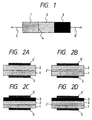
- Fig. 1 is a schematic cross sectional view showing the most conceptual element structure of an explanatory light emitting device not according to the present invention.
- the light emitting device has a structure where the luminous region 2 comprising a luminous porous material is sandwiched between the current injection electrode regions 1, 3.
- the injection electrode region 1 is formed of a non-porous material with a low resistance which is same as the mother material for the luminous region 2.
- the interface 4 between both the regions has a continuous crystal structure. Both the regions have a different conductivity type from each other, and homogeneous pn-type junction is formed there.
- the injection electrode region 3 does not depend on its structure if it is of a low resistance.
- the injection electrode region 3 has the same conductivity type as that of the luminous region 2.
- the interface between both the regions has a continuous crystal structure.
- a DC current is conducted between the injection electrode regions 1 and 3 via the extracting electrode 5 and 5' connected to the device, electric charges are injected from the homogeneous pn-junction interface 4 to the luminous region 2 so that light emission occurs.
- the extracting electrode 5' is directly bonded to the light emitting region 2 with a low contact resistance, the injection electrode region 3 can be omitted.
- the explanatory light emitting device has a high efficiency by forming an injection electrode region which is in "non-porous structure", which has “a crystal structure” continuous to the luminous region 2, and which is of “the same material” and of “heterojunction-type".
- the injection electrode region 3 when the injection electrode region 3 is provided, (3) the contact between the luminous region 2 and the injection electrode region 3 is no matter because of "continuity of crystal structure", and (4) it is expected that the good ohmic contact between the injection electrode region 3 and the extracting electrode 5' results from the low resistivity of the injection electrode region 3.
- the luminous region 2 is made of an uniform luminous porous material along the whole region.
- the luminous region may be formed of plural porous or non-porous regions of different structure. It is required that at least one of the regions must be a luminous material. Therefore, if other regions are offered for other uses except the luminous function, both the device characteristics and the device manufacturing method may be convenient in some cases.
- the vicinity of the interface of the injection electrode region 1 is made non-porous or non-luminous porous material having relatively large residual structure, whereby the pn-junction can further be improved at the interface 4.
- the method which uses an epitaxial growth can further improve the epitaxial interface and the film quality of an epitaxial layer.
- the structure is formed of the same mother material as the injection electrode region 1 or 3, whereby it is not important that a hetero-material may be formed on the surfaces facing pores in the residual structure. Moreover, all spaces in a pore may be filled with a hetero-material. Generally, in some cases, the mechanical and thermal stability is not enough because the luminous porous material has a very fine residual structure. Hence, in some cases, an effective reinforcement may be made using the above hetero-material.
- Figs. 2A to 2D illustrate a spatial arrangement of a luminous region comprising a non-porous region and a luminous porous material.
- Figs. 2B and 2C illustrate embodiments of a light emitting device according to the present invention.
- Figs. 2A to 2D show an example where a current route is vertically formed on the surface of a monocrystalline substrate in a wafer form.
- a pn-junction is formed between the non-porous layer 1 of a first conductivity type and the luminous porous layer 2 of a second conductivity type, with a continuous crystal structure in the pn-junction.
- the extracting electrodes 5 and 5' are provided on the ends of the element structure, respectively.
- Like numerals represent regions corresponding to those in Fig. 1.
- the intermediate layer 2' is arranged between the nonporous layer 1 and the luminous porous layer 2 (Fig. 2B).
- the luminous region 2 includes an region other than the luminous porous region in the structure shown in Fig. 1. That is, the intermediate layer 2' includes the luminous region 2 shown in Fig. 1.
- the intermediate region 2' comprises a non-porous material including monocrystal.
- the conductive type of the intermediate region 2' is the same as that of the luminous porous layer 2, and the layers on the front and back of the intermediate layer 2' should be continued in crystal structure.
- it is not necessarily needed that the interface between the intermediate layer 2' and other layer in the luminous region 2 is sharp, but it may be varied restrictively and continuously.
- an additional injection electrode layer 3 may be provided (Fig. 2C).
- Fig. 2C This is an explanatory example showing the injection electrode 3 which is provided in the device structure shown in Fig. 1.
- the injection electrode layer 3 is formed of, for example, a non-luminous porous material or non-porous material including monocrystal.
- the conductivity type of the injection electrode layer 3 should be same as the luminous non-porous layer 2.
- the crystal structure between the injection electrode layer 3 and the luminous non-porous electrode layer 2 should be continued in crystal structure.
- the interface is not necessarily needed to be sharp, but may restrictively and continuously vary.
- Fig. 2D illustrates an embodiment of the invention comprising the injection electrode layer 3.
- Figs. 3A to 3D are explanatory examples and embodiments showing that an electrode route is formed in a direction parallel to a surface of noncrystal film provided on the insulating surface of, for example, the substrate in wafer form 0.
- Each structural element and its function correspond to those shown in Figs. 2A to 2D.
- the extracting electrodes 5 and 5' are in contact with the film surface.
- the geometric arrangement should not be limited to the present example.
- the device of an embodiment shown in Figs. 2A to 2D and 3A to 3D will be explained in accordance with a process for forming a light emitting region comprising a luminous porous material and a non-porous region each having a different conductivity type, so as to form a continuous crystal structure.
- the first explanatory method of manufacturing a device with the structure shown in Fig. 2A is shown in Figs. 4A to 4C.
- a non-porous substrate 1 having a desired conductivity type and a resistance is prepared (Fig. 4A).
- the layer 20 may be formed by epitaxial growth on the surface of the substrate 1 with impurity elements being introduced to control the conductivity type, or the layer 20 is internally formed from the surface of the substrate 1 by effecting counter-doping by an ion implantation from the surface of the substrate 1, a solid-phase diffusion from a deposited, or a diffusion from a gas-phase film.
- the luminous region 2 comprising a luminous porous material can be made by making the layer 20 porous from the surface to the interface 4 by using a method of converting a non-porous material into a porous material, such as anodization or a photo-formation (Fig. 4C).
- the extracting electrodes 5 and 5' are formed. Finally, a device with the structure shown in Fig. 2A can be formed. Since the pn-junction interface 4 has a continuous crystal structure before a porous structure formation, the original state is maintained even after a final step.
- a non-porous substrate 1 with a desired conductivity type and a desired resistance is prepared (Fig. 5A).
- a porous structure formation is effected from the surface of the substrate 1 to a desired depth (Fig. 5B).
- a counter doping is carried out from the surface of the porous structure formation layer 20 to make the luminous porous layer 2 having a different conductivity type from that of the substrate 1 (Fig. 5C).
- a device with the structure shown in Fig. 2A can be formed by forming the extracting electrodes 5 and 5'.
- the crystal structure needless to say, is continuous at the pn-junction interface 4.
- the intermediate layer 2' is left to a desired thickness by terminating porous structure formation just before the formation reaches the interface 4 from the surface of the layer 2 (Fig 6).
- a counter doping is effected over the surface of the porous structure formation layer 20 to the non-porous region of the substrate 1 to form the intermediate layer 2' having a desired thickness (Fig. 7).
- the intermediate layer 2' is made of a non-porous material of the same conductive type as that of the luminous porous layer 2 and has a continuous crystal structure at the pn-junction interface 4 to the substrate 1.
- the second explanatory method of manufacturing the device shown in Fig. 2B is not applied to the step in which a pn-junction is formed by counter-doping after the porous structure layer is formed as shown in Figs. 5A to 5C.
- the reason is that the phenomenon is utilized, that both the porous structure formation and the porous material structure are largely influenced by the composition of non-porous material, impurity concentration, and other factors.
- the structure strength increases because when a heavy impurity concentration in a silicon substrate lowers a resistance, the residual structure is large and the porous degree lowers, thus suppressing a resistance increase due to porous material. In this case, a non-luminous porous material is formed.
- a non-luminous porous material of low resistance is used as the intermediate layer 2' shown in Fig. 2B.
- the non-porous substrate 1 having a desired conductivity type and a resistance is prepared (Fig. 8A).
- the layer 20' which has conductivity type different from that of the substrate 1 but has the same mother material and has a continuous crystal structure at the interface 4, is provided.
- the layer 20, which has the same conductivity type as that of layer 20' but has a different impurity concentration and has a continuous crystal structure (Fig. 8B).
- the impurity concentration of the layer 20' may be set to a higher amount than that of the layer 20.
- the process used in the step shown in Fig. 4B can be used in the concrete method of manufacturing the layers 20 and 20'.
- layer 20 may be deposited after a deposition of the layer 20'.
- multiple step ion-implantation with varying implanting energy conditions or ion species, or an ion-implanting profile may be used, whereby the spatial transition between the layers 20 and 20' becomes continuous.
- the luminous region 2 comprising a luminous porous material, the layer 20' acting as the intermediate layer 2', is formed.
- the extracting electrodes 5, 5' are formed on the luminous region 2 to form a light emitting device with the structure shown in Fig. 2B. In this case, the crystal structure at the pn-junction interface is continuous.
- the first explanatory method of manufacturing a device with the structure shown in Fig. 2C is shown in Figs. 9A to 9C.
- the non-porous substrate 1 having a desired conductivity type and a resistance is prepared (Fig. 9A).
- the layer 20, which has a conductivity type different from that of the substrate 1 but has the same mother material and has a continuous crystal structure at the interface 4 is provided.
- the layer 30, which has the same conductivity type as that of the layer 20 and has a different impurity concentration is provided (Fig. 9B).
- the impurity concentration of the layer 30 may be higher than that of the layer 20.
- the formation is effected by epitaxial growth, the layer 30 is deposited after a deposition of the layer 20.
- multiple step ion-implantation with varying implanting energy conditions or ion species, or an ion-implanting profile may be used, whereby the spatial transition between the layers 20 and 30 becomes continuous.
- both the layers become an injection electrode layer 3 of a non-luminous porous material and the luminous layer 2 comprising a luminous porous material.
- the extracting electrodes 5 and 5' are formed on the luminous layer 2 to form a light emitting device with the structure shown in Fig. 2B. In this case, the crystal structure at the pn-junction interface 4 is continuous.
- the second explanatory method of manufacturing a device with the structure shown in Fig. 2C is shown in Figs. 10A to 10D.
- the non-porous substrate 1 having a desired conductivity type and a resistance is prepared (Fig. 10A).
- the layer 20, which has a conductivity type different from that of the substrate 1 but has the same mother material and has a continuous crystal structure at the interface 4 is provided (Fig. 10B).
- the concrete method of manufacturing the layer 20 is the same as the process described above.
- the layer 20 is made porous from the surface to the interface 4 to form the luminous layer 2 comprising a luminous porous material (Fig. 10C).
- the injection electrode layer 3 of a non-porous material is deposited on the surface by epitaxial growth etc. (Fig. 10D). Since the injection electrode layer 3 should be of the same conductivity type as that of the light emitting device 2 and have a low resistance, the impurities are introduced at a deposition or are doped in a later step.
- the injection electrode layer 3 of the plural layers shown in Fig. 11.
- the non-porous injection electrode layer 32 may be deposited by epitaxial growth etc. on the non-luminous porous injection electrode layer 31 formed according to the first method.
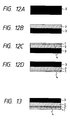
- the non-porous substrate 0 having a desired conductivity type and a resistance is prepared (Fig. 12A).
- the substrate 0 is made porous to a desired depth from the surface thereof to form the luminous layer 2 comprising a luminous porous material (Fig. 12B).
- the injection electrode layer 1 is deposited by epitaxial growth etc. on the surface of the substrate 0 (Fig. 12C). In this case, the injection electrode layer 1 should be of a non-porous material with a low resistance.
- the interface 4 between the injection electrode layer 1 and the luminous layer 2 should be a continuous crystal structure and the substrate 0 should be different from the luminous layer 2 in a conductivity type. Therefore, it is required that impurities are introduced at a deposition or are doped in a later step.
- Putting the substrate upside down makes the structure shown in Fig. 12D.
- the pn-junction interface 4 is formed between the injection electrode layer 1 finally deposited and the luminous layer 2.
- the injection electrode layer 3 which has the same conductivity as that of the luminous layer 2 in the substrate 0 left without being made porous is formed on the luminous layer 2.
- the extracting electrodes 5 and 5' are formed to obtain a device shown in Fig. 2C.
- the device shown in Fig. 2D can be formed by combining the method of manufacturing the device shown in Fig. 2B and the method of manufacturing the device shown in Fig. 2C.
- Fig. 2A after a layer which is of the same conductivity type as that of the substrate 0 and has a high impurity concentration is formed on the surface of the non-porous substrate 0, the process goes to the steps shown in Fig. 12B.
- the high impurity concentration layer is converted to the intermediate layer 2' of non-luminous porous material so that the structure shown in Fig. 13 is obtained and the device shown in Fig. 2D can be formed.
- the explanatory method of manufacturing the device group shown in Figs. 3A to 3D is the same as that shown in Figs. 2A to 2D except that a non-porous film on the insulating surface of a substrate is made porous.
- An explanation will be made as for some typical forming steps with reference to the device structure in Fig. 3D as an example.
- Figs. 14A to 14F show the first explanatory method of manufacturing the device in Fig. 3D.
- a substrate on which a non-porous film 20 is formed on the insulation surface of the substrate 0 is provided (Fig. 14A).
- the region 10 having a conductivity type different from that of the non-porous film 20 is formed in the non-porous film 20 and the region 30 having the same conductivity type as that of the non-porous film 20 and having a high impurity concentration and a high resistance is formed (Fig. 14B).
- the take-out electrodes 5 and 5' in contact with the regions 10 and 30, respectively, are formed using the patterning technique (Fig. 14C). Furthermore, a protective layer 6 is formed over the electrodes 5 and 5' (Fig. 14D). Since the protective layer 6 protects the structure underneath it in the following step when the region 20 of the remaining non-porous film is subjected to a porous structure forming process, it must sufficiently withstand against the porous structure forming process. The protective film 6 on the left end of the opening is offset from the boundary between the regions 10 and 20 as shown in the drawing. Next, the region 20 is converted into a porous layer. In the case where an anodizing process is used as a concrete porous structure forming process, the entire substrate is immersed in an electrolytic solution.
- the porous structure forming process is carried out merely by illuminating uniform rays.
- the region underneath the opening in the protective film 6 is converted into the luminous region 2 including a luminous porous material
- the offset part is converted into the intermediate layer 2'
- the regions 10 and 30 respectively converted into the injection electrode regions 1 and 3.
- the device shown in Fig. 3D having a pn-junction at the interface 4 with a continuous crystal structure is formed (Fig. 14F). If the offset of the protective film 6 at the opening is omitted, the device shown in Fig. 3C is formed. If formation of the region 30 is omitted, the device shown in Fig. 3B is formed. If the offset at the opening in the protective film 6 and formation of the region 30 are omitted, the device shown in Fig. 3A is formed.
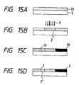
- a substrate comprising the non-porous film 20 formed on the substrate 0 having an insulation surface is provided (Fig. 15A).
- the entire substrate is immersed in an electrolytic solution.
- a photo-formation is carried out by illuminating a locally focused light 6 onto the non-porous film 20 to form the luminous region 20 including a luminous porous material (Fig. 15B).
- the region 10 having a conductivity type different from that of the non-porous film 20 and the region 30 having the same conductivity type as that of the non-porous film 20 and having a high impurity concentration and a low resistance are formed (Fig. 15C).
- the structure shown in Fig. 3D which includes the regions 10 and 30 respectively converted into the injection electrode regions 1 and 3 as well as the region remaining between the region 10 and the luminous region 2 converted into the intermediate layer 2', is formed (Fig. 15D).
- the devices shown in Figs. 3A to 3C can be formed by changing the spatial position of the region 10, or omitting some steps.
- a phosphorus-doped n-type silicon monocrystalline wafer which has a face orientation of ⁇ 100> and a resistivity of 0.02 ⁇ cm is prepared.
- a p-type monocrystalline silicon layer of a thickness of about 1 ⁇ m was epitaxially grown using a CVD process simultaneously using dichlorosilane gas and diborane gas.
- Aluminum of a film thickness of 200 nm (2000 ⁇ ) was vapor-deposited on the back surface of the wafer to ensure perfect ohmic contact.
- an SiO 2 film of a thickness of 200 nm (2000 ⁇ ) was again deposited on the wafer surface by using the CVD process. Then some 2 mm square openings were formed in the oxide film by the conventional photolithography process. In forming the openings, the oxide film on the top surface of the oxidized porous layer as the underlying layer must also be removed. Before a re-formation of a natural oxide film in the opening, a semi-transparent gold thin film of a film thickness of 10 nm (100 ⁇ ) was deposited thereto. Moreover, an Al extracting electrode was wired from the opening.
- a device was prepared by repeating the device preparation steps of Comparative Example 1 with the exception that the anodization time in was reduced by 1.5 seconds.
- the cross section of a sample particularly prepared to confirm the porous structure formation was observed under an electron microscope with a high resolving power, it was confirmed that the anodization advances from the wafer surface up to about 0.9 ⁇ m depth to form a porous layer, and that the lattice image was perfectly in a continuous state but a monocrystalline intermediate layer about 0.1 ⁇ m thick was formed between a contrast producing surface which appeared to be an epitaxial interface and a porous layer.
- the device When a DC voltage was applied between the contacts on the front and back surfaces of a wafer, the device showed a rectification ratio which is higher by nearly one order than that of the device of Comparative Example 1.
- the threshold voltage increased slightly to about 3.5 volts but a luminous efficiency was obtained which was several times stronger than that of the device of Comparative Example 1. It is presumed that the improved rectification characteristic results from that the front and back portions of the pn-junction are formed of a perfect monocrystal. This improves the efficiency of current injection into the luminous porous layer, thus increasing the luminous efficiency.
- a device was prepared by repeating the device preparation steps of Comparative Example 1 with the exception that the step of growing a p-type epitaxial layer on an n-type monocrystalline substrate was divided into two steps.
- the two steps for forming a p-type layer comprised depositing a heavily doped layer about 0.2 ⁇ m thick with the partial pressure of diborane gas increased ten times and then reducing the diborane gas partial pressure to the original pressure to grow a lightly doped layer about 0.2 ⁇ m thick.
- a boron-doped p-type silicon monocrystalline wafer having a face orientation of ⁇ 100> and a resistivity of 10 ⁇ cm was prepared. Boron ions were accelerated at 50 keV to be implanted into the back surface of the wafer with a dose of 5 x 10 14 cm -2 . Then the wafer was subjected to a thermal annealing at 950°C for 30 minutes in nitrogen atmosphere to be activated.
- the substrate was arranged between a pair of parallel platinum plane electrodes and immersed in a hydrofluoric acid ⁇ ethanol solution of a concentration of 25 wt%.
- Anodization was performed by applying a DC voltage between one platinum electrode acting as an anode electrode facing the back surface of the wafer and the other platinum electrode for one minute, with the region other than the wafer surface being electrically insulated, while the current density on the wafer surface was controlled to 10 mA ⁇ cm -2 .
- the wafer was left for 10 minutes under a lighting in a room, with the active circuit electrically shortcircuited.
- the oxide film on the top surface of the porous layer was removed with a dilute aqueous hydrofluoric acid solution.
- ITO was vapor-deposited to a thickness of 150 nm (1500 ⁇ ) and then patterned in 5 mm square in the fashion of islands.
- An AlSi film was deposited on the entire back surface of the wafer by sputtering.
- a device was prepared by following the procedure of Comparative Example 2 with the exception that the accelerating energy for the hydrogen ion implantation was boosted to 45 keV and the dose amount was doubled. Although it is difficult to clearly determine by a cross section observation, it is presumed that the n-type region extends to the inside of the monocrystalline substrate through the porous layer.
- the device When a DC current was conducted between the electrodes on the front and back surfaces of the wafer, the device indicated a rectification ratio being higher by nearly one order than the device of Comparative Example 2.
- the threshold voltage increased slightly to about 6 volts, but the luminous efficiency as obtained was several times stronger than that in Comparative Example 2. It is presumed that the improved rectification characteristic results from that the front and back regions of the pn-junction interface is formed of a perfect monocrystal and that this improves the efficiency of current injection into the luminous porous layer, thus increasing the luminous efficiency.
- a device was prepared by following the procedure of Comparative Example 1 with the exception that after a p-type epitaxial layer had been grown on an n-type monocrystalline substrate, boron ions were implanted into the surface thereof at an accelerating voltage of 20 keV with a dose of 5 x 10 14 cm -2 and the substrate was subjected to thermal annealing in a nitrogen atmosphere at 950 °C for 30 minutes to be activated.
- An observation of the cross section of a sample found that the anodization advances from the wafer surface up to about 1 ⁇ m depth to form a porous layer.
- the surface was of a porous layer having large pores and a thickness of about 0.05 ⁇ m and the underlying lower porous layer was almost of a ultra-fine porous layer.
- both the rectification characteristic and the luminous threshold voltage were substantially the same as those in Comparative Example 1 and the luminous efficiency was improved several times that in Comparative Example 1.
- the porous layer with large pore structure on the outer surface acts as the injection electrode layer 3 shown in Fig. 2C, the contact resistance with the extracting electrode is reduced so that the luminous efficiency is improved.
- a device was prepared by following the procedure of Comparative Example 1 with the exception that the following step was added between the RTO treatment to the porous layer and the CVD-SiO 2 layer deposition step.
- the added step includes removing the oxide film on the top surface of the porous layer with the oxidized surface of the residual structure, and then epitaxially growing a p-type silicon layer of 30 nm (300 ⁇ ) thickness by using a bias sputtering method in which a heavily doped p-type silicon target is used.
- a bias sputtering method in which a heavily doped p-type silicon target is used.
- a device was prepared by following the procedure of Comparative Example 3 with the exception that the following step was added after the porous layer forming step and the RTO treating step.
- the added step is a step of, after an oxide film had been removed, epitaxially growing, a p-type silicon layer of about 15 nm (150 ⁇ ) thick by using a bias sputtering method where a p-type silicon with a high concentration was used as a target.
- an ultra-thin layer of about 0.05 ⁇ m in depth in the top surface side of the porous layer was converted to a porous structure with coarse pores.
- the epitaxial layer on the porous layer is nearly a monocrystal because a defect or the like was not found therein. It is considered that the improved crystallinity of the epitaxial layer results from that the epitaxial growth surface is a porous with coarse pores, compared with that in Comparative Example 4.
- the rectification characteristics of the device was substantially the same as those in Comparative Example 3.
- the luminous threshold voltage was slightly increased, whereby the luminous efficiency was improved by about 50%.
- the epitaxial layer on the top surface as well as the underlying porous layer with a coarse structure act as the injection electrode layer 3 shown in Fig. 2C, it is considered that the contact resistance of the take-out electrode is reduced so that the luminous efficiency is improved.
- an about 200 nm (2000 ⁇ ) thick SiO 2 film was again deposited on the surface of the wafer by using a CVD process.
- some openings of 2 x 2 mm 2 were formed in the oxide film.
- a semi-transparent gold film of a thickness of 10 nm (100 ⁇ ) was vapor-deposited in the openings to wire the take-out electrodes A1 derived from the openings.
- the device produced by the above steps indicated a rectification characteristic in which a forward current flows to the surface electrode acting as a cathode electrode.
- An area light emission of nearly orange visible rays was emitted from the openings in the oxide film at a threshold voltage of about 2 volts. It is considered that this light emission is due to an electroluminescence based on a current injection to the porous silicon layer with the ultra-fine structure via the junction interface between the n-type epitaxial crystal layer and the underlying p-type porous layer. It is presumed that the sufficiently low luminous threshold voltage for practical use results from that the pn-junction interface has a continuous crystal structure and a good rectification characteristics and therefore the current injection efficiency is very high.
- the device was prepared by a method not according to the invention in the same manner as in the Comparative Example 6 except that before converting the surface of a p-type monocrystalline substrate into a porous structure, boron ions with a dose of 5 x 10 14 cm -2 were implanted to the surface thereof at an accelerating voltage of 20 keV. Then the implanted surface was activated by annealing in a nitrogen atmosphere at 950°C for 30 minutes. An observation of the cross section of a sample found that the ultra-thin layer of about 0.05 pm in the top surface side of the porous layer was in a porous state with bulky structure and that the epitaxial layer thereon included nearly no defects, and it can be stated that it is nearly a monocrystal. It is considered that the epitaxial layer having a crystallinity better than that in the Comparative Example 4 results from the epitaxially grown surface with bulky porous structure.
- the rectification characteristics and luminous threshold voltage of the device were substantially the same as those in the Comparative Example 6 and the luminous efficiency was improved several times, compared with that in the Comparative Example 6. In this case, it is considered that the crystallinity of the n-type epitaxial silicon layer in the top surface reduced the contact resistance of the interface so that the luminous efficiency was improved.
- a SOI substrate having a boron-doped p-type silicon monocrystalline thin film with a face orientation of ⁇ 100> and a thickness of 0.5 ⁇ m formed on a transparent quartz substrate was provided.
- the SOI substrate was subjected to the LOCOS process to form 10 x 10 ⁇ m 2 element separation regions.
- the surfaces of the separated silicon islands were oxidized to about 50 nm (500 ⁇ ).
- boron ions accelerated at 150 keV were implanted with a dose of 2 x 10 15 cm -2 into the right region and phosphorus ions accelerated at 150 keV were implanted with a dose of 3 x 10 15 cm -2 into the left region.
- the substrate was subjected to a thermal annealing in a nitrogen atmosphere at 950 °C for 30 minutes to activate it.
- aluminum wirings were formed in contact with the right and left ion implanted regions. Particularly, the wiring from the boron implanted region was wound to the orientation flat of the substrate. Then a conventional photoresist was coated on the surface of the substrate.
- An opening was formed in the non ion-implanted stripe region left at the middle area of the silicon island at the surface side.
- the end of the opening at the pn-junction side was offset so as to overlap slightly the inner side of the stripe region from the junction boundary. Then the oxide film on the surface in the opening was removed.
- the substrate was subjected to an anodizing process by immersing in a hydrofluoric acid-ethanol solution of a concentration of 25 wt ⁇ % while a direct current was conducted between a platinum plate electrode acting as a cathode facing the substrate and the aluminum wirings winding to the orientation flat of the substrate.
- the anodizing process was completed in 30 seconds while the anodizing current density was controlled at a fixed value of about 20 mA ⁇ cm -2 at the photoresist opening on the surface of the substrate. Then the photoresist was removed from the substrate.
- a SiNx film was deposited on the entire surface of the substrate by using a plasma CVD process. An opening was formed at a portion where the aluminum wiring was needed.
- the device On conducting a direct current between two electrodes sandwiching the porous region in the device, the device indicated its good rectification characteristics. A luminescence was recognized from a small applied voltage of about 1 volt.
- an SIMOX substrate having a phosphorus-doped n-type silicon monocrystalline thin film with a face orientation of ⁇ 100>, a resistivity of 20 ⁇ cm, and a thickness of 0.5 ⁇ m formed on a buried oxide film of 300 nm (3000 ⁇ ) thick was provided.
- the SIMOX substrate was immersed in a hydrofluoric acid solution of a concentration of 49 wt ⁇ %.
- a photo-formation was carried out by irradiating a He-Ne laser beam focused in a rectangular shape of 2 x 8 ⁇ m 2 onto a part of the substrate surface for 30 minutes.
- the substrate was subjected to the RTO process to stabilize the porous region.
- an ion implantation was performed to the two regions sandwiching the porous region to isolate electrically them.
- the element separation step using the LOCOS process activates the implanted ions.
- the phosphorus ion-implanted region was spaced from the porous region by 0.1 ⁇ m and the boron ion-implanted region was spaced from the porous region by 0.2 ⁇ m.
- the horizontal diffusion during an activation annealing was ceased at or just before the boundary of the porous region.
- An intermediate layer was formed between the boron implanted region and the porous region.
- aluminum wirings were derived out of both the ion implanted regions so that a device was completely formed.
- a SOI substrate having a boron-doped p-type silicon monocrystalline film 200 with a face orientation of ⁇ 100>, a resistivity of 10 ⁇ cm, and a thickness of 0.5 ⁇ m formed on an insulation surface of a silicon substrate 0 was provided (Fig. 16A).
- the substrate was subjected to an element isolation by using the LOCOS process to form island regions 20 each having an area of 10 x 10 ⁇ m 2 .
- a 50 nm (500 ⁇ ) thick oxide film 7 was formed on the surface of each isolated silicon island by using a thermal oxidizing process (Fig. 16B).
- a polycrystalline silicon film of 0.5 ⁇ m thick was deposited on the surface of the oxide film 7 by using the LPCVD process.
- the polycrystalline silicon film was patterned through a conventional photolithography process so as to leave the 2 ⁇ m wide island region 8 (Fig. 16C). Then, with the photoresist acting as a patterned mask, phosphorus ions with a dose of 2 x 10 15 cm -2 accelerated at 180 keV were locally implanted to the polycrystalline silicon film island region 8 as well as the parts 10 and 10' of the silicon monocrystalline film island region 20 at the both sides of the region 8. Moreover, boron ions with a dose of 1 x 10 15 cm -2 accelerated at 100 keV were implanted to a part 30 of the silicon monocrystalline film island region 20 by using the above step (Fig. 16D).
- the impurities were activated by a thermal process at 900°C for 30 minutes.
- the oxide films on the surfaces of the regions 30 and 10' were removed, and then aluminum wirings 5 and 5' were taken out of the openings (Fig. 16E).
- the silicon oxide film 9 was deposited on the surface of the resultant substrate and the aluminum wiring 50 was taken out to conduct to the silicon monocrystalline film island region 9 (Fig. 17A).
- the opening 100 was formed on a part of the upper part of the silicon monocrystalline film island 20 (Fig. 17B).
- the silicon nitride film 6 was formed so as to leave an opening of 1.5 ⁇ m wide with a slight offset to the region 10 (Fig. 17C).
- the region 2 opened in the same way as that in the Example 11 was converted to a porous layer.
- a light emitting device which includes the regions 10 and 30 corresponding to the ion-implanted electrode regions 1 and 3 shown in Fig. 14F, the region 2 corresponding to the porous region 2 including a light emitting region, and the offset region corresponding to the intermediate region 2' was formed according to the above steps (Fig. 17D).
- the ion-implanted electrode region 1 acts as the drain region of a MOS transistor including the region 10' acting as a source part, the region 20 acting as a channel part, and the polycrystalline silicon film island region 9 acting as a gate electrode. With a voltage of 15 volts applied between the wirings 5 and 5', when the gate voltage was increased from 0 via the wiring 50, the MOS transistor was turned on at a threshold voltage 1.1 volts.
- the porous region including a light emitting region glowed at 1.5 volts and more.
- the relationship between the luminous intensity and gate voltage indicated linear characteristics over 2 volts.
- a light emitting device has a device constitution comprising a non-porous region having a continuous crystal structure adjacent to the luminous region including a porous material and acting as a current injection electrode to the luminous region, whereby the perfect adhesive property between the electrode and the luminous region reduces the contact resistance.
- a current injection from the junction portion could be injected with high efficiency.
- the light emitting device manufacturing method can provide light emitting devices with good luminous efficiency.
Abstract
Description
Claims (6)
- A light emitting device comprising a luminous region (2) comprising a porous semiconductor having a first conductivity type, a contact region (1) comprising a non-porous semiconductor having a second conductivity type and being electrically connected to the luminous region (2), and an electrode (5) provided at the contact region, the luminous region being light-emitting as a result of a current flowing into the luminous region through the contact region,
characterized in that
an intermediate region (2') comprising a non-porous semiconductor of a first conductivity type is provided between the luminous region (2) and the contact region (1) and that the current flows into the luminous region through the intermediate region (2'). - The light emitting device according to claim 1, wherein the luminous region (2), the intermediate region (2') and the contact region (1) form successive layers.
- The light emitting device according to claim 1, wherein the luminous region (2), the intermediate region (2') and the contact region (1) are formed on the same substrate and are parallel to a surface of the substrate.
- The light emitting device according to claim 1, wherein the luminous region (2) and the intermediate region (2') comprise a p-type silicon and the contact region (1) comprises an n-type silicon.
- A method for manufacturing a light emitting device according to claim 2, comprising the steps of:epitaxially growing a p-type silicon layer (2, 2') on an n-type silicon substrate (1);causing a part of the p-type silicon layer (2) in the thickness direction to be made porous; andproviding the n-type silicon substrate (1) and the p-type silicon layer (2) having been made porous with an electrode (5, 5').
- The method according to claim 5, wherein the porous structure formation is conducted by anodization.
Applications Claiming Priority (4)
| Application Number | Priority Date | Filing Date | Title |
|---|---|---|---|
| JP6993893 | 1993-03-29 | ||
| JP69938/93 | 1993-03-29 | ||
| JP4902294A JPH06338631A (en) | 1993-03-29 | 1994-03-18 | Light-emitting element and manufacture thereof |
| JP49022/94 | 1994-03-18 |
Publications (3)
| Publication Number | Publication Date |
|---|---|
| EP0618624A2 EP0618624A2 (en) | 1994-10-05 |
| EP0618624A3 EP0618624A3 (en) | 1995-05-31 |
| EP0618624B1 true EP0618624B1 (en) | 1998-12-02 |
Family
ID=26389374
Family Applications (1)
| Application Number | Title | Priority Date | Filing Date |
|---|---|---|---|
| EP94104882A Expired - Lifetime EP0618624B1 (en) | 1993-03-29 | 1994-03-28 | Light emitting device and method of manufacturing the same |
Country Status (5)
| Country | Link |
|---|---|
| US (1) | US5726464A (en) |
| EP (1) | EP0618624B1 (en) |
| JP (1) | JPH06338631A (en) |
| AT (1) | ATE174156T1 (en) |
| DE (1) | DE69414898T2 (en) |
Families Citing this family (23)
| Publication number | Priority date | Publication date | Assignee | Title |
|---|---|---|---|---|
| US7148119B1 (en) | 1994-03-10 | 2006-12-12 | Canon Kabushiki Kaisha | Process for production of semiconductor substrate |
| GB2299204A (en) | 1995-03-20 | 1996-09-25 | Secr Defence | Electroluminescent device |
| CN1132223C (en) | 1995-10-06 | 2003-12-24 | 佳能株式会社 | Semiconductor substrate and producing method thereof |
| TW391022B (en) * | 1997-10-29 | 2000-05-21 | Mitsubishi Rayon Co | Field emission electron source, method of producing the same, and use of the same |
| JP3413090B2 (en) | 1997-12-26 | 2003-06-03 | キヤノン株式会社 | Anodizing apparatus and anodizing method |
| DE59807589D1 (en) * | 1998-02-10 | 2003-04-24 | Infineon Technologies Ag | OPTICAL STRUCTURE AND METHOD FOR THE PRODUCTION THEREOF |
| US6455344B1 (en) * | 1998-05-19 | 2002-09-24 | National Science Council | Method of fabricating a planar porous silicon metal-semicoductor-metal photodetector |
| KR100338140B1 (en) * | 1998-09-25 | 2002-05-24 | 이마이 기요스케 | Electric field emission type electron source |
| JP2000277478A (en) | 1999-03-25 | 2000-10-06 | Canon Inc | Anodization device and system, substrate processing device and method, and manufcature thereof |
| US6410436B2 (en) | 1999-03-26 | 2002-06-25 | Canon Kabushiki Kaisha | Method of cleaning porous body, and process for producing porous body, non-porous film or bonded substrate |
| US6468923B1 (en) | 1999-03-26 | 2002-10-22 | Canon Kabushiki Kaisha | Method of producing semiconductor member |
| CN1311874C (en) * | 2002-07-11 | 2007-04-25 | 住友电气工业株式会社 | Porous semiconductor and process for producing the same |
| JP4438049B2 (en) * | 2003-08-11 | 2010-03-24 | キヤノン株式会社 | Field effect transistor, sensor using the same, and manufacturing method thereof |
| US7294323B2 (en) * | 2004-02-13 | 2007-11-13 | Battelle Energy Alliance, Llc | Method of producing a chemical hydride |
| US7112455B2 (en) * | 2004-06-10 | 2006-09-26 | Freescale Semiconductor, Inc | Semiconductor optical devices and method for forming |
| US7514859B2 (en) * | 2004-12-20 | 2009-04-07 | Hewlett-Packard Development Company, L.P. | Ultraviolet emitter display apparatus |
| JP5110803B2 (en) * | 2006-03-17 | 2012-12-26 | キヤノン株式会社 | FIELD EFFECT TRANSISTOR USING OXIDE FILM FOR CHANNEL AND METHOD FOR MANUFACTURING THE SAME |
| JP5003013B2 (en) * | 2006-04-25 | 2012-08-15 | 株式会社日立製作所 | Silicon light-emitting diode, silicon phototransistor, silicon laser, and manufacturing method thereof. |
| JP4920342B2 (en) * | 2006-08-24 | 2012-04-18 | 浜松ホトニクス株式会社 | Method for manufacturing silicon element |
| JP4920343B2 (en) * | 2006-08-24 | 2012-04-18 | 浜松ホトニクス株式会社 | Semiconductor element |
| US8399995B2 (en) * | 2009-01-16 | 2013-03-19 | Infineon Technologies Ag | Semiconductor device including single circuit element for soldering |
| US8260098B1 (en) * | 2011-02-17 | 2012-09-04 | Nxp B.V. | Optocoupler circuit |
| ITUB20152264A1 (en) * | 2015-07-17 | 2017-01-17 | St Microelectronics Srl | DEVICE FOR EMISSION OF LIGHT IN POROUS SILICON AND ITS RELATED MANUFACTURING METHOD |
Family Cites Families (5)
| Publication number | Priority date | Publication date | Assignee | Title |
|---|---|---|---|---|
| DE4126955C2 (en) * | 1991-08-14 | 1994-05-05 | Fraunhofer Ges Forschung | Process for the production of electroluminescent silicon structures |
| US5285078A (en) * | 1992-01-24 | 1994-02-08 | Nippon Steel Corporation | Light emitting element with employment of porous silicon and optical device utilizing light emitting element |
| DE4231310C1 (en) * | 1992-09-18 | 1994-03-24 | Siemens Ag | Process for the production of a component with porous silicon |
| US5298767A (en) * | 1992-10-06 | 1994-03-29 | Kulite Semiconductor Products, Inc. | Porous silicon carbide (SiC) semiconductor device |
| US5324965A (en) * | 1993-03-26 | 1994-06-28 | The United States Of America As Represented By The Secretary Of The Army | Light emitting diode with electro-chemically etched porous silicon |
-
1994
- 1994-03-18 JP JP4902294A patent/JPH06338631A/en active Pending
- 1994-03-28 DE DE69414898T patent/DE69414898T2/en not_active Expired - Fee Related
- 1994-03-28 AT AT94104882T patent/ATE174156T1/en not_active IP Right Cessation
- 1994-03-28 EP EP94104882A patent/EP0618624B1/en not_active Expired - Lifetime
-
1996
- 1996-06-27 US US08/670,150 patent/US5726464A/en not_active Expired - Fee Related
Also Published As
| Publication number | Publication date |
|---|---|
| DE69414898D1 (en) | 1999-01-14 |
| ATE174156T1 (en) | 1998-12-15 |
| DE69414898T2 (en) | 1999-06-10 |
| EP0618624A3 (en) | 1995-05-31 |
| US5726464A (en) | 1998-03-10 |
| EP0618624A2 (en) | 1994-10-05 |
| JPH06338631A (en) | 1994-12-06 |
Similar Documents
| Publication | Publication Date | Title |
|---|---|---|
| EP0618624B1 (en) | Light emitting device and method of manufacturing the same | |
| EP0584777B1 (en) | Semiconductor device and process for producing the same | |
| US5247533A (en) | Gallium nitride group compound semiconductor laser diode | |
| JP2666237B2 (en) | Group III nitride semiconductor light emitting device | |
| US3922703A (en) | Electroluminescent semiconductor device | |
| CA2054242C (en) | Light-emitting semiconductor device using gallium nitride group compound | |
| JPH04312982A (en) | Semiconductor polycrystalline diamond electronic device and manufacture thereof | |
| JP3654738B2 (en) | Group 3 nitride semiconductor light emitting device | |
| KR20010079918A (en) | Semiconductor substrate and its production method, semiconductor device comprising the same and its production method | |
| US6017773A (en) | Stabilizing process for porous silicon and resulting light emitting device | |
| JP2001015852A (en) | Electrode structure of p-type group iii nitride semiconductor layer and method for forming the same | |
| EP0312466B1 (en) | Process of manufacturing a silicon structure on isolator | |
| KR100289595B1 (en) | Group III-nitride semiconductor light emitting device | |
| KR20050035325A (en) | Nitride semiconductor light emitting device and method of manufacturing the same | |
| JP2999591B2 (en) | Method for manufacturing GaAs device having high-purity intrinsic layer | |
| JP3693436B2 (en) | Light emitting device grown on ZnSe substrate | |
| KR100361696B1 (en) | Schottky Barrier Diode and its manufacturing method | |
| US20040104384A1 (en) | Growth of high temperature, high power, high speed electronics | |
| Mimura et al. | Si-based optical devices using porous materials | |
| KR100317606B1 (en) | Method for fabricating Schottky barrier diode | |
| CN117253900A (en) | Luminance self-adaptive light-emitting diode and preparation method thereof | |
| JPS61268079A (en) | Blue light-emitting element | |
| Kubota et al. | Photoconductivity of hydrogenated amorphous GaP/chrystalline GaP junction | |
| JP2993654B2 (en) | Electrode structure | |
| JPH10242520A (en) | Gallium nitride compound semiconductor element and its manufacture |
Legal Events
| Date | Code | Title | Description |
|---|---|---|---|
| PUAI | Public reference made under article 153(3) epc to a published international application that has entered the european phase |
Free format text: ORIGINAL CODE: 0009012 |
|
| AK | Designated contracting states |
Kind code of ref document: A2 Designated state(s): AT BE CH DE DK ES FR GB GR IE IT LI LU MC NL PT SE |
|
| PUAL | Search report despatched |
Free format text: ORIGINAL CODE: 0009013 |
|
| AK | Designated contracting states |
Kind code of ref document: A3 Designated state(s): AT BE CH DE DK ES FR GB GR IE IT LI LU MC NL PT SE |
|
| 17P | Request for examination filed |
Effective date: 19951016 |
|
| 17Q | First examination report despatched |
Effective date: 19961202 |
|
| GRAG | Despatch of communication of intention to grant |
Free format text: ORIGINAL CODE: EPIDOS AGRA |
|
| GRAG | Despatch of communication of intention to grant |
Free format text: ORIGINAL CODE: EPIDOS AGRA |
|
| GRAH | Despatch of communication of intention to grant a patent |
Free format text: ORIGINAL CODE: EPIDOS IGRA |
|
| GRAH | Despatch of communication of intention to grant a patent |
Free format text: ORIGINAL CODE: EPIDOS IGRA |
|
| GRAA | (expected) grant |
Free format text: ORIGINAL CODE: 0009210 |
|
| AK | Designated contracting states |
Kind code of ref document: B1 Designated state(s): AT BE CH DE DK ES FR GB GR IE IT LI LU MC NL PT SE |
|
| PG25 | Lapsed in a contracting state [announced via postgrant information from national office to epo] |
Ref country code: NL Free format text: LAPSE BECAUSE OF FAILURE TO SUBMIT A TRANSLATION OF THE DESCRIPTION OR TO PAY THE FEE WITHIN THE PRESCRIBED TIME-LIMIT Effective date: 19981202 Ref country code: LI Free format text: LAPSE BECAUSE OF FAILURE TO SUBMIT A TRANSLATION OF THE DESCRIPTION OR TO PAY THE FEE WITHIN THE PRESCRIBED TIME-LIMIT Effective date: 19981202 Ref country code: IT Free format text: LAPSE BECAUSE OF FAILURE TO SUBMIT A TRANSLATION OF THE DESCRIPTION OR TO PAY THE FEE WITHIN THE PRE;WARNING: LAPSES OF ITALIAN PATENTS WITH EFFECTIVE DATE BEFORE 2007 MAY HAVE OCCURRED AT ANY TIME BEFORE 2007. THE CORRECT EFFECTIVE DATE MAY BE DIFFERENT FROM THE ONE RECORDED.SCRIBED TIME-LIMIT Effective date: 19981202 Ref country code: GR Free format text: LAPSE BECAUSE OF NON-PAYMENT OF DUE FEES Effective date: 19981202 Ref country code: ES Free format text: THE PATENT HAS BEEN ANNULLED BY A DECISION OF A NATIONAL AUTHORITY Effective date: 19981202 Ref country code: CH Free format text: LAPSE BECAUSE OF FAILURE TO SUBMIT A TRANSLATION OF THE DESCRIPTION OR TO PAY THE FEE WITHIN THE PRESCRIBED TIME-LIMIT Effective date: 19981202 Ref country code: BE Free format text: LAPSE BECAUSE OF FAILURE TO SUBMIT A TRANSLATION OF THE DESCRIPTION OR TO PAY THE FEE WITHIN THE PRESCRIBED TIME-LIMIT Effective date: 19981202 Ref country code: AT Free format text: LAPSE BECAUSE OF FAILURE TO SUBMIT A TRANSLATION OF THE DESCRIPTION OR TO PAY THE FEE WITHIN THE PRESCRIBED TIME-LIMIT Effective date: 19981202 |
|
| REF | Corresponds to: |
Ref document number: 174156 Country of ref document: AT Date of ref document: 19981215 Kind code of ref document: T |
|
| REG | Reference to a national code |
Ref country code: CH Ref legal event code: EP |
|
| REF | Corresponds to: |
Ref document number: 69414898 Country of ref document: DE Date of ref document: 19990114 |
|
| REG | Reference to a national code |
Ref country code: IE Ref legal event code: FG4D |
|
| PG25 | Lapsed in a contracting state [announced via postgrant information from national office to epo] |
Ref country code: SE Free format text: LAPSE BECAUSE OF FAILURE TO SUBMIT A TRANSLATION OF THE DESCRIPTION OR TO PAY THE FEE WITHIN THE PRESCRIBED TIME-LIMIT Effective date: 19990302 Ref country code: PT Free format text: LAPSE BECAUSE OF FAILURE TO SUBMIT A TRANSLATION OF THE DESCRIPTION OR TO PAY THE FEE WITHIN THE PRESCRIBED TIME-LIMIT Effective date: 19990302 Ref country code: DK Free format text: LAPSE BECAUSE OF FAILURE TO SUBMIT A TRANSLATION OF THE DESCRIPTION OR TO PAY THE FEE WITHIN THE PRESCRIBED TIME-LIMIT Effective date: 19990302 |
|
| ET | Fr: translation filed | ||
| PG25 | Lapsed in a contracting state [announced via postgrant information from national office to epo] |
Ref country code: LU Free format text: LAPSE BECAUSE OF NON-PAYMENT OF DUE FEES Effective date: 19990328 Ref country code: IE Free format text: LAPSE BECAUSE OF NON-PAYMENT OF DUE FEES Effective date: 19990328 |
|
| NLV1 | Nl: lapsed or annulled due to failure to fulfill the requirements of art. 29p and 29m of the patents act | ||
| REG | Reference to a national code |
Ref country code: CH Ref legal event code: PL |
|
| PG25 | Lapsed in a contracting state [announced via postgrant information from national office to epo] |
Ref country code: MC Free format text: LAPSE BECAUSE OF NON-PAYMENT OF DUE FEES Effective date: 19990930 |
|
| PLBE | No opposition filed within time limit |
Free format text: ORIGINAL CODE: 0009261 |
|
| STAA | Information on the status of an ep patent application or granted ep patent |
Free format text: STATUS: NO OPPOSITION FILED WITHIN TIME LIMIT |
|
| 26N | No opposition filed | ||
| REG | Reference to a national code |
Ref country code: IE Ref legal event code: MM4A |
|
| REG | Reference to a national code |
Ref country code: GB Ref legal event code: IF02 |
|
| PGFP | Annual fee paid to national office [announced via postgrant information from national office to epo] |
Ref country code: FR Payment date: 20050308 Year of fee payment: 12 |
|
| PGFP | Annual fee paid to national office [announced via postgrant information from national office to epo] |
Ref country code: GB Payment date: 20050323 Year of fee payment: 12 |
|
| PGFP | Annual fee paid to national office [announced via postgrant information from national office to epo] |
Ref country code: DE Payment date: 20050324 Year of fee payment: 12 |
|
| PG25 | Lapsed in a contracting state [announced via postgrant information from national office to epo] |
Ref country code: GB Free format text: LAPSE BECAUSE OF NON-PAYMENT OF DUE FEES Effective date: 20060328 |
|
| PG25 | Lapsed in a contracting state [announced via postgrant information from national office to epo] |
Ref country code: DE Free format text: LAPSE BECAUSE OF NON-PAYMENT OF DUE FEES Effective date: 20061003 |
|
| GBPC | Gb: european patent ceased through non-payment of renewal fee |
Effective date: 20060328 |
|
| REG | Reference to a national code |
Ref country code: FR Ref legal event code: ST Effective date: 20061130 |
|
| PG25 | Lapsed in a contracting state [announced via postgrant information from national office to epo] |
Ref country code: FR Free format text: LAPSE BECAUSE OF NON-PAYMENT OF DUE FEES Effective date: 20060331 |