EP0622155A1 - Polishing pad and a method of polishing a semiconductor substrate - Google Patents
Polishing pad and a method of polishing a semiconductor substrate Download PDFInfo
- Publication number
- EP0622155A1 EP0622155A1 EP94104688A EP94104688A EP0622155A1 EP 0622155 A1 EP0622155 A1 EP 0622155A1 EP 94104688 A EP94104688 A EP 94104688A EP 94104688 A EP94104688 A EP 94104688A EP 0622155 A1 EP0622155 A1 EP 0622155A1
- Authority
- EP
- European Patent Office
- Prior art keywords
- region
- polishing pad
- polishing
- openings
- pore size
- Prior art date
- Legal status (The legal status is an assumption and is not a legal conclusion. Google has not performed a legal analysis and makes no representation as to the accuracy of the status listed.)
- Granted
Links
Images


Classifications
-
- B—PERFORMING OPERATIONS; TRANSPORTING
- B24—GRINDING; POLISHING
- B24B—MACHINES, DEVICES, OR PROCESSES FOR GRINDING OR POLISHING; DRESSING OR CONDITIONING OF ABRADING SURFACES; FEEDING OF GRINDING, POLISHING, OR LAPPING AGENTS
- B24B37/00—Lapping machines or devices; Accessories
- B24B37/11—Lapping tools
- B24B37/20—Lapping pads for working plane surfaces
- B24B37/26—Lapping pads for working plane surfaces characterised by the shape of the lapping pad surface, e.g. grooved
-
- B—PERFORMING OPERATIONS; TRANSPORTING
- B24—GRINDING; POLISHING
- B24B—MACHINES, DEVICES, OR PROCESSES FOR GRINDING OR POLISHING; DRESSING OR CONDITIONING OF ABRADING SURFACES; FEEDING OF GRINDING, POLISHING, OR LAPPING AGENTS
- B24B53/00—Devices or means for dressing or conditioning abrasive surfaces
- B24B53/017—Devices or means for dressing, cleaning or otherwise conditioning lapping tools
-
- Y—GENERAL TAGGING OF NEW TECHNOLOGICAL DEVELOPMENTS; GENERAL TAGGING OF CROSS-SECTIONAL TECHNOLOGIES SPANNING OVER SEVERAL SECTIONS OF THE IPC; TECHNICAL SUBJECTS COVERED BY FORMER USPC CROSS-REFERENCE ART COLLECTIONS [XRACs] AND DIGESTS
- Y10—TECHNICAL SUBJECTS COVERED BY FORMER USPC
- Y10S—TECHNICAL SUBJECTS COVERED BY FORMER USPC CROSS-REFERENCE ART COLLECTIONS [XRACs] AND DIGESTS
- Y10S451/00—Abrading
- Y10S451/921—Pad for lens shaping tool
Definitions
- the present invention relates to the field of semiconductor devices, and in particular, to polishing pads used in chemical-mechanical polishing semiconductor substrates.
- Planarization of semiconductor substrates is becoming more important as the number of layers used to form a semiconductor device increases.
- Nonplanar semiconductor substrates have many problems including difficulty in patterning a photoresist layer, formation of a void within a film during the film deposition, and incomplete removal of a layer during an etch process leaving residual portions of the layer, which are sometimes called "stringers.”
- a number of planarization processes have been developed and include chemical-mechanical polishing.
- FIG. 1 and 2 include illustrations of a part of one type of a chemical-mechanical polisher that is used to polish semiconductor substrates.
- FIG. 1 is a cross-sectional view of a chemical-mechanical polisher 10.
- the polisher 10 has a platen 14 and a polishing pad 11 attached to the platen 14 with an adhesive compound (not shown). Above the polishing pad 11 are substrate holders 12, and each substrate holder 12 has a semiconductor substrate 13.
- the polisher 10 also includes a polishing slurry and a slurry feed, both of which are not shown.
- the polishing pad 11 may be made of a porous polyurethane material that has a relatively uniform thickness of about 1-2 millimeters.
- FIG. 2 includes a top view illustrating the relationships of motion between the polishing pad 11 and the substrates 13.
- the polishing pad 11 rotates counterclockwise or clockwise, but the substrates 13 typically rotate in the same direction as the polishing pad 11. While the substrates 13 and polishing pad 11 are rotating, the substrates 13 are being oscillated back and forth across the polishing pad.
- the oscillating motion covers a distance called an oscillating range and is performed at an oscillating velocity. While the polishing is being performed, the polishing slurry may be recycled.
- polishing rate near the edge of the substrate is higher than the polishing rate near the center of the substrate because the relative velocity between polishing pad and the substrate is higher near the edge of the substrate compared to the center of the substrate. Therefore, some area of the substrate near the center may be underpolished, some area of the substrate near the edge may be overpolished, or both.
- the polishing pad may contribute to the nonuniformity.
- Polyurethane polishing pads are typically formed by reacting the chemicals that form polyurethane within a cylindrical container. After forming a cylindrical-shaped piece of polyurethane, the piece is cut into slices that are subsequently used as polishing pad.
- the polishing pad typically has pores that have a size of about 100-200 microns. Although the pores may vary in size, the average pore size for any region of the polishing pad is typically about the same as any other region of the polishing pad. As used hereinafter, this type of prior art polishing pad is referred to as a conventional polishing pad.
- the nonuniformity occurs because the edge of the substrate is moving faster relative to the polishing pad compared to the center of the substrate and the conventional polishing pad does not have a feature to compensate of the polishing nonuniformity.
- polishing pads include forming a variety of geometric patterns including openings. It should be kept in mind that polishing pads are typically porous, and the pores are formed during the reaction to form the polishing pad material. As used in this specification, openings are distinguished from pores because openings are formed within the pad after the reaction to form the polishing pad material has occurred.
- a conventional polishing pad has pores but does not have any openings.
- the prior art polishing pad with openings typically have a width on the order of centimeters, or the prior art polishing pad has a density of openings that decreases with the distance from edge of the polishing pad.
- the present invention includes a polishing pad to improve polishing uniformity across a substrate and a method using the polishing pad.
- the polishing pad has a first region adjacent to the edge of the polishing pad and a second region that is adjacent to the first region and further from the edge of the polishing pad.
- the polishing pad is configured such that second region has a plurality of openings or has an average pore size that is larger than the average pore size of the first region.
- the present invention also includes openings within the first region, wherein the width or density of openings within the first region is smaller than the width or density of openings within the second region.
- the polishing pad may be used in a chemical-mechanical polishing without having to substantially change the equipment or the operational parameters of the polisher other than oscillating range.
- the present invention includes a polishing pad to improve polishing uniformity across a substrate and a method using the polishing pad.
- the polishing pad has a first region adjacent to the edge of the polishing pad and a second region that is adjacent to the first region and further from the edge compared to the first region.
- the second region has a plurality of openings or a larger average pore size compared to the first region.
- Equipment modifications and polishing parameters are not substantially affected when using a polishing pad of the present invention except for oscillating range.
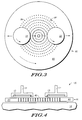
- FIG. 3 includes an illustration of a polishing pad 81 having a plurality of openings in accordance with one embodiment of the present invention.
- Polishing pad 81 has a first region 83 and a second region 82.
- the thickness of the polishing pad 81 is substantially uniform across its surface.
- the second region 82 has a plurality of openings 84.
- Each opening 84 has a width that is in a range of 1) about 250-1000 microns or 2) about 25-1000 percent larger than the average pore size.
- the openings 84 occupy in a range of about 5-50 percent of the polishing surface area within region 82.
- region 82 may have a plurality of openings 84 that are each about 500 microns, and the total surface area of region 82 that is occupied by the openings 84 may be about 30 percent.
- the rotational and oscillating directions of motion of the polishing pad 81 and the substrates 13 are shown in FIG. 3.
- the openings 84 within the second region 82 help to increase the polishing rate within the second region 82 compared to a conventional polishing pad that does not have any openings.
- the edge of the substrate is exposed to the openings 84 only a portion of the time, while the center of the substrate 13 is virtually always overlying the second region 82 that includes the openings 84.
- the higher relative velocity between the substrate 13 and the pad 81 causes an increased polishing rate, while a shorter, if any, exposure time to the openings 84 causes a decreased polishing rate.
- the lower relative velocity between the substrate 13 and the pad 81 causes a decreased polishing rate, while the longer exposure time to the openings 84 causes an increased polishing rate. In this manner the polishing rate of the substrate 13 may be made more uniform across the primary surface of the substrate 13 compared to the prior art polishing pad 11.
- FIG. 4 includes a cross-sectional view of the polisher 10 with the polishing pad 81.
- the polishing pad 81 is attached to the platen 14 with an adhesive compound (not shown).
- the substrates 13 are held by the substrate holders 12.
- the center point of the substrate should always be over the region 82 of the polishing pad 81. If the region 82 is too large, the polishing rate across the substrate may not be uniform enough. On average, about 20-80 percent of the primary surface of each substrate is in contact with region 82 during polishing. Therefore, region 82 extends a distance of about 50-80 percent from the center of the polishing pad to the edge of the polishing pad.
- the openings 84 are shown extending through the polishing pad 81. The openings 84 help the polishing slurry to move through the polishing pad 81.
- FIG. 5 illustrates another embodiment of the present invention.
- a polishing pad 101 has a three regions including a first region 104, a second region 102, and a third region 103.
- the second region 102 has a band of openings 84 that are similar in shape and in density to the openings 84 within the second region 82 of the polishing pad 81.
- FIG. 5 illustrates the first region 104 and the third region 103 to have no openings 84, either or both may have openings.
- the width of the openings within the region 104 should not be any wider than the width of openings within region 103, or the density of openings within the region 104 should not be any higher than the density of openings within region 103.
- the width of the openings within the region 103 should not be any wider than the width of openings 84 within region 102, or the density of openings within the region 103 should not be any higher than the density of openings 84 within region 102.
- FIG. 6 illustrates a cross-sectional view of polishing pad 101 and substrates 13.
- the width of the second region 102 is about 20-80 percent of a dimension of the primary surface of the substrate 13. If substrate 13 would be a wafer about 200 millimeters in diameter, then the primary surface dimension would be about 200 millimeters. If the width of the second region 102 would be about 50 percent of the primary surface dimension of the wafer, the width of the second region 102 would be about 100 millimeters wide. This example is to illustrate and not to limit the invention.
- FIG. 7 includes an illustration of another embodiment of the present invention.
- FIG. 7 includes a polishing pad 71 that is similar to the polishing pad 101 of FIGs. 5 and 6.
- Polishing pad 71 includes a first region 74, a second region 72, and a third region 73.
- the openings 75 extend only partially through the polishing pad 74.
- the depth of the openings 75 should be as least as large as the difference in topography along the surface of the substrates 13. For example, if the difference in topography along the surface of one of the substrates 13 is about two microns, the depth of the openings 84 should be at least about two microns.
- the openings 75 must extend at least about two microns down from the surface of the polishing pad 71. In FIG. 7, the openings 75 extend about half way through the polishing pad 71. The openings 75 are about 0.5- 1.0 millimeters deep depending on the thickness of the polishing pad 74.
- the manufacturing of the polishing pads is not expected to be difficult and may be performed in different manners.
- the openings 75 or 84 may be formed by laser ablation, or possibly machining the polishing pad by drilling. Laser ablation is used in scribing identification marks onto silicon substrates, and a YAG or excimer laser may be used in the laser ablation. The manner for forming the openings by laser ablation would be similar to the method used for scribing wafers. Drilling the openings 75 or 84 may be performed, but the drilling machine needs to be able to form the small widths of the openings and have good precision so that the opening density may be controlled. Currently, computer-controlled machine tools are expected to be capable of forming the openings by drilling.
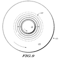
- a polishing pad 121 is formed with average pore sizes that vary across the surface of the polishing pad.
- Region 122 has pores with an average pore size that decreases with the distance from the center of the polishing pad 121.
- Region 123 has an average pore size that is roughly equivalent to the average pore size of a conventional polishing pad. Therefore, region 123 has an average pore size of about 100-200 microns wide, while region 122 has an average pore size that is in a range of 1) about 250-1000 microns or 2) about 25-1000 percent larger than the average pore size of region 123.
- the larger average pore size may be formed by locally heating a portion of the polishing pad while the reaction to form the polishing pad occurs.
- a heat probe is placed within the reacting cylinder used to form a cylindrical block of polyurethane.
- the heat probe would traverse the cylinder along its radial centerline, and the probe would be on while the chemicals react to form polyurethane.
- the locally higher temperature near the center of the cylinder should cause larger pores to form near the center of the cylinder compared to the edge of the cylinder.
- electromagnetic radiation such as microwaves and the like, may be focused such that the radiation causes local heating where larger pores are to be formed. If the radiation is focused and the cylinder is rotated during the polyurethane reaction, a band of larger pores may be formed at a location similar to the openings 84 of the polishing pad 101 of FIGs. 5 and 6.
- the polishing pads of the present invention may be used in virtually any application of chemical-mechanical polishing of semiconductor substrates. No special equipment modifications should be required. Many of the operating parameters when using any one of the polishing pads should be similar to the operating parameters using a conventional polishing pad. Any one of the polishing pad as illustrated in FIGs. 3-9 is attached to the platen 14 of the polisher 10 similar to a conventional polishing pad. The substrate holders 12 and the substrates 13 do not need to be treated or modified. The slurry composition, platen rotational velocity, and substrate rotational velocity are all expected to be within the normal operating parameters of a polisher that would have a conventional polishing pad. The oscillating range may be more that what is typically used in the prior art. Slight adjustment to other operating parameters may be needed to optimize polishing performance.
- the oscillating motion includes an oscillating range and an oscillating velocity.
- the oscillating range depends on a dimension of the primary surface of the substrate to be polished and a dimension of the second region of the polishing pad and the size of the semiconductor substrate.
- a semiconductor substrate oscillates in either direction no more than about 40 percent of the dimension of the primary surface.
- the oscillating range is typically a distance that is no more than 80 percent of a dimension of the primary surface of the semiconductor substrate.
- a limitation on the oscillating range is that the center point of the semiconductor substrate should always overlie the second region of the polishing pad during the polishing step.
- Another limitation on the oscillating range is that the edge of the semiconductor substrate should not extend beyond the edge of the polishing pad during polishing.
- the semiconductor substrate should be moved so that the outermost point of the semiconductor substrate lines up with the outermost point of the second region of the polishing pad some time during the polishing step.
- the reference point for "outermost" is the center of the polishing pad. Therefore, the outermost point of the semiconductor substrate is that point which is furthest from the center of the polishing pad, and the outermost point of the second region is that point which is furthest from the center of the polishing pad.
- the oscillating range is a distance that is in a range of 5-50 percent of the dimension of the primary surface of the semiconductor substrate.
- the semiconductor substrate is a wafer having a diameter of about 150 millimeters and that the polishing pad of FIGs. 5 and 6 is used.
- the width of the region 102 is about 33 percent of the diameter of the wafer or about 50 millimeters.
- the semiconductor substrate extends about 50 millimeters beyond each edge of the region 102. Therefore, the semiconductor substrates 13 oscillate about 25 millimeters to the right and about 25 millimeters to the left.
- the oscillating range is about 50 millimeters. If the oscillating range in this case is reduced, the outermost point of the wafer does not line up the outermost point of the region 102. If the oscillating range in this case is increased, the center point of the wafer does not overlie the region 102 during at least some portion of the polishing step.
- the width of region 102 is about 80 percent of the diameter of the wafer or about 120 millimeters.
- the semiconductor substrates 13 are oscillated at least about 15 millimeters in each direction, so that the outermost point of the wafer line up with the outermost portion of region 102 during the polishing step.
- the oscillating range is at least about 30 millimeters.
- the semiconductor substrates 13 are oscillated no more than about 60 millimeters in each direction, so that the center point of the wafer always overlies region 102 during the polishing step.
- the oscillating range is no more than about 120 millimeters.
- the semiconductor substrates 13 are oscillated in a range of about 15-60 millimeters in each direction.
- the oscillating range is about 30-120 millimeters.
- the oscillating velocity is in a range of about 1-10 millimeters per second for either of the cases described.
- the present invention includes many benefits.
- the polishing pads of the present invention may be used in many commercial chemical-mechanical polishers without any significant changes to the equipment.
- the polishing parameters other than lateral back and forth motion are not expected to be significantly changed. Although the lateral motion may change, little or no adjustment to the other processing parameters may be necessary in order to achieve optimal polishing of the semiconductor substrate.
- the polishing pads of the present invention are expected to have more uniform polishing characteristics. Many of the prior art polishing pads have geometric patterns that are suppose to increase polishing rate and uniformity. In particular, one prior art polishing pad has an opening density that is higher toward the edge of the polishing pad. Contrary to the beliefs of the prior art, I believe that pad with is higher opening density near the edge that is expected to contribute to further polishing nonuniformity. It should be kept in mind that the platen and semiconductor substrates typically rotate in the same direction. Therefore, the relative velocity of the semiconductor substrate to the polishing pad is the highest at the edge of the semiconductor substrate when it is the closest to the edge of the polishing pad.
- the present invention helps to increase the polishing rate at the center of the substrate more than it helps to increase the polishing rate near the edge of the substrate.
- the polishing rate is more uniform across the primary surface of the substrate because slurry transport and polishing product removal from the second regions 72, 82, or 102 is enhanced.
- the openings or larger average pore size help to decrease the likelihood that the pores 74 or the pores adjacent to the openings 84 within the second region 72, 82, or 102 become clogged compared to a conventional pad. If the pores become clogged, the polishing rate at the location where the pore is located generally decreases. Therefore, polishing pads of the present invention are expected to have a more uniform polishing rate because the pores adjacent to the pores 74 and openings 84 are less likely to become clogged.
- the polishing pads of the present invention are expected to last longer because the pores are less likely to become clogged. After the pores become clogged, a polishing pad may need to be replaced or "reconditioned.” Reconditioning is performed with an abrading tool, such as a diamond disk and the like. The reconditioning is typically a destructive process because pores in the polishing pad material near the surface of the polishing pad are almost always ripped open during reconditioning. Reconditioning usually reduces the lifetime of the polishing pad because reconditioning is a destructive operation. The present invention should extend the lifetime of a polishing pad because the larger pores or openings reduce the likelihood of pores becoming clogged. The present invention is not expected to require reconditioning.
- the pores 74 or openings 84 are on the order of hundreds of microns. If the pores or openings are too large, such as on the order of centimeters, a center of the substrate would spend a large time over these very large openings.
- the local polishing rate of a point on the substrate is low or close to zero when the point is over an opening compared to a point that does not lie over an opening. When the openings are too large, part of the substrate is spending too much time over an opening, which should decrease the polishing rate.
- each opening can only reduced pore clogging over a limited area immediately adjacent to the opening.
- the polishing pad may have points on the polishing pad that are far enough away from the very large openings where pore clogging may still occur.
- the density of these pores or openings may be adjusted to help reduce the likelihood of pore clogging.
- the polishing pads of the present invention may not need to be conditioned prior to using them.
- the conditioning may include rubbing with an abrading tool or processing dummy wafers.
- the abrading tool is actually destructive to the polishing pad.
- a polishing pad can generally process a finite number of substrates before the polishing pad needs to be replaced. If dummy wafers are processed, the number of substrates that can be processed on that same polishing pad may be less than if dummy wafers were not processed. By not conditioning the pad, the polishing pad may process a larger number of substrates.
- the present invention is not limited by the embodiments or materials listed herein.
- the polishing pads of the present invention may be used on a polisher capable of polishing any number of semiconductor substrates during the same polishing step.
Abstract
Description
- The present invention relates to the field of semiconductor devices, and in particular, to polishing pads used in chemical-mechanical polishing semiconductor substrates.
- Planarization of semiconductor substrates is becoming more important as the number of layers used to form a semiconductor device increases. Nonplanar semiconductor substrates have many problems including difficulty in patterning a photoresist layer, formation of a void within a film during the film deposition, and incomplete removal of a layer during an etch process leaving residual portions of the layer, which are sometimes called "stringers." A number of planarization processes have been developed and include chemical-mechanical polishing.
- FIG. 1 and 2 include illustrations of a part of one type of a chemical-mechanical polisher that is used to polish semiconductor substrates. FIG. 1 is a cross-sectional view of a chemical-
mechanical polisher 10. Thepolisher 10 has aplaten 14 and apolishing pad 11 attached to theplaten 14 with an adhesive compound (not shown). Above thepolishing pad 11 aresubstrate holders 12, and eachsubstrate holder 12 has asemiconductor substrate 13. Thepolisher 10 also includes a polishing slurry and a slurry feed, both of which are not shown. Thepolishing pad 11 may be made of a porous polyurethane material that has a relatively uniform thickness of about 1-2 millimeters. FIG. 2 includes a top view illustrating the relationships of motion between thepolishing pad 11 and thesubstrates 13. During polishing, thepolishing pad 11 rotates counterclockwise or clockwise, but thesubstrates 13 typically rotate in the same direction as thepolishing pad 11. While thesubstrates 13 andpolishing pad 11 are rotating, thesubstrates 13 are being oscillated back and forth across the polishing pad. The oscillating motion covers a distance called an oscillating range and is performed at an oscillating velocity. While the polishing is being performed, the polishing slurry may be recycled. - In actual use, chemical-mechanical polishing typically has nonuniform polishing rates across a substrate surface. In many cases, the polishing rate near the edge of the substrate is higher than the polishing rate near the center of the substrate because the relative velocity between polishing pad and the substrate is higher near the edge of the substrate compared to the center of the substrate. Therefore, some area of the substrate near the center may be underpolished, some area of the substrate near the edge may be overpolished, or both.
- The polishing pad may contribute to the nonuniformity. A brief overview of the formation of polyurethane polishing pads is now presented. Polyurethane polishing pads are typically formed by reacting the chemicals that form polyurethane within a cylindrical container. After forming a cylindrical-shaped piece of polyurethane, the piece is cut into slices that are subsequently used as polishing pad. The polishing pad typically has pores that have a size of about 100-200 microns. Although the pores may vary in size, the average pore size for any region of the polishing pad is typically about the same as any other region of the polishing pad. As used hereinafter, this type of prior art polishing pad is referred to as a conventional polishing pad. The nonuniformity occurs because the edge of the substrate is moving faster relative to the polishing pad compared to the center of the substrate and the conventional polishing pad does not have a feature to compensate of the polishing nonuniformity.
- The prior art has addressed the problem of nonuniform polishing by modifying a conventional polishing pad by forming a pattern within the polishing pad. These polishing pads include forming a variety of geometric patterns including openings. It should be kept in mind that polishing pads are typically porous, and the pores are formed during the reaction to form the polishing pad material. As used in this specification, openings are distinguished from pores because openings are formed within the pad after the reaction to form the polishing pad material has occurred. A conventional polishing pad has pores but does not have any openings. The prior art polishing pad with openings typically have a width on the order of centimeters, or the prior art polishing pad has a density of openings that decreases with the distance from edge of the polishing pad.
- The present invention includes a polishing pad to improve polishing uniformity across a substrate and a method using the polishing pad. The polishing pad has a first region adjacent to the edge of the polishing pad and a second region that is adjacent to the first region and further from the edge of the polishing pad. The polishing pad is configured such that second region has a plurality of openings or has an average pore size that is larger than the average pore size of the first region. The present invention also includes openings within the first region, wherein the width or density of openings within the first region is smaller than the width or density of openings within the second region. The polishing pad may be used in a chemical-mechanical polishing without having to substantially change the equipment or the operational parameters of the polisher other than oscillating range.
- Other features and advantages of the present invention will be apparent from the accompanying drawings and from the detailed description that follows.
- The present invention is illustrated by way of example and not limitation in the figures of the accompanying drawings, in which like references indicate similar elements, and in which:
- FIGs. 1 and 2 include cross-sectional and top views of a polishing pad and substrates. (Prior art)
- FIGs. 3-4 include cross-sectional and top views of a polishing pad and substrates, wherein the polishing pad has a plurality of openings in accordance with one embodiment of the present invention.
- FIGs. 5-6 include cross-sectional and top views of a polishing pad and substrates, wherein the polishing pad has a plurality of openings in accordance with another embodiment of the present invention.
- FIG. 7 includes a cross-sectional view of a polishing pad and substrates, wherein the polishing pad has a plurality of openings in accordance with another embodiment of the present invention.
- FIGs. 8-9 include cross-sectional and top views of a polishing pad and substrates, wherein the polishing pad has a region with larger average pore size in accordance with another embodiment of the present invention.
- The present invention includes a polishing pad to improve polishing uniformity across a substrate and a method using the polishing pad. The polishing pad has a first region adjacent to the edge of the polishing pad and a second region that is adjacent to the first region and further from the edge compared to the first region. As is discussed in more detail below, the second region has a plurality of openings or a larger average pore size compared to the first region. Equipment modifications and polishing parameters are not substantially affected when using a polishing pad of the present invention except for oscillating range.
- All of the polishing pads in FIGs. 3-7 include of a porous polyurethane material that has an average pore size of about 100-200 microns. FIG. 3 includes an illustration of a
polishing pad 81 having a plurality of openings in accordance with one embodiment of the present invention.Polishing pad 81 has afirst region 83 and asecond region 82. The thickness of thepolishing pad 81 is substantially uniform across its surface. Thesecond region 82 has a plurality ofopenings 84. Eachopening 84 has a width that is in a range of 1) about 250-1000 microns or 2) about 25-1000 percent larger than the average pore size. Cumulatively, theopenings 84 occupy in a range of about 5-50 percent of the polishing surface area withinregion 82. For example,region 82 may have a plurality ofopenings 84 that are each about 500 microns, and the total surface area ofregion 82 that is occupied by theopenings 84 may be about 30 percent. The rotational and oscillating directions of motion of thepolishing pad 81 and thesubstrates 13 are shown in FIG. 3. Theopenings 84 within thesecond region 82 help to increase the polishing rate within thesecond region 82 compared to a conventional polishing pad that does not have any openings. Because thesubstrate 13 is rotating during the polishing, the edge of the substrate is exposed to theopenings 84 only a portion of the time, while the center of thesubstrate 13 is virtually always overlying thesecond region 82 that includes theopenings 84. At thefirst region 83, the higher relative velocity between thesubstrate 13 and thepad 81 causes an increased polishing rate, while a shorter, if any, exposure time to theopenings 84 causes a decreased polishing rate. In thesecond region 82, the lower relative velocity between thesubstrate 13 and thepad 81 causes a decreased polishing rate, while the longer exposure time to theopenings 84 causes an increased polishing rate. In this manner the polishing rate of thesubstrate 13 may be made more uniform across the primary surface of thesubstrate 13 compared to the priorart polishing pad 11. - FIG. 4 includes a cross-sectional view of the
polisher 10 with thepolishing pad 81. Thepolishing pad 81 is attached to theplaten 14 with an adhesive compound (not shown). Thesubstrates 13 are held by thesubstrate holders 12. The center point of the substrate should always be over theregion 82 of thepolishing pad 81. If theregion 82 is too large, the polishing rate across the substrate may not be uniform enough. On average, about 20-80 percent of the primary surface of each substrate is in contact withregion 82 during polishing. Therefore,region 82 extends a distance of about 50-80 percent from the center of the polishing pad to the edge of the polishing pad. Theopenings 84 are shown extending through thepolishing pad 81. Theopenings 84 help the polishing slurry to move through thepolishing pad 81. - FIG. 5 illustrates another embodiment of the present invention. A
polishing pad 101 has a three regions including afirst region 104, asecond region 102, and athird region 103. Thesecond region 102 has a band ofopenings 84 that are similar in shape and in density to theopenings 84 within thesecond region 82 of thepolishing pad 81. Although FIG. 5 illustrates thefirst region 104 and thethird region 103 to have noopenings 84, either or both may have openings. The width of the openings within theregion 104 should not be any wider than the width of openings withinregion 103, or the density of openings within theregion 104 should not be any higher than the density of openings withinregion 103. The width of the openings within theregion 103 should not be any wider than the width ofopenings 84 withinregion 102, or the density of openings within theregion 103 should not be any higher than the density ofopenings 84 withinregion 102. - FIG. 6 illustrates a cross-sectional view of
polishing pad 101 andsubstrates 13. The width of thesecond region 102 is about 20-80 percent of a dimension of the primary surface of thesubstrate 13. Ifsubstrate 13 would be a wafer about 200 millimeters in diameter, then the primary surface dimension would be about 200 millimeters. If the width of thesecond region 102 would be about 50 percent of the primary surface dimension of the wafer, the width of thesecond region 102 would be about 100 millimeters wide. This example is to illustrate and not to limit the invention. - FIG. 7 includes an illustration of another embodiment of the present invention. FIG. 7 includes a
polishing pad 71 that is similar to thepolishing pad 101 of FIGs. 5 and 6.Polishing pad 71 includes afirst region 74, asecond region 72, and athird region 73. Unlike FIGs. 5 and 6, theopenings 75 extend only partially through thepolishing pad 74. In general, the depth of theopenings 75 should be as least as large as the difference in topography along the surface of thesubstrates 13. For example, if the difference in topography along the surface of one of thesubstrates 13 is about two microns, the depth of theopenings 84 should be at least about two microns. In other words, theopenings 75 must extend at least about two microns down from the surface of thepolishing pad 71. In FIG. 7, theopenings 75 extend about half way through thepolishing pad 71. Theopenings 75 are about 0.5- 1.0 millimeters deep depending on the thickness of thepolishing pad 74. - The manufacturing of the polishing pads is not expected to be difficult and may be performed in different manners. The
openings openings - In an embodiment shown in FIG. 8, a
polishing pad 121 is formed with average pore sizes that vary across the surface of the polishing pad.Region 122 has pores with an average pore size that decreases with the distance from the center of thepolishing pad 121.Region 123 has an average pore size that is roughly equivalent to the average pore size of a conventional polishing pad. Therefore,region 123 has an average pore size of about 100-200 microns wide, whileregion 122 has an average pore size that is in a range of 1) about 250-1000 microns or 2) about 25-1000 percent larger than the average pore size ofregion 123. The larger average pore size may be formed by locally heating a portion of the polishing pad while the reaction to form the polishing pad occurs. In one method to form the polishing pad, a heat probe is placed within the reacting cylinder used to form a cylindrical block of polyurethane. The heat probe would traverse the cylinder along its radial centerline, and the probe would be on while the chemicals react to form polyurethane. The locally higher temperature near the center of the cylinder should cause larger pores to form near the center of the cylinder compared to the edge of the cylinder. In still another embodiment, electromagnetic radiation, such as microwaves and the like, may be focused such that the radiation causes local heating where larger pores are to be formed. If the radiation is focused and the cylinder is rotated during the polyurethane reaction, a band of larger pores may be formed at a location similar to theopenings 84 of thepolishing pad 101 of FIGs. 5 and 6. Neither process is destructive meaning that the polyurethane polishing pad has virtually the same characteristics of a conventional polishing pad except that the pore size varies. The methods listed above for forming the polyurethane pad are illustrative and are not to be considered limiting. - The polishing pads of the present invention may be used in virtually any application of chemical-mechanical polishing of semiconductor substrates. No special equipment modifications should be required. Many of the operating parameters when using any one of the polishing pads should be similar to the operating parameters using a conventional polishing pad. Any one of the polishing pad as illustrated in FIGs. 3-9 is attached to the
platen 14 of thepolisher 10 similar to a conventional polishing pad. Thesubstrate holders 12 and thesubstrates 13 do not need to be treated or modified. The slurry composition, platen rotational velocity, and substrate rotational velocity are all expected to be within the normal operating parameters of a polisher that would have a conventional polishing pad. The oscillating range may be more that what is typically used in the prior art. Slight adjustment to other operating parameters may be needed to optimize polishing performance. - The oscillating motion includes an oscillating range and an oscillating velocity. The oscillating range depends on a dimension of the primary surface of the substrate to be polished and a dimension of the second region of the polishing pad and the size of the semiconductor substrate. Typically, a semiconductor substrate oscillates in either direction no more than about 40 percent of the dimension of the primary surface. The oscillating range is typically a distance that is no more than 80 percent of a dimension of the primary surface of the semiconductor substrate. A limitation on the oscillating range is that the center point of the semiconductor substrate should always overlie the second region of the polishing pad during the polishing step. Another limitation on the oscillating range is that the edge of the semiconductor substrate should not extend beyond the edge of the polishing pad during polishing. The semiconductor substrate should be moved so that the outermost point of the semiconductor substrate lines up with the outermost point of the second region of the polishing pad some time during the polishing step. The reference point for "outermost" is the center of the polishing pad. Therefore, the outermost point of the semiconductor substrate is that point which is furthest from the center of the polishing pad, and the outermost point of the second region is that point which is furthest from the center of the polishing pad. In most applications, the oscillating range is a distance that is in a range of 5-50 percent of the dimension of the primary surface of the semiconductor substrate.
- For example, assume that the semiconductor substrate is a wafer having a diameter of about 150 millimeters and that the polishing pad of FIGs. 5 and 6 is used. In a first case, assume that the width of the
region 102 is about 33 percent of the diameter of the wafer or about 50 millimeters. When wafer would be centered overregion 102 similar to FIG. 6, the semiconductor substrate extends about 50 millimeters beyond each edge of theregion 102. Therefore, thesemiconductor substrates 13 oscillate about 25 millimeters to the right and about 25 millimeters to the left. The oscillating range is about 50 millimeters. If the oscillating range in this case is reduced, the outermost point of the wafer does not line up the outermost point of theregion 102. If the oscillating range in this case is increased, the center point of the wafer does not overlie theregion 102 during at least some portion of the polishing step. - In a second case, assume that the width of
region 102 is about 80 percent of the diameter of the wafer or about 120 millimeters. The semiconductor substrates 13 are oscillated at least about 15 millimeters in each direction, so that the outermost point of the wafer line up with the outermost portion ofregion 102 during the polishing step. The oscillating range is at least about 30 millimeters. The semiconductor substrates 13 are oscillated no more than about 60 millimeters in each direction, so that the center point of the wafer always overliesregion 102 during the polishing step. The oscillating range is no more than about 120 millimeters. In this case, thesemiconductor substrates 13 are oscillated in a range of about 15-60 millimeters in each direction. The oscillating range is about 30-120 millimeters. The oscillating velocity is in a range of about 1-10 millimeters per second for either of the cases described. - The present invention includes many benefits. The polishing pads of the present invention may be used in many commercial chemical-mechanical polishers without any significant changes to the equipment. The polishing parameters other than lateral back and forth motion are not expected to be significantly changed. Although the lateral motion may change, little or no adjustment to the other processing parameters may be necessary in order to achieve optimal polishing of the semiconductor substrate.
- The polishing pads of the present invention are expected to have more uniform polishing characteristics. Many of the prior art polishing pads have geometric patterns that are suppose to increase polishing rate and uniformity. In particular, one prior art polishing pad has an opening density that is higher toward the edge of the polishing pad. Contrary to the beliefs of the prior art, I believe that pad with is higher opening density near the edge that is expected to contribute to further polishing nonuniformity. It should be kept in mind that the platen and semiconductor substrates typically rotate in the same direction. Therefore, the relative velocity of the semiconductor substrate to the polishing pad is the highest at the edge of the semiconductor substrate when it is the closest to the edge of the polishing pad. Unlike the prior art, the present invention helps to increase the polishing rate at the center of the substrate more than it helps to increase the polishing rate near the edge of the substrate. The polishing rate is more uniform across the primary surface of the substrate because slurry transport and polishing product removal from the
second regions - The openings or larger average pore size help to decrease the likelihood that the
pores 74 or the pores adjacent to theopenings 84 within thesecond region pores 74 andopenings 84 are less likely to become clogged. - The polishing pads of the present invention are expected to last longer because the pores are less likely to become clogged. After the pores become clogged, a polishing pad may need to be replaced or "reconditioned." Reconditioning is performed with an abrading tool, such as a diamond disk and the like. The reconditioning is typically a destructive process because pores in the polishing pad material near the surface of the polishing pad are almost always ripped open during reconditioning. Reconditioning usually reduces the lifetime of the polishing pad because reconditioning is a destructive operation. The present invention should extend the lifetime of a polishing pad because the larger pores or openings reduce the likelihood of pores becoming clogged. The present invention is not expected to require reconditioning.
- The
pores 74 oropenings 84 are on the order of hundreds of microns. If the pores or openings are too large, such as on the order of centimeters, a center of the substrate would spend a large time over these very large openings. In general, the local polishing rate of a point on the substrate is low or close to zero when the point is over an opening compared to a point that does not lie over an opening. When the openings are too large, part of the substrate is spending too much time over an opening, which should decrease the polishing rate. In addition, each opening can only reduced pore clogging over a limited area immediately adjacent to the opening. When very large openings are used, the polishing pad may have points on the polishing pad that are far enough away from the very large openings where pore clogging may still occur. By keeping the size of the pores or openings on the order of hundreds of microns, the density of these pores or openings may be adjusted to help reduce the likelihood of pore clogging. - The polishing pads of the present invention may not need to be conditioned prior to using them. The conditioning may include rubbing with an abrading tool or processing dummy wafers. The abrading tool is actually destructive to the polishing pad. A polishing pad can generally process a finite number of substrates before the polishing pad needs to be replaced. If dummy wafers are processed, the number of substrates that can be processed on that same polishing pad may be less than if dummy wafers were not processed. By not conditioning the pad, the polishing pad may process a larger number of substrates.
- The present invention is not limited by the embodiments or materials listed herein. The polishing pads of the present invention may be used on a polisher capable of polishing any number of semiconductor substrates during the same polishing step.
- In the foregoing specification, the invention has been described with reference to specific embodiments thereof. It will, however, be evident that various modifications and changes made thereto without departing from the broader spirit or scope of the invention as set forth in the appended claims. The specification and drawings are, accordingly, to be regarded in an illustrative rather than a restrictive sense.
Claims (8)
- A polishing pad (81, 101, 71, 121) for polishing a semiconductor substrate (13), wherein the polishing pad comprises:
an edge;
a first region (83, 104, 74, 123) including a plurality of pores having a first average pore size, wherein the first region lies adjacent to the edge; and
a second region (82, 102, 72, 122) including a plurality of pores having a second average pore size, wherein the second region (82, 102, 72, 122) lies adjacent to the first region and further from the edge compared to the first region (83, 104, 74, 123),
wherein the polishing pad (81, 101, 71, 121) is
characterized by:
the second region (82, 102, 72) having a plurality of openings (84, 75), wherein each opening of the plurality of openings (84, 75):
has a width of about 250-1000 microns; or
has a width that is in a range of about 25-1000 percent larger than the average pore size of the first region; or
the second average pore size being larger than the first average pore size. - The polishing pad (81, 101, 71) of claim 1, further
characterized in that:
the polishing pad (81, 101, 71) has a polishing surface area; and
the plurality of openings occupies about 5-50 percent of the polishing surface area within the second region (82, 102, 72). - The polishing pad of claim 1, further characterized in that:
the first region includes a plurality of openings and a first opening density;
the second region has a second opening density; and
the second opening density is higher than the first opening density. - The polishing pad of claim 1, further characterized in that:
the first region includes a plurality of openings having a first average opening width;
the plurality of openings of the second region has a second average opening width; and
the second average opening width is wider than the first average opening width. - The polishing pad of claim 1, further characterized by a third region, wherein:
the third region is adjacent to the second region;
the third region is furthest from the edge compared to the first and second regions;
the third region includes a plurality of openings having a third average opening width and a third opening density;
the second region has a second opening density; and
the polishing pad has a configuration selected from a group consisting of:
the second opening density is no less than the third opening density; and
the second average opening width is no less than the third average opening width. - A method of polishing a semiconductor substrate (13) having a center point and a primary surface having a primary surface dimension, wherein the method comprises the steps of:
placing the substrate (13) in a polisher (10); and
polishing the substrate (13) with a polishing pad (81, 101, 71, 121), wherein the polishing pad (81, 101, 71, 121) includes:
an edge;
a first region (83, 104, 74, 123) including a plurality of pores having a first average pore size, wherein the first region lies adjacent to the edge; and
a second region (82, 102, 72, 122) including a plurality of pores having a second average pore size, wherein the second legion (82, 102, 72, 122) lies adjacent to the first region (83, 104, 74, 123) and further from the edge compared to the first region (83, 104, 74, 123),
wherein the polishing pad (81, 101, 71, 121) is
characterized by:
the second region (82, 102, 72) having a plurality of openings (84, 75), wherein each opening of the plurality of openings (84, 75):
has a width of about 250-1000 microns; or
has a width that is in a range of about 25-1000 percent larger than the average pore size of the first region; or
the second average pore size being larger than the first average pore size. - The method of claim 6, further characterized by the polishing step is performed such that the center point of the substrate (13) is always over the second region (82, 102, 72, 122) during the polishing step.
- The method of claim 6, further characterized by the polishing step includes oscillating the semiconductor substrate (13) across a portion of the polishing pad (81, 101, 71, 121), wherein the oscillating:
covers an oscillating range that is a distance in a range of about 5-50 percent of the primary surface dimension; and
is performed at an oscillating velocity that is in a range of about 1-10 millimeters per second.
Applications Claiming Priority (2)
| Application Number | Priority Date | Filing Date | Title |
|---|---|---|---|
| US54168 | 1993-04-30 | ||
| US08/054,168 US5329734A (en) | 1993-04-30 | 1993-04-30 | Polishing pads used to chemical-mechanical polish a semiconductor substrate |
Publications (2)
| Publication Number | Publication Date |
|---|---|
| EP0622155A1 true EP0622155A1 (en) | 1994-11-02 |
| EP0622155B1 EP0622155B1 (en) | 1997-10-08 |
Family
ID=21989192
Family Applications (1)
| Application Number | Title | Priority Date | Filing Date |
|---|---|---|---|
| EP94104688A Expired - Lifetime EP0622155B1 (en) | 1993-04-30 | 1994-03-24 | Polishing pad and a method of polishing a semiconductor substrate |
Country Status (5)
| Country | Link |
|---|---|
| US (1) | US5329734A (en) |
| EP (1) | EP0622155B1 (en) |
| JP (1) | JP3425216B2 (en) |
| DE (1) | DE69406041T2 (en) |
| TW (1) | TW228606B (en) |
Cited By (1)
| Publication number | Priority date | Publication date | Assignee | Title |
|---|---|---|---|---|
| EP1430520A1 (en) * | 2001-08-02 | 2004-06-23 | SKC Co., Ltd. | Chemical mechanical polishing pad with micro-holes |
Families Citing this family (91)
| Publication number | Priority date | Publication date | Assignee | Title |
|---|---|---|---|---|
| USRE37997E1 (en) * | 1990-01-22 | 2003-02-18 | Micron Technology, Inc. | Polishing pad with controlled abrasion rate |
| MY114512A (en) * | 1992-08-19 | 2002-11-30 | Rodel Inc | Polymeric substrate with polymeric microelements |
| US7037403B1 (en) * | 1992-12-28 | 2006-05-02 | Applied Materials Inc. | In-situ real-time monitoring technique and apparatus for detection of thin films during chemical/mechanical polishing planarization |
| US6614529B1 (en) * | 1992-12-28 | 2003-09-02 | Applied Materials, Inc. | In-situ real-time monitoring technique and apparatus for endpoint detection of thin films during chemical/mechanical polishing planarization |
| JP2622069B2 (en) * | 1993-06-30 | 1997-06-18 | 三菱マテリアル株式会社 | Dressing equipment for polishing cloth |
| US5938504A (en) * | 1993-11-16 | 1999-08-17 | Applied Materials, Inc. | Substrate polishing apparatus |
| US5441598A (en) * | 1993-12-16 | 1995-08-15 | Motorola, Inc. | Polishing pad for chemical-mechanical polishing of a semiconductor substrate |
| US5536202A (en) * | 1994-07-27 | 1996-07-16 | Texas Instruments Incorporated | Semiconductor substrate conditioning head having a plurality of geometries formed in a surface thereof for pad conditioning during chemical-mechanical polish |
| ES2137459T3 (en) * | 1994-08-09 | 1999-12-16 | Ontrak Systems Inc | LINEAR POLISHING AND METHOD FOR PLANNING SEMICONDUCTIVE PILLS. |
| US5571044A (en) * | 1994-10-11 | 1996-11-05 | Ontrak Systems, Inc. | Wafer holder for semiconductor wafer polishing machine |
| US5593344A (en) * | 1994-10-11 | 1997-01-14 | Ontrak Systems, Inc. | Wafer polishing machine with fluid bearings and drive systems |
| US5575707A (en) * | 1994-10-11 | 1996-11-19 | Ontrak Systems, Inc. | Polishing pad cluster for polishing a semiconductor wafer |
| US5609719A (en) * | 1994-11-03 | 1997-03-11 | Texas Instruments Incorporated | Method for performing chemical mechanical polish (CMP) of a wafer |
| US5893796A (en) * | 1995-03-28 | 1999-04-13 | Applied Materials, Inc. | Forming a transparent window in a polishing pad for a chemical mechanical polishing apparatus |
| DE69635816T2 (en) | 1995-03-28 | 2006-10-12 | Applied Materials, Inc., Santa Clara | Method for producing an apparatus for in situ control and determination of the end of chemical mechanical grading operations |
| US6876454B1 (en) | 1995-03-28 | 2005-04-05 | Applied Materials, Inc. | Apparatus and method for in-situ endpoint detection for chemical mechanical polishing operations |
| US5533923A (en) * | 1995-04-10 | 1996-07-09 | Applied Materials, Inc. | Chemical-mechanical polishing pad providing polishing unformity |
| US5945347A (en) | 1995-06-02 | 1999-08-31 | Micron Technology, Inc. | Apparatus and method for polishing a semiconductor wafer in an overhanging position |
| US5868605A (en) * | 1995-06-02 | 1999-02-09 | Speedfam Corporation | In-situ polishing pad flatness control |
| US5632667A (en) * | 1995-06-29 | 1997-05-27 | Delco Electronics Corporation | No coat backside wafer grinding process |
| US5897424A (en) * | 1995-07-10 | 1999-04-27 | The United States Of America As Represented By The Secretary Of Commerce | Renewable polishing lap |
| US5658185A (en) * | 1995-10-25 | 1997-08-19 | International Business Machines Corporation | Chemical-mechanical polishing apparatus with slurry removal system and method |
| US5609517A (en) * | 1995-11-20 | 1997-03-11 | International Business Machines Corporation | Composite polishing pad |
| DE69717510T2 (en) * | 1996-01-24 | 2003-10-02 | Lam Res Corp | Wafer polishing head |
| US5916012A (en) * | 1996-04-26 | 1999-06-29 | Lam Research Corporation | Control of chemical-mechanical polishing rate across a substrate surface for a linear polisher |
| US5645469A (en) * | 1996-09-06 | 1997-07-08 | Advanced Micro Devices, Inc. | Polishing pad with radially extending tapered channels |
| US5795218A (en) * | 1996-09-30 | 1998-08-18 | Micron Technology, Inc. | Polishing pad with elongated microcolumns |
| US6012970A (en) * | 1997-01-15 | 2000-01-11 | Motorola, Inc. | Process for forming a semiconductor device |
| US6328642B1 (en) | 1997-02-14 | 2001-12-11 | Lam Research Corporation | Integrated pad and belt for chemical mechanical polishing |
| US5842910A (en) * | 1997-03-10 | 1998-12-01 | International Business Machines Corporation | Off-center grooved polish pad for CMP |
| US5944583A (en) * | 1997-03-17 | 1999-08-31 | International Business Machines Corporation | Composite polish pad for CMP |
| US7018282B1 (en) * | 1997-03-27 | 2006-03-28 | Koninklijke Philips Electronics N.V. | Customized polishing pad for selective process performance during chemical mechanical polishing |
| US5857899A (en) * | 1997-04-04 | 1999-01-12 | Ontrak Systems, Inc. | Wafer polishing head with pad dressing element |
| US6126532A (en) * | 1997-04-18 | 2000-10-03 | Cabot Corporation | Polishing pads for a semiconductor substrate |
| CN1258241A (en) * | 1997-04-18 | 2000-06-28 | 卡伯特公司 | Polishing pad for semi-conductor substrate |
| US6273806B1 (en) | 1997-05-15 | 2001-08-14 | Applied Materials, Inc. | Polishing pad having a grooved pattern for use in a chemical mechanical polishing apparatus |
| US5921855A (en) * | 1997-05-15 | 1999-07-13 | Applied Materials, Inc. | Polishing pad having a grooved pattern for use in a chemical mechanical polishing system |
| JPH10329007A (en) * | 1997-05-28 | 1998-12-15 | Sony Corp | Chemical machine polishing device |
| US6108091A (en) | 1997-05-28 | 2000-08-22 | Lam Research Corporation | Method and apparatus for in-situ monitoring of thickness during chemical-mechanical polishing |
| US6736714B2 (en) | 1997-07-30 | 2004-05-18 | Praxair S.T. Technology, Inc. | Polishing silicon wafers |
| US5913713A (en) * | 1997-07-31 | 1999-06-22 | International Business Machines Corporation | CMP polishing pad backside modifications for advantageous polishing results |
| US5888121A (en) * | 1997-09-23 | 1999-03-30 | Lsi Logic Corporation | Controlling groove dimensions for enhanced slurry flow |
| US6254456B1 (en) * | 1997-09-26 | 2001-07-03 | Lsi Logic Corporation | Modifying contact areas of a polishing pad to promote uniform removal rates |
| US6074286A (en) * | 1998-01-05 | 2000-06-13 | Micron Technology, Inc. | Wafer processing apparatus and method of processing a wafer utilizing a processing slurry |
| JP2870537B1 (en) * | 1998-02-26 | 1999-03-17 | 日本電気株式会社 | Polishing apparatus and method for manufacturing semiconductor device using the same |
| US7718102B2 (en) * | 1998-06-02 | 2010-05-18 | Praxair S.T. Technology, Inc. | Froth and method of producing froth |
| US6514301B1 (en) | 1998-06-02 | 2003-02-04 | Peripheral Products Inc. | Foam semiconductor polishing belts and pads |
| US6117000A (en) * | 1998-07-10 | 2000-09-12 | Cabot Corporation | Polishing pad for a semiconductor substrate |
| US6135865A (en) | 1998-08-31 | 2000-10-24 | International Business Machines Corporation | CMP apparatus with built-in slurry distribution and removal |
| US6203407B1 (en) | 1998-09-03 | 2001-03-20 | Micron Technology, Inc. | Method and apparatus for increasing-chemical-polishing selectivity |
| KR20000025003A (en) * | 1998-10-07 | 2000-05-06 | 윤종용 | Polishing pad used for chemical and mechanical polishing of semiconductor substrate |
| US6296550B1 (en) | 1998-11-16 | 2001-10-02 | Chartered Semiconductor Manufacturing Ltd. | Scalable multi-pad design for improved CMP process |
| US6217422B1 (en) | 1999-01-20 | 2001-04-17 | International Business Machines Corporation | Light energy cleaning of polishing pads |
| US6135863A (en) * | 1999-04-20 | 2000-10-24 | Memc Electronic Materials, Inc. | Method of conditioning wafer polishing pads |
| US6406363B1 (en) | 1999-08-31 | 2002-06-18 | Lam Research Corporation | Unsupported chemical mechanical polishing belt |
| US6346032B1 (en) * | 1999-09-30 | 2002-02-12 | Vlsi Technology, Inc. | Fluid dispensing fixed abrasive polishing pad |
| US6376378B1 (en) * | 1999-10-08 | 2002-04-23 | Chartered Semiconductor Manufacturing, Ltd. | Polishing apparatus and method for forming an integrated circuit |
| US6443809B1 (en) | 1999-11-16 | 2002-09-03 | Chartered Semiconductor Manufacturing, Ltd. | Polishing apparatus and method for forming an integrated circuit |
| US6685537B1 (en) | 2000-06-05 | 2004-02-03 | Speedfam-Ipec Corporation | Polishing pad window for a chemical mechanical polishing tool |
| US6495464B1 (en) * | 2000-06-30 | 2002-12-17 | Lam Research Corporation | Method and apparatus for fixed abrasive substrate preparation and use in a cluster CMP tool |
| US6609961B2 (en) | 2001-01-09 | 2003-08-26 | Lam Research Corporation | Chemical mechanical planarization belt assembly and method of assembly |
| US6837779B2 (en) * | 2001-05-07 | 2005-01-04 | Applied Materials, Inc. | Chemical mechanical polisher with grooved belt |
| CN1328009C (en) * | 2001-08-02 | 2007-07-25 | 株式会社Skc | Method for fabricating chemical mechanical polishing pad using laser |
| KR100646702B1 (en) * | 2001-08-16 | 2006-11-17 | 에스케이씨 주식회사 | Chemical mechanical polishing pad having holes and/or grooves |
| KR20030015567A (en) * | 2001-08-16 | 2003-02-25 | 에스케이에버텍 주식회사 | Chemical mechanical polishing pad having wave grooves |
| US6530829B1 (en) * | 2001-08-30 | 2003-03-11 | Micron Technology, Inc. | CMP pad having isolated pockets of continuous porosity and a method for using such pad |
| JP3843933B2 (en) * | 2002-02-07 | 2006-11-08 | ソニー株式会社 | Polishing pad, polishing apparatus and polishing method |
| EP1594656B1 (en) * | 2003-02-18 | 2007-09-12 | Parker-Hannifin Corporation | Polishing article for electro-chemical mechanical polishing |
| US6783436B1 (en) | 2003-04-29 | 2004-08-31 | Rohm And Haas Electronic Materials Cmp Holdings, Inc. | Polishing pad with optimized grooves and method of forming same |
| US7025660B2 (en) * | 2003-08-15 | 2006-04-11 | Lam Research Corporation | Assembly and method for generating a hydrodynamic air bearing |
| US7264536B2 (en) * | 2003-09-23 | 2007-09-04 | Applied Materials, Inc. | Polishing pad with window |
| US8066552B2 (en) * | 2003-10-03 | 2011-11-29 | Applied Materials, Inc. | Multi-layer polishing pad for low-pressure polishing |
| US7052996B2 (en) * | 2003-11-26 | 2006-05-30 | Intel Corporation | Electrochemically polishing conductive films on semiconductor wafers |
| JP2005197408A (en) * | 2004-01-06 | 2005-07-21 | Toyo Tire & Rubber Co Ltd | Polishing pad for cmp and polishing method using the same |
| KR100727485B1 (en) * | 2005-08-09 | 2007-06-13 | 삼성전자주식회사 | Polish pad and method for manufacturing the polishing pad, and chemical mechanical polishing apparatus and method |
| TW200720001A (en) * | 2005-08-10 | 2007-06-01 | Rohm & Haas Elect Mat | Method of forming grooves in a chemical mechanical polishing pad utilizing laser ablation |
| TW200720023A (en) * | 2005-09-19 | 2007-06-01 | Rohm & Haas Elect Mat | A method of forming a stacked polishing pad using laser ablation |
| JP2007103602A (en) * | 2005-10-03 | 2007-04-19 | Toshiba Corp | Polishing pad and polishing device |
| US20070128991A1 (en) * | 2005-12-07 | 2007-06-07 | Yoon Il-Young | Fixed abrasive polishing pad, method of preparing the same, and chemical mechanical polishing apparatus including the same |
| TWI287486B (en) * | 2006-05-04 | 2007-10-01 | Iv Technologies Co Ltd | Polishing pad and method thereof |
| US20090305610A1 (en) * | 2008-06-06 | 2009-12-10 | Applied Materials, Inc. | Multiple window pad assembly |
| TWI409137B (en) * | 2008-06-19 | 2013-09-21 | Bestac Advanced Material Co Ltd | Polishing pad and the method of forming micro-structure thereof |
| TWM352127U (en) * | 2008-08-29 | 2009-03-01 | Bestac Advanced Material Co Ltd | Polishing pad |
| TWM352126U (en) * | 2008-10-23 | 2009-03-01 | Bestac Advanced Material Co Ltd | Polishing pad |
| US20120258652A1 (en) * | 2009-11-12 | 2012-10-11 | Koehnle Gregory A | Rotary buffing pad |
| JP2010268012A (en) * | 2010-09-01 | 2010-11-25 | Toyo Tire & Rubber Co Ltd | Polishing pad for cmp and polishing method using the same |
| DE102012206708A1 (en) * | 2012-04-24 | 2013-10-24 | Siltronic Ag | Method for polishing semiconductor wafer, involves providing functional layer of polishing cloth with pores and small blind holes which are arranged in radially inward region and radially outward region |
| CN103817590A (en) * | 2012-11-16 | 2014-05-28 | 三芳化学工业股份有限公司 | Grinding pad, grinding device and grinding pad manufacturing method |
| KR102152964B1 (en) | 2013-01-11 | 2020-09-07 | 어플라이드 머티어리얼스, 인코포레이티드 | Chemical mechanical polishing apparatus and methods |
| CN104149023A (en) * | 2014-07-17 | 2014-11-19 | 湖北鼎龙化学股份有限公司 | Chemical-mechanical polishing pad |
| WO2016200833A1 (en) | 2015-06-08 | 2016-12-15 | Avery Dennison Corporation | Adhesives for chemical mechanical planarization applications |
Citations (3)
| Publication number | Priority date | Publication date | Assignee | Title |
|---|---|---|---|---|
| FR1195595A (en) * | 1958-05-05 | 1959-11-18 | Improvements to grindstones, especially for stonework | |
| JPS5914469A (en) * | 1982-07-08 | 1984-01-25 | Disco Abrasive Sys Ltd | Polishing apparatus |
| US5020283A (en) * | 1990-01-22 | 1991-06-04 | Micron Technology, Inc. | Polishing pad with uniform abrasion |
Family Cites Families (13)
| Publication number | Priority date | Publication date | Assignee | Title |
|---|---|---|---|---|
| JPS5551705A (en) * | 1978-10-03 | 1980-04-15 | Agency Of Ind Science & Technol | Production of nitridosulfate |
| US4313284A (en) * | 1980-03-27 | 1982-02-02 | Monsanto Company | Apparatus for improving flatness of polished wafers |
| US4511605A (en) * | 1980-09-18 | 1985-04-16 | Norwood Industries, Inc. | Process for producing polishing pads comprising a fully impregnated non-woven batt |
| US4613345A (en) * | 1985-08-12 | 1986-09-23 | International Business Machines Corporation | Fixed abrasive polishing media |
| US4927432A (en) * | 1986-03-25 | 1990-05-22 | Rodel, Inc. | Pad material for grinding, lapping and polishing |
| US4841680A (en) * | 1987-08-25 | 1989-06-27 | Rodel, Inc. | Inverted cell pad material for grinding, lapping, shaping and polishing |
| US4821461A (en) * | 1987-11-23 | 1989-04-18 | Magnetic Peripherals Inc. | Textured lapping plate and process for its manufacture |
| JPH03213265A (en) * | 1990-01-12 | 1991-09-18 | Fujitsu Ltd | Surface plate for lapping machine |
| US5036630A (en) * | 1990-04-13 | 1991-08-06 | International Business Machines Corporation | Radial uniformity control of semiconductor wafer polishing |
| US5081051A (en) * | 1990-09-12 | 1992-01-14 | Intel Corporation | Method for conditioning the surface of a polishing pad |
| US5173441A (en) * | 1991-02-08 | 1992-12-22 | Micron Technology, Inc. | Laser ablation deposition process for semiconductor manufacture |
| US5216843A (en) * | 1992-09-24 | 1993-06-08 | Intel Corporation | Polishing pad conditioning apparatus for wafer planarization process |
| US5232875A (en) * | 1992-10-15 | 1993-08-03 | Micron Technology, Inc. | Method and apparatus for improving planarity of chemical-mechanical planarization operations |
-
1993
- 1993-04-30 US US08/054,168 patent/US5329734A/en not_active Expired - Lifetime
-
1994
- 1994-03-09 TW TW083102054A patent/TW228606B/en not_active IP Right Cessation
- 1994-03-24 DE DE69406041T patent/DE69406041T2/en not_active Expired - Fee Related
- 1994-03-24 EP EP94104688A patent/EP0622155B1/en not_active Expired - Lifetime
- 1994-04-18 JP JP10174994A patent/JP3425216B2/en not_active Expired - Fee Related
Patent Citations (3)
| Publication number | Priority date | Publication date | Assignee | Title |
|---|---|---|---|---|
| FR1195595A (en) * | 1958-05-05 | 1959-11-18 | Improvements to grindstones, especially for stonework | |
| JPS5914469A (en) * | 1982-07-08 | 1984-01-25 | Disco Abrasive Sys Ltd | Polishing apparatus |
| US5020283A (en) * | 1990-01-22 | 1991-06-04 | Micron Technology, Inc. | Polishing pad with uniform abrasion |
Non-Patent Citations (1)
| Title |
|---|
| PATENT ABSTRACTS OF JAPAN vol. 8, no. 100 (M - 295) 11 May 1984 (1984-05-11) * |
Cited By (2)
| Publication number | Priority date | Publication date | Assignee | Title |
|---|---|---|---|---|
| EP1430520A1 (en) * | 2001-08-02 | 2004-06-23 | SKC Co., Ltd. | Chemical mechanical polishing pad with micro-holes |
| EP1430520A4 (en) * | 2001-08-02 | 2008-04-09 | Skc Co Ltd | Chemical mechanical polishing pad with micro-holes |
Also Published As
| Publication number | Publication date |
|---|---|
| JP3425216B2 (en) | 2003-07-14 |
| EP0622155B1 (en) | 1997-10-08 |
| DE69406041T2 (en) | 1998-03-19 |
| JPH06333893A (en) | 1994-12-02 |
| US5329734A (en) | 1994-07-19 |
| TW228606B (en) | 1994-08-21 |
| DE69406041D1 (en) | 1997-11-13 |
Similar Documents
| Publication | Publication Date | Title |
|---|---|---|
| EP0622155B1 (en) | Polishing pad and a method of polishing a semiconductor substrate | |
| US5435772A (en) | Method of polishing a semiconductor substrate | |
| EP0907460B1 (en) | Method for chemical-mechanical planarization of stop-on-feature semiconductor wafers | |
| US6238271B1 (en) | Methods and apparatus for improved polishing of workpieces | |
| US5536202A (en) | Semiconductor substrate conditioning head having a plurality of geometries formed in a surface thereof for pad conditioning during chemical-mechanical polish | |
| US5597346A (en) | Method and apparatus for holding a semiconductor wafer during a chemical mechanical polish (CMP) process | |
| US6241596B1 (en) | Method and apparatus for chemical mechanical polishing using a patterned pad | |
| JP3515917B2 (en) | Method for manufacturing semiconductor device | |
| US8133096B2 (en) | Multi-phase polishing pad | |
| EP2532478B1 (en) | Method and appartus for conditioning a polishing pad | |
| EP1053828B1 (en) | Method and apparatus for dressing polishing cloth | |
| US20030199234A1 (en) | Grooved polishing pads and methods of use | |
| KR20010020807A (en) | Pre-conditioning fixed abrasive articles | |
| JP3632500B2 (en) | Rotating machine | |
| US6730191B2 (en) | Coaxial dressing for chemical mechanical polishing | |
| US6254456B1 (en) | Modifying contact areas of a polishing pad to promote uniform removal rates | |
| US6913525B2 (en) | CMP device and production method for semiconductor device | |
| US6652366B2 (en) | Dynamic slurry distribution control for CMP | |
| US6283836B1 (en) | Non-abrasive conditioning for polishing pads | |
| EP0769350A1 (en) | Method and apparatus for dressing polishing cloth | |
| JP2001219363A (en) | Abrasive pad, method of manufacturing abrasive pad, and method of manufacturing work piece by using abrasive pad | |
| KR19990013728A (en) | Method of adjusting polishing pad of chemical mechanical planarization device and chemical mechanical planarization system |
Legal Events
| Date | Code | Title | Description |
|---|---|---|---|
| PUAI | Public reference made under article 153(3) epc to a published international application that has entered the european phase |
Free format text: ORIGINAL CODE: 0009012 |
|
| AK | Designated contracting states |
Kind code of ref document: A1 Designated state(s): DE FR GB IT |
|
| 17P | Request for examination filed |
Effective date: 19950502 |
|
| GRAG | Despatch of communication of intention to grant |
Free format text: ORIGINAL CODE: EPIDOS AGRA |
|
| 17Q | First examination report despatched |
Effective date: 19961024 |
|
| GRAH | Despatch of communication of intention to grant a patent |
Free format text: ORIGINAL CODE: EPIDOS IGRA |
|
| GRAH | Despatch of communication of intention to grant a patent |
Free format text: ORIGINAL CODE: EPIDOS IGRA |
|
| GRAA | (expected) grant |
Free format text: ORIGINAL CODE: 0009210 |
|
| AK | Designated contracting states |
Kind code of ref document: B1 Designated state(s): DE FR GB IT |
|
| REF | Corresponds to: |
Ref document number: 69406041 Country of ref document: DE Date of ref document: 19971113 |
|
| ITF | It: translation for a ep patent filed |
Owner name: BARZANO' E ZANARDO ROMA S.P.A. |
|
| PGFP | Annual fee paid to national office [announced via postgrant information from national office to epo] |
Ref country code: GB Payment date: 19971229 Year of fee payment: 5 |
|
| PGFP | Annual fee paid to national office [announced via postgrant information from national office to epo] |
Ref country code: FR Payment date: 19980116 Year of fee payment: 5 |
|
| PGFP | Annual fee paid to national office [announced via postgrant information from national office to epo] |
Ref country code: DE Payment date: 19980120 Year of fee payment: 5 |
|
| ET | Fr: translation filed | ||
| PLBE | No opposition filed within time limit |
Free format text: ORIGINAL CODE: 0009261 |
|
| STAA | Information on the status of an ep patent application or granted ep patent |
Free format text: STATUS: NO OPPOSITION FILED WITHIN TIME LIMIT |
|
| 26N | No opposition filed | ||
| PG25 | Lapsed in a contracting state [announced via postgrant information from national office to epo] |
Ref country code: GB Free format text: LAPSE BECAUSE OF NON-PAYMENT OF DUE FEES Effective date: 19990324 |
|
| GBPC | Gb: european patent ceased through non-payment of renewal fee |
Effective date: 19990324 |
|
| PG25 | Lapsed in a contracting state [announced via postgrant information from national office to epo] |
Ref country code: FR Free format text: LAPSE BECAUSE OF NON-PAYMENT OF DUE FEES Effective date: 19991130 |
|
| REG | Reference to a national code |
Ref country code: FR Ref legal event code: ST |
|
| PG25 | Lapsed in a contracting state [announced via postgrant information from national office to epo] |
Ref country code: DE Free format text: LAPSE BECAUSE OF NON-PAYMENT OF DUE FEES Effective date: 20000101 |
|
| PG25 | Lapsed in a contracting state [announced via postgrant information from national office to epo] |
Ref country code: IT Free format text: LAPSE BECAUSE OF NON-PAYMENT OF DUE FEES;WARNING: LAPSES OF ITALIAN PATENTS WITH EFFECTIVE DATE BEFORE 2007 MAY HAVE OCCURRED AT ANY TIME BEFORE 2007. THE CORRECT EFFECTIVE DATE MAY BE DIFFERENT FROM THE ONE RECORDED. Effective date: 20050324 |
|
| PGFP | Annual fee paid to national office [announced via postgrant information from national office to epo] |
Ref country code: IT Payment date: 20060331 Year of fee payment: 13 |
|
| PGRI | Patent reinstated in contracting state [announced from national office to epo] |
Ref country code: IT Effective date: 20080301 |
|
| PGRI | Patent reinstated in contracting state [announced from national office to epo] |
Ref country code: IT Effective date: 20080301 |