EP0630055B1 - Method for fabricating polycrystalline silicon having micro roughness on the surface - Google Patents
Method for fabricating polycrystalline silicon having micro roughness on the surface Download PDFInfo
- Publication number
- EP0630055B1 EP0630055B1 EP94111698A EP94111698A EP0630055B1 EP 0630055 B1 EP0630055 B1 EP 0630055B1 EP 94111698 A EP94111698 A EP 94111698A EP 94111698 A EP94111698 A EP 94111698A EP 0630055 B1 EP0630055 B1 EP 0630055B1
- Authority
- EP
- European Patent Office
- Prior art keywords
- film
- silicon
- temperature
- silicon film
- capacitor
- Prior art date
- Legal status (The legal status is an assumption and is not a legal conclusion. Google has not performed a legal analysis and makes no representation as to the accuracy of the status listed.)
- Expired - Lifetime
Links
Images


Classifications
-
- H—ELECTRICITY
- H01—ELECTRIC ELEMENTS
- H01L—SEMICONDUCTOR DEVICES NOT COVERED BY CLASS H10
- H01L28/00—Passive two-terminal components without a potential-jump or surface barrier for integrated circuits; Details thereof; Multistep manufacturing processes therefor
- H01L28/40—Capacitors
- H01L28/60—Electrodes
- H01L28/82—Electrodes with an enlarged surface, e.g. formed by texturisation
- H01L28/84—Electrodes with an enlarged surface, e.g. formed by texturisation being a rough surface, e.g. using hemispherical grains
-
- H—ELECTRICITY
- H10—SEMICONDUCTOR DEVICES; ELECTRIC SOLID-STATE DEVICES NOT OTHERWISE PROVIDED FOR
- H10B—ELECTRONIC MEMORY DEVICES
- H10B12/00—Dynamic random access memory [DRAM] devices
- H10B12/30—DRAM devices comprising one-transistor - one-capacitor [1T-1C] memory cells
- H10B12/31—DRAM devices comprising one-transistor - one-capacitor [1T-1C] memory cells having a storage electrode stacked over the transistor
- H10B12/318—DRAM devices comprising one-transistor - one-capacitor [1T-1C] memory cells having a storage electrode stacked over the transistor the storage electrode having multiple segments
-
- H—ELECTRICITY
- H01—ELECTRIC ELEMENTS
- H01L—SEMICONDUCTOR DEVICES NOT COVERED BY CLASS H10
- H01L28/00—Passive two-terminal components without a potential-jump or surface barrier for integrated circuits; Details thereof; Multistep manufacturing processes therefor
- H01L28/40—Capacitors
- H01L28/60—Electrodes
- H01L28/82—Electrodes with an enlarged surface, e.g. formed by texturisation
- H01L28/90—Electrodes with an enlarged surface, e.g. formed by texturisation having vertical extensions
-
- Y—GENERAL TAGGING OF NEW TECHNOLOGICAL DEVELOPMENTS; GENERAL TAGGING OF CROSS-SECTIONAL TECHNOLOGIES SPANNING OVER SEVERAL SECTIONS OF THE IPC; TECHNICAL SUBJECTS COVERED BY FORMER USPC CROSS-REFERENCE ART COLLECTIONS [XRACs] AND DIGESTS
- Y10—TECHNICAL SUBJECTS COVERED BY FORMER USPC
- Y10S—TECHNICAL SUBJECTS COVERED BY FORMER USPC CROSS-REFERENCE ART COLLECTIONS [XRACs] AND DIGESTS
- Y10S438/00—Semiconductor device manufacturing: process
- Y10S438/964—Roughened surface
Definitions
- the present invention relates to a method of fabricating semiconductor devices, and more particularly to fabrication methods of forming polycrystalline silicon layers suitable for use as electrodes for capacitors.
- a semiconductor device which comprises a semiconductor layer of a polycrystalline silicon thin film containing not more than 3 atomic % hydrogen atoms and having a surface unevenness of not more than 800 ⁇ at its maximum. It may also have an etching rate of 20 ⁇ /sec. when etched with a mixture of HF, HNO 3 and glacial acetic acid (1:3:6).
- a semiconductor device containing one or more layers of polycrystalline silicon having a root mean square roughness of not more than 20 angstroms.
- the device is made by forming the silicon layers in the amorphous state by low pressure chemical vapor deposition in the temperature range 560-580°C and annealing to convert them to the polycrystalline state.
- the layers so formed are superior in smoothness, lack of strain and precision of photolithographic definition to layers of silicon formed in the polycrystalline state.
- An interconnect may be produced.
- this document also explains the silicon growth at different temperatures.
- a method of fabricating a semiconductor device having a capacitor comprising the steps of:
- micro roughness on the surface of a polycrystalline silicon layer is formed based on the grain growth of silicon in this invention.
- a polycrystalline silicon layer having a surface with micro roughness can be formed based on the grain growth of silicon in accordance with the method that follows.
- the method is one in which an amorphous silicon (a-Si) film is formed on a substrate in a vacuum or in an inert gas such as a nitrogen gas, then the sample is subjected to a heating (annealing) treatment at a temperature above the transition temperature again in a vacuum or in an inert gas such as a nitrogen gas.
- a-Si amorphous silicon
- a polycrystalline silicon film having a surface with micro roughness can be formed based on the grain growth of silicon when silicon is deposited at the transition temperature.
- This phenomenon can be described as in the following. Namely, during the deposition of silicon at the transition temperature, silicon deposited is principally of amorphous type. If the temperature inside the furnace tube is kept at the transition temperature even after the completion of the deposition, silicon atoms that have been migrating in the surface of the deposited amorphous silicon film start to form crystalline nuclei. Silicon atoms that are migrating in the vicinity of the crystal nuclei are captured by the nuclei and contribute to the growth of the nuclei and to the increase of the size of the grains. As a result, there is formed a polycrystalline silicon film having surface with a micro roughness.
- the deposited film when silicon is deposited at a temperature below the transition temperature, the deposited film remains as amorphous as is, with its surface being very smooth.
- a film is deposited at a temperature above the transition temperature, it means the formation of an ordinary polycrystalline silicon film.
- the surface of the deposited polycrystalline silicon has too many nuclei, so that they can not grow each other, as a result, the surface remains smooth all the same.
- the transition temperature As in the above, one should recognize that it is important to deposit silicon at the transition temperature. However, it is difficult to determine the transition temperature. This is because the transition temperature depends to some extent on the formation conditions. Nonetheless, the present inventors discovered that surface with a micro roughness can be obtained if silicon is deposited at a temperature in the range of the transition temperature of 550 ⁇ 10°C. It should be noted, however, that the temperature of 550°C is the temperature on the outside of the furnace tube and the actual temperature of the wafer at this time was found to be 590°C as examined by an infrared sensor.
- the temperature outside the furnace tube being in the range of 550 ⁇ 10°C
- the temperature indicated will invariably refer to the wafer temperature, and the temperature outside the furnace tube will be indicated in parentheses following the wafer temperature.
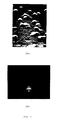
- Fig. 1 the surface condition and the crystallinity of the silicon films formed at various deposition temperatures are shown.
- the deposition was carried out by a low pressure chemical vapor deposition (LPCVD) method on a silicon substrate whose surface is covered with an SiO 2 film.
- LPCVD low pressure chemical vapor deposition
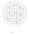
- 1AA, 1BA, 1CA, 1DA and 1EA are the scanning electron microscopy (SEM) photographs, with magnification of 100,000, of the surface of 2500 ⁇ -thick silicon films deposited at the temperatures of 550°C (510°C), 580°C (540°C), 590°C (550°C), 600°C (560°C) and 650°C (610°C), respectively.
- the space between the adjacent dots among a group of dots shown at the bottom of the photographs is 30 nm, and hence the distance from one end dot to the other end dot of the arrayed 11 dots is 300 nm.
- the acceleration voltage of the electron micrograph is 20 kV.
- Figs. 1AB, 1BB, 1CB, 1DB and 1EB are RHEED photographs that show crystallinity corresponding to Figs. 1AA, 1BA, 1CA, 1DA and 1EA, respectively.
- Fig. 1AA the surface of the silicon film deposited at 550°C (510°C) is very smooth, and no grain growth is observed.
- Fig. 1AB no ringlike patterns are visible in the RHEED photograph, Fig. 1AB, indicating that the film is amorphous.
- Fig. 1BA a partial growth of grains is observable, coexisting with the amorphous phase.
- Ringlike patterns appear in the RHEED photograph, Fig. 1BB, confirming a partial formation of crystals.
- the grain diameter becomes further increased with smooth surface as shown in Fig. 1EA, and there are observed the dots of reflection electron diffraction with the formation of polycrystalline silicon as shown in Fig. 1EB.
- a silicon film which is grown at the transition temperature where the crystal condition changes from the amorphous phase to the crystalline phase is considered to lack compactness to some extent. This is estimated from the fact that the etching rate, for example, by a wet etching method, of a silicon film grown at the transition temperature is higher than that of a polycrystalline silicon film deposited at an ordinary deposition temperature (a temperature higher than the transition temperature).
- a compact polycrystalline silicon film may be deposited on the above-mentioned silicon having micro roughness to such an extent of thickness that will not fill in the micro roughness.
- the compact polycrystalline silicon may be deposited at a temperature above 600°C (560°C).
- the transition temperature has a certain range.
- the grain diameter becomes large because the density of generation points of silicon nuclei on the surface of amorphous silicon is low.
- the grain diameter becomes small because the density of generation points of silicon nuclei on the surface of amorphous silicon is high.
- the size and the density of grains can also be controlled by varying the growth pressure of the silicon film within the range of the transition temperature. This is because the generation of the silicon nuclei on the surface of amorphous silicon is suppressed due to the mixing of hydrogen into the silicon film if the silicon film is deposited at a low vacuum. Because of this, the grain size becomes large. On the other hand, if a silicon film is deposited at a high vacuum, the mixing of hydrogen into the silicon film is decreased and the density of nucleus generation on the surface of amorphous silicon becomes high. Because of this, the grain size becomes small.
- the size and the density of the grains can be controlled by controlling the deposition pressure and the density of hydrogen for the silicon film within the range of transition temperature as described in the above. Further, even if the pressure is constant, it is possible to control the grain size and the grain density by changing the hydrogen concentration in amorphous silicon by varying the partial pressure of the material gases.
- a stacked capacitor was trially manufactured.
- a thick SiO 2 film was formed on a silicon substrate, a silicon film was formed on top of it in accordance with the method illustrated in Fig. 1, and the product was used as the lower electrode of the capacitor.
- Phosphorus was diffused into the silicon film obtained under the conditions of 820°C and 60 minutes, a capacitor insulating film was formed on the surface and a polycrystalline silicon film that is to become the upper electrode was formed on top of it.
- the formation of the capacitor insulating film was accomplished by first forming an Si 3 N 4 film on the silicon film by an LPCVD method, then by oxidizing the surface of the Si 3 N 4 film.
- the thickness of the capacitor insulating film is in the range of 30 to 500 ⁇ so as to enable the replication of the micro roughness of the lower layer silicon film onto the upper surface of the capacitor insulating film.
- the measurement was taken using the stacked capacitor of Embodiment 1.
- the numerical values which indicate the ratio of the surface area with respect to that of the wafer formed at 550°C (510°C) show that the surface area increase is very uniform all over the wafer surface.
- its reproducibility was also found to be satisfactory. This uniformity prevails also between wafers and between lots, and the reproducibility is also high.
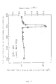
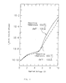
- Fig. 5 is shown the leakage current characteristic of the stacked capacitors obtained at the deposition temperatures of 590°C (550°C) and 640°C (600°C). It can be seen that the result for the former case is somewhat inferior to the latter case.
- the maximum voltage applied to a capacitor is 5 V (lately, 3.3 V). Therefore, there arises substantially no problem since there exists hardly any difference in the leakage current between the two cases up to the voltage of 5 V, and the applied voltage can be reduced to one half by the use of the well-known 1/2 Vcc cell plate technique.
- the leakage current characteristic will be compared when the same capacity is secured.
- a capacitor insulating film of about 50 ⁇ thickness when converted to equivalent oxide film (deff) is required if a polycrystalline silicon film deposited at the conventional temperature of about 640°C (600°C) is used as a storage electrode.
- deff equivalent oxide film
- a silicon film in accordance with the present invention it becomes possible to use a capacitor insulating film with thickness of 100 ⁇ .
- Fig. 6 are shown the leakage current characteristic for two representative cases.
- the voltage by which the leakage current can be suppressed to below 1 x 10 -8 A/cm 2 where a capacitor is usable as a device is 2.0 V for the conventional capacitor.
- the corresponding voltage can be increased to 5.4 V in the case of using silicon of the present embodiment, sharply improving the leakage current characteristic.
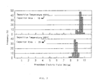
- Fig. 7 is shown the breakdown voltage distribution for the same cases of deposition at 590°C (550°C) and 640°C (600°C) that are given in the lower and upper portions of the figure, respectively.
- the results shown correspond to the measurements results taken by using stacked capacitors with the same structure as in Embodiment 1 for several sheets of wafer.
- the thickness of the capacitor insulating film at this time was 100 ⁇ .
- the peak value of the breakdown electric field intensity for the case of Si electrode deposition temperature at 590°C (550°C) is 8.7 MV/cm while the peak value for the case of 640°C (600°C) is 9.5 MV/cm so that the deterioration of the former case is 0.8 MV/cm relative to the latter.
- the scatter of the breakdown electric field intensity value is comparable for both samples, and is very satisfactory.
- the stacked capacitor used in the present embodiment was trially manufactured in the same way as in Embodiment 1.
- the quality of the silicon film deposited at the transition temperature was made compact by a heat treatment at the time of phosphorus diffusion.
- the film quality was made compact by subjecting the sample to an annealing at a temperature above the transition temperature prior to the formation of the capacitor insulating film.
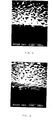
- Fig. 8 is shown an SEM photograph of the surface of a silicon film deposited at the transition temperature of 590°C (550°C), then annealed at 740°C (700°C) in a nitrogen atmosphere. There is little change in the surface condition from that at the time of the film deposition.
- the annealing was carried out at 740°C (700°C) in the present embodiment, but the compactification of the silicon film may be accomplished by an annealing for a long time at a low temperature such as 650°C (610°C) or by an annealing at a high temperature of 840°C (800°C).
- FIG. 9 is an SEM photograph showing the surface condition of the surface after the deposition. There is observed little change in the surface condition.
- a stacked capacitor was formed in the same way as in Embodiment 2, and the capacitance and the surface area of the capacitor formed were measured.
- the result is similar to that of Embodiment 1, their value distribution within the wafer, between wafers and between lots was extremely uniform, and its reproducibility was excellent. Further, the leakage current characteristic and the breakdown voltage were satisfactory, being substantially the same as those for the deposition temperature of 640°C (600°C).
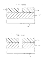
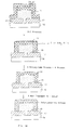
- a silicon oxide film 2 is formed on a silicon substrate 1 with a transfer gate and the like formed thereon, resist 3 is applied to be patterned and the oxide film 2 is etched by dry etching (Fig. 10b).
- a polycrystalline silicon film 4 is deposited, and an impurity such as phosphorus or arsenic is doped by thermal diffusion.
- the polycrystalline silicon film 4 is deposited by an LPCVD method under the normal conditions of the temperature of 640°C (600°C), reaction gas which is a mixture of SiH 4 and He (at 20 vol % of SiH 4 and 80 vol % of He) and pressure of 1 Torr.
- a silicon oxide film 5 is formed by a CVD method on the polycrystalline silicon film 4, and another polycrystalline silicon film 6 is formed on top of it under the same conditions as for the polycrystalline silicon film 4.
- a resist 7 is applied on top of it to be patterned (Fig. 10c), and by using the resist as a mask dryetching is given up to the polycrystalline silicon film 4 (Fig. 10d).
- a silicon film 8 having surface with a micro roughness is deposited at 595°C (555°C) (Fig. 10e).
- the deposition conditions are the same as for the polycrystalline silicon film 4 except for the temperature.
- the sample is annealed at 740°C (700°C) for 30 minutes in a nitrogen atmosphere.
- phosphorus or arsenic is doped into the silicon film 8 by thermal diffusion.
- the sample is subjected to a reactive ion etching (RIE) that uses Cl 2 gas to obtain a lower electrode 8 for a stacked capacitor as shown in Fig. 10f.
- RIE reactive ion etching
- the top portion and the side faces of the silicon film 18 have even after the RIE a roughness with large area that reflects the roughness before the etching of the silicon film 8.
- the top portion and the side faces of the silicon film 18 are given a roughness by the replication of the roughness of the silicon film 8 onto the polycrystalline silicon film 6. Note that in the absence of the polycrystalline silicon film 6 the top portion of the stacked capacitor will be lost at the time of RIE and there will be left only its side faces.
- a capacitor insulating film 9 is formed under the same conditions as for Embodiment 1, and further a phosphorus-doped polycrystalline silicon film 10 is deposited (Fig. 10g).
- a stacked capacitor that has a capacitor parts formed also on the side faces and has a very large capacitance can be obtained.
- Figs. 11a and 11b are shown the SEM photographs of the stacked capacitor formed. The magnifications of Figs. 11a and 11b are 40,000 and 25,000, respectively, showing approximately the same location of the capacitors.
- One of the forefront capacitors is revealing its cross section. From the figure it can be seen that there still remains a sufficiently well-defined roughness on the surface of the silicon film even after the dry etching.
- phosphosilicate glass PSG
- borophosphosilicate glass BPSG
- an impurity-doped polycrystalline silicon film a silicon nitride film, a laminated film of some of the foregoings, or the like may be employed in place of the oxide film 5.
- the silicon film 8 having a micro roughness in Fig. 10f was subjected as it is to an RIE.
- RIE high temperature oxidation
- the polycrystalline silicon film 6 formed at the temperature of 640°C (600°C) was used as a film for replicating the micro roughness on the silicon film 8, but the film 6 may be replaced by a silicon film deposited at or below the transition temperature.
- thermal diffusion was employed invariably for the doping to the silicon film, but there may be used ion implantation or a method in which a dopant gas such as PH 3 or AsH 3 is included in the material gas at the time of deposition may also be employed.
- the dopant may be boron besides phosphorus and arsenic.
- Embodiments 1 to 4 an example has been shown in which a micro roughness is formed all over the surface of the portions of the silicon films 6 and 8 that are to become a capacitor, but the capacitance will become larger than the case of the conventional flat polycrystalline silicon film even when the micro roughness is formed even in a portion of the film.
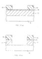
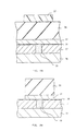
- a silicon film having a surface with a micro roughness can also be formed by first forming an amorphous silicon layer on a substrate, then by annealing the amorphous silicon layer at a temperature above the transition temperature. This phenomenon will be described by reference to Fig. 12.
- a flat a-Si film 12 is deposited on a substrate such as a silicon substrate whose surface is covered with an SiO 2 film as shown in Fig. 12a.
- a vacuum higher than 1 x 10 -6 Torr or in an inest gas at a temperature above the transition temperature while maintaining the substrate surface clean polycrystalline silicon nuclei 13 are formed on the surface as shown in Fig. 12b.
- the diffusion rate of silicon on the clean a-Si surface is extremely high compared with the growth rate of the a-Si solid phase, and silicon atoms are collected around the polycrystalline silicon nuclei formed on the surface by their diffusion in the surface, and the polycrystalline silicon nuclei 14 grow in mushroom like shape or hemisphere like shape as shown in Fig. 12c. The growth of the nuclei 14 are continued. Finally as shown in Fig. 12d the nuclei become the grains 15 which have hemisphere like shape.
- the annealing temperature for the forming of the micro roughness on the Si surface will not give any substantial influence provided that it is above the transition temperature. However, rapid heating at a high temperature of such as 900°C is not recommended. This is because under such an annealing, crystallization starts from not only the surface of the amorphous silicon film 12 but also the interior of it, making it impossible to grow the nuclei and obtain a substantial micro roughness on the surface. It is necessary to grow polycrystalline silicon nuclei 13 first on the surface of the amorphous silicon film 12. For that purpose, it is preferable that the annealing is given in the range of 580 to 750°C.
- the average size and the density of the grain projections formed from the surface of the amorphous silicon surface by changing the temperature of the heat treatment the amorphous silicon film in a nonoxidizing atmosphere, such as in a vacuum, in an inert gas or nitrogen gas.
- a nonoxidizing atmosphere such as in a vacuum
- an inert gas or nitrogen gas for the growth of silicon grains from the surface of the amorphous silicon film it is first necessary to form nuclei which will act as the seeds for growing grains on the surface of the amorphous silicon film.
- the heating temperature substantially changes the density at which these nuclei are formed. When the heating temperature is high, this density becomes high, and the average size of the grain projections formed on the surface of the silicon film becomes small and the density of the projections becomes high.
- the heating temperature When the heating temperature is low, the density of nucleus generation is low. Because of this, the number of silicon atoms supplied to each nuclei at the time of grain growth becomes high compared with the heating at high temperature. Accordingly, in the case of heating at low temperature, each grain grows into a large size, making the average diameter of the projections large and the density of the projections small. Moreover, the average size and the density of the grain projections formed from the surface of the amorphous silicon film, at the time of forming a micro roughness through the formation of silicon nuclei from the surface of the amorphous silicon film, can also be changed by varying the rate of temperature rise in the vicinity of the temperature of silicon nuclei formation.
- the average size and the density of the grain projections formed from the surface of the amorphous silicon surface can also be changed by varying the hydrogen concentration within the amorphous silicon film instead of controlling the grain size by changing the heating temperature.
- these dangling bonds can be terminated by means of hydron atoms.
- these hydrogen atoms drop off, bringing some of the silicon atoms to a stably bonded state. Accordingly, when hydrogen is added at high concentration, the generation density of the nuclei becomes low, each grain grows to a large size, and the average diameter of the projections becomes large and the surface grain density becomes low.
- concentration of hydron addition is made low, the generation density of the nuclei becomes high, the average diameter of the grain projections becomes small and the density becomes high.
- silicon atoms can also sufficiently freely migrate in the surface of the amorphous silicon film when impurities are added to the amorphous silicon film, and a phenomenon analogous to the case of not adding impurities to the amorphous silicon layer can be induced.
- a polycrystalline silicon film having a surface with a micro roughness can also be formed by the aforementioned methods.
- a roughness cannot be formed on the surface even if the sample is subjected to an annealing when the surface of the amorphous silicon film 12 is covered with a native oxidized film or impurities such as carbon atoms are attached to the surface. Consequently, when the film 12 is to be processed to a predetermined shape subsequent to the formation of the film 12, annealing has to be given following the formation of the surface of the amorphous silicon film after the processing, although there will be no problem if the formation of the amorphous silicon film 12 and the subsequent annealing are carried out in the same furnace tube.
- An amorphous silicon film was formed using a molecular beam epitaxy (MBE) apparatus that is equipped with an electron gun type silicon evaporator with a volume of 40 cm 3 .
- MBE molecular beam epitaxy
- For the sample wafer use was made of a 4-inch n-type silicon (100) substrate on which is formed a 2000 ⁇ -thick SiO 2 film by thermal oxidation. After an RCA washing the sample wafer is transferred to the interior of a formation chamber, and a cleaning was given by heating it at 800°C for one minute. After lowering the substrate temperature to room temperature, the sample was irradiated with a silicon molecular beam of 7 ⁇ /s from the electron gun type silicon evaporator to form a 2000 ⁇ -thick a-Si layer on the oxide film.
- the a-Si layer was converted to a polycrystalline silicon layer by heating the substrate in a vacuum higher than 1 x 10 -6 Torr, in an inert gas or in a N 2 gas with impurity concentration equivalent to that degree of vacuum, by heating the substrate in the same vacuum chamber. Whether the polycrystallization was accomplished or not was judged by an in-situ observation by RHEED technique.
- the substrate formed was taken out into the atmosphere, and it was evaluated by observing the cross section by means of the transmission electron microscopy (TEM).
- a lower electrode for a stacked capacitor was formed under the same conditions as in the present embodiment. Namely, a wafer with an a-Si layer formed on an SiO 2 film that covers a silicon substrate was taken out of an apparatus, and was processed into a cylindrical form as shown in Fig. 13(a). The processed a-Si layer was covered with and this oxidized film was removed, from the surface of the a-Si layer and its surface was cleaned. And the substrate was subjected to an annealing in an argon atmosphere. As a result, there was obtained a polycrystalline silicon film having a surface with a micro roughness as shown in Fig. 13(b).
- a capacitor was manufactured by forming a 100 ⁇ -thick oxide film on the polycrystalline silicon film thus formed, and its capacitance was measured.
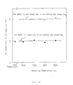
- Fig. 14 shows the dependence of the capacitance on the annealing temperature after the deposition of the a-Si film for the case of taking the sample out into the atmosphere before the annealing and the case of not doing so. As shown in Fig. 14, when the sample was not taken out into the atmosphere, a capacitance which is about twice as large that of the case of taking it out into the atmosphere was obtained for a very wide range of annealing temperature, after the a-Si film was annealed.
- the capacitance does not increase by annealing, remaining at substantially the same value as at immediately after the formation of the a-Si film.
- the a-Si film covered with an oxide film have the similar capacitance value to a polycrystalline silicon film which is used directly to form a lower electrode according to the conventional method.
- the annealing was given in an argon atmosphere in the present embodiment, it can be given in helium (He), in nitrogen (N 2 ) or in a vacuum of higher than 1 x 10 -6 Torr.
- the present embodiment can be applied to a silicon on sapphire (SOS) substrate or a silicon on insulator (SOI) substrate instead of to a silicon substrate.
- the a-Si layer was formed in an MBE apparatus using an electron gun type silicon evaporation device.
- a phenomenon similar to the above occurs also in other methods of a-Si layer formation such as a gas source MBE method, an LPCVD method and a sputtering method provided that the a-Si layer surface is clean.
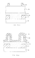
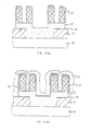
- Fig. 15(a) an oxide film 17 was formed on a silicon substrate 16 and a resist 18 was applied on the surface to be patterned. Then, the oxide film 17 was given a dry etching (Fig. 15(b)). Then, as shown in Fig. 15(c), a polycrystalline silicon 19 was deposited and an impurity such as phosphorus or arsenic was doped by thermal diffusion.
- the polycrystalline silicon film 19 was deposited by an LPCVD method under the ordinary conditions of a temperature of 600°C and a pressure of 1 Torr using a mixed gas of SiH 4 and He (at 20 vol % of SiH 4 and 80 vol % of He).
- An amorphous silicon film 20 was deposited on top of it at 500°C.
- the growth conditions other than that of the temperature are the same as for the case of deposition of the polycrystalline silicon film at 600°C.
- the amorphous silicon film was coated with a resist 21 and patterned (Fig. 15(c)). Then the amorphous silicon film 20 and the polycrystalline silicon film 19 were dry etched using the resist 21 as a mask (Fig. 15(d)).
- an amorphous silicon film 22 was deposited by an LPCVD method to a thickness of 2000 ⁇ (Fig. 15(e)).
- the deposition conditions were a temperature 510°C, a mixed gas of SiH 4 and He (at 20 vol % of SiH 4 and 80 vol % of He) and a pressure of 1 Torr.
- the amorphous silicon film 22 was processed by RIE to form an electrode (Fig. 15(f)).
- the surface was washed with a mixed solution of ammonia and hydrogen peroxide in order to remove carbon contamination on the amorphous silicon film 22, and further, a natine oxide film was removed using HF or etching.
- the sample was introduced into a vacuum of 1 x 10 -7 Torr to be heated at 600°C for one hour.
- a micro roughness was formed on the electrode surface (Fig. 15(g)).
- the electrode was heated at about 800°C.
- a conductive impurity such as phosphorus or arsenic is injected from the lower electrode into the silicon film that has a micro roughness.
- a capacitor insulating film 23 and an upper electrode 24 were formed (Fig. 15(h)).
- the factor of surface area increase of the capacitor formed as in the above is very high being about 2.1 times that of a silicon film deposited in accordance with the conventional method.
- carbon atoms may have a chance of being attached to the surface of the amorphous silicon film after the RIE treatment. If carbon atoms remain on the amorphous silicon surface, a micro roughness will not be formed on the surface of the amorphous silicon even if it is heated in vacuum, because the surface migration of the silicon atoms is restrained by the carbon atoms. These carbon atoms may be removed by washing with a mixed solution of ammonia and hydrogen peroxide.
- an optical surface treatment method that uses a halogen gas may be adopted to simultaneously remove carbons, the spontaneously oxidized film and the portions of the silicon film sustained damage by the RIE from the amorphous silicon film after the RIE.
- Chlorine gas may be used as the halogen gas.
- the lamp to be used may be a mercury lamp of wavelength 300 to 400 nm operated at 200 m Torr and power of 110 mW/cm 2 .
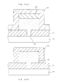
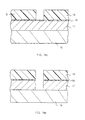
- a silicon nitride film 25 and an oxide film 17 were formed on a silicon substrate 16. Then a resist 26 was applied to the surface and patterned. Then the oxide film 17 and the silicon nitride film 25 were dry etched, as shown in Fig. 17(b). The resist 16 was removed.
- a polycrystalline silicon film 27 was deposited as shown in Fig. 17(c) by an LPCVD method under the ordinary conditions of a temperature of 600°C, a reaction gas which is a mixture of SiH 4 and He (at 20 vol % of SiH 4 and 80 vol % of He) and at a pressure of 1 Torr. Then an impurity such as phosphorus or arsenic was doped by thermal diffusion.
- An high temperature oxide (HTO) CVD oxide film 28 was deposited on top of it to a thickness of 4000 ⁇ under the deposition conditions of a temperature of 600°C, a reaction gas which is a mixture of SiH 4 , He (at 20 vol % of SiH 4 and 80 vol % of He) and N 2 O gas (in the flow rate of one in SiH 4 + He to five in N 2 O) and a pressure of 1 Torr.
- a resist 29 was applied on the surface of the oxide film 28 and then patterned (Fig. 17(c)). The oxide film 28 was dry-fetched using the resist 29 as a mask. Then the resist 29 was removed and an amorphous silicon film 30 was deposited to a thickness of 1500 ⁇ (Fig. 17(d)).
- the amorphous silicon 30 and a part of polycrystalline silicon film 27 was processed by RIE to form an electrode (Fig. 17(e)). Then, the carbon contamination on the amorphous silicon film was removed by washing with a mixed solution of ammonia and hydrogen peroxide. Then the spontaneously oxidized film was removed by using HF. Next, the sample was introduced to a vacuum of 1 x 10 -7 Torr and was subjected to a heat treatment at 600°C for one hour. A micro roughness was formed on the electrode surface by this heat treatment (Fig. 17(f)). Then the oxide film 28 between the pieces of the electrode 31 was removed by wet etching by using a mixed solution of HF and water in the ratio of 1 to 100. Finally, a capacitor was completed by depositing a capacitor insulating film 32 and a phosphorus-doped polycrystalline silicon film 33 (Fig. 17(g) and 17(h)).
- This embodiment shows the method for fabricating cylinder like shaped electrode having micro roughness on the surface.
- This electrode serves as a stacked capacitor electrode.
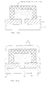
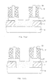
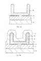
- a silicon oxide film 17 is formed on a silicon substrate 16.
- a silicon nitride film 34 is formed on the silicon oxide film 17 and a resist 18 is coated on this film 34 and patterned.
- the silicon nitride film 34 and the silicon oxide film 17 are etched by dry etching, and thereafter the resist 18 is removed (Fig. 18b).
- a polycrystalline silicon film 19 is deposited, and an impurity such as phosphorus or arsenic is doped by thermal diffusion.
- the polycrystalline silicon film 19 is etched back till the upper surface of the silicon nitride film 34 is exposed, and it is remained only in the through hole of the silicon oxide film 17.
- an amorphous silicon film 35 is deposited on the silicon nitride film 34 and a silicon oxide film 36 is deposited by the CVD method at the temperature of 550°C (510°C).
- the thickness of the silicon oxide film 36 is defined by the height of the desired electrode.
- a resist 37 is coated on the silicon oxide film 36 and patterned. Using the resist 37 as a mask, the silicon oxide film 36 and the amorphous silicon 35 are etched by dry etching and the resist 37 is removed (Fig. 18d).
- an amorphous silicon film 37 is deposited on the silicon oxide film 36 and the amorphous silicon film 35 by the same fabrication method of the amorphous silicon film 35 (Fig. 18e). Then, the amorphous silicon film 37 is etched back till the top surface of the silicon oxide film 36 is exposed (Fig. 18f). Then the silicon oxide film 36 is removed by the HF process. But this process produces a native oxide film on the amorphous silicon 35, 37. To remove the native oxide film, this film is washed with a mixed solution of ammonia and hydrogen peroxide and washed with the solution of HF.
- the sample is annealed under the condition of a temperature of 600°C, a pressure of 1 Torr and an annealing time of 10 minutes.
- the amorphous silicon 35, 37 become a polycrystalline silicon 38 have the micro roughness on its surface (Fig. 18g).
- Fig. 19 is a scanning electron microscopy photograph of the real sample of Fig. 18g.
- the sample is taken out in air, the sample is ion implanted under the condition of a concentration of phosphorus 10 20 atoms/cm 3 and an angle of incidence 7 degrees, so that the surface part of the polycrystalline silicon 38 contains a high concentration of phosphorus.
- a capacitor insulating film 39 is formed on the polycrystalline silicon 38 and a phosphorus-doped polycrystalline silicon film 40 is deposited (Fig. 18h).
- the silicon nitride film 34 may be omitted and the amorphous silicon film 35 may be deposited on the surface of the silicon oxide film 17.
- the shape of the storage electrode with a micro roughness for a stacked capacitor may be a plain cubic structure, a cylindrical structure, a fin-type structure or a stacked trench type.
Description
Claims (5)
- A method of fabricating a semiconductor device having a capacitor, comprising the steps of:depositing an amorphous silicon layer (22) on a substrate (16,17,19,20);cleaning a surface of said amorphous silicon;annealing said amorphous silicon layer while keeping the surface of said amorphous silicon layer clean at a temperature above a transition temperature from an amorphous phase to a polycrystalline phase of silicon to thereby convert said amorphous silicon layer into a polycrystalline silicon layer, said polycrystalline silicon layer thereby having a micro-roughness surface caused by grains of silicon and serving as a first electrode of said capacitor;forming a dielectric film (23) of said capacitor on said micro-roughness surface of said polycrystalline silicon layer; andforming on said dielectric film a conductive layer (24) serving as a second electrode of said capacitor.
- The method as claimed in Claim 1, wherein said step of cleaning comprises the step of removing a natural oxide film formed on said amorphous silicon layer.
- The method as claimed in Claim 1 or 2, wherein said transition temperature is in a range of 580 to 600°C.
- The method as claimed in Claim 1, 2 or 3, wherein said dielectric film has a thickness in the range 3 to 50 nm.
- The method as claimed in Claim 1, 2, 3 or 4, wherein a size of each of said grains of silicon is in a range of 30 to 170 nm in diameter.
Applications Claiming Priority (7)
| Application Number | Priority Date | Filing Date | Title |
|---|---|---|---|
| JP2072462A JP2937395B2 (en) | 1990-03-20 | 1990-03-20 | Semiconductor element |
| JP72462/90 | 1990-03-20 | ||
| JP2249154A JP2861343B2 (en) | 1990-09-19 | 1990-09-19 | Semiconductor device and manufacturing method thereof |
| JP249154/90 | 1990-09-19 | ||
| JP327069/90 | 1990-11-28 | ||
| JP2327069A JP2800408B2 (en) | 1990-11-28 | 1990-11-28 | Method for manufacturing semiconductor device |
| EP91302414A EP0448374B1 (en) | 1990-03-20 | 1991-03-20 | Method for fabricating a semiconductor device having a capacitor with polycrystalline silicon having micro roughness on the surface |
Related Parent Applications (2)
| Application Number | Title | Priority Date | Filing Date |
|---|---|---|---|
| EP91302414A Division EP0448374B1 (en) | 1990-03-20 | 1991-03-20 | Method for fabricating a semiconductor device having a capacitor with polycrystalline silicon having micro roughness on the surface |
| EP91302414.7 Division | 1991-03-20 |
Publications (3)
| Publication Number | Publication Date |
|---|---|
| EP0630055A2 EP0630055A2 (en) | 1994-12-21 |
| EP0630055A3 EP0630055A3 (en) | 1995-01-04 |
| EP0630055B1 true EP0630055B1 (en) | 1998-09-23 |
Family
ID=27300963
Family Applications (3)
| Application Number | Title | Priority Date | Filing Date |
|---|---|---|---|
| EP91302414A Expired - Lifetime EP0448374B1 (en) | 1990-03-20 | 1991-03-20 | Method for fabricating a semiconductor device having a capacitor with polycrystalline silicon having micro roughness on the surface |
| EP95110516A Expired - Lifetime EP0689252B1 (en) | 1990-03-20 | 1991-03-20 | Semiconductor device |
| EP94111698A Expired - Lifetime EP0630055B1 (en) | 1990-03-20 | 1991-03-20 | Method for fabricating polycrystalline silicon having micro roughness on the surface |
Family Applications Before (2)
| Application Number | Title | Priority Date | Filing Date |
|---|---|---|---|
| EP91302414A Expired - Lifetime EP0448374B1 (en) | 1990-03-20 | 1991-03-20 | Method for fabricating a semiconductor device having a capacitor with polycrystalline silicon having micro roughness on the surface |
| EP95110516A Expired - Lifetime EP0689252B1 (en) | 1990-03-20 | 1991-03-20 | Semiconductor device |
Country Status (4)
| Country | Link |
|---|---|
| US (2) | US5366917A (en) |
| EP (3) | EP0448374B1 (en) |
| KR (1) | KR960012915B1 (en) |
| DE (3) | DE69130263T2 (en) |
Families Citing this family (147)
| Publication number | Priority date | Publication date | Assignee | Title |
|---|---|---|---|---|
| US5244842A (en) * | 1991-12-17 | 1993-09-14 | Micron Technology, Inc. | Method of increasing capacitance by surface roughening in semiconductor wafer processing |
| GB2293691B (en) * | 1991-09-07 | 1996-06-19 | Samsung Electronics Co Ltd | Semiconductor memory devices |
| US5350707A (en) * | 1991-11-19 | 1994-09-27 | Samsung Electronics Co., Ltd. | Method for making a capacitor having an electrode surface with a plurality of trenches formed therein |
| US5191509A (en) * | 1991-12-11 | 1993-03-02 | International Business Machines Corporation | Textured polysilicon stacked trench capacitor |
| EP0553791A1 (en) * | 1992-01-31 | 1993-08-04 | Nec Corporation | Capacitor electrode for dram and process of fabrication thereof |
| KR960002097B1 (en) * | 1992-02-28 | 1996-02-10 | 삼성전자주식회사 | Method of making a capacitor for a semiconductor device |
| US5278091A (en) * | 1993-05-04 | 1994-01-11 | Micron Semiconductor, Inc. | Process to manufacture crown stacked capacitor structures with HSG-rugged polysilicon on all sides of the storage node |
| DE4419074C2 (en) * | 1993-06-03 | 1998-07-02 | Micron Semiconductor Inc | Method for uniformly doping polycrystalline silicon with hemispherical grain |
| US6328794B1 (en) * | 1993-06-26 | 2001-12-11 | International Business Machines Corporation | Method of controlling stress in a film |
| US5656531A (en) * | 1993-12-10 | 1997-08-12 | Micron Technology, Inc. | Method to form hemi-spherical grain (HSG) silicon from amorphous silicon |
| US5972771A (en) | 1994-03-11 | 1999-10-26 | Micron Technology, Inc. | Enhancing semiconductor structure surface area using HSG and etching |
| JP2697645B2 (en) * | 1994-10-31 | 1998-01-14 | 日本電気株式会社 | Method for manufacturing semiconductor device |
| US6121081A (en) * | 1994-11-15 | 2000-09-19 | Micron Technology, Inc. | Method to form hemi-spherical grain (HSG) silicon |
| KR0165499B1 (en) * | 1995-01-26 | 1998-12-15 | Samsung Electronics Co Ltd | Capacitor fabrication method of semiconductor device |
| JP2689935B2 (en) * | 1995-02-01 | 1997-12-10 | 日本電気株式会社 | Semiconductor thin film forming method |
| KR0165496B1 (en) * | 1995-03-22 | 1998-12-15 | 윤종용 | Capacitor fabrication method of high integrated semiconductor device |
| KR960039197A (en) * | 1995-04-12 | 1996-11-21 | 모리시다 요이치 | Method of forming silicon oxide film and method of manufacturing semiconductor device |
| US5508223A (en) * | 1995-05-05 | 1996-04-16 | Vanguard International Semiconductor Corporation | Method for manufacturing DRAM cell with fork-shaped capacitor |
| US5597754A (en) * | 1995-05-25 | 1997-01-28 | Industrial Technology Research Institute | Increased surface area for DRAM, storage node capacitors, using a novel polysilicon deposition and anneal process |
| KR100295718B1 (en) * | 1995-06-06 | 2001-09-03 | 아사히 가세이 마이크로시스템 가부시끼가이샤 | Semiconductor device and method of production thereof |
| US5663090A (en) * | 1995-06-29 | 1997-09-02 | Micron Technology, Inc. | Method to thermally form hemispherical grain (HSG) silicon to enhance capacitance for application in high density DRAMs |
| US5856007A (en) * | 1995-07-18 | 1999-01-05 | Sharan; Sujit | Method and apparatus for forming features in holes, trenches and other voids in the manufacturing of microelectronic devices |
| US5885882A (en) * | 1995-07-18 | 1999-03-23 | Micron Technology, Inc. | Method for making polysilicon electrode with increased surface area making same |
| US6187628B1 (en) * | 1995-08-23 | 2001-02-13 | Micron Technology, Inc. | Semiconductor processing method of forming hemispherical grain polysilicon and a substrate having a hemispherical grain polysilicon layer |
| US5639685A (en) * | 1995-10-06 | 1997-06-17 | Micron Technology, Inc. | Semiconductor processing method of providing a conductively doped layer of hemispherical grain polysilicon |
| US6638818B1 (en) * | 1995-10-06 | 2003-10-28 | Texas Instruments Incorporated | Method of fabricating a dynamic random access memory with increased capacitance |
| KR100224710B1 (en) | 1995-10-10 | 1999-10-15 | 윤종용 | Method for manufacturing of capacitor in semiconductor device |
| US5801104A (en) * | 1995-10-24 | 1998-09-01 | Micron Technology, Inc. | Uniform dielectric film deposition on textured surfaces |
| US5612558A (en) | 1995-11-15 | 1997-03-18 | Micron Technology, Inc. | Hemispherical grained silicon on refractory metal nitride |
| US5801413A (en) * | 1995-12-19 | 1998-09-01 | Micron Technology, Inc. | Container-shaped bottom electrode for integrated circuit capacitor with partially rugged surface |
| US6015986A (en) * | 1995-12-22 | 2000-01-18 | Micron Technology, Inc. | Rugged metal electrodes for metal-insulator-metal capacitors |
| KR100224707B1 (en) * | 1995-12-23 | 1999-10-15 | 윤종용 | Method for manufacturing of semiconductor device capacitor |
| US5830793A (en) * | 1995-12-28 | 1998-11-03 | Micron Technology, Inc. | Method of selective texfturing for patterned polysilicon electrodes |
| US6331457B1 (en) * | 1997-01-24 | 2001-12-18 | Semiconductor Energy Laboratory., Ltd. Co. | Method for manufacturing a semiconductor thin film |
| JP2795313B2 (en) * | 1996-05-08 | 1998-09-10 | 日本電気株式会社 | Capacitive element and method of manufacturing the same |
| US6027970A (en) | 1996-05-17 | 2000-02-22 | Micron Technology, Inc. | Method of increasing capacitance of memory cells incorporating hemispherical grained silicon |
| KR100219482B1 (en) * | 1996-05-23 | 1999-09-01 | 윤종용 | Method for capacitor in semiconductor device |
| EP0810653B1 (en) * | 1996-05-31 | 2004-07-28 | Texas Instruments Incorporated | DRAM and method of fabricating a DRAM with increased capacity |
| KR100235938B1 (en) * | 1996-06-24 | 1999-12-15 | 김영환 | A fabrication method of semicircle silicon |
| KR100230363B1 (en) * | 1996-06-28 | 1999-11-15 | 윤종용 | Method for manufacturing capacitor of semiconductor device |
| US6190992B1 (en) | 1996-07-15 | 2001-02-20 | Micron Technology, Inc. | Method to achieve rough silicon surface on both sides of container for enhanced capacitance/area electrodes |
| US5849624A (en) * | 1996-07-30 | 1998-12-15 | Mircon Technology, Inc. | Method of fabricating a bottom electrode with rounded corners for an integrated memory cell capacitor |
| US5888295A (en) * | 1996-08-20 | 1999-03-30 | Micron Technology, Inc. | Method of forming a silicon film |
| US5960279A (en) * | 1996-08-27 | 1999-09-28 | Mosel Vitellic Incorporated | Method of fabricating a capacitor on a rugged stacked oxide layer |
| JP2953407B2 (en) * | 1996-10-21 | 1999-09-27 | 日本電気株式会社 | Method for manufacturing semiconductor device |
| US6528436B1 (en) * | 1996-10-21 | 2003-03-04 | Micron Technology. Inc. | Method of forming silicon nitride layer directly on HSG polysilicon |
| US5770500A (en) * | 1996-11-15 | 1998-06-23 | Micron Technology, Inc. | Process for improving roughness of conductive layer |
| KR100269287B1 (en) * | 1996-11-22 | 2000-11-01 | 윤종용 | A method for forming hemi-spherical grain |
| US5798280A (en) * | 1996-12-02 | 1998-08-25 | Micron Technology, Inc. | Process for doping hemispherical grain silicon |
| GB2320133B (en) * | 1996-12-04 | 2001-10-24 | United Microelectronics Corp | A method for increasing capacitance |
| US6060354A (en) * | 1996-12-20 | 2000-05-09 | Texas Instruments Incorporated | In-situ doped rough polysilicon storage cell structure formed using gas phase nucleation |
| US6117692A (en) * | 1997-01-14 | 2000-09-12 | Kim; Young-Sun | Calibrated methods of forming hemispherical grained silicon layers |
| JPH10242417A (en) * | 1997-02-25 | 1998-09-11 | Oki Electric Ind Co Ltd | Semiconductor device and its manufacturing method |
| US6069053A (en) * | 1997-02-28 | 2000-05-30 | Micron Technology, Inc. | Formation of conductive rugged silicon |
| US5937314A (en) | 1997-02-28 | 1999-08-10 | Micron Technology, Inc. | Diffusion-enhanced crystallization of amorphous materials to improve surface roughness |
| US6699745B1 (en) * | 1997-03-27 | 2004-03-02 | Texas Instruments Incorporated | Capacitor and memory structure and method |
| KR100259038B1 (en) * | 1997-03-31 | 2000-06-15 | 윤종용 | Method for manufacturing semiconductor capacitor and semiconductor capacitor manufactured thereby |
| KR100255662B1 (en) | 1997-05-03 | 2000-05-01 | 윤종용 | Method for manufacturing semiconductor device having polysilicon layer of hemisphere grain |
| KR100247931B1 (en) * | 1997-05-21 | 2000-03-15 | 윤종용 | Method for manufacturing semiconductor device having hsg-si layer |
| US6245632B1 (en) | 1997-05-22 | 2001-06-12 | Samsung Electronics Co., Ltd. | Variable temperature methods of forming hemispherical grained silicon (HSG-Si) layers |
| US5907774A (en) * | 1997-05-29 | 1999-05-25 | Texas Instruments Incorporated | Corrugated post capacitor and method of fabricating using selective silicon deposition |
| US6066576A (en) * | 1997-06-04 | 2000-05-23 | Micron Technology, Inc. | Method for forming oxide using high pressure |
| JP3149910B2 (en) * | 1997-06-05 | 2001-03-26 | 日本電気株式会社 | Method for manufacturing semiconductor device |
| KR100234380B1 (en) * | 1997-06-11 | 1999-12-15 | 윤종용 | Manufacturing method of semiconductor device having hsg-si layer |
| US6249019B1 (en) | 1997-06-27 | 2001-06-19 | Micron Technology, Inc. | Container capacitor with increased surface area and method for making same |
| KR100253086B1 (en) * | 1997-07-25 | 2000-04-15 | 윤종용 | Cleaning composition for semiconductor device and fabrication method of semiconductor device using said cleaning composition |
| US6048763A (en) * | 1997-08-21 | 2000-04-11 | Micron Technology, Inc. | Integrated capacitor bottom electrode with etch stop layer |
| US5920763A (en) * | 1997-08-21 | 1999-07-06 | Micron Technology, Inc. | Method and apparatus for improving the structural integrity of stacked capacitors |
| JP3796030B2 (en) | 1997-11-16 | 2006-07-12 | キヤノンアネルバ株式会社 | Thin film production equipment |
| KR100258096B1 (en) * | 1997-12-01 | 2000-06-01 | 정선종 | Manufacturing method of soi substrate |
| US5885867A (en) * | 1997-12-03 | 1999-03-23 | Samsung Electronics Co., Ltd. | Methods of forming hemispherical grained silicon layers including anti-nucleation gases |
| US6004858A (en) * | 1997-12-11 | 1999-12-21 | Samsung Electronics Co., Ltd. | Methods of forming hemispherical grained silicon (HSG-Si) capacitor structures including protective layers |
| JPH11214646A (en) * | 1998-01-28 | 1999-08-06 | Mitsubishi Electric Corp | Semiconductor memory and manufacture thereof |
| US6087226A (en) * | 1998-03-26 | 2000-07-11 | Samsung Electronics Co., Ltd. | Methods of forming capacitors including electrodes with hemispherical grained silicon layers on sidewalls thereof and related structures |
| KR100327123B1 (en) | 1998-03-30 | 2002-08-24 | 삼성전자 주식회사 | A method of fabricating dram cell capacitor |
| KR100265329B1 (en) | 1998-04-22 | 2000-09-15 | 김영환 | Method of forming selective hsg storage node in semiconductor device |
| EP0954030A1 (en) * | 1998-04-30 | 1999-11-03 | Siemens Aktiengesellschaft | Process of manufacturing a capacitor for a semiconductor memory |
| JP3161523B2 (en) * | 1998-05-14 | 2001-04-25 | 日本電気株式会社 | Method for manufacturing semiconductor device |
| US6355536B1 (en) | 1998-06-08 | 2002-03-12 | Micron Technology, Inc. | Selective method to form roughened silicon |
| TW429618B (en) * | 1998-08-01 | 2001-04-11 | United Microelectronics Corp | Fabricating method for the capacitor of dynamic random access memory |
| KR100282709B1 (en) * | 1998-08-28 | 2001-03-02 | 윤종용 | Manufacturing method of capacitor using hemispherical silicon |
| GB2341271B (en) * | 1998-09-01 | 2001-04-18 | United Semiconductor Corp | Method of fabricating capacitor |
| US6004857A (en) * | 1998-09-17 | 1999-12-21 | Taiwan Semiconductor Manufacturing Company | Method to increase DRAM capacitor via rough surface storage node plate |
| US6136660A (en) * | 1998-09-28 | 2000-10-24 | Siemens Aktiengesellschaft | Stacked capacitator memory cell and method of fabrication |
| US6303956B1 (en) * | 1999-02-26 | 2001-10-16 | Micron Technology, Inc. | Conductive container structures having a dielectric cap |
| US6358793B1 (en) | 1999-02-26 | 2002-03-19 | Micron Technology, Inc. | Method for localized masking for semiconductor structure development |
| US6764916B1 (en) * | 1999-03-23 | 2004-07-20 | Hitachi Kokusai Electric Inc. | Manufacturing method for semiconductor device |
| KR100316523B1 (en) * | 1999-04-23 | 2001-12-12 | 김영환 | Fabricating method of capacitor |
| KR100316524B1 (en) * | 1999-04-29 | 2001-12-12 | 김영환 | Fabricating method of capacitor |
| JP4655321B2 (en) * | 1999-08-27 | 2011-03-23 | 東京エレクトロン株式会社 | Heat treatment method |
| US6559007B1 (en) * | 2000-04-06 | 2003-05-06 | Micron Technology, Inc. | Method for forming flash memory device having a tunnel dielectric comprising nitrided oxide |
| DE10034005A1 (en) * | 2000-07-07 | 2002-01-24 | Infineon Technologies Ag | Process for creating micro-roughness on a surface |
| DE10038378A1 (en) | 2000-08-07 | 2002-02-28 | Infineon Technologies Ag | Process for the production of capacitor electrodes |
| US6455372B1 (en) | 2000-08-14 | 2002-09-24 | Micron Technology, Inc. | Nucleation for improved flash erase characteristics |
| US6639266B1 (en) | 2000-08-30 | 2003-10-28 | Micron Technology, Inc. | Modifying material removal selectivity in semiconductor structure development |
| US6544908B1 (en) | 2000-08-30 | 2003-04-08 | Micron Technology, Inc. | Ammonia gas passivation on nitride encapsulated devices |
| JP2002076293A (en) * | 2000-09-01 | 2002-03-15 | Matsushita Electric Ind Co Ltd | Method for manufacturing capacitor and semiconductor device |
| US20020182893A1 (en) * | 2001-06-05 | 2002-12-05 | International Business Machines Corporation | Oxidation of silicon nitride films in semiconductor devices |
| TWI230392B (en) | 2001-06-18 | 2005-04-01 | Innovative Silicon Sa | Semiconductor device |
| US6709947B1 (en) | 2002-12-06 | 2004-03-23 | International Business Machines Corporation | Method of area enhancement in capacitor plates |
| US20040228168A1 (en) | 2003-05-13 | 2004-11-18 | Richard Ferrant | Semiconductor memory device and method of operating same |
| US7335934B2 (en) | 2003-07-22 | 2008-02-26 | Innovative Silicon S.A. | Integrated circuit device, and method of fabricating same |
| KR100624427B1 (en) * | 2004-07-08 | 2006-09-19 | 삼성전자주식회사 | Fabrication method of poly crystalline Si and semiconductor device by the same |
| US7297407B2 (en) * | 2004-09-20 | 2007-11-20 | E. I. Du Pont De Nemours And Company | Glass laminates for reduction of sound transmission |
| US7606066B2 (en) | 2005-09-07 | 2009-10-20 | Innovative Silicon Isi Sa | Memory cell and memory cell array having an electrically floating body transistor, and methods of operating same |
| US7683430B2 (en) | 2005-12-19 | 2010-03-23 | Innovative Silicon Isi Sa | Electrically floating body memory cell and array, and method of operating or controlling same |
| US7492632B2 (en) | 2006-04-07 | 2009-02-17 | Innovative Silicon Isi Sa | Memory array having a programmable word length, and method of operating same |
| US7933142B2 (en) | 2006-05-02 | 2011-04-26 | Micron Technology, Inc. | Semiconductor memory cell and array using punch-through to program and read same |
| US8069377B2 (en) | 2006-06-26 | 2011-11-29 | Micron Technology, Inc. | Integrated circuit having memory array including ECC and column redundancy and method of operating the same |
| US7542340B2 (en) | 2006-07-11 | 2009-06-02 | Innovative Silicon Isi Sa | Integrated circuit including memory array having a segmented bit line architecture and method of controlling and/or operating same |
| KR101406604B1 (en) | 2007-01-26 | 2014-06-11 | 마이크론 테크놀로지, 인코포레이티드 | Floating-body dram transistor comprising source/drain regions separated from the gated body region |
| WO2009031052A2 (en) | 2007-03-29 | 2009-03-12 | Innovative Silicon S.A. | Zero-capacitor (floating body) random access memory circuits with polycide word lines and manufacturing methods therefor |
| JP2008257086A (en) | 2007-04-09 | 2008-10-23 | Sony Corp | Display device, manufacturing method of display device, and electronic equipment |
| US8064274B2 (en) | 2007-05-30 | 2011-11-22 | Micron Technology, Inc. | Integrated circuit having voltage generation circuitry for memory cell array, and method of operating and/or controlling same |
| US8085594B2 (en) | 2007-06-01 | 2011-12-27 | Micron Technology, Inc. | Reading technique for memory cell with electrically floating body transistor |
| US8194487B2 (en) | 2007-09-17 | 2012-06-05 | Micron Technology, Inc. | Refreshing data of memory cells with electrically floating body transistors |
| US8536628B2 (en) | 2007-11-29 | 2013-09-17 | Micron Technology, Inc. | Integrated circuit having memory cell array including barriers, and method of manufacturing same |
| US8349662B2 (en) | 2007-12-11 | 2013-01-08 | Micron Technology, Inc. | Integrated circuit having memory cell array, and method of manufacturing same |
| US8773933B2 (en) | 2012-03-16 | 2014-07-08 | Micron Technology, Inc. | Techniques for accessing memory cells |
| US8014195B2 (en) | 2008-02-06 | 2011-09-06 | Micron Technology, Inc. | Single transistor memory cell |
| US8189376B2 (en) | 2008-02-08 | 2012-05-29 | Micron Technology, Inc. | Integrated circuit having memory cells including gate material having high work function, and method of manufacturing same |
| US7957206B2 (en) | 2008-04-04 | 2011-06-07 | Micron Technology, Inc. | Read circuitry for an integrated circuit having memory cells and/or a memory cell array, and method of operating same |
| US7947543B2 (en) | 2008-09-25 | 2011-05-24 | Micron Technology, Inc. | Recessed gate silicon-on-insulator floating body device with self-aligned lateral isolation |
| US7933140B2 (en) | 2008-10-02 | 2011-04-26 | Micron Technology, Inc. | Techniques for reducing a voltage swing |
| US7924630B2 (en) | 2008-10-15 | 2011-04-12 | Micron Technology, Inc. | Techniques for simultaneously driving a plurality of source lines |
| US8223574B2 (en) | 2008-11-05 | 2012-07-17 | Micron Technology, Inc. | Techniques for block refreshing a semiconductor memory device |
| US8213226B2 (en) | 2008-12-05 | 2012-07-03 | Micron Technology, Inc. | Vertical transistor memory cell and array |
| US8319294B2 (en) | 2009-02-18 | 2012-11-27 | Micron Technology, Inc. | Techniques for providing a source line plane |
| WO2010102106A2 (en) | 2009-03-04 | 2010-09-10 | Innovative Silicon Isi Sa | Techniques for forming a contact to a buried diffusion layer in a semiconductor memory device |
| WO2010114890A1 (en) | 2009-03-31 | 2010-10-07 | Innovative Silicon Isi Sa | Techniques for providing a semiconductor memory device |
| US8139418B2 (en) | 2009-04-27 | 2012-03-20 | Micron Technology, Inc. | Techniques for controlling a direct injection semiconductor memory device |
| US8508994B2 (en) | 2009-04-30 | 2013-08-13 | Micron Technology, Inc. | Semiconductor device with floating gate and electrically floating body |
| US8498157B2 (en) | 2009-05-22 | 2013-07-30 | Micron Technology, Inc. | Techniques for providing a direct injection semiconductor memory device |
| US8537610B2 (en) | 2009-07-10 | 2013-09-17 | Micron Technology, Inc. | Techniques for providing a semiconductor memory device |
| US9076543B2 (en) | 2009-07-27 | 2015-07-07 | Micron Technology, Inc. | Techniques for providing a direct injection semiconductor memory device |
| US8199595B2 (en) | 2009-09-04 | 2012-06-12 | Micron Technology, Inc. | Techniques for sensing a semiconductor memory device |
| US8174881B2 (en) | 2009-11-24 | 2012-05-08 | Micron Technology, Inc. | Techniques for reducing disturbance in a semiconductor device |
| US8310893B2 (en) | 2009-12-16 | 2012-11-13 | Micron Technology, Inc. | Techniques for reducing impact of array disturbs in a semiconductor memory device |
| US8416636B2 (en) | 2010-02-12 | 2013-04-09 | Micron Technology, Inc. | Techniques for controlling a semiconductor memory device |
| US8411513B2 (en) | 2010-03-04 | 2013-04-02 | Micron Technology, Inc. | Techniques for providing a semiconductor memory device having hierarchical bit lines |
| US8576631B2 (en) | 2010-03-04 | 2013-11-05 | Micron Technology, Inc. | Techniques for sensing a semiconductor memory device |
| US8369177B2 (en) | 2010-03-05 | 2013-02-05 | Micron Technology, Inc. | Techniques for reading from and/or writing to a semiconductor memory device |
| EP2548227B1 (en) | 2010-03-15 | 2021-07-14 | Micron Technology, Inc. | Techniques for providing a semiconductor memory device |
| US8411524B2 (en) | 2010-05-06 | 2013-04-02 | Micron Technology, Inc. | Techniques for refreshing a semiconductor memory device |
| US8531878B2 (en) | 2011-05-17 | 2013-09-10 | Micron Technology, Inc. | Techniques for providing a semiconductor memory device |
| US9559216B2 (en) | 2011-06-06 | 2017-01-31 | Micron Technology, Inc. | Semiconductor memory device and method for biasing same |
| US9611133B2 (en) * | 2014-09-11 | 2017-04-04 | Invensense, Inc. | Film induced interface roughening and method of producing the same |
Family Cites Families (33)
| Publication number | Priority date | Publication date | Assignee | Title |
|---|---|---|---|---|
| US4301588A (en) * | 1980-02-01 | 1981-11-24 | International Business Machines Corporation | Consumable amorphous or polysilicon emitter process |
| DE3241959A1 (en) * | 1981-11-13 | 1983-05-26 | Canon K.K., Tokyo | Semiconductor component |
| US4441249A (en) * | 1982-05-26 | 1984-04-10 | Bell Telephone Laboratories, Incorporated | Semiconductor integrated circuit capacitor |
| GB2130009B (en) * | 1982-11-12 | 1986-04-03 | Rca Corp | Polycrystalline silicon layers for semiconductor devices |
| US4757360A (en) * | 1983-07-06 | 1988-07-12 | Rca Corporation | Floating gate memory device with facing asperities on floating and control gates |
| US4774202A (en) * | 1985-11-07 | 1988-09-27 | Sprague Electric Company | Memory device with interconnected polysilicon layers and method for making |
| JPH0736437B2 (en) * | 1985-11-29 | 1995-04-19 | 株式会社日立製作所 | Method of manufacturing semiconductor memory |
| US4874716A (en) * | 1986-04-01 | 1989-10-17 | Texas Instrument Incorporated | Process for fabricating integrated circuit structure with extremely smooth polysilicone dielectric interface |
| US5017505A (en) * | 1986-07-18 | 1991-05-21 | Nippondenso Co., Ltd. | Method of making a nonvolatile semiconductor memory apparatus with a floating gate |
| DE3628374A1 (en) * | 1986-08-21 | 1988-02-25 | Siemens Ag | Process for producing layer structures composed of polycrystalline silicon, in particular for emitter terminal regions in integrated semiconductor circuits |
| GB2199987A (en) * | 1986-12-22 | 1988-07-20 | Rca Corp | Doped polycrystalline silicon layers for semiconductor devices |
| EP0281233A1 (en) * | 1987-01-30 | 1988-09-07 | AT&T Corp. | Improved formation of dielectric on deposited silicon |
| JP2564316B2 (en) * | 1987-08-10 | 1996-12-18 | 株式会社日立製作所 | Semiconductor device and manufacturing method thereof |
| JPH01102918A (en) * | 1987-10-16 | 1989-04-20 | Nec Corp | Manufacture of polycrystalline silicon thin film |
| US5270224A (en) * | 1988-03-11 | 1993-12-14 | Fujitsu Limited | Method of manufacturing a semiconductor device having a region doped to a level exceeding the solubility limit |
| JPH023557A (en) * | 1988-03-30 | 1990-01-09 | Mitsuboshi Belting Ltd | Truck liner |
| JP2695185B2 (en) * | 1988-05-02 | 1997-12-24 | 株式会社日立製作所 | Semiconductor integrated circuit device and method of manufacturing the same |
| JP2654393B2 (en) * | 1988-05-16 | 1997-09-17 | 株式会社日立製作所 | Semiconductor device |
| KR900019227A (en) * | 1988-05-18 | 1990-12-24 | 아오이 죠이치 | Semiconductor memory device with stacked capacitor and manufacturing method thereof |
| NL8801379A (en) * | 1988-05-30 | 1989-12-18 | Imec Inter Uni Micro Electr | METHOD FOR MANUFACTURING A THIN FILM TRANSISTOR AND SUCH A THIN FILM TRANSISTOR |
| JPH02208293A (en) * | 1989-02-08 | 1990-08-17 | Kanazawa Univ | Production of polycrystalline silicon film |
| US5070032A (en) * | 1989-03-15 | 1991-12-03 | Sundisk Corporation | Method of making dense flash eeprom semiconductor memory structures |
| US5183772A (en) * | 1989-05-10 | 1993-02-02 | Samsung Electronics Co., Ltd. | Manufacturing method for a DRAM cell |
| JPH02310959A (en) * | 1989-05-25 | 1990-12-26 | Nec Corp | Semiconductor device and its manufacture |
| US5290729A (en) * | 1990-02-16 | 1994-03-01 | Mitsubishi Denki Kabushiki Kaisha | Stacked type capacitor having a dielectric film formed on a rough surface of an electrode and method of manufacturing thereof |
| JPH0697682B2 (en) * | 1990-03-20 | 1994-11-30 | 株式会社東芝 | Method for manufacturing semiconductor device |
| US5114873A (en) * | 1990-05-21 | 1992-05-19 | Samsung Electronics Co., Ltd. | Method for manufacturing a stacked capacitor DRAM cell |
| US5037773A (en) * | 1990-11-08 | 1991-08-06 | Micron Technology, Inc. | Stacked capacitor doping technique making use of rugged polysilicon |
| US5061650A (en) * | 1991-01-17 | 1991-10-29 | Micron Technology, Inc. | Method for formation of a stacked capacitor |
| KR940011801B1 (en) * | 1991-03-23 | 1994-12-26 | 삼성전자 주식회사 | Semiconductor device with a high capacitance capacitor and fabricating method thereof |
| JP2508948B2 (en) * | 1991-06-21 | 1996-06-19 | 日本電気株式会社 | Method for manufacturing semiconductor device |
| US5110752A (en) * | 1991-07-10 | 1992-05-05 | Industrial Technology Research Institute | Roughened polysilicon surface capacitor electrode plate for high denity dram |
| US5245206A (en) * | 1992-05-12 | 1993-09-14 | International Business Machines Corporation | Capacitors with roughened single crystal plates |
-
1991
- 1991-03-19 US US07/672,073 patent/US5366917A/en not_active Expired - Lifetime
- 1991-03-20 EP EP91302414A patent/EP0448374B1/en not_active Expired - Lifetime
- 1991-03-20 DE DE69130263T patent/DE69130263T2/en not_active Expired - Lifetime
- 1991-03-20 DE DE69132354T patent/DE69132354T2/en not_active Expired - Lifetime
- 1991-03-20 EP EP95110516A patent/EP0689252B1/en not_active Expired - Lifetime
- 1991-03-20 DE DE69122796T patent/DE69122796T2/en not_active Expired - Lifetime
- 1991-03-20 KR KR91004366A patent/KR960012915B1/en not_active IP Right Cessation
- 1991-03-20 EP EP94111698A patent/EP0630055B1/en not_active Expired - Lifetime
-
1994
- 1994-01-06 US US08/177,995 patent/US5723379A/en not_active Expired - Lifetime
Also Published As
| Publication number | Publication date |
|---|---|
| DE69132354T2 (en) | 2000-12-28 |
| EP0448374B1 (en) | 1996-10-23 |
| DE69122796T2 (en) | 1997-02-20 |
| EP0448374A1 (en) | 1991-09-25 |
| US5366917A (en) | 1994-11-22 |
| EP0630055A3 (en) | 1995-01-04 |
| KR960012915B1 (en) | 1996-09-25 |
| DE69122796D1 (en) | 1996-11-28 |
| EP0630055A2 (en) | 1994-12-21 |
| US5723379A (en) | 1998-03-03 |
| DE69132354D1 (en) | 2000-09-07 |
| EP0689252B1 (en) | 2000-08-02 |
| EP0689252A1 (en) | 1995-12-27 |
| DE69130263T2 (en) | 1999-02-18 |
| DE69130263D1 (en) | 1998-10-29 |
Similar Documents
| Publication | Publication Date | Title |
|---|---|---|
| EP0630055B1 (en) | Method for fabricating polycrystalline silicon having micro roughness on the surface | |
| US5623243A (en) | Semiconductor device having polycrystalline silicon layer with uneven surface defined by hemispherical or mushroom like shape silicon grain | |
| US6015743A (en) | Semiconductor processing method of providing a conductively doped layer of hemispherical grain polysilicon and a hemispherical grain polysilicon layer produced according to the method | |
| US5913127A (en) | Method to thermally form hemispherical grain (HSG) silicon to enhance capacitance for application in high density DRAMS | |
| US6337243B2 (en) | Semiconductor processing method of making a hemispherical grain (HSG) polysilicon layer | |
| US20050164469A1 (en) | Method for N+ doping of amorphous silicon and polysilicon electrodes in deep trenches | |
| US5858852A (en) | Fabrication process of a stack type semiconductor capacitive element | |
| US5656529A (en) | Method for manufacturing highly-integrated capacitor | |
| US6077737A (en) | Method for forming a DRAM having improved capacitor dielectric layers | |
| JP2937395B2 (en) | Semiconductor element | |
| US6143620A (en) | Semiconductor processing method of providing a roughened polysilicon film and a capacitor construction | |
| US5798280A (en) | Process for doping hemispherical grain silicon | |
| JP2692402B2 (en) | Method for manufacturing semiconductor device | |
| US5858853A (en) | Method for forming capacitor electrode having jagged surface | |
| JPH1056155A (en) | Manufacture of capacitor lower electrode of semiconductor memory device | |
| US6355536B1 (en) | Selective method to form roughened silicon | |
| US6090679A (en) | Method for forming a crown capacitor | |
| JPH10335607A (en) | Manufacture of semiconductor device | |
| KR0175174B1 (en) | Manufacture of semiconductor device | |
| Watanabe et al. | An advanced technique for fabricating hemispherical-grained (HSG) silicon storage electrodes | |
| US5776809A (en) | Method for forming a capacitor | |
| JP2882217B2 (en) | Method for manufacturing semiconductor device | |
| JP3149820B2 (en) | Method for manufacturing semiconductor device | |
| JP2800408B2 (en) | Method for manufacturing semiconductor device | |
| US6204121B1 (en) | Method for bottom electrode of capacitor |
Legal Events
| Date | Code | Title | Description |
|---|---|---|---|
| PUAI | Public reference made under article 153(3) epc to a published international application that has entered the european phase |
Free format text: ORIGINAL CODE: 0009012 |
|
| PUAL | Search report despatched |
Free format text: ORIGINAL CODE: 0009013 |
|
| AC | Divisional application: reference to earlier application |
Ref document number: 448374 Country of ref document: EP |
|
| AK | Designated contracting states |
Kind code of ref document: A2 Designated state(s): DE FR GB |
|
| AK | Designated contracting states |
Kind code of ref document: A3 Designated state(s): DE FR GB |
|
| 17P | Request for examination filed |
Effective date: 19941130 |
|
| GRAG | Despatch of communication of intention to grant |
Free format text: ORIGINAL CODE: EPIDOS AGRA |
|
| 17Q | First examination report despatched |
Effective date: 19971128 |
|
| GRAG | Despatch of communication of intention to grant |
Free format text: ORIGINAL CODE: EPIDOS AGRA |
|
| GRAH | Despatch of communication of intention to grant a patent |
Free format text: ORIGINAL CODE: EPIDOS IGRA |
|
| GRAH | Despatch of communication of intention to grant a patent |
Free format text: ORIGINAL CODE: EPIDOS IGRA |
|
| GRAA | (expected) grant |
Free format text: ORIGINAL CODE: 0009210 |
|
| AC | Divisional application: reference to earlier application |
Ref document number: 448374 Country of ref document: EP |
|
| AK | Designated contracting states |
Kind code of ref document: B1 Designated state(s): DE FR GB |
|
| REF | Corresponds to: |
Ref document number: 69130263 Country of ref document: DE Date of ref document: 19981029 |
|
| ET | Fr: translation filed | ||
| PLBE | No opposition filed within time limit |
Free format text: ORIGINAL CODE: 0009261 |
|
| STAA | Information on the status of an ep patent application or granted ep patent |
Free format text: STATUS: NO OPPOSITION FILED WITHIN TIME LIMIT |
|
| 26N | No opposition filed | ||
| REG | Reference to a national code |
Ref country code: GB Ref legal event code: IF02 |
|
| PGFP | Annual fee paid to national office [announced via postgrant information from national office to epo] |
Ref country code: FR Payment date: 20100324 Year of fee payment: 20 |
|
| PGFP | Annual fee paid to national office [announced via postgrant information from national office to epo] |
Ref country code: GB Payment date: 20100317 Year of fee payment: 20 |
|
| PGFP | Annual fee paid to national office [announced via postgrant information from national office to epo] |
Ref country code: DE Payment date: 20100422 Year of fee payment: 20 |
|
| REG | Reference to a national code |
Ref country code: DE Ref legal event code: R071 Ref document number: 69130263 Country of ref document: DE |
|
| REG | Reference to a national code |
Ref country code: GB Ref legal event code: PE20 Expiry date: 20110319 |
|
| PG25 | Lapsed in a contracting state [announced via postgrant information from national office to epo] |
Ref country code: GB Free format text: LAPSE BECAUSE OF EXPIRATION OF PROTECTION Effective date: 20110319 |
|
| PG25 | Lapsed in a contracting state [announced via postgrant information from national office to epo] |
Ref country code: DE Free format text: LAPSE BECAUSE OF EXPIRATION OF PROTECTION Effective date: 20110320 |