EP0633632A2 - Communications connector terminal arrays having noise cancelling capabilities - Google Patents
Communications connector terminal arrays having noise cancelling capabilities Download PDFInfo
- Publication number
- EP0633632A2 EP0633632A2 EP94110605A EP94110605A EP0633632A2 EP 0633632 A2 EP0633632 A2 EP 0633632A2 EP 94110605 A EP94110605 A EP 94110605A EP 94110605 A EP94110605 A EP 94110605A EP 0633632 A2 EP0633632 A2 EP 0633632A2
- Authority
- EP
- European Patent Office
- Prior art keywords
- conductors
- uniform distance
- connector terminal
- electrical connector
- terminal arrays
- Prior art date
- Legal status (The legal status is an assumption and is not a legal conclusion. Google has not performed a legal analysis and makes no representation as to the accuracy of the status listed.)
- Granted
Links
Images


Classifications
-
- H—ELECTRICITY
- H01—ELECTRIC ELEMENTS
- H01R—ELECTRICALLY-CONDUCTIVE CONNECTIONS; STRUCTURAL ASSOCIATIONS OF A PLURALITY OF MUTUALLY-INSULATED ELECTRICAL CONNECTING ELEMENTS; COUPLING DEVICES; CURRENT COLLECTORS
- H01R11/00—Individual connecting elements providing two or more spaced connecting locations for conductive members which are, or may be, thereby interconnected, e.g. end pieces for wires or cables supported by the wire or cable and having means for facilitating electrical connection to some other wire, terminal, or conductive member, blocks of binding posts
- H01R11/03—Individual connecting elements providing two or more spaced connecting locations for conductive members which are, or may be, thereby interconnected, e.g. end pieces for wires or cables supported by the wire or cable and having means for facilitating electrical connection to some other wire, terminal, or conductive member, blocks of binding posts characterised by the relationship between the connecting locations
- H01R11/05—Individual connecting elements providing two or more spaced connecting locations for conductive members which are, or may be, thereby interconnected, e.g. end pieces for wires or cables supported by the wire or cable and having means for facilitating electrical connection to some other wire, terminal, or conductive member, blocks of binding posts characterised by the relationship between the connecting locations the connecting locations having different types of direct connections
-
- H—ELECTRICITY
- H01—ELECTRIC ELEMENTS
- H01R—ELECTRICALLY-CONDUCTIVE CONNECTIONS; STRUCTURAL ASSOCIATIONS OF A PLURALITY OF MUTUALLY-INSULATED ELECTRICAL CONNECTING ELEMENTS; COUPLING DEVICES; CURRENT COLLECTORS
- H01R13/00—Details of coupling devices of the kinds covered by groups H01R12/70 or H01R24/00 - H01R33/00
- H01R13/646—Details of coupling devices of the kinds covered by groups H01R12/70 or H01R24/00 - H01R33/00 specially adapted for high-frequency, e.g. structures providing an impedance match or phase match
- H01R13/6461—Means for preventing cross-talk
- H01R13/6467—Means for preventing cross-talk by cross-over of signal conductors
-
- H—ELECTRICITY
- H01—ELECTRIC ELEMENTS
- H01R—ELECTRICALLY-CONDUCTIVE CONNECTIONS; STRUCTURAL ASSOCIATIONS OF A PLURALITY OF MUTUALLY-INSULATED ELECTRICAL CONNECTING ELEMENTS; COUPLING DEVICES; CURRENT COLLECTORS
- H01R13/00—Details of coupling devices of the kinds covered by groups H01R12/70 or H01R24/00 - H01R33/00
- H01R13/02—Contact members
- H01R13/03—Contact members characterised by the material, e.g. plating, or coating materials
-
- H—ELECTRICITY
- H01—ELECTRIC ELEMENTS
- H01R—ELECTRICALLY-CONDUCTIVE CONNECTIONS; STRUCTURAL ASSOCIATIONS OF A PLURALITY OF MUTUALLY-INSULATED ELECTRICAL CONNECTING ELEMENTS; COUPLING DEVICES; CURRENT COLLECTORS
- H01R24/00—Two-part coupling devices, or either of their cooperating parts, characterised by their overall structure
- H01R24/60—Contacts spaced along planar side wall transverse to longitudinal axis of engagement
- H01R24/62—Sliding engagements with one side only, e.g. modular jack coupling devices
- H01R24/64—Sliding engagements with one side only, e.g. modular jack coupling devices for high frequency, e.g. RJ 45
-
- Y—GENERAL TAGGING OF NEW TECHNOLOGICAL DEVELOPMENTS; GENERAL TAGGING OF CROSS-SECTIONAL TECHNOLOGIES SPANNING OVER SEVERAL SECTIONS OF THE IPC; TECHNICAL SUBJECTS COVERED BY FORMER USPC CROSS-REFERENCE ART COLLECTIONS [XRACs] AND DIGESTS
- Y10—TECHNICAL SUBJECTS COVERED BY FORMER USPC
- Y10S—TECHNICAL SUBJECTS COVERED BY FORMER USPC CROSS-REFERENCE ART COLLECTIONS [XRACs] AND DIGESTS
- Y10S439/00—Electrical connectors
- Y10S439/941—Crosstalk suppression
Definitions
- the present invention is directed to electrical connector terminal arrays for electrical connectors, where such arrays offer interference canceling characteristics.
- the connectors utilizing same are particularly adapted for the telecommunication and electronic industry, where performance requirements have significantly increased to a level identified by industry standards as Category 5. This level of performance is due in large measure to the need for increased data transmission rates requiring improved connecting devices, or hardware.
- the standard is preliminarily identified as TSB40, August 1992.
- the invention hereof relates to the hardware, but it is important to note that the hardware is only one major element of a communication system, while another major component is the transmission cable. Thus, it is important to insure the use of the correct connecting component or hardware that is compatible with the transmission characteristics of the cable.
- Such cables are typically high performance unshielded twisted-pair (UTP) cables, the performance characteristics of which are covered by EIA/TIA bulletin TSB-36.
- Attenuation and Near-end Cross-Talk (NEXT) Loss are important test parameters for high performance hardware, i.e. Category 5, are Attenuation and Near-end Cross-Talk (NEXT) Loss where Attenuation may be defined as a measure of signal power loss due to the connecting hardware and is derived from swept frequency voltage measurements on short lengths of 100-ohm twisted pair test leads before and after splicing-in the connector under test.
- NXT Near-end Cross-Talk
- Near-end crosstalk loss the more significant problem, may be defined as a measure of signal coupling from one circuit to another within a connector and is derived from swept frequency voltage measurements on short lengths of 100-ohm twisted-pair test leads terminated to the connector under test. A balanced input signal is applied to a disturbing pair of the connector while the induced signal on the disturbed pair is measured at the near-end of the test leads.
- NEXT loss is the way of describing the effects of signal coupling causing portions of the signal on one pair to appear on another pair as unwanted noise. This will become more clear in a description of the test data which appears in TABLE III. In any case, the worst case NEXT loss, see values below in TABLE II, for any combination of disturbing and disturbed pairs is determined by the formula:
- NEXT (F) ⁇ NEXT (16) - 20 Log (F/16)
- NEXT (16) is the minimum NEXT loss at 16 MHz
- F is frequency (in MHz) in the range from 1 MHz to the highest referenced frequency
- NEXT (F) is the performance at that frequency.
- U.S. Patent No. 5,186,647 represents a recent development in the disclosure of an electrical connector for conducting high frequency signals, where a major objective thereof is to reduce crosstalk between specific conductors in the connector.
- a preferred embodiment thereof is a panel mount modular jack which includes a pair of lead frames, each comprising four, flat elongated conductors. The lead frames are mounted on top of each other and their conductors are all generally parallel and close to each other. Only three of the conductors of each lead frame are arranged to overlap each other; and this occurs in a designated crossover region without electrical contact being made because of a reentrant bend in the conductors in the crossover region. As viewed in the assembled condition, the respective conductors within pairs 1-2, 4-5, and 7-8 overlap, while conductors 3 and 6 are free of any conductor overlap.
- This invention is directed to electrical connector terminal arrays, particularly suited for producing jack receptacle type connectors for mounting to a printed circuit board.
- the connector comprises a dielectric housing into which are mounted, after encapsulation within a molded insert, two terminal arrays that provide four pairs of electrical conductors, where the conductors are arranged essentially in parallel fashion.
- the respective one ends of the conductors, such as the signal entry ends, are spaced apart a first uniform distance, while the other respective ends thereof are spaced apart a second uniform distance greater than said first uniform distance.
- the conductors are further characterized by being arranged in a non-contact overlapping arrangement with the respective conductors of each outer pair in a single overlap of each other, and the respective conductors of the center pair crossing each other and then each crossing the adjacent conductor twice.
- the inner pairs of the conductors exhibit a NEXT Loss of at least 45.00 dB at 100 MHz, a value well above that which is necessary to satisfy Category 5 performance requirements.
- Electrical connector terminal arrays comprising a plurality of metal conductors specifically configured to enhance high frequency transmisssion performance through reduction of inductive and capacitive coupling and voltage imbalance between selected conductor pairs, the conductors arranged essentially in a parallel fashion where the respective one ends thereof are spaced apart a first uniform distance, and the other respective ends thereof are spaced apart a second uniform distance greater than the first distance, wherein a central portion is arranged in a non-contact overlapping arrangement with the respective conductors of each outer pair in a single crossover o each other, and the respective conductors of the center pair initially crossing and then continuing outward to cross the adjacent conductors twice, whereby the entire array is insert molded in plastic material having a selected specified dielectric constant.
- the present invention is directed to electrical conductor terminal arrays which, by their unique conductor configuration, offer reduced electrical noise caused by inductive and capacitive coupling and voltage imbalance between adjacent signal paths in electrical connectors intended for the telecommunication industry.
- Connectors typically of the plug and jack receptacle type, are controlled by FCC regulations to ensure compatibility between equipment from various manufacturers.
- FCC regulations to ensure compatibility between equipment from various manufacturers.
- the conductor pair assignments specified in EIA/TIA 56B standard are not optimum for meeting the Category 5 requirement of low Near End Crosstalk which is the description used to describe the effects of unwanted signal coupling causing portions of the signal on one pair to appear on another pair as unwanted noise.
- Typical standard RJ45 connectors have approximately 100 MHz crosstalk loss of 28 dB on the 4-5 ⁇ 3-6 pairs, the critical internal pairs of an eight conductor assembly.
- such conductors are numbered consecutively from 1 to 8, left to right. Additionally, such conductors exhibit alternating polarity from "1 positive” to "8 negative”.
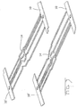
- Figure 1 illustrates at the left a pair of carrier strips 10, 10' with four individual conductors 12 extending therebetween, where the assembly is typically stamped from a sheet metal strip, such as phosphor bronze. Though only one combination has been shown, it will be understood that the carrier strips 10, 10', are continuous or endless with an identical repeat of like conductor arrays or groups arranged therebetween. To the right in Figure 1, the array is shown as viewed from the bottom. In the two views, the various conductors 12 are each provided with a crossover section 14, where the otherwise parallel ends 16 are shifted to different but parallel paths at the opposite end 18. Finally, the carrier strips 10, 10' are provided with registration holes 20. With the respective arrays of Figure 1 arranged to lie contiguous in a back-to-back relationship, and the respective registration holes 20 aligned, the new eight conductor combination array of Figure 2 results.
- the new eight conductor array shows the parallel ends 16, signal entry end, as having a uniform predetermined spacing 22, while the opposite parallel ends 18, the signal exit end, shows a wider or broader, uniform spacing 24.
- the spacings 22 may be 0.040 inches, with spacings 24 at 0.050 inches. With the wider spacings of the exit or outcoming conductors, it was discovered that there is less susceptibility to noise retention at the conductor ends 18.
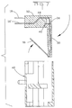
- the array of Figures 2 and 4 is subjected to an insert molding operation, as known in the art.
- the exit ends 18 of the conductors 12 are arranged by separating the conductor ends 18 of four conductors from the carrier strip 10, bending them out of the plane of the remaining conductors, then realigning the free conductor ends 18' in a second plane, parallel to the plane of the remaining conductors, see Figure 5.
- the eight conductor array is subjected to an insert molding operation.
- the respective cross over portion 14 of conductors is fully encapsulated within a plastic insert material 30, having a specified dielectric constant.
- the conductor ends 18, 18' are encapsulated by a second, spaced-apart insert 32.
- the two molded inserts 30, 32 are joined only by the conductor sections 34.
- Figure 7 illustrates, with the aid of the direction arrows, a preferred manner by which the inserts 30, 32 may be arranged to form a unitary insert assembly for housing 40. That is, insert 30 is pivoted 90° about the conductor sections 34, where the projection 42 seats on shoulder 44. Note that the carrier strips 10, 10' have been removed to reveal eight free conductor ends at each end of the assembly. Additionally, the conductor ends 16, or the signal entry ends thereof, are uniformly bent to form plural cantilevered arms, a configuration as known in the art.
- the assembly may be pushed into housing 40 and seated therein as illustrated in Figure 8.
- the resulting connector an external view illustrated in Figure 9, shows the free cantilevered conductor ends 16 resting on a plastic comb 46, as known in the art, while the conductor exit ends 18, 18' extend below the housing 40, to be electrically interconnected to a printed circuit board, not shown, by soldering as practiced in the electronic equipment art, particularly in mounting of electrical connectors to a printed circuit board, where the connectors are preferably top entry or right angle connectors, as known in the art.
- the critical area of crosstalk problems lies with the internal conductor pairs, namely, pairs 4-5 and 3-6.
- the initial data of TABLE III directly compares the NEXT Loss performance of such pairs according to the crossover configuration of U.S. Patent No. 5,186,647 and the present invention. In each case, as the frequency increases, the NEXT Loss in dB drops significantly toward the EIA/TIA minimum standard, of 40.00, at 100 MHz.
- the prior art connector tested just barely meets the minimum, wherein by the use of the unique crossover pattern of the present invention, a nearly 7.00 dB performance improvement is found at a comparable frequency.
- the NEXT Loss performance is generally good for each of the illustrated conductor crossover patterns. However, it is significant to note that for all combinations of pairs, the present invention consistently produced NEXT Loss performance in excess of 45.00, more than 5.00 dB above the minimum requirements for Category 5 products.
- Figures 10 and 11 represent an alternate embodiment to a unique four pair conductor cross over configuration according to this invention.
- the conductors 4 and 5 identified as conductors 54 and 56 respectively, initially cross each other and then each crosses the adjacent 3 or 6 conductor before returning to a parallel and uniformly spaced position.
- the unique conductor cross over configuration of this invention reveals a single cross over of the respective outer pairs, traditionally numbered and identified as pairs 1-2 and 7-8, whereas the inner pairs 3-6 and 4-5, exhibit a situation of at least a double cross over by two of the conductors forming the said inner pairs.
Abstract
Description
- The present invention is directed to electrical connector terminal arrays for electrical connectors, where such arrays offer interference canceling characteristics. The connectors utilizing same are particularly adapted for the telecommunication and electronic industry, where performance requirements have significantly increased to a level identified by industry standards as Category 5. This level of performance is due in large measure to the need for increased data transmission rates requiring improved connecting devices, or hardware.
- The Telecommunications Industry Association (TIA) in cooperation with the Electronic Industries Association (EIA) has developed a proposed standard for Category 5 components, where the transmission requirements of such components are characterized up to 100 MHz and are typically intended for emerging applications with transmission rates up to 100 Mbps. The standard is preliminarily identified as TSB40, August 1992. The invention hereof relates to the hardware, but it is important to note that the hardware is only one major element of a communication system, while another major component is the transmission cable. Thus, it is important to insure the use of the correct connecting component or hardware that is compatible with the transmission characteristics of the cable. Such cables are typically high performance unshielded twisted-pair (UTP) cables, the performance characteristics of which are covered by EIA/TIA bulletin TSB-36.
- Two important test parameters for high performance hardware, i.e. Category 5, are Attenuation and Near-end Cross-Talk (NEXT) Loss where Attenuation may be defined as a measure of signal power loss due to the connecting hardware and is derived from swept frequency voltage measurements on short lengths of 100-ohm twisted pair test leads before and after splicing-in the connector under test. The worst case attenuation of any pair within a connector shall not exceed the values listed below in TABLE I, where for Category 5, the values correspond approximately with attenuation that is equivalent to a 2 meter cable,
TABLE I UTP Connecting Hardware Attenuation Frequency (MHz) Category (dB) 1.0 0.1 4.0 0.1 8.0 0.1 10.0 0.1 16.0 0.2 20.0 0.2 25 0.2 31.25 0.2 62.5 0.3 100 0.4 - Near-end crosstalk loss, the more significant problem, may be defined as a measure of signal coupling from one circuit to another within a connector and is derived from swept frequency voltage measurements on short lengths of 100-ohm twisted-pair test leads terminated to the connector under test. A balanced input signal is applied to a disturbing pair of the connector while the induced signal on the disturbed pair is measured at the near-end of the test leads. In other words, NEXT loss is the way of describing the effects of signal coupling causing portions of the signal on one pair to appear on another pair as unwanted noise. This will become more clear in a description of the test data which appears in TABLE III. In any case, the worst case NEXT loss, see values below in TABLE II, for any combination of disturbing and disturbed pairs is determined by the formula:
- NEXT (F) ≧ NEXT (16) - 20 Log (F/16) where NEXT (16) is the minimum NEXT loss at 16 MHz, F is frequency (in MHz) in the range from 1 MHz to the highest referenced frequency, and NEXT (F) is the performance at that frequency.
TABLE II UTP Connecting Hardware NEXT Loss Limits As specified in EIA/TIA Document TSB-40 Frequency (MHz) Category 5 (dB) 1.0 >65 4.0 >65 8.0 62 10.0 60 16.0 56 20.0 54 25 52 31.25 50 62.5 44 100 40 - U.S. Patent No. 5,186,647 represents a recent development in the disclosure of an electrical connector for conducting high frequency signals, where a major objective thereof is to reduce crosstalk between specific conductors in the connector. A preferred embodiment thereof is a panel mount modular jack which includes a pair of lead frames, each comprising four, flat elongated conductors. The lead frames are mounted on top of each other and their conductors are all generally parallel and close to each other. Only three of the conductors of each lead frame are arranged to overlap each other; and this occurs in a designated crossover region without electrical contact being made because of a reentrant bend in the conductors in the crossover region. As viewed in the assembled condition, the respective conductors within pairs 1-2, 4-5, and 7-8 overlap, while
conductors 3 and 6 are free of any conductor overlap. - With the present invention, it was discovered that a more complex arrangement, involving all conductors, was needed to achieve consistently high performance. It was further discovered that the terminal arrays hereof exhibited reduced noise caused by inductive and capacitive coupling between adjacent signal paths in electrical conductors. Additionally, the arrays according to this invention, with their unique manner of crossing conductors, also reduce the electrical interference coupled to and from nearby circuits caused by electrical signals passing through conductors and terminals. These features will become apparent in the description and data which follow, particularly when read in conjunction with the accompanying drawings.
- This invention is directed to electrical connector terminal arrays, particularly suited for producing jack receptacle type connectors for mounting to a printed circuit board. The connector comprises a dielectric housing into which are mounted, after encapsulation within a molded insert, two terminal arrays that provide four pairs of electrical conductors, where the conductors are arranged essentially in parallel fashion. The respective one ends of the conductors, such as the signal entry ends, are spaced apart a first uniform distance, while the other respective ends thereof are spaced apart a second uniform distance greater than said first uniform distance. The conductors are further characterized by being arranged in a non-contact overlapping arrangement with the respective conductors of each outer pair in a single overlap of each other, and the respective conductors of the center pair crossing each other and then each crossing the adjacent conductor twice. By this arrangement of conductors, the inner pairs of the conductors exhibit a NEXT Loss of at least 45.00 dB at 100 MHz, a value well above that which is necessary to satisfy Category 5 performance requirements.
- Electrical connector terminal arrays comprising a plurality of metal conductors specifically configured to enhance high frequency transmisssion performance through reduction of inductive and capacitive coupling and voltage imbalance between selected conductor pairs, the conductors arranged essentially in a parallel fashion where the respective one ends thereof are spaced apart a first uniform distance, and the other respective ends thereof are spaced apart a second uniform distance greater than the first distance, wherein a central portion is arranged in a non-contact overlapping arrangement with the respective conductors of each outer pair in a single crossover o each other, and the respective conductors of the center pair initially crossing and then continuing outward to cross the adjacent conductors twice, whereby the entire array is insert molded in plastic material having a selected specified dielectric constant.
- The invention will now be described by way of example with reference to the accompanying drawings in which:
- FIGURE 1 illustrates a top and bottom view of a pair of carrier strips including plural conductors therebetween, which when arranged in back-to-back fashion form the initial preferred conductor array crossover configuration according to this invention.
- FIGURE 2 is a top view showing the two carrier strips with conductors of Figure 1 in the initial back-to-back relationship forming the unique four pair configuration.
- FIGURE 3 is a perspective view of the carrier strips with conductors of Figure 1.
- FIGURE 4 is a perspective view of the carrier strips with the four pair crossover configuration of Figure 2.
- FIGURE 5 is a sectional view of the pair of carrier strips with conductors of Figure 4 that have been insert molded prior to forming and inserting into a dielectric housing assembly.
- FIGURE 6 is a side view of the insert molded assembly of Figure 5.
- FIGURE 7 is a sectional view of the formed insert molded assembly just prior to its insertion into a dielectric plug receiving housing assembly.
- FIGURE 8 is a sectional view of the dielectric plug receiving housing with insert mounted therein.
- FIGURE 9 is a perspective view of the assembly of Figure 8, as may be constructed in accordance with this invention.
- FIGURE 10 illustrates a top and bottom view of an alternate embodiment to the array configuration of Figure 1.
- FIGURE 11 is a top view, similar to Figure 2, showing the alternate four pair configuration of the conductors of Figure 10 in the initial back-to-back relationship.
- The present invention is directed to electrical conductor terminal arrays which, by their unique conductor configuration, offer reduced electrical noise caused by inductive and capacitive coupling and voltage imbalance between adjacent signal paths in electrical connectors intended for the telecommunication industry. Connectors, typically of the plug and jack receptacle type, are controlled by FCC regulations to ensure compatibility between equipment from various manufacturers. Unfortunately, however, the conductor pair assignments specified in EIA/TIA 56B standard are not optimum for meeting the Category 5 requirement of low Near End Crosstalk which is the description used to describe the effects of unwanted signal coupling causing portions of the signal on one pair to appear on another pair as unwanted noise. Typical standard RJ45 connectors have approximately 100 MHz crosstalk loss of 28 dB on the 4-5 → 3-6 pairs, the critical internal pairs of an eight conductor assembly. By way of further reference and understanding, as viewed from the top of a planar arrangement of conductors, such conductors are numbered consecutively from 1 to 8, left to right. Additionally, such conductors exhibit alternating polarity from "1 positive" to "8 negative".
- With this understanding, reference may now be made to the several Figures, where Figures 1-4 represent the preferred embodiment of developing the unique arrangement or crossover pattern of conductors. Figure 1 illustrates at the left a pair of
carrier strips individual conductors 12 extending therebetween, where the assembly is typically stamped from a sheet metal strip, such as phosphor bronze. Though only one combination has been shown, it will be understood that thecarrier strips various conductors 12 are each provided with acrossover section 14, where the otherwiseparallel ends 16 are shifted to different but parallel paths at theopposite end 18. Finally, thecarrier strips registration holes 20. With the respective arrays of Figure 1 arranged to lie contiguous in a back-to-back relationship, and therespective registration holes 20 aligned, the new eight conductor combination array of Figure 2 results. - In order to avoid conductor contact in the
crossover section 14, the path of the conductor is changed, see Figures 3 and 4. In a right-handed coordinate system, where the plane of thecarrier strips 10 and array ofconductors 12 of Figure 1 define the X-Y plane, and the Z direction is orthonormal thereto, the conductors are shifted not only in the X-Y plane, but in the Z direction. By suitably bending the conductors, in the manner illustrated, contact during crossover is avoided and the cancellation characteristics are enhanced. A preferred, uniform crossover spacing is .018 inches. - As best seen by the illustration of Figure 2, the new eight conductor array shows the
parallel ends 16, signal entry end, as having a uniformpredetermined spacing 22, while the opposite parallel ends 18, the signal exit end, shows a wider or broader,uniform spacing 24. In a preferred embodiment thespacings 22 may be 0.040 inches, withspacings 24 at 0.050 inches. With the wider spacings of the exit or outcoming conductors, it was discovered that there is less susceptibility to noise retention at the conductor ends 18. - Returning to the cross-over pattern in the array of conductors of Figure 2, it will be seen that all conductors are subjected to a crossover from at least one other conductor. In the respective outer pairs, namely pairs 1-2 and 7-8, there is just a single angled crossover within the
section 14. However, the crossover patterns of the inner conductors 3-4-5-6 are significantly different. Conductors 4 and 5 cross each other and then each crosses the adjacent 3 or 6 conductor twice. As will be demonstrated in the data and description which follows, the inner conductors 3-4-5-6, specifically the pairs 4-5 and 3-6, are the critical areas for the worst cross talk problems. - In preparing the conductor array for inclusion in a suitable connector housing, the array of Figures 2 and 4 is subjected to an insert molding operation, as known in the art. The exit ends 18 of the
conductors 12 are arranged by separating the conductor ends 18 of four conductors from thecarrier strip 10, bending them out of the plane of the remaining conductors, then realigning the free conductor ends 18' in a second plane, parallel to the plane of the remaining conductors, see Figure 5. - In this arrangement, with the use of spacers, as known in the molding art, to ensure precise spacing, preferably .018 inches, in the cross over
portion 14, the eight conductor array is subjected to an insert molding operation. Specifically, the respective cross overportion 14 of conductors is fully encapsulated within aplastic insert material 30, having a specified dielectric constant. Concurrently, the conductor ends 18, 18' are encapsulated by a second, spaced-apartinsert 32. As seen in Figures 5 and 6, the two moldedinserts conductor sections 34. - Figure 7 illustrates, with the aid of the direction arrows, a preferred manner by which the
inserts housing 40. That is,insert 30 is pivoted 90° about theconductor sections 34, where theprojection 42 seats onshoulder 44. Note that the carrier strips 10, 10' have been removed to reveal eight free conductor ends at each end of the assembly. Additionally, the conductor ends 16, or the signal entry ends thereof, are uniformly bent to form plural cantilevered arms, a configuration as known in the art. - With the
insert assembly housing 40 and seated therein as illustrated in Figure 8. The resulting connector, an external view illustrated in Figure 9, shows the free cantilevered conductor ends 16 resting on aplastic comb 46, as known in the art, while the conductor exit ends 18, 18' extend below thehousing 40, to be electrically interconnected to a printed circuit board, not shown, by soldering as practiced in the electronic equipment art, particularly in mounting of electrical connectors to a printed circuit board, where the connectors are preferably top entry or right angle connectors, as known in the art. - Having described the assembly and conductor configuration of this invention, a series of comparative tests were conducted using the conductor array configuration of present Figure 2, and a conductor configuration according to the prior art, as exemplified by Fig. 10 of U.S. Patent No. 5,186,647. The series of tests included monitoring the induced signal of each designated pair of conductors from another pair. The results thereof are presented below in TABLE III.


- The critical area of crosstalk problems lies with the internal conductor pairs, namely, pairs 4-5 and 3-6. The initial data of TABLE III directly compares the NEXT Loss performance of such pairs according to the crossover configuration of U.S. Patent No. 5,186,647 and the present invention. In each case, as the frequency increases, the NEXT Loss in dB drops significantly toward the EIA/TIA minimum standard, of 40.00, at 100 MHz. The prior art connector tested just barely meets the minimum, wherein by the use of the unique crossover pattern of the present invention, a nearly 7.00 dB performance improvement is found at a comparable frequency.
- Outside the area of such critical pairs, the NEXT Loss performance is generally good for each of the illustrated conductor crossover patterns. However, it is significant to note that for all combinations of pairs, the present invention consistently produced NEXT Loss performance in excess of 45.00, more than 5.00 dB above the minimum requirements for Category 5 products.
- Figures 10 and 11 represent an alternate embodiment to a unique four pair conductor cross over configuration according to this invention. In this configuration, the conductors 4 and 5, identified as
conductors
Claims (10)
- Electrical connector terminal arrays comprising a plurality of metal conductors (12) specifically configured to enhance high frequency transmission performance through reduction of inductive and capacitive coupling and voltage imbalance between selected conductor pairs, said conductors arranged essentially in a parallel fashion where the respective one ends thereof are spaced apart a first uniform distance, and the other respective ends thereof are spaced apart a second uniform distance greater than said first distance,
characterized by a central portion (14) arranged in a non-contact overlapping arrangement with the respective conductors of each outer pair in a single crossover of each other, and the respective conductors of a center pair initially crossing and then continuing outward to cross the adjacent conductors twice, whereby the entire array is insert molded in plastic material (30, 32) having a selected specified dielectric constant. - The electrical connector terminal arrays of claim 1, wherein said first uniform distance is about 1mm (0.040 inches) and said second uniform distance is about 1.3 mm (0.050 inches).
- The electrical connector terminal arrays of claim 1 or 2, wherein the conductor overlap spacing is a uniform distance of about 0.5 mm (0.018 inches).
- The electrical connector terminal arrays of claim 1, 2 or 3, wherein the insert molding (30) extends throughout the conductor overlapping arrangement from a location where the conductors are parallel along said first uniform distance to a location where said conductors are parallel along said second uniform distance.
- The electrical connector terminal arrays of claim 4 are arranged within a connector housing (40) to produce a printed circuit board mounted top entry and right angle connectors surpassing the requirements of EIA/TIA specification TSB-40.
- Electrical connector terminal arrays comprising four pairs of metal conductors (12) specifically configured to enhance high frequency transmission performance through reduction of voltage imbalance and of inductive and capacitive coupling between selected conductor pairs, said conductors arranged essentially in parallel fashion where the respective one ends thereof are spaced apart a first uniform distance, and the other respective ends thereof are spaced apart a second uniform distance greater than said first distance,
characterized by a central portion (14) arranged in a non-contact overlapping arrangement with the respective conductors of each outer pair in a single crossover of each other, and the inner two pairs arranged such that at least two conductors thereof crossover two other of said inner conductors, whereby the entire array is insert molded in plastic material (30, 32) having a selected specified dielectric constant. - The electrical connector terminal arrays of claim 6, wherein said first uniform distance is about 1mm (0.040 inches) and said second uniform distance is about 1.3 mm (0.050 inches).
- The electrical connector terminal arrays of claim 6, wherein the conductor overlap spacing is a uniform distance of about 0.5 mm (0.018 inches)
- The electrical connector terminal arrays of claim 6, 7 or 8, wherein the insert molding (30) extends throughout the conductor overlapping arrangement from a location where the conductors are parallel along said first uniform distance to a location where said conductors are parallel along said second uniform distance.
- The electrical connector terminal arrays of claim 9 being mounted on a printed circuit board assembly to produce panel mount connectors surpassing the requirements of EIA/TIA specification TSB-40.
Applications Claiming Priority (2)
| Application Number | Priority Date | Filing Date | Title |
|---|---|---|---|
| US88934 | 1993-07-08 | ||
| US08/088,934 US5362257A (en) | 1993-07-08 | 1993-07-08 | Communications connector terminal arrays having noise cancelling capabilities |
Publications (3)
| Publication Number | Publication Date |
|---|---|
| EP0633632A2 true EP0633632A2 (en) | 1995-01-11 |
| EP0633632A3 EP0633632A3 (en) | 1996-07-03 |
| EP0633632B1 EP0633632B1 (en) | 2000-04-05 |
Family
ID=22214378
Family Applications (1)
| Application Number | Title | Priority Date | Filing Date |
|---|---|---|---|
| EP94110605A Expired - Lifetime EP0633632B1 (en) | 1993-07-08 | 1994-07-07 | Communications connector terminal arrays having noise cancelling capabilities |
Country Status (10)
| Country | Link |
|---|---|
| US (1) | US5362257A (en) |
| EP (1) | EP0633632B1 (en) |
| JP (1) | JP3400123B2 (en) |
| KR (1) | KR100340693B1 (en) |
| CN (1) | CN1044761C (en) |
| AU (1) | AU673061B2 (en) |
| BR (1) | BR9402637A (en) |
| CA (1) | CA2123260C (en) |
| DE (1) | DE69423824D1 (en) |
| TW (1) | TW224547B (en) |
Cited By (1)
| Publication number | Priority date | Publication date | Assignee | Title |
|---|---|---|---|---|
| DE19938367C2 (en) * | 1999-08-13 | 2002-09-26 | Gaertner Karl Telegaertner | Modular socket |
Families Citing this family (119)
| Publication number | Priority date | Publication date | Assignee | Title |
|---|---|---|---|---|
| GB2271678B (en) * | 1993-12-03 | 1994-10-12 | Itt Ind Ltd | Electrical connector |
| DE69421798T2 (en) * | 1994-03-26 | 2004-07-15 | Molex Inc., Lisle | Modular Jack connector |
| DE69430194T2 (en) * | 1994-07-14 | 2002-10-31 | Molex Inc | Modular connector with reduced crosstalk |
| US5593317A (en) * | 1994-08-31 | 1997-01-14 | The Whitaker Corporation | Modular furniture communication system |
| EP0709930A3 (en) | 1994-10-28 | 1997-09-10 | Whitaker Corp | Capacitive trace coupling for reduction of crosstalk |
| US5488201A (en) * | 1994-12-16 | 1996-01-30 | Dan-Chief Enterprise Co., Ltd. | Low crosstalk electrical signal transmission medium |
| US5647767A (en) * | 1995-02-06 | 1997-07-15 | The Whitaker Corporation | Electrical connector jack assembly for signal transmission |
| US5587884A (en) * | 1995-02-06 | 1996-12-24 | The Whitaker Corporation | Electrical connector jack with encapsulated signal conditioning components |
| GB9509886D0 (en) * | 1995-05-16 | 1995-07-12 | Amp Holland | Modular plug for high speed data transmission |
| FR2734418A1 (en) * | 1995-05-16 | 1996-11-22 | Amp France | CONNECTOR, ESPECIALLY OF THE MODULAR JACK TYPE |
| US5586914A (en) * | 1995-05-19 | 1996-12-24 | The Whitaker Corporation | Electrical connector and an associated method for compensating for crosstalk between a plurality of conductors |
| US5791943A (en) * | 1995-11-22 | 1998-08-11 | The Siemon Company | Reduced crosstalk modular outlet |
| AU716436B2 (en) * | 1995-12-25 | 2000-02-24 | Matsushita Electric Works Ltd. | Connector |
| US5647770A (en) * | 1995-12-29 | 1997-07-15 | Berg Technology, Inc. | Insert for a modular jack useful for reducing electrical crosstalk |
| US5879199A (en) * | 1996-02-29 | 1999-03-09 | Berg Technology, Inc. | Modular jack assembly and universal housing for use therein |
| US6065994A (en) * | 1996-06-21 | 2000-05-23 | Lucent Technologies Inc. | Low-crosstalk electrical connector grouping like conductors together |
| US5911602A (en) * | 1996-07-23 | 1999-06-15 | Superior Modular Products Incorporated | Reduced cross talk electrical connector |
| US6050842A (en) * | 1996-09-27 | 2000-04-18 | The Whitaker Corporation | Electrical connector with paired terminals |
| US5779503A (en) * | 1996-12-18 | 1998-07-14 | Nordx/Cdt, Inc. | High frequency connector with noise cancelling characteristics |
| JP3528484B2 (en) * | 1996-12-27 | 2004-05-17 | モレックス インコーポレーテッド | Pseudo twisted pair flat flexible cable |
| US5961354A (en) * | 1997-01-13 | 1999-10-05 | Lucent Technologies, Inc. | Electrical connector assembly |
| US5997358A (en) * | 1997-09-02 | 1999-12-07 | Lucent Technologies Inc. | Electrical connector having time-delayed signal compensation |
| CH693012A5 (en) * | 1997-06-02 | 2003-01-15 | Reichle & De Massari Fa | A plug connector for high-frequency data transmission over electrical conductors. |
| US5921818A (en) * | 1997-06-23 | 1999-07-13 | Lucent Technologies Inc. | Low crosstalk electrical connector |
| JP3238895B2 (en) * | 1997-08-28 | 2001-12-17 | ヒロセ電機株式会社 | Modular jack |
| CN1282455A (en) * | 1997-10-09 | 2001-01-31 | 斯图尔特连接器系统公司 | High frequency bi-level offset multi-port jack |
| US6007368A (en) * | 1997-11-18 | 1999-12-28 | Leviton Manufacturing Company, Inc. | Telecommunications connector with improved crosstalk reduction |
| US6000955A (en) * | 1997-12-10 | 1999-12-14 | Gabriel Technologies, Inc. | Multiple terminal edge connector |
| US6162089A (en) * | 1997-12-30 | 2000-12-19 | The Whitaker Corporation | Stacked LAN connector |
| US5971813A (en) * | 1998-04-01 | 1999-10-26 | Regal Electronics, Inc. | RJ-45 modular connector with microwave-transmission-line integrated signal conditioning for high speed networks |
| US6171152B1 (en) | 1998-04-01 | 2001-01-09 | Regal Electronics, Inc. | Standard footprint and form factor RJ-45 connector with integrated signal conditioning for high speed networks |
| US6120329A (en) * | 1998-05-08 | 2000-09-19 | The Whitaker Corporation | Modular jack with anti-cross-talk contacts and method of making same |
| DE19822630C1 (en) * | 1998-05-20 | 2000-09-07 | Krone Gmbh | Arrangement of contact pairs to compensate for the near crosstalk for an electrical connector |
| AU755916B2 (en) | 1998-06-02 | 2003-01-02 | Stewart Connector Systems, Inc. | High frequency electrical connector assembly such as a multi-port multi-level connector assembly |
| US6300687B1 (en) * | 1998-06-26 | 2001-10-09 | International Business Machines Corporation | Micro-flex technology in semiconductor packages |
| US6066005A (en) * | 1998-06-30 | 2000-05-23 | Berg Technology, Inc. | Vertical modular connector having low electrical crosstalk |
| US6033266A (en) * | 1998-08-31 | 2000-03-07 | The Whitaker Corporation | Modular connector with preload and beam length reduction features |
| JP3333457B2 (en) * | 1998-10-16 | 2002-10-15 | ヒロセ電機株式会社 | Modular connector |
| US6394822B1 (en) * | 1998-11-24 | 2002-05-28 | Teradyne, Inc. | Electrical connector |
| US6152747A (en) * | 1998-11-24 | 2000-11-28 | Teradyne, Inc. | Electrical connector |
| HUP0105197A2 (en) * | 1999-01-15 | 2002-05-29 | Adc Telecommunications Inc | Telecommunications jack assembly |
| US6334792B1 (en) | 1999-01-15 | 2002-01-01 | Adc Telecommunications, Inc. | Connector including reduced crosstalk spring insert |
| US6394835B1 (en) | 1999-02-16 | 2002-05-28 | Hubbell Incorporated | Wiring unit with paired in-line insulation displacement contacts |
| US6186834B1 (en) * | 1999-06-08 | 2001-02-13 | Avaya Technology Corp. | Enhanced communication connector assembly with crosstalk compensation |
| US6520806B2 (en) | 1999-08-20 | 2003-02-18 | Adc Telecommunications, Inc. | Telecommunications connector for high frequency transmissions |
| US6089923A (en) | 1999-08-20 | 2000-07-18 | Adc Telecommunications, Inc. | Jack including crosstalk compensation for printed circuit board |
| US6962503B2 (en) | 2000-01-10 | 2005-11-08 | Ortronics, Inc. | Unshielded twisted pair (UTP) wire stabilizer for communication plug |
| US6193560B1 (en) | 2000-03-03 | 2001-02-27 | Tyco Electronics Corporation | Connector assembly with side-by-side terminal arrays |
| US6533618B1 (en) | 2000-03-31 | 2003-03-18 | Ortronics, Inc. | Bi-directional balance low noise communication interface |
| US6270381B1 (en) * | 2000-07-07 | 2001-08-07 | Avaya Technology Corp. | Crosstalk compensation for electrical connectors |
| US6331126B1 (en) | 2000-09-07 | 2001-12-18 | Sentinel Holding, Inc. | High speed modular jack |
| GB2367194A (en) * | 2000-09-15 | 2002-03-27 | R W Data Ltd | Socket for data transmission. |
| US6802743B2 (en) | 2000-09-29 | 2004-10-12 | Ortronics, Inc. | Low noise communication modular connector insert |
| US6729901B2 (en) | 2000-09-29 | 2004-05-04 | Ortronics, Inc. | Wire guide sled hardware for communication plug |
| US6486405B2 (en) * | 2000-12-01 | 2002-11-26 | Hon Hai Precision Ind. Co., Ltd. | Arrangement of differential pair for eliminating crosstalk in high speed application |
| US6585540B2 (en) | 2000-12-06 | 2003-07-01 | Pulse Engineering | Shielded microelectronic connector assembly and method of manufacturing |
| US6896557B2 (en) * | 2001-03-28 | 2005-05-24 | Ortronics, Inc. | Dual reactance low noise modular connector insert |
| US7172466B2 (en) * | 2001-04-05 | 2007-02-06 | Ortronics, Inc. | Dual reactance low noise modular connector insert |
| US6744329B2 (en) * | 2001-12-14 | 2004-06-01 | Yazaki North America, Inc. | Cross talk compensation circuit |
| DE10211603C1 (en) * | 2002-03-12 | 2003-10-02 | Ackermann Albert Gmbh Co | Electrical connector for data technology |
| DE10242143A1 (en) * | 2002-09-04 | 2004-03-25 | Telegärtner Karl Gärtner GmbH | Electrical socket |
| US6688909B1 (en) | 2002-10-03 | 2004-02-10 | Hon Hai Precision Ind. Co., Ltd. | Stacked connector with leds |
| US6638121B1 (en) | 2002-10-04 | 2003-10-28 | Hon Hai Precision Ind. Co., Ltd. | Stacked connector with LEDs and method of producing the same |
| US6796847B2 (en) | 2002-10-21 | 2004-09-28 | Hubbell Incorporated | Electrical connector for telecommunications applications |
| US6682365B1 (en) | 2002-11-05 | 2004-01-27 | Hon Hai Precision Ind. Co., Ltd. | Stacked connector with plastic part assembled thereto |
| US6964587B2 (en) * | 2002-11-10 | 2005-11-15 | Bel Fuse Ltd. | High performance, high capacitance gain, jack connector for data transmission or the like |
| US6814624B2 (en) * | 2002-11-22 | 2004-11-09 | Adc Telecommunications, Inc. | Telecommunications jack assembly |
| US7489219B2 (en) * | 2003-07-16 | 2009-02-10 | Marvell World Trade Ltd. | Power inductor with reduced DC current saturation |
| US7023313B2 (en) * | 2003-07-16 | 2006-04-04 | Marvell World Trade Ltd. | Power inductor with reduced DC current saturation |
| US7307502B2 (en) * | 2003-07-16 | 2007-12-11 | Marvell World Trade Ltd. | Power inductor with reduced DC current saturation |
| JP4292983B2 (en) * | 2003-12-24 | 2009-07-08 | 市光工業株式会社 | Motor drive device and electric retractable door mirror |
| US6916209B1 (en) | 2004-01-23 | 2005-07-12 | Molex Incorporated | Electrical signal transmission system |
| US8324872B2 (en) | 2004-03-26 | 2012-12-04 | Marvell World Trade, Ltd. | Voltage regulator with coupled inductors having high coefficient of coupling |
| US7153168B2 (en) * | 2004-04-06 | 2006-12-26 | Panduit Corp. | Electrical connector with improved crosstalk compensation |
| CA2464834A1 (en) | 2004-04-19 | 2005-10-19 | Nordx/Cdt Inc. | Connector |
| US7241181B2 (en) | 2004-06-29 | 2007-07-10 | Pulse Engineering, Inc. | Universal connector assembly and method of manufacturing |
| US7264516B2 (en) * | 2004-12-06 | 2007-09-04 | Commscope, Inc. | Communications jack with printed wiring board having paired coupling conductors |
| US7168993B2 (en) * | 2004-12-06 | 2007-01-30 | Commscope Solutions Properties Llc | Communications connector with floating wiring board for imparting crosstalk compensation between conductors |
| US7326089B2 (en) * | 2004-12-07 | 2008-02-05 | Commscope, Inc. Of North Carolina | Communications jack with printed wiring board having self-coupling conductors |
| US7186149B2 (en) * | 2004-12-06 | 2007-03-06 | Commscope Solutions Properties, Llc | Communications connector for imparting enhanced crosstalk compensation between conductors |
| US7186148B2 (en) * | 2004-12-07 | 2007-03-06 | Commscope Solutions Properties, Llc | Communications connector for imparting crosstalk compensation between conductors |
| US7220149B2 (en) * | 2004-12-07 | 2007-05-22 | Commscope Solutions Properties, Llc | Communication plug with balanced wiring to reduce differential to common mode crosstalk |
| US7204722B2 (en) * | 2004-12-07 | 2007-04-17 | Commscope Solutions Properties, Llc | Communications jack with compensation for differential to differential and differential to common mode crosstalk |
| US7166000B2 (en) * | 2004-12-07 | 2007-01-23 | Commscope Solutions Properties, Llc | Communications connector with leadframe contact wires that compensate differential to common mode crosstalk |
| ATE505852T1 (en) * | 2004-12-07 | 2011-04-15 | Commscope Inc | COMMUNICATION PLUG WITH COMPENSATION OF DIFFERENTIAL TO DIFFERENTIAL AND DIFFERENTIAL TO COMMON CROSSTALK |
| US7320624B2 (en) * | 2004-12-16 | 2008-01-22 | Commscope, Inc. Of North Carolina | Communications jacks with compensation for differential to differential and differential to common mode crosstalk |
| WO2006081423A1 (en) | 2005-01-28 | 2006-08-03 | Commscope Inc. Of North Carolina | Controlled mode conversion connector for reduced alien crosstalk |
| US7314393B2 (en) | 2005-05-27 | 2008-01-01 | Commscope, Inc. Of North Carolina | Communications connectors with floating wiring board for imparting crosstalk compensation between conductors |
| CN101087050B (en) * | 2006-06-06 | 2010-10-06 | 富士康(昆山)电脑接插件有限公司 | Module connector |
| US7530854B2 (en) * | 2006-06-15 | 2009-05-12 | Ortronics, Inc. | Low noise multiport connector |
| US7364470B2 (en) * | 2006-07-05 | 2008-04-29 | Commscope, Inc. Of North Carolina | Communications connectors with signal current splitting |
| US7288001B1 (en) | 2006-09-20 | 2007-10-30 | Ortronics, Inc. | Electrically isolated shielded multiport connector assembly |
| US7485010B2 (en) * | 2007-06-14 | 2009-02-03 | Ortronics, Inc. | Modular connector exhibiting quad reactance balance functionality |
| USD612856S1 (en) | 2008-02-20 | 2010-03-30 | Vocollect Healthcare Systems, Inc. | Connector for a peripheral device |
| US7722406B2 (en) * | 2008-03-17 | 2010-05-25 | Zippy Technology Corp. | Output adapting device of plug-in power system |
| DE102008022610A1 (en) * | 2008-05-08 | 2009-11-12 | Krones Ag | Electrical plug connection |
| US7914345B2 (en) * | 2008-08-13 | 2011-03-29 | Tyco Electronics Corporation | Electrical connector with improved compensation |
| DE102008064535A1 (en) | 2008-12-19 | 2010-06-24 | Telegärtner Karl Gärtner GmbH | Electrical connector |
| US8425261B2 (en) | 2009-03-02 | 2013-04-23 | Tyco Electronics Corporation | Electrical connector with contact spacing member |
| US7927152B2 (en) | 2009-03-02 | 2011-04-19 | Tyco Electronics Corporation | Electrical connector with contact spacing member |
| USD615040S1 (en) | 2009-09-09 | 2010-05-04 | Vocollect, Inc. | Electrical connector |
| US8241053B2 (en) * | 2009-09-10 | 2012-08-14 | Vocollect, Inc. | Electrical cable with strength member |
| US8262403B2 (en) * | 2009-09-10 | 2012-09-11 | Vocollect, Inc. | Break-away electrical connector |
| US7909656B1 (en) * | 2009-10-26 | 2011-03-22 | Leviton Manufacturing Co., Inc. | High speed data communications connector with reduced modal conversion |
| JP5595289B2 (en) * | 2011-01-06 | 2014-09-24 | 富士通コンポーネント株式会社 | connector |
| JP5090554B2 (en) * | 2011-04-04 | 2012-12-05 | 日本航空電子工業株式会社 | Connector member |
| CN103947055B (en) | 2011-11-23 | 2017-03-08 | 泛达公司 | Compensation network using quadrature compensation network |
| US9136647B2 (en) | 2012-06-01 | 2015-09-15 | Panduit Corp. | Communication connector with crosstalk compensation |
| EP3761458A1 (en) | 2012-07-16 | 2021-01-06 | CommScope, Inc. of North Carolina | Balanced pin and socket connectors |
| US9246463B2 (en) | 2013-03-07 | 2016-01-26 | Panduit Corp. | Compensation networks and communication connectors using said compensation networks |
| US9257792B2 (en) | 2013-03-14 | 2016-02-09 | Panduit Corp. | Connectors and systems having improved crosstalk performance |
| US9590339B2 (en) | 2013-05-09 | 2017-03-07 | Commscope, Inc. Of North Carolina | High data rate connectors and cable assemblies that are suitable for harsh environments and related methods and systems |
| JP5669285B1 (en) * | 2014-02-21 | 2015-02-12 | 日本航空電子工業株式会社 | connector |
| DE102014104446A1 (en) | 2014-03-28 | 2015-10-01 | Telegärtner Karl Gärtner GmbH | Electrical connector |
| DE102014104449A1 (en) | 2014-03-28 | 2015-10-01 | Telegärtner Karl Gärtner GmbH | Electrical connector |
| JP6452512B2 (en) * | 2015-03-18 | 2019-01-16 | 日本航空電子工業株式会社 | connector |
| US9634433B1 (en) * | 2016-04-13 | 2017-04-25 | Panduit Corp. | Communication jack having a dielectric film between plug interface contacts |
| TWI595708B (en) * | 2017-01-06 | 2017-08-11 | 慶陞工業股份有限公司 | Modular connector |
| JP7109353B2 (en) * | 2018-12-12 | 2022-07-29 | 日本航空電子工業株式会社 | modular jack |
Citations (4)
| Publication number | Priority date | Publication date | Assignee | Title |
|---|---|---|---|---|
| US3757028A (en) * | 1972-09-18 | 1973-09-04 | J Schlessel | Terference printed board and similar transmission line structure for reducing in |
| DE8901012U1 (en) * | 1988-02-02 | 1989-03-09 | Amp Inc., Harrisburg, Pa., Us | |
| EP0337632A1 (en) * | 1988-04-11 | 1989-10-18 | The Whitaker Corporation | Electrical device having improved leads for surface mounting on a circuit board |
| US5186647A (en) * | 1992-02-24 | 1993-02-16 | At&T Bell Laboratories | High frequency electrical connector |
Family Cites Families (3)
| Publication number | Priority date | Publication date | Assignee | Title |
|---|---|---|---|---|
| JPH03196477A (en) * | 1989-12-26 | 1991-08-27 | Hirose Electric Co Ltd | Modular jack and method for expanding pitch of jack terminal |
| US5282754A (en) * | 1992-09-03 | 1994-02-01 | Northern Telecom Limited | Multi-terminal electrical connectors |
| US5269708A (en) * | 1993-03-03 | 1993-12-14 | Adc Telecommunications, Inc. | Patch panel for high speed twisted pair |
-
1993
- 1993-07-08 US US08/088,934 patent/US5362257A/en not_active Expired - Lifetime
- 1993-12-17 TW TW082110692A patent/TW224547B/en not_active IP Right Cessation
-
1994
- 1994-05-10 CA CA002123260A patent/CA2123260C/en not_active Expired - Lifetime
- 1994-05-13 AU AU63088/94A patent/AU673061B2/en not_active Expired
- 1994-07-05 KR KR1019940015966A patent/KR100340693B1/en not_active IP Right Cessation
- 1994-07-05 BR BR9402637A patent/BR9402637A/en not_active Application Discontinuation
- 1994-07-06 CN CN94108188A patent/CN1044761C/en not_active Expired - Fee Related
- 1994-07-07 DE DE69423824T patent/DE69423824D1/en not_active Expired - Lifetime
- 1994-07-07 EP EP94110605A patent/EP0633632B1/en not_active Expired - Lifetime
- 1994-07-08 JP JP18090394A patent/JP3400123B2/en not_active Expired - Lifetime
Patent Citations (4)
| Publication number | Priority date | Publication date | Assignee | Title |
|---|---|---|---|---|
| US3757028A (en) * | 1972-09-18 | 1973-09-04 | J Schlessel | Terference printed board and similar transmission line structure for reducing in |
| DE8901012U1 (en) * | 1988-02-02 | 1989-03-09 | Amp Inc., Harrisburg, Pa., Us | |
| EP0337632A1 (en) * | 1988-04-11 | 1989-10-18 | The Whitaker Corporation | Electrical device having improved leads for surface mounting on a circuit board |
| US5186647A (en) * | 1992-02-24 | 1993-02-16 | At&T Bell Laboratories | High frequency electrical connector |
Cited By (1)
| Publication number | Priority date | Publication date | Assignee | Title |
|---|---|---|---|---|
| DE19938367C2 (en) * | 1999-08-13 | 2002-09-26 | Gaertner Karl Telegaertner | Modular socket |
Also Published As
| Publication number | Publication date |
|---|---|
| KR950004642A (en) | 1995-02-18 |
| DE69423824D1 (en) | 2000-05-11 |
| JP3400123B2 (en) | 2003-04-28 |
| JPH07106010A (en) | 1995-04-21 |
| US5362257A (en) | 1994-11-08 |
| BR9402637A (en) | 1995-04-04 |
| AU673061B2 (en) | 1996-10-24 |
| KR100340693B1 (en) | 2002-11-18 |
| AU6308894A (en) | 1995-01-19 |
| CN1100879A (en) | 1995-03-29 |
| CA2123260A1 (en) | 1995-01-09 |
| CN1044761C (en) | 1999-08-18 |
| EP0633632A3 (en) | 1996-07-03 |
| EP0633632B1 (en) | 2000-04-05 |
| CA2123260C (en) | 2004-09-14 |
| TW224547B (en) | 1994-06-01 |
Similar Documents
| Publication | Publication Date | Title |
|---|---|---|
| EP0633632B1 (en) | Communications connector terminal arrays having noise cancelling capabilities | |
| AU739904B2 (en) | Crosstalk compensation for connector jack | |
| CA2225108C (en) | High frequency connector with noise cancelling characteristics | |
| US6592395B2 (en) | In-line cable connector assembly | |
| EP1059704B1 (en) | Communication connector assembly with crosstalk compensation | |
| US5575680A (en) | Insulation displacement connector and block | |
| US7140924B2 (en) | Compensation system and method for negative capacitive coupling in IDC | |
| EP1160935B1 (en) | Communication connector with crosstalk compensation | |
| US20180123293A1 (en) | Electrical jack with a plurality of parallel and overlapping capacitive plates | |
| US8007311B2 (en) | Electrical connector | |
| US8133069B2 (en) | Electrical connector | |
| EP0856919A2 (en) | Low crosstalk noise connector for telecommunication systems | |
| EP0668634A2 (en) | High performance electrical connector | |
| US6165018A (en) | Connector having internal crosstalk compensation | |
| US5399106A (en) | High performance electrical connector | |
| WO1999019944A1 (en) | High frequency bi-level offset multi-port jack | |
| US20100167577A1 (en) | Electrical connector | |
| US8272888B2 (en) | Electrical connector | |
| US7474737B2 (en) | Telecommunications test plugs having tuned near end crosstalk | |
| EP1255322B1 (en) | Crosstalk reduction for IDC terminal block | |
| EP0993081A2 (en) | Modular connector with capacitive plates |
Legal Events
| Date | Code | Title | Description |
|---|---|---|---|
| PUAI | Public reference made under article 153(3) epc to a published international application that has entered the european phase |
Free format text: ORIGINAL CODE: 0009012 |
|
| AK | Designated contracting states |
Kind code of ref document: A2 Designated state(s): CH DE ES FR GB IT LI NL SE |
|
| PUAL | Search report despatched |
Free format text: ORIGINAL CODE: 0009013 |
|
| AK | Designated contracting states |
Kind code of ref document: A3 Designated state(s): CH DE ES FR GB IT LI NL SE |
|
| 17P | Request for examination filed |
Effective date: 19961218 |
|
| GRAG | Despatch of communication of intention to grant |
Free format text: ORIGINAL CODE: EPIDOS AGRA |
|
| 17Q | First examination report despatched |
Effective date: 19990505 |
|
| GRAG | Despatch of communication of intention to grant |
Free format text: ORIGINAL CODE: EPIDOS AGRA |
|
| GRAH | Despatch of communication of intention to grant a patent |
Free format text: ORIGINAL CODE: EPIDOS IGRA |
|
| GRAH | Despatch of communication of intention to grant a patent |
Free format text: ORIGINAL CODE: EPIDOS IGRA |
|
| GRAA | (expected) grant |
Free format text: ORIGINAL CODE: 0009210 |
|
| RIC1 | Information provided on ipc code assigned before grant |
Free format text: 7H 01R 24/00 A, 7H 01R 12/16 B |
|
| AK | Designated contracting states |
Kind code of ref document: B1 Designated state(s): CH DE ES FR GB IT LI NL SE |
|
| PG25 | Lapsed in a contracting state [announced via postgrant information from national office to epo] |
Ref country code: NL Free format text: LAPSE BECAUSE OF FAILURE TO SUBMIT A TRANSLATION OF THE DESCRIPTION OR TO PAY THE FEE WITHIN THE PRESCRIBED TIME-LIMIT Effective date: 20000405 Ref country code: IT Free format text: LAPSE BECAUSE OF FAILURE TO SUBMIT A TRANSLATION OF THE DESCRIPTION OR TO PAY THE FEE WITHIN THE PRE;WARNING: LAPSES OF ITALIAN PATENTS WITH EFFECTIVE DATE BEFORE 2007 MAY HAVE OCCURRED AT ANY TIME BEFORE 2007. THE CORRECT EFFECTIVE DATE MAY BE DIFFERENT FROM THE ONE RECORDED.SCRIBED TIME-LIMIT Effective date: 20000405 Ref country code: FR Free format text: LAPSE BECAUSE OF FAILURE TO SUBMIT A TRANSLATION OF THE DESCRIPTION OR TO PAY THE FEE WITHIN THE PRESCRIBED TIME-LIMIT Effective date: 20000405 Ref country code: ES Free format text: THE PATENT HAS BEEN ANNULLED BY A DECISION OF A NATIONAL AUTHORITY Effective date: 20000405 |
|
| REG | Reference to a national code |
Ref country code: CH Ref legal event code: EP |
|
| REF | Corresponds to: |
Ref document number: 69423824 Country of ref document: DE Date of ref document: 20000511 |
|
| REG | Reference to a national code |
Ref country code: CH Ref legal event code: NV Representative=s name: RITSCHER & SEIFERT |
|
| PG25 | Lapsed in a contracting state [announced via postgrant information from national office to epo] |
Ref country code: SE Free format text: LAPSE BECAUSE OF FAILURE TO SUBMIT A TRANSLATION OF THE DESCRIPTION OR TO PAY THE FEE WITHIN THE PRESCRIBED TIME-LIMIT Effective date: 20000705 |
|
| PG25 | Lapsed in a contracting state [announced via postgrant information from national office to epo] |
Ref country code: DE Free format text: LAPSE BECAUSE OF FAILURE TO SUBMIT A TRANSLATION OF THE DESCRIPTION OR TO PAY THE FEE WITHIN THE PRESCRIBED TIME-LIMIT Effective date: 20000706 |
|
| EN | Fr: translation not filed | ||
| NLV1 | Nl: lapsed or annulled due to failure to fulfill the requirements of art. 29p and 29m of the patents act | ||
| PLBE | No opposition filed within time limit |
Free format text: ORIGINAL CODE: 0009261 |
|
| STAA | Information on the status of an ep patent application or granted ep patent |
Free format text: STATUS: NO OPPOSITION FILED WITHIN TIME LIMIT |
|
| 26N | No opposition filed | ||
| REG | Reference to a national code |
Ref country code: GB Ref legal event code: IF02 |
|
| PGFP | Annual fee paid to national office [announced via postgrant information from national office to epo] |
Ref country code: GB Payment date: 20020613 Year of fee payment: 9 |
|
| PGFP | Annual fee paid to national office [announced via postgrant information from national office to epo] |
Ref country code: CH Payment date: 20020910 Year of fee payment: 9 |
|
| PG25 | Lapsed in a contracting state [announced via postgrant information from national office to epo] |
Ref country code: GB Free format text: LAPSE BECAUSE OF NON-PAYMENT OF DUE FEES Effective date: 20030707 |
|
| PG25 | Lapsed in a contracting state [announced via postgrant information from national office to epo] |
Ref country code: LI Free format text: LAPSE BECAUSE OF NON-PAYMENT OF DUE FEES Effective date: 20030731 Ref country code: CH Free format text: LAPSE BECAUSE OF NON-PAYMENT OF DUE FEES Effective date: 20030731 |
|
| GBPC | Gb: european patent ceased through non-payment of renewal fee |
Effective date: 20030707 |
|
| REG | Reference to a national code |
Ref country code: CH Ref legal event code: PL |