EP0643378A1 - Light-microshutter array - Google Patents
Light-microshutter array Download PDFInfo
- Publication number
- EP0643378A1 EP0643378A1 EP94114127A EP94114127A EP0643378A1 EP 0643378 A1 EP0643378 A1 EP 0643378A1 EP 94114127 A EP94114127 A EP 94114127A EP 94114127 A EP94114127 A EP 94114127A EP 0643378 A1 EP0643378 A1 EP 0643378A1
- Authority
- EP
- European Patent Office
- Prior art keywords
- network
- light
- shutters
- shutter
- plate
- Prior art date
- Legal status (The legal status is an assumption and is not a legal conclusion. Google has not performed a legal analysis and makes no representation as to the accuracy of the status listed.)
- Granted
Links
- 230000003287 optical effect Effects 0.000 claims abstract description 13
- 239000000758 substrate Substances 0.000 claims abstract description 6
- 239000011159 matrix material Substances 0.000 claims description 10
- XUIMIQQOPSSXEZ-UHFFFAOYSA-N Silicon Chemical compound [Si] XUIMIQQOPSSXEZ-UHFFFAOYSA-N 0.000 claims description 3
- 229910052710 silicon Inorganic materials 0.000 claims description 3
- 239000010703 silicon Substances 0.000 claims description 3
- 230000001131 transforming effect Effects 0.000 claims description 3
- 238000006243 chemical reaction Methods 0.000 abstract 1
- 238000009416 shuttering Methods 0.000 abstract 1
- 239000004020 conductor Substances 0.000 description 7
- 239000002775 capsule Substances 0.000 description 6
- 238000010276 construction Methods 0.000 description 3
- 239000011521 glass Substances 0.000 description 2
- 238000000034 method Methods 0.000 description 2
- 238000005459 micromachining Methods 0.000 description 2
- 239000013307 optical fiber Substances 0.000 description 2
- XAGFODPZIPBFFR-UHFFFAOYSA-N aluminium Chemical compound [Al] XAGFODPZIPBFFR-UHFFFAOYSA-N 0.000 description 1
- 229910052782 aluminium Inorganic materials 0.000 description 1
- 230000000903 blocking effect Effects 0.000 description 1
- 238000006073 displacement reaction Methods 0.000 description 1
- 230000005489 elastic deformation Effects 0.000 description 1
- 230000008020 evaporation Effects 0.000 description 1
- 238000001704 evaporation Methods 0.000 description 1
- 230000002349 favourable effect Effects 0.000 description 1
- 230000001678 irradiating effect Effects 0.000 description 1
- 229910021420 polycrystalline silicon Inorganic materials 0.000 description 1
- 229920005591 polysilicon Polymers 0.000 description 1
- 125000006850 spacer group Chemical group 0.000 description 1
- 238000005507 spraying Methods 0.000 description 1
- 239000013589 supplement Substances 0.000 description 1
- 239000000725 suspension Substances 0.000 description 1
Images


Classifications
-
- G—PHYSICS
- G02—OPTICS
- G02B—OPTICAL ELEMENTS, SYSTEMS OR APPARATUS
- G02B26/00—Optical devices or arrangements for the control of light using movable or deformable optical elements
- G02B26/08—Optical devices or arrangements for the control of light using movable or deformable optical elements for controlling the direction of light
- G02B26/0816—Optical devices or arrangements for the control of light using movable or deformable optical elements for controlling the direction of light by means of one or more reflecting elements
- G02B26/0833—Optical devices or arrangements for the control of light using movable or deformable optical elements for controlling the direction of light by means of one or more reflecting elements the reflecting element being a micromechanical device, e.g. a MEMS mirror, DMD
-
- G—PHYSICS
- G09—EDUCATION; CRYPTOGRAPHY; DISPLAY; ADVERTISING; SEALS
- G09F—DISPLAYING; ADVERTISING; SIGNS; LABELS OR NAME-PLATES; SEALS
- G09F9/00—Indicating arrangements for variable information in which the information is built-up on a support by selection or combination of individual elements
- G09F9/30—Indicating arrangements for variable information in which the information is built-up on a support by selection or combination of individual elements in which the desired character or characters are formed by combining individual elements
- G09F9/37—Indicating arrangements for variable information in which the information is built-up on a support by selection or combination of individual elements in which the desired character or characters are formed by combining individual elements being movable elements
- G09F9/372—Indicating arrangements for variable information in which the information is built-up on a support by selection or combination of individual elements in which the desired character or characters are formed by combining individual elements being movable elements the positions of the elements being controlled by the application of an electric field
Abstract
Description
La présente invention est relative à un réseau d'obturateurs miniatures de lumière destiné plus particulièrement à transformer un faisceau lumineux en un ensemble de forme matricielle ou linéaire de points de lumière, chacun de ces points pouvant sélectivement être activé ou désactivé pour laisser passer ou bloquer la lumière. Un tel réseau peut aussi être appelé "réseau modulateur de lumière".The present invention relates to a network of miniature light shutters intended more particularly for transforming a light beam into a matrix or linear set of points of light, each of these points being able to selectively be activated or deactivated to allow passage or block the light. Such a network can also be called a "light modulating network".
Des réseaux de ce type ont déjà été mis au point et décrit notamment dans les brevets US-A-4 383 255 et EP-0 453 400 A1, dans un article de R. Vuilleumier et al., paru à l'occasion de la conférence Eurodisplay 84, Paris, septembre 1984 et, plus récemment, dans deux articles de V.P Jaecklin et al. parus respectivement à l'occasion de la MEMS-93 tenu du 7 au 10 février 1993 à Ft. Lauderdale, Fa. E U A, et dans le Digest of Technical Papers, dans TRANSDUCERS, Yokohama, Japon, 7 à 10 juin 1993.Networks of this type have already been developed and described in particular in patents US-A-4,383,255 and EP-0 453 400 A1, in an article by R. Vuilleumier et al., Published on the occasion of the Eurodisplay 84 conference, Paris, September 1984 and, more recently, in two articles by VP Jaecklin et al. published respectively on the occasion of MEMS-93 held from February 7 to 10, 1993 in Ft. Lauderdale, Fa. E U A, and in the Digest of Technical Papers, in TRANSDUCERS, Yokohama, Japan, June 7 to 10, 1993.
Le réseau décrit dans l'avant-dernier document mentionné ci-dessus comprend un substrat dans lequel sont réalisés les obturateurs du réseau. Chaque obturateur comporte un micro-volet attaché au substrat par des attaches élastiques s'opposant au mouvement de rotation du micro-volet à partir d'une position de repos prédéterminée. Le réseau comporte également des moyens de commande électrostatiques des micro-volets pour en commander sélectivement la rotation d'un angle relativement faible. En outre, chaque micro-volet est équipé d'une surface réfléchissante.The network described in the penultimate document mentioned above comprises a substrate in which the shutters of the network are produced. Each shutter comprises a micro-flap attached to the substrate by elastic fasteners opposing the rotational movement of the micro-flap from a predetermined rest position. The network also includes electrostatic control means of the micro-flaps to selectively control the rotation of a relatively small angle. In addition, each micro-flap is equipped with a reflective surface.
Le réseau, et plus spécifiquement les surfaces réfléchissantes des microvolets, peuvent être irradiés par un faisceau lumineux à moduler, la modulation étant réalisée en faisant sélectivement tourner les micro-volets dont la commande peut être matricielle.The network, and more specifically the reflecting surfaces of the microvolets, can be irradiated by a light beam to be modulated, the modulation being carried out by selectively rotating the micro-flaps, the control of which can be matrix.
L'invention a pour but de proposer un réseau perfectionné d'obturateurs miniatures de lumière du genre brièvement décrit ci-dessus.The object of the invention is to propose an improved network of miniature light shutters of the kind briefly described above.
L'invention a donc pour objet un réseau d'obturateurs miniatures de lumière, destiné plus particulièrement à transformer un faisceau lumineux en de la lumière modulée formée d'un ensemble matriciel ou linéaire de points de lumière, chacun de ces obturateurs pouvant sélectivement être activé ou désactivé pour laisser passer ou bloquer la lumière, ledit réseau comprenant un substrat auquel sont attachés des microvolets formant respectivement lesdits obturateurs, par l'intermédiaire d'attaches élastiques s'opposant à leur rotation à partir d'une position de repos prédéterminée, ledit réseau comportant également des moyens de commande des microvolets pour en commander sélectivement la rotation à partir de ladite position de repos, lesdits micro-volets étant respectivement placés sur des trajets optiques de ladite lumière pour, selon leur position, pouvoir interrompre ou établir lesdits trajets, chaque micro-volet étant en outre équipé d'une surface réfléchissante pour dévier ladite lumière lorsqu'il se trouve dans sa position d'obturation, ledit réseau étant caractérisé en ce que sur le trajet optique associé à chaque microvolet sont placés: une surface réfléchissante supplémentaire, un diaphragme, ainsi qu'un moyen de focalisation, de telle manière que lorsque ledit microvolet se trouve dans l'une de ses positions, la lumière soit focalisée sur ledit diaphragme pour laisser passer cette lumière et que celle-ci soit déviée par rapport audit diaphragme et par conséquent bloquée, lorsque ledit microvolet se trouve dans son autre position.The subject of the invention is therefore a network of miniature light shutters, intended more particularly for transforming a light beam into modulated light formed by a matrix or linear set of light points, each of these shutters being able to be selectively activated. or deactivated to allow the light to pass or block, said network comprising a substrate to which microvolets are attached respectively forming said shutters, by means of elastic fasteners opposing their rotation from a predetermined rest position, said network also comprising means for controlling the microvolts for selectively controlling the rotation thereof from said rest position, said micro-flaps being respectively placed on optical paths of said light so as, according to their position, to be able to interrupt or establish said paths, each micro-flap being further equipped with a reflective surface deflecting to deflect said light when it is in its closed position, said grating being characterized in that on the optical path associated with each microvalve are placed: an additional reflecting surface, a diaphragm, as well as a focusing means , in such a way that when said microvolet is in one of its positions, the light is focused on said diaphragm to allow this light to pass and that this is deflected with respect to said diaphragm and consequently blocked, when said microvolet found in its other position.
L'un des avantages que procure un réseau selon les caractéristiques qui viennent d'être énoncées, réside dans la sélectivité entre passage et blocage de la lumière qui revient pour ainsi dire à une commutation du faisceau par tout ou rien. Cette propriété va de pair avec les avantages déjà assurés dans le réseau décrit dans l'article analysé ci-dessus et qui sont notamment d'une part le très faible angle de rotation (pour fixer les idées, celui-ci peut être de l'ordre de 7° seulement), et d'autre part la faible tension de commande et le temps de réponse très court, propriétés qui résultent de ce faible angle de rotation.One of the advantages which a network provides according to the characteristics which have just been stated, resides in the selectivity between passage and blocking of the light which amounts, so to speak, to a switching of the beam by all or nothing. This property goes hand in hand with the advantages already ensured in the network described in the article analyzed above and which are notably on the one hand the very small angle of rotation (to fix the ideas, this can be order of only 7 °), and on the other hand the low control voltage and the very short response time, properties which result from this small angle of rotation.
En outre, grâce aux caractéristiques de ce réseau, on peut collecter une partie importante de la lumière incidente (typiquement plus de la moitié) frappant chaque microvolet pour former le faisceau de sortie associé à celui-ci. Il en résulte un rendement lumineux très favorable du réseau selon l'invention.In addition, thanks to the characteristics of this network, it is possible to collect a large part of the incident light (typically more than half) striking each microvolet in order to form the output beam associated with it. This results in a very favorable light output of the network according to the invention.
D'autres caractéristiques et avantages de l'invention apparaîtront au cours de la description qui va suivre, donnée uniquement à titre d'exemple et faite en se référant aux dessins annexés sur lesquels:
- la figure 1 montre schématiquement deux obturateurs individuels d'un réseau selon l'invention, le microvolet de l'un de ces obturateurs se trouvant dans la position activée, celui de l'autre étant dans sa position non activée;
- la figure 2 est une représentation en plan, fortement agrandie, de quatre obturateurs d'un réseau selon l'invention;
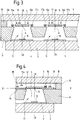
- la figure 3 est une vue en coupe selon la ligne III-III de la figure 2;
- la figure 4 est une vue en coupe selon la ligne IV-IV de la figure 2;
- la figure 5 est une vue en perspective à très grande échelle d'un microvolet et de ses électrodes de commande associées;
- la figure 6 montre très schématiquement et à petite échelle une unité de commutation de lumière incorporant un réseau conçu selon l'invention;
- la figure 7 est une vue en plan de l'unité de la figure 6;
- la figure 8 montre schématiquement comment-des unités multiples selon les figures 6 et 7 peuvent être utilisées en combinaison pour former un dispositif de distribution de lumière;
- la figure 9 montre par une vue schématique, de nouveau à très grande échelle, une variante de réalisation de l'invention; et
- la figure 10 montre une variante de réalisation d'un obturateur selon l'invention.
- FIG. 1 schematically shows two individual shutters of a network according to the invention, the microvalve of one of these shutters being in the activated position, that of the other being in its non-activated position;
- Figure 2 is a plan view, greatly enlarged, of four shutters of a network according to the invention;
- Figure 3 is a sectional view along line III-III of Figure 2;
- Figure 4 is a sectional view along line IV-IV of Figure 2;
- FIG. 5 is a perspective view on a very large scale of a microvalve and its associated control electrodes;
- Figure 6 shows very schematically and on a small scale a light switching unit incorporating a network designed according to the invention;
- Figure 7 is a plan view of the unit of Figure 6;
- Figure 8 schematically shows how multiple units according to Figures 6 and 7 can be used in combination to form a light distribution device;
- Figure 9 shows a schematic view, again on a very large scale, an alternative embodiment of the invention; and
- Figure 10 shows an alternative embodiment of a shutter according to the invention.
On va tout d'abord se référer à la figure 1 qui montre le principe de construction et de fonctionnement d'un réseau 1 d'obturateurs de lumière selon l'invention, conformément à une première variante de réalisation.We will first refer to Figure 1 which shows the principle of construction and operation of a
Les obturateurs 1a, 1b ...définissent chacun un trajet optique X-X qui est de préférence parallèle à la direction générale de la lumière incidente L frappant le réseau. Il est clair que ce dernier comprend un grand nombre d'obturateurs 1a, 1b ....etc. coopérant ensemble et disposés, par exemple, selon une matrice.The shutters 1a, 1b ... each define an optical path X-X which is preferably parallel to the general direction of the incident light L striking the grating. It is clear that the latter includes a large number of shutters 1a, 1b .... etc. cooperating together and arranged, for example, in a matrix.
Le réseau 1 comprend une plaque transparente 2, de préférence en verre, par laquelle entre le faisceau de lumière L. Du côté opposé, le réseau comprend une plaque de sortie 3, également transparente et de préférence en verre, à travers laquelle sort de la lumière Lm modulée en fonction du mode de commande du réseau (par exemple matriciel).The
Chaque obturateur 1a, 1b,.... comporte, centrés sur le trajet optique X-X qui lui est associé, une lentille de focalisation convergente 4, un micro-volet 5 percé d'un diaphragme 6 et présentant une surface réfléchissante 7, ainsi qu'une surface réfléchissante supplémentaire 8 qui est réalisée sur la lentille 4.Each shutter 1a, 1b, .... comprises, centered on the optical path XX which is associated with it, a converging focusing
Sur la figure 1, l'obturateur 1a est dans une configuration dite non activée, ce qui veut dire qu'aucune tension de commande ne lui est appliquée. Cela veut dire aussi, dans le contexte du mode de réalisation décrit ici, que l'obturateur laisse passer de la lumière à travers son diaphragme 6, la lumière incidente L étant d'abord focalisée par la lentille 4, renvoyée vers l'arrière par la surface réfléchissante 7 du microvolet 5, renvoyée de nouveau vers l'avant par la surface réfléchissante supplémentaire 8, et enfin envoyée vers l'extérieur à travers le diaphragme 6 pour passer à travers la plaque de support 3 et devenir une composante du faisceau de lumière modulée Lm.In FIG. 1, the shutter 1a is in a so-called non-activated configuration, which means that no control voltage is not applied to it. This also means, in the context of the embodiment described here, that the shutter allows light to pass through its
Par contre, l'obturateur 1b est représenté dans sa configuration dite activée dans laquelle son microvolet 5 est tourné d'un angle faible (7° par exemple) autour d'un axe Y-Y (non indiqué sur la figure 1) qui est perpendiculaire à l'axe X-X. Pour atteindre cette configuration, une tension de commande doit être appliquée à l'obturateur; ce qui va être décrit en détail plus loin.On the other hand, the shutter 1b is represented in its so-called activated configuration in which its
On voit que la configuration activée conduit à dévier le faisceau de lumière renvoyé par la surface réfléchissante 7 présente sur le microvolet 5 et préalablement focalisé par la lentille 4, en dehors du champ propre à la surface réfléchissante supplémentaire 8. Celle-ci n'est donc plus en mesure de faire passer la lumière à travers le diaphragme 6.We see that the activated configuration leads to deflecting the light beam returned by the reflecting
La suppression de la tension de commande replace le microvolet 5 dans sa position initiale (celle de l'obturateur 1a), grâce à la force élastique de déformation engendrée dans les attaches du microvolet; ce qui sera décrit en détail par la suite.The removal of the control voltage returns the
Il est donc clair que la disposition nouvelle préconisée par l'invention conduit à une commande franche par tout ou rien des points matérialisés par les diaphragmes 6 des obturateurs, la configuration non activée correspondant du côté de la plaque de sortie 3 à la présence d'un point lumineux et le cas inverse à l'absence d'un tel point.It is therefore clear that the new arrangement recommended by the invention leads to a frank control by all or nothing of the points materialized by the
Les termes "non activé" et "activé" utilisés dans la présente description ne doivent pas être pris au sens strict. En effet, ils désignent simplement la présence, respectivement l'absence, de lumière à la sortie d'un obturateur, situations qui peuvent être obtenues, soit par la présence soit par l'absence d'une tension de commande selon la configuration et la forme des électrodes qui sont associées à chaque microvolet.The terms "not activated" and "activated" used in the present description should not be taken in the strict sense. Indeed, they simply designate the presence, respectively the absence, of light at the outlet of a shutter, situations which can be obtained, either by the presence or by the absence of a control voltage according to the configuration and the forms electrodes which are associated with each microvolet.
On va se référer maintenant aux figures 2 à 5 qui illustrent plus précisément une construction préférée du réseau selon l'invention.We will now refer to Figures 2 to 5 which illustrate more precisely a preferred construction of the network according to the invention.
Comme déjà indiqué à propos de la figure 1, le réseau comprend une plaque d'entrée 2 et une plaque de sortie 3. Entre ces plaques 2 et 3 est disposée une plaquette 9 formant substrat qui est de préférence en silicium. Cette plaquette 9 est micro-usinée pour y former les microvolets 5 et les ensembles d'électrodes qui leur sont associés.As already indicated with reference to FIG. 1, the network comprises an
Un cadre 10 formant entretoise ceinture le réseau de microvolets et maintient une distance définie entre la plaque de sortie 3 et la plaquette 9.A
Un procédé préféré de micro-usinage pouvant être utilisé pour obtenir les formes souhaitées dans cette plaquette 9, est décrit dans les brevets et articles précités et il n'est donc pas nécessaire d'y revenir dans la présente description.A preferred micromachining process which can be used to obtain the desired shapes in this
Comme on peut le constater sur la figure 2, le réseau 1 est matriciel avec des rangées Ra, Rb, Rc... et des colonnes Ca, Cb, Cc...d'obturateurs resp. Ra-1, Ra-2, Ra-3....,Rb-1, Rb-2, Rb-3... etc., les rangées pouvant comporter typiquement 100 obturateurs et le nombre de rangées pouvant être de 50, par exemple dans un même réseau.As can be seen in Figure 2, the
La figure 5 qui est une vue en perspective d'un seul microvolet 5 et de ses électrodes, montre clairement que le microvolet 5 est disposé dans une ouverture 11 pratiquée dans la plaquette 9 et qu'il est attaché à celle-ci par deux attaches (ou bras de suspension) élastiques 12 alignées selon l'axe Y-Y perpendiculaire à l'axe optique X-X de l'obturateur considéré, cet axe Y-Y étant l'axe de rotation du microvolet 3.FIG. 5 which is a perspective view of a
Parallèlement à l'axe Y-Y s'étendent (voir figures 2 et 5):
- une électrode de
commande 13 reliée à un conducteur commun de commande 14 (figure 2) courant le long de la rangée de microvolets considérée; - deux électrodes de
butée 15a et 15b connectées en commun par unconducteur 15c à unconducteur 16 qui relie électriquement, par l'intermédiaire de leurs attaches conductrices 12, tous lesmicrovolets 5 d'une même colonne du réseau; - deux électrodes de
maintien 17a et 17b qui s'étendent dans la direction des colonnes le long des bords opposés de l'ouverture 11. Ces électrodes sont reliées ensemble par rangée grâce àun conducteur commun 18.
- a
control electrode 13 connected to a common control conductor 14 (FIG. 2) running along the row of microvolets considered; - two
stop electrodes conductor 15c to aconductor 16 which electrically connects, by means of theirconductive clips 12, all themicrovolets 5 of the same column of the network; - two holding
electrodes opening 11. These electrodes are connected together in rows by means of acommon conductor 18.
Les électrodes de commande 13 et de butée 15a et 15b s'étendent en travers de l'ouverture 11 au dessus de chaque microvolet 5. Par ailleurs, les conducteurs 16 croisent les conducteurs 14 et 18 sans être connectés électriquement à ceux-ci.The
Comme cela apparaît clairement à la figure 6 du premier des articles précités de V.P. Jaecklin et al., la caractéristique du déplacement en fonction de la tension de commande d'un microvolet, tel qu'utilisé dans la présente invention, présente une hystérèse. De ce fait, il est alors possible de réaliser un adressage matriciel, tel, par exemple, que celui décrit dans le brevet européen précité, au moyen d'une combinaison judicieuse d'électrodes et de tensions de commande appropriées.As clearly appears in FIG. 6 of the first of the aforementioned articles by VP Jaecklin et al., The characteristic of the displacement as a function of the control voltage of a microvolet, as used in the present invention, exhibits a hysteresis. Therefore, it is then possible to carry out a matrix addressing, such, for example, as that described in the aforementioned European patent, by means of a judicious combination of electrodes and appropriate control voltages.
On constate donc que le réseau conçu de cette manière peut être commandée de façon matricielle en appliquant aux conducteurs 14, 16 et 18 des signaux appropriées sous forme binaire. Ainsi, le réseau permet de transformer un faisceau lumineux large en une série de points lumineux en matrice dont chaque point peut être commandé individuellement.It can therefore be seen that the network designed in this way can be controlled in a matrix fashion by applying to the
Les surfaces réfléchissantes 7 et 8 sont avantageusement réalisées sous la forme de couches d'aluminium déposées par des techniques d'évaporation ou de pulvérisation. Les lentilles 4 peuvent être formées directement par micro-usinage dans la plaque d'entrée 2, par exemple sous la forme de lentilles de Fresnel, au centre desquelles sont respectivement prévues les couches formant les surfaces réfléchissantes supplémentaires 8. Les lentilles peuvent également être rèalisées sous la forme d'éléments optiques diffractants.The
A titre d'exemple, un microvolet du réseau 1 peut avoir une forme carrée de 100 microns de côté, le diaphragme 6 étant circulaire et ayant un diamètre choisi entre 5 et 20 microns. Vu le faible angle de rotation des microvolets, le temps de commutation de chaque obturateur peut être de 50 microsecondes seulement avec une tension de commande de 15 Volts.By way of example, a microvolet of the
Un exemple d'application d'un réseau 1 selon l'invention est représenté sur les figures 6 et 7. Dans ce cas, il est placé dans une capsule 19 opaque en forme de boîte cylindrique dont le fond 20 est percé, de manière qu'un faisceau de lumière puisse y être introduit à partir d'une fibre optique 21. Le réseau 1 est placé dans l'ouverture de la capsule 19, une lentille collimatrice 22 étant placée dans son voisinage pour former, à partir du faisceau entrant, un faisceau collimaté irradiant le réseau 1. A titre d'exemple, celui-ci peut comprendre 100 obturateurs par rangée et 50 obturateurs par colonne. La figure 7 montre schématiquement et en plan comment le réseau 1 et la lentille 22 peuvent être associés, le fond 20 de la capsule étant supposé enlevé.An example of application of a
La figure 8 montre une application d'une série de capsules 19 selon les figures 6 et 7 pour constituer un dispositif de distribution de lumière. Dans ce cas une source lumineuse 23 est connectée par un faisceau 24 de fibres optiques à une rangée de capsules 19. Cette disposition permet par exemple l'impression de pages à haute définition en faisant défiler un support photosensible devant la rangée de capsules, chaque réseau de microvolets étant convenablement commandé comme décrit ci-dessus.Figure 8 shows an application of a series of
On peut également envisager d'utiliser un réseau 1 de grandes dimensions pour la projection d'images du type télévision. Dans ce cas, un réseau modulateur de lumière selon l'invention pourrait assurer la haute définition en prévoyant pour chaque composante couleur un réseau comprenant un très grand nombre d'obturateurs.One can also consider using a
La figure 9 représente une variante de l'invention réalisable au niveau de chaque obturateur dans le réseau. Dans ce cas, un microvolet 5A, avec sa surface réfléchissante 7A, est placé au centre de la lentille focalisatrice 4A, tandis que le miroir supplémentaire 8A est prévu du côté opposé et pourvu du diaphragme 6A.FIG. 9 shows a variant of the invention which can be produced at each shutter in the network. In this case, a
La figure 10 représente un autre mode de réalisation de l'invention qui, du point de vue optique, est semblable au mode de réalisation des figures 3 à 5, mais qui en diffère par sa construction. Dans ce cas, le réseau d'obturateurs est réalisé directement sur la plaque de sortie 3 au lieu de l'être dans une plaquette de silicium distincte. Le réseau est alors construit à l'aide de minces couches de polysilicium présentant les mêmes électrodes que sur les figures 3 à 5. Il peut être souhaitable non seulement dans ce mode de réalisation, mais également dans ceux décrits ci-dessus, de prévoir en supplément une électrode dite de compensation indiquée par la référence 25 sur la figure 10. Cette électrode a pour but de maintenir le microvolet 5 dans sa position horizontale, lorsqu'il est à l'état de repos. En effet, il peut se produire qu'en l'absence de toute tension de commande, ce dernier soit légèrement tourné.FIG. 10 represents another embodiment of the invention which, from an optical point of view, is similar to the embodiment of FIGS. 3 to 5, but which differs therefrom in its construction. In this case, the network of shutters is produced directly on the
Bien entendu, d'autres variantes de réalisation sont possibles dans le cadre de la présente invention.Of course, other alternative embodiments are possible within the scope of the present invention.
Claims (10)
Applications Claiming Priority (2)
| Application Number | Priority Date | Filing Date | Title |
|---|---|---|---|
| FR9310960 | 1993-09-13 | ||
| FR9310960A FR2710161B1 (en) | 1993-09-13 | 1993-09-13 | Miniature array of light shutters. |
Publications (2)
| Publication Number | Publication Date |
|---|---|
| EP0643378A1 true EP0643378A1 (en) | 1995-03-15 |
| EP0643378B1 EP0643378B1 (en) | 1997-12-17 |
Family
ID=9450871
Family Applications (1)
| Application Number | Title | Priority Date | Filing Date |
|---|---|---|---|
| EP94114127A Expired - Lifetime EP0643378B1 (en) | 1993-09-13 | 1994-09-08 | Light-microshutter array |
Country Status (9)
| Country | Link |
|---|---|
| US (1) | US5579149A (en) |
| EP (1) | EP0643378B1 (en) |
| JP (1) | JP3485206B2 (en) |
| DE (1) | DE69407370T2 (en) |
| DK (1) | DK0643378T3 (en) |
| ES (1) | ES2113019T3 (en) |
| FI (1) | FI114509B (en) |
| FR (1) | FR2710161B1 (en) |
| NO (1) | NO309215B1 (en) |
Families Citing this family (148)
| Publication number | Priority date | Publication date | Assignee | Title |
|---|---|---|---|---|
| US5835255A (en) * | 1986-04-23 | 1998-11-10 | Etalon, Inc. | Visible spectrum modulator arrays |
| US6674562B1 (en) | 1994-05-05 | 2004-01-06 | Iridigm Display Corporation | Interferometric modulation of radiation |
| US6040937A (en) * | 1994-05-05 | 2000-03-21 | Etalon, Inc. | Interferometric modulation |
| US20010003487A1 (en) * | 1996-11-05 | 2001-06-14 | Mark W. Miles | Visible spectrum modulator arrays |
| US8014059B2 (en) | 1994-05-05 | 2011-09-06 | Qualcomm Mems Technologies, Inc. | System and method for charge control in a MEMS device |
| US7123216B1 (en) | 1994-05-05 | 2006-10-17 | Idc, Llc | Photonic MEMS and structures |
| US6710908B2 (en) | 1994-05-05 | 2004-03-23 | Iridigm Display Corporation | Controlling micro-electro-mechanical cavities |
| US6680792B2 (en) | 1994-05-05 | 2004-01-20 | Iridigm Display Corporation | Interferometric modulation of radiation |
| US6046840A (en) | 1995-06-19 | 2000-04-04 | Reflectivity, Inc. | Double substrate reflective spatial light modulator with self-limiting micro-mechanical elements |
| US7907319B2 (en) | 1995-11-06 | 2011-03-15 | Qualcomm Mems Technologies, Inc. | Method and device for modulating light with optical compensation |
| US5916179A (en) * | 1997-04-18 | 1999-06-29 | Sharrock; Nigel | System and method for reducing iatrogenic damage to nerves |
| GB2328312B (en) * | 1997-08-14 | 1999-08-04 | John Quentin Phillipps | Mirror controlled display device |
| US6191882B1 (en) | 1997-09-22 | 2001-02-20 | Creo Srl | Micromachined linear light valve |
| WO1999052006A2 (en) | 1998-04-08 | 1999-10-14 | Etalon, Inc. | Interferometric modulation of radiation |
| US8928967B2 (en) | 1998-04-08 | 2015-01-06 | Qualcomm Mems Technologies, Inc. | Method and device for modulating light |
| DE69834847T2 (en) * | 1998-09-24 | 2007-02-15 | Reflectivity Inc., Santa Clara | REFLECTIVE SPATIAL LIGHT MODULATOR WITH DOUBLE SUBSTRATE AND SELF-RESTRICTING MICROMECHANICAL ELEMENTS |
| CN100343717C (en) * | 1998-09-24 | 2007-10-17 | 反射公司 | Double-layer dielectric reflective space optical modulator with self-limiting micro-mechanical component |
| US6529310B1 (en) | 1998-09-24 | 2003-03-04 | Reflectivity, Inc. | Deflectable spatial light modulator having superimposed hinge and deflectable element |
| US6201633B1 (en) | 1999-06-07 | 2001-03-13 | Xerox Corporation | Micro-electromechanical based bistable color display sheets |
| JP3643508B2 (en) * | 1999-09-28 | 2005-04-27 | 株式会社東芝 | Movable film type display device |
| WO2003007049A1 (en) * | 1999-10-05 | 2003-01-23 | Iridigm Display Corporation | Photonic mems and structures |
| US6396619B1 (en) | 2000-01-28 | 2002-05-28 | Reflectivity, Inc. | Deflectable spatial light modulator having stopping mechanisms |
| US6741383B2 (en) | 2000-08-11 | 2004-05-25 | Reflectivity, Inc. | Deflectable micromirrors with stopping mechanisms |
| US6535318B1 (en) | 1999-11-12 | 2003-03-18 | Jds Uniphase Corporation | Integrated optoelectronic devices having pop-up mirrors therein and methods of forming and operating same |
| WO2001048549A1 (en) * | 1999-12-23 | 2001-07-05 | Alcatel | Shutter for satellite tracking antenna |
| US6443637B1 (en) | 2000-03-15 | 2002-09-03 | Eastman Kodak Company | Camera with electrostatic light valve that functions as diaphragm |
| US6325554B1 (en) | 2000-03-15 | 2001-12-04 | Eastman Kodak Company | Camera with electrostatic light valve that functions as image reflecting mirror for viewfinder |
| JP2002006241A (en) * | 2000-06-19 | 2002-01-09 | Sony Corp | Optical switching element, switching device and image display device using the same |
| US7099065B2 (en) * | 2000-08-03 | 2006-08-29 | Reflectivity, Inc. | Micromirrors with OFF-angle electrodes and stops |
| WO2003039612A1 (en) * | 2001-11-08 | 2003-05-15 | Atrium Medical Corporation | Intraluminal device with a coating containing a therapeutic agent |
| US6574033B1 (en) | 2002-02-27 | 2003-06-03 | Iridigm Display Corporation | Microelectromechanical systems device and method for fabricating same |
| US7781850B2 (en) | 2002-09-20 | 2010-08-24 | Qualcomm Mems Technologies, Inc. | Controlling electromechanical behavior of structures within a microelectromechanical systems device |
| US7405860B2 (en) * | 2002-11-26 | 2008-07-29 | Texas Instruments Incorporated | Spatial light modulators with light blocking/absorbing areas |
| TWI289708B (en) | 2002-12-25 | 2007-11-11 | Qualcomm Mems Technologies Inc | Optical interference type color display |
| JP2010172190A (en) * | 2002-12-27 | 2010-08-05 | Nippon Signal Co Ltd:The | Planar electromagnetic actuator |
| TW570896B (en) | 2003-05-26 | 2004-01-11 | Prime View Int Co Ltd | A method for fabricating an interference display cell |
| JP3934578B2 (en) * | 2003-06-09 | 2007-06-20 | ペンタックス株式会社 | Scanning mirror, beam scanning probe |
| JP2005121906A (en) * | 2003-10-16 | 2005-05-12 | Fuji Photo Film Co Ltd | Reflection type optical modulation array element and exposure device |
| US7342705B2 (en) | 2004-02-03 | 2008-03-11 | Idc, Llc | Spatial light modulator with integrated optical compensation structure |
| US7119945B2 (en) * | 2004-03-03 | 2006-10-10 | Idc, Llc | Altering temporal response of microelectromechanical elements |
| US7706050B2 (en) | 2004-03-05 | 2010-04-27 | Qualcomm Mems Technologies, Inc. | Integrated modulator illumination |
| US7164520B2 (en) | 2004-05-12 | 2007-01-16 | Idc, Llc | Packaging for an interferometric modulator |
| US7787170B2 (en) | 2004-06-15 | 2010-08-31 | Texas Instruments Incorporated | Micromirror array assembly with in-array pillars |
| US7113322B2 (en) * | 2004-06-23 | 2006-09-26 | Reflectivity, Inc | Micromirror having offset addressing electrode |
| US7808703B2 (en) | 2004-09-27 | 2010-10-05 | Qualcomm Mems Technologies, Inc. | System and method for implementation of interferometric modulator displays |
| US7710629B2 (en) | 2004-09-27 | 2010-05-04 | Qualcomm Mems Technologies, Inc. | System and method for display device with reinforcing substance |
| US7692839B2 (en) | 2004-09-27 | 2010-04-06 | Qualcomm Mems Technologies, Inc. | System and method of providing MEMS device with anti-stiction coating |
| US20060076634A1 (en) | 2004-09-27 | 2006-04-13 | Lauren Palmateer | Method and system for packaging MEMS devices with incorporated getter |
| US7944599B2 (en) | 2004-09-27 | 2011-05-17 | Qualcomm Mems Technologies, Inc. | Electromechanical device with optical function separated from mechanical and electrical function |
| US7936497B2 (en) | 2004-09-27 | 2011-05-03 | Qualcomm Mems Technologies, Inc. | MEMS device having deformable membrane characterized by mechanical persistence |
| US7750886B2 (en) | 2004-09-27 | 2010-07-06 | Qualcomm Mems Technologies, Inc. | Methods and devices for lighting displays |
| US7372613B2 (en) | 2004-09-27 | 2008-05-13 | Idc, Llc | Method and device for multistate interferometric light modulation |
| US7355780B2 (en) * | 2004-09-27 | 2008-04-08 | Idc, Llc | System and method of illuminating interferometric modulators using backlighting |
| US7893919B2 (en) | 2004-09-27 | 2011-02-22 | Qualcomm Mems Technologies, Inc. | Display region architectures |
| US7920135B2 (en) | 2004-09-27 | 2011-04-05 | Qualcomm Mems Technologies, Inc. | Method and system for driving a bi-stable display |
| US7813026B2 (en) | 2004-09-27 | 2010-10-12 | Qualcomm Mems Technologies, Inc. | System and method of reducing color shift in a display |
| US7668415B2 (en) | 2004-09-27 | 2010-02-23 | Qualcomm Mems Technologies, Inc. | Method and device for providing electronic circuitry on a backplate |
| US7349141B2 (en) | 2004-09-27 | 2008-03-25 | Idc, Llc | Method and post structures for interferometric modulation |
| US7701631B2 (en) | 2004-09-27 | 2010-04-20 | Qualcomm Mems Technologies, Inc. | Device having patterned spacers for backplates and method of making the same |
| US8124434B2 (en) | 2004-09-27 | 2012-02-28 | Qualcomm Mems Technologies, Inc. | Method and system for packaging a display |
| US7420725B2 (en) | 2004-09-27 | 2008-09-02 | Idc, Llc | Device having a conductive light absorbing mask and method for fabricating same |
| US7289259B2 (en) | 2004-09-27 | 2007-10-30 | Idc, Llc | Conductive bus structure for interferometric modulator array |
| US7424198B2 (en) | 2004-09-27 | 2008-09-09 | Idc, Llc | Method and device for packaging a substrate |
| US8008736B2 (en) | 2004-09-27 | 2011-08-30 | Qualcomm Mems Technologies, Inc. | Analog interferometric modulator device |
| US7684104B2 (en) | 2004-09-27 | 2010-03-23 | Idc, Llc | MEMS using filler material and method |
| US7583429B2 (en) | 2004-09-27 | 2009-09-01 | Idc, Llc | Ornamental display device |
| US7916103B2 (en) | 2004-09-27 | 2011-03-29 | Qualcomm Mems Technologies, Inc. | System and method for display device with end-of-life phenomena |
| US7719500B2 (en) | 2004-09-27 | 2010-05-18 | Qualcomm Mems Technologies, Inc. | Reflective display pixels arranged in non-rectangular arrays |
| US7653371B2 (en) | 2004-09-27 | 2010-01-26 | Qualcomm Mems Technologies, Inc. | Selectable capacitance circuit |
| US7561323B2 (en) | 2004-09-27 | 2009-07-14 | Idc, Llc | Optical films for directing light towards active areas of displays |
| US8312836B2 (en) | 2004-09-28 | 2012-11-20 | Atrium Medical Corporation | Method and apparatus for application of a fresh coating on a medical device |
| US9801982B2 (en) | 2004-09-28 | 2017-10-31 | Atrium Medical Corporation | Implantable barrier device |
| US8367099B2 (en) | 2004-09-28 | 2013-02-05 | Atrium Medical Corporation | Perforated fatty acid films |
| WO2006036967A1 (en) | 2004-09-28 | 2006-04-06 | Atrium Medical Corporation | Solubilizing a drug for use in a coating |
| US9000040B2 (en) | 2004-09-28 | 2015-04-07 | Atrium Medical Corporation | Cross-linked fatty acid-based biomaterials |
| WO2006036970A2 (en) * | 2004-09-28 | 2006-04-06 | Atrium Medical Corporation | Method of thickening a coating using a drug |
| US9012506B2 (en) | 2004-09-28 | 2015-04-21 | Atrium Medical Corporation | Cross-linked fatty acid-based biomaterials |
| US8962023B2 (en) | 2004-09-28 | 2015-02-24 | Atrium Medical Corporation | UV cured gel and method of making |
| US7092143B2 (en) * | 2004-10-19 | 2006-08-15 | Reflectivity, Inc | Micromirror array device and a method for making the same |
| US7295363B2 (en) | 2005-04-08 | 2007-11-13 | Texas Instruments Incorporated | Optical coating on light transmissive substrates of micromirror devices |
| GB0510470D0 (en) * | 2005-05-23 | 2005-06-29 | Qinetiq Ltd | Coded aperture imaging system |
| US9427423B2 (en) | 2009-03-10 | 2016-08-30 | Atrium Medical Corporation | Fatty-acid based particles |
| US9278161B2 (en) | 2005-09-28 | 2016-03-08 | Atrium Medical Corporation | Tissue-separating fatty acid adhesion barrier |
| CA2626030A1 (en) | 2005-10-15 | 2007-04-26 | Atrium Medical Corporation | Hydrophobic cross-linked gels for bioabsorbable drug carrier coatings |
| US7795061B2 (en) | 2005-12-29 | 2010-09-14 | Qualcomm Mems Technologies, Inc. | Method of creating MEMS device cavities by a non-etching process |
| US7916980B2 (en) | 2006-01-13 | 2011-03-29 | Qualcomm Mems Technologies, Inc. | Interconnect structure for MEMS device |
| GB2434934A (en) * | 2006-02-06 | 2007-08-08 | Qinetiq Ltd | Processing coded aperture image data by applying weightings to aperture functions and data frames |
| GB2434937A (en) | 2006-02-06 | 2007-08-08 | Qinetiq Ltd | Coded aperture imaging apparatus performing image enhancement |
| GB2434935A (en) * | 2006-02-06 | 2007-08-08 | Qinetiq Ltd | Coded aperture imager using reference object to form decoding pattern |
| GB0602380D0 (en) * | 2006-02-06 | 2006-03-15 | Qinetiq Ltd | Imaging system |
| GB2434936A (en) | 2006-02-06 | 2007-08-08 | Qinetiq Ltd | Imaging system having plural distinct coded aperture arrays at different mask locations |
| GB2434877A (en) * | 2006-02-06 | 2007-08-08 | Qinetiq Ltd | MOEMS optical modulator |
| US7603001B2 (en) | 2006-02-17 | 2009-10-13 | Qualcomm Mems Technologies, Inc. | Method and apparatus for providing back-lighting in an interferometric modulator display device |
| US7903047B2 (en) | 2006-04-17 | 2011-03-08 | Qualcomm Mems Technologies, Inc. | Mode indicator for interferometric modulator displays |
| US7711239B2 (en) | 2006-04-19 | 2010-05-04 | Qualcomm Mems Technologies, Inc. | Microelectromechanical device and method utilizing nanoparticles |
| US7649671B2 (en) | 2006-06-01 | 2010-01-19 | Qualcomm Mems Technologies, Inc. | Analog interferometric modulator device with electrostatic actuation and release |
| US7766498B2 (en) | 2006-06-21 | 2010-08-03 | Qualcomm Mems Technologies, Inc. | Linear solid state illuminator |
| US7835061B2 (en) | 2006-06-28 | 2010-11-16 | Qualcomm Mems Technologies, Inc. | Support structures for free-standing electromechanical devices |
| US7527998B2 (en) | 2006-06-30 | 2009-05-05 | Qualcomm Mems Technologies, Inc. | Method of manufacturing MEMS devices providing air gap control |
| GB0615040D0 (en) * | 2006-07-28 | 2006-09-06 | Qinetiq Ltd | Processing method for coded apperture sensor |
| US7763546B2 (en) | 2006-08-02 | 2010-07-27 | Qualcomm Mems Technologies, Inc. | Methods for reducing surface charges during the manufacture of microelectromechanical systems devices |
| WO2008045207A2 (en) | 2006-10-06 | 2008-04-17 | Qualcomm Mems Technologies, Inc. | Light guide |
| EP2366942A1 (en) | 2006-10-06 | 2011-09-21 | Qualcomm Mems Technologies, Inc. | Optical loss layer integrated in an illumination apparatus of a display |
| US9492596B2 (en) | 2006-11-06 | 2016-11-15 | Atrium Medical Corporation | Barrier layer with underlying medical device and one or more reinforcing support structures |
| WO2008057344A2 (en) | 2006-11-06 | 2008-05-15 | Atrium Medical Corporation | Coated surgical mesh |
| US7719752B2 (en) | 2007-05-11 | 2010-05-18 | Qualcomm Mems Technologies, Inc. | MEMS structures, methods of fabricating MEMS components on separate substrates and assembly of same |
| US8068710B2 (en) | 2007-12-07 | 2011-11-29 | Qualcomm Mems Technologies, Inc. | Decoupled holographic film and diffuser |
| US7949213B2 (en) | 2007-12-07 | 2011-05-24 | Qualcomm Mems Technologies, Inc. | Light illumination of displays with front light guide and coupling elements |
| US8049951B2 (en) | 2008-04-15 | 2011-11-01 | Qualcomm Mems Technologies, Inc. | Light with bi-directional propagation |
| DE102008019600B4 (en) * | 2008-04-18 | 2021-03-04 | Fraunhofer-Gesellschaft zur Förderung der angewandten Forschung e.V. | Stacked optical device and method of making the same |
| GB0822281D0 (en) * | 2008-12-06 | 2009-01-14 | Qinetiq Ltd | Optically diverse coded aperture imaging |
| US8172417B2 (en) | 2009-03-06 | 2012-05-08 | Qualcomm Mems Technologies, Inc. | Shaped frontlight reflector for use with display |
| US20100302218A1 (en) | 2009-05-29 | 2010-12-02 | Qualcomm Mems Technologies, Inc. | Illumination devices and methods of fabrication thereof |
| US20110038910A1 (en) | 2009-08-11 | 2011-02-17 | Atrium Medical Corporation | Anti-infective antimicrobial-containing biomaterials |
| US10303035B2 (en) | 2009-12-22 | 2019-05-28 | View, Inc. | Self-contained EC IGU |
| US8213074B1 (en) | 2011-03-16 | 2012-07-03 | Soladigm, Inc. | Onboard controller for multistate windows |
| US10747082B2 (en) | 2009-12-22 | 2020-08-18 | View, Inc. | Onboard controller for multistate windows |
| US11592723B2 (en) | 2009-12-22 | 2023-02-28 | View, Inc. | Automated commissioning of controllers in a window network |
| CN102834761A (en) | 2010-04-09 | 2012-12-19 | 高通Mems科技公司 | Mechanical layer and methods of forming the same |
| WO2012009707A2 (en) | 2010-07-16 | 2012-01-19 | Atrium Medical Corporation | Composition and methods for altering the rate of hydrolysis of cured oil-based materials |
| US10989977B2 (en) | 2011-03-16 | 2021-04-27 | View, Inc. | Onboard controller for multistate windows |
| US11415949B2 (en) | 2011-03-16 | 2022-08-16 | View, Inc. | Security event detection with smart windows |
| US11703814B2 (en) | 2011-03-16 | 2023-07-18 | View, Inc. | Security event detection with smart windows |
| US8705162B2 (en) | 2012-04-17 | 2014-04-22 | View, Inc. | Controlling transitions in optically switchable devices |
| US11822202B2 (en) | 2011-03-16 | 2023-11-21 | View, Inc. | Controlling transitions in optically switchable devices |
| US11054792B2 (en) * | 2012-04-13 | 2021-07-06 | View, Inc. | Monitoring sites containing switchable optical devices and controllers |
| US8963159B2 (en) | 2011-04-04 | 2015-02-24 | Qualcomm Mems Technologies, Inc. | Pixel via and methods of forming the same |
| US9134527B2 (en) | 2011-04-04 | 2015-09-15 | Qualcomm Mems Technologies, Inc. | Pixel via and methods of forming the same |
| JP5803615B2 (en) * | 2011-11-29 | 2015-11-04 | 富士通株式会社 | Electronic device and manufacturing method thereof |
| EP3611707B1 (en) | 2012-04-13 | 2024-01-17 | View, Inc. | Applications for controlling optically switchable devices |
| US10964320B2 (en) | 2012-04-13 | 2021-03-30 | View, Inc. | Controlling optically-switchable devices |
| US11255120B2 (en) | 2012-05-25 | 2022-02-22 | View, Inc. | Tester and electrical connectors for insulated glass units |
| US9867880B2 (en) | 2012-06-13 | 2018-01-16 | Atrium Medical Corporation | Cured oil-hydrogel biomaterial compositions for controlled drug delivery |
| US11868103B2 (en) | 2014-03-05 | 2024-01-09 | View, Inc. | Site monitoring system |
| US11150616B2 (en) | 2014-03-05 | 2021-10-19 | View, Inc. | Site monitoring system |
| CA2941526C (en) * | 2014-03-05 | 2023-02-28 | View, Inc. | Monitoring sites containing switchable optical devices and controllers |
| EP3705937B1 (en) | 2014-06-30 | 2023-03-15 | View, Inc. | Computer-implemented control methods and systems for networks of optically switchable windows during reduced power availability |
| US11003041B2 (en) | 2014-06-30 | 2021-05-11 | View, Inc. | Power management for electrochromic window networks |
| US11740948B2 (en) | 2014-12-08 | 2023-08-29 | View, Inc. | Multiple interacting systems at a site |
| EP3926572A1 (en) | 2014-12-08 | 2021-12-22 | View, Inc. | Multiple interacting systems at a site |
| DE102015112296A1 (en) * | 2015-07-28 | 2017-02-02 | Valeo Schalter Und Sensoren Gmbh | Optical sensor device for a motor vehicle, motor vehicle and method |
| US11384596B2 (en) | 2015-09-18 | 2022-07-12 | View, Inc. | Trunk line window controllers |
| CA3039342A1 (en) | 2016-10-03 | 2018-04-12 | View, Inc. | Site monitoring system |
| US11300849B2 (en) | 2017-04-26 | 2022-04-12 | View, Inc. | Tintable window system computing platform used for personal computing |
| US11747696B2 (en) | 2017-04-26 | 2023-09-05 | View, Inc. | Tandem vision window and media display |
| US10571683B2 (en) * | 2017-11-28 | 2020-02-25 | Aptiv Technologies Limited | Multi-faceted MEMS mirror device useful for vehicle LIDAR |
| TW202206925A (en) | 2020-03-26 | 2022-02-16 | 美商視野公司 | Access and messaging in a multi client network |
| US11631493B2 (en) | 2020-05-27 | 2023-04-18 | View Operating Corporation | Systems and methods for managing building wellness |
Citations (6)
| Publication number | Priority date | Publication date | Assignee | Title |
|---|---|---|---|---|
| US4383255A (en) * | 1980-03-11 | 1983-05-10 | Centre Electronique Horloger S.A. | Miniature display device |
| FR2542105A1 (en) * | 1983-03-04 | 1984-09-07 | Canon Kk | OPTICAL MODULATION ELEMENT AND ITS CONTROL METHOD |
| EP0143079A2 (en) * | 1983-11-18 | 1985-05-29 | Centre Electronique Horloger S.A. | Method of producing a microvalve device and application of this method for obtaining a light modulator |
| US4566935A (en) * | 1984-07-31 | 1986-01-28 | Texas Instruments Incorporated | Spatial light modulator and method |
| EP0453400A1 (en) * | 1990-04-20 | 1991-10-23 | Centre Suisse D'electronique Et De Microtechnique S.A. | Matrix-addressed light modulation device |
| EP0469293A1 (en) * | 1990-06-29 | 1992-02-05 | Texas Instruments Incorporated | Multi-level deformable mirror device |
Family Cites Families (7)
| Publication number | Priority date | Publication date | Assignee | Title |
|---|---|---|---|---|
| US4087810A (en) * | 1976-06-30 | 1978-05-02 | International Business Machines Corporation | Membrane deformographic display, and method of making |
| US4420896A (en) * | 1981-09-17 | 1983-12-20 | General Electric Company | Method for fabrication of electroscopic display devices and transmissive display devices fabricated thereby |
| US4571603A (en) * | 1981-11-03 | 1986-02-18 | Texas Instruments Incorporated | Deformable mirror electrostatic printer |
| EP0246547A3 (en) * | 1986-05-22 | 1990-06-13 | Siemens Aktiengesellschaft | Optical image-processing arrangement |
| DE3741856C1 (en) * | 1987-12-10 | 1989-04-20 | Messerschmitt Boelkow Blohm | Optronic protected missile detection |
| US5101236A (en) * | 1989-12-21 | 1992-03-31 | Texas Instruments Incorporated | Light energy control system and method of operation |
| GB9107144D0 (en) * | 1991-04-05 | 1991-05-22 | Rank Cintel Ltd | Recording video signals on cinematographic film |
-
1993
- 1993-09-13 FR FR9310960A patent/FR2710161B1/en not_active Expired - Fee Related
-
1994
- 1994-09-08 EP EP94114127A patent/EP0643378B1/en not_active Expired - Lifetime
- 1994-09-08 DE DE69407370T patent/DE69407370T2/en not_active Expired - Lifetime
- 1994-09-08 ES ES94114127T patent/ES2113019T3/en not_active Expired - Lifetime
- 1994-09-08 DK DK94114127T patent/DK0643378T3/en active
- 1994-09-12 NO NO943381A patent/NO309215B1/en not_active IP Right Cessation
- 1994-09-12 US US08/304,689 patent/US5579149A/en not_active Expired - Lifetime
- 1994-09-12 FI FI944198A patent/FI114509B/en not_active IP Right Cessation
- 1994-09-13 JP JP24344494A patent/JP3485206B2/en not_active Expired - Lifetime
Patent Citations (6)
| Publication number | Priority date | Publication date | Assignee | Title |
|---|---|---|---|---|
| US4383255A (en) * | 1980-03-11 | 1983-05-10 | Centre Electronique Horloger S.A. | Miniature display device |
| FR2542105A1 (en) * | 1983-03-04 | 1984-09-07 | Canon Kk | OPTICAL MODULATION ELEMENT AND ITS CONTROL METHOD |
| EP0143079A2 (en) * | 1983-11-18 | 1985-05-29 | Centre Electronique Horloger S.A. | Method of producing a microvalve device and application of this method for obtaining a light modulator |
| US4566935A (en) * | 1984-07-31 | 1986-01-28 | Texas Instruments Incorporated | Spatial light modulator and method |
| EP0453400A1 (en) * | 1990-04-20 | 1991-10-23 | Centre Suisse D'electronique Et De Microtechnique S.A. | Matrix-addressed light modulation device |
| EP0469293A1 (en) * | 1990-06-29 | 1992-02-05 | Texas Instruments Incorporated | Multi-level deformable mirror device |
Non-Patent Citations (4)
| Title |
|---|
| K.E.PETERSEN: "micromecanical light deflector array", IBM TECNICAL DISCLOSURE BULLETIN, vol. 20, no. 1, June 1977 (1977-06-01), US, pages 355 - 356 * |
| L.J.HORNBECK: "deformable mirror spatial light modulators", SPATIAL LIGHT MODULATORS AND APPLICATIONS, August 1989 (1989-08-01), SAN DIEGO CA US, pages 86 - 102, XP000351394 * |
| R.VUILLEUMIER: "novel electromechanical microshutter display device", EURODISPLAY, September 1984 (1984-09-01), PARIS FRANCE, pages 441 - 44 * |
| V.P.JAECKLIN: "optical microshutter and torsional micromirrors for nlight modulator arrays", MEMS, 10 February 1993 (1993-02-10), FT. LAUDERDALE EUA, pages 124 - 127 * |
Also Published As
| Publication number | Publication date |
|---|---|
| US5579149A (en) | 1996-11-26 |
| DE69407370T2 (en) | 1998-07-09 |
| FR2710161B1 (en) | 1995-11-24 |
| FI944198A (en) | 1995-03-14 |
| NO943381L (en) | 1995-03-14 |
| FR2710161A1 (en) | 1995-03-24 |
| FI944198A0 (en) | 1994-09-12 |
| ES2113019T3 (en) | 1998-04-16 |
| NO943381D0 (en) | 1994-09-12 |
| JP3485206B2 (en) | 2004-01-13 |
| DK0643378T3 (en) | 1998-08-24 |
| JPH07181404A (en) | 1995-07-21 |
| EP0643378B1 (en) | 1997-12-17 |
| FI114509B (en) | 2004-10-29 |
| DE69407370D1 (en) | 1998-01-29 |
| NO309215B1 (en) | 2000-12-27 |
Similar Documents
| Publication | Publication Date | Title |
|---|---|---|
| EP0643378B1 (en) | Light-microshutter array | |
| EP0610185B1 (en) | Optical modulation device having variable-sized cells | |
| US7116463B2 (en) | High angular deflection micro-mirror system | |
| US6337760B1 (en) | Encapsulated multi-directional light beam steering device | |
| EP0136193A1 (en) | Optical switch making use of the displacement of a fluid and apparatus for composing a line of points | |
| EP1637914B1 (en) | Locally deformable mirror comprising electroactive material whose thickness can be varied by means of electrical effects | |
| US20040114209A1 (en) | High frequency deformable mirror device | |
| WO1998020390A1 (en) | Display device and flat television screen using this device | |
| FR2731084A1 (en) | METHOD AND DEVICE FOR CONTROLLING A MIRROR IN A MICRO-MIRROR NETWORK | |
| US7095545B2 (en) | Microelectromechanical device with reset electrode | |
| KR20010106484A (en) | A double substrate reflective spatial light modulator with self-limiting micro-mechanical elements | |
| FR2737595A1 (en) | LIQUID CRYSTAL DISPLAY DEVICE | |
| JP4404174B2 (en) | Optical switching element, switching device using the same, and image display device | |
| EP2277074A1 (en) | Informative eyeglasses | |
| EP0881527A1 (en) | Spatial optical switching system using a multichannel acousto-optic deflector | |
| JP2001183591A (en) | Micromirror optical switch | |
| WO1993025926A1 (en) | Omnidirectional surveillance device with optimal coverage of surrounding space by means of contiguous fields | |
| WO1993009463A1 (en) | Device for microscanning and infrared camera provided with such device | |
| JP4718740B2 (en) | Optical add / drop multiplexer | |
| US7652811B2 (en) | Small mechanical optical shutter with non-imaging concentrating optics | |
| JPH11160635A (en) | Optical element and manufacturing method thereof and device using it | |
| Gudeman et al. | Using the Grating Light Valve device as a multichannel variable optical attenuator (VOA) for the 1.55-um spectral region | |
| WO2021064326A1 (en) | Thermo-optically addressed spatial light modulator | |
| JP2000275441A (en) | Hologram color filter and color image display device using the same | |
| WO2021005287A1 (en) | Matrix-array optical component for focusing an incident light beam on a series of points |
Legal Events
| Date | Code | Title | Description |
|---|---|---|---|
| PUAI | Public reference made under article 153(3) epc to a published international application that has entered the european phase |
Free format text: ORIGINAL CODE: 0009012 |
|
| AK | Designated contracting states |
Kind code of ref document: A1 Designated state(s): BE CH DE DK ES FR GB IT LI NL |
|
| 17P | Request for examination filed |
Effective date: 19950817 |
|
| 17Q | First examination report despatched |
Effective date: 19960812 |
|
| GRAG | Despatch of communication of intention to grant |
Free format text: ORIGINAL CODE: EPIDOS AGRA |
|
| GRAH | Despatch of communication of intention to grant a patent |
Free format text: ORIGINAL CODE: EPIDOS IGRA |
|
| GRAH | Despatch of communication of intention to grant a patent |
Free format text: ORIGINAL CODE: EPIDOS IGRA |
|
| GRAA | (expected) grant |
Free format text: ORIGINAL CODE: 0009210 |
|
| AK | Designated contracting states |
Kind code of ref document: B1 Designated state(s): BE CH DE DK ES FR GB IT LI NL |
|
| REG | Reference to a national code |
Ref country code: CH Ref legal event code: EP |
|
| REF | Corresponds to: |
Ref document number: 69407370 Country of ref document: DE Date of ref document: 19980129 |
|
| ITF | It: translation for a ep patent filed |
Owner name: ING. C. GREGORJ S.P.A. |
|
| REG | Reference to a national code |
Ref country code: CH Ref legal event code: NV Representative=s name: ICB INGENIEURS CONSEILS EN BREVETS SA |
|
| GBT | Gb: translation of ep patent filed (gb section 77(6)(a)/1977) |
Effective date: 19980313 |
|
| REG | Reference to a national code |
Ref country code: ES Ref legal event code: FG2A Ref document number: 2113019 Country of ref document: ES Kind code of ref document: T3 |
|
| REG | Reference to a national code |
Ref country code: DK Ref legal event code: T3 |
|
| PLBE | No opposition filed within time limit |
Free format text: ORIGINAL CODE: 0009261 |
|
| STAA | Information on the status of an ep patent application or granted ep patent |
Free format text: STATUS: NO OPPOSITION FILED WITHIN TIME LIMIT |
|
| 26N | No opposition filed | ||
| REG | Reference to a national code |
Ref country code: CH Ref legal event code: PUE Owner name: CSEM, CENTRE SUISSE D'ELECTRONIQUE ET DE MICROTECH Ref country code: CH Ref legal event code: NV Representative=s name: CSEM CENTRE SUISSE D'ELECTRONIQUE ET DE MICROTECHN |
|
| REG | Reference to a national code |
Ref country code: GB Ref legal event code: IF02 |
|
| REG | Reference to a national code |
Ref country code: GB Ref legal event code: 732E |
|
| REG | Reference to a national code |
Ref country code: FR Ref legal event code: TP |
|
| REG | Reference to a national code |
Ref country code: ES Ref legal event code: PC2A |
|
| NLS | Nl: assignments of ep-patents |
Owner name: COLIBRYS S.A. |
|
| REG | Reference to a national code |
Ref country code: CH Ref legal event code: NV Representative=s name: CABINET ROLAND NITHARDT CONSEILS EN PROPRIETE INDU |
|
| REG | Reference to a national code |
Ref country code: CH Ref legal event code: PCAR Free format text: PATENTS & TECHNOLOGY SURVEYS SA;RUE DES TERREAUX 7 CASE POSTALE 2848;2001 NEUCHATEL (CH) |
|
| REG | Reference to a national code |
Ref country code: CH Ref legal event code: PFA Owner name: COLIBRYS SA Free format text: COLIBRYS SA#MALADIERE 83#2007 NEUCHATEL (CH) -TRANSFER TO- COLIBRYS SA#MALADIERE 83#2007 NEUCHATEL (CH) |
|
| PGFP | Annual fee paid to national office [announced via postgrant information from national office to epo] |
Ref country code: NL Payment date: 20130918 Year of fee payment: 20 Ref country code: ES Payment date: 20130927 Year of fee payment: 20 Ref country code: DK Payment date: 20130918 Year of fee payment: 20 Ref country code: DE Payment date: 20130919 Year of fee payment: 20 Ref country code: CH Payment date: 20130919 Year of fee payment: 20 |
|
| PGFP | Annual fee paid to national office [announced via postgrant information from national office to epo] |
Ref country code: GB Payment date: 20130919 Year of fee payment: 20 Ref country code: FR Payment date: 20130919 Year of fee payment: 20 |
|
| PGFP | Annual fee paid to national office [announced via postgrant information from national office to epo] |
Ref country code: BE Payment date: 20130919 Year of fee payment: 20 |
|
| PGFP | Annual fee paid to national office [announced via postgrant information from national office to epo] |
Ref country code: IT Payment date: 20130930 Year of fee payment: 20 |
|
| REG | Reference to a national code |
Ref country code: DE Ref legal event code: R071 Ref document number: 69407370 Country of ref document: DE |
|
| REG | Reference to a national code |
Ref country code: CH Ref legal event code: PL Ref country code: DK Ref legal event code: EUP Effective date: 20140908 |
|
| REG | Reference to a national code |
Ref country code: NL Ref legal event code: V4 Effective date: 20140908 |
|
| REG | Reference to a national code |
Ref country code: GB Ref legal event code: PE20 Expiry date: 20140907 |
|
| PG25 | Lapsed in a contracting state [announced via postgrant information from national office to epo] |
Ref country code: DE Free format text: LAPSE BECAUSE OF EXPIRATION OF PROTECTION Effective date: 20140909 |
|
| PG25 | Lapsed in a contracting state [announced via postgrant information from national office to epo] |
Ref country code: GB Free format text: LAPSE BECAUSE OF EXPIRATION OF PROTECTION Effective date: 20140907 |
|
| REG | Reference to a national code |
Ref country code: ES Ref legal event code: FD2A Effective date: 20150108 |
|
| PG25 | Lapsed in a contracting state [announced via postgrant information from national office to epo] |
Ref country code: ES Free format text: LAPSE BECAUSE OF EXPIRATION OF PROTECTION Effective date: 20140909 |