EP0647828A2 - Cofocal optical systems for thickness measurements of patterned wafers - Google Patents
Cofocal optical systems for thickness measurements of patterned wafers Download PDFInfo
- Publication number
- EP0647828A2 EP0647828A2 EP94307402A EP94307402A EP0647828A2 EP 0647828 A2 EP0647828 A2 EP 0647828A2 EP 94307402 A EP94307402 A EP 94307402A EP 94307402 A EP94307402 A EP 94307402A EP 0647828 A2 EP0647828 A2 EP 0647828A2
- Authority
- EP
- European Patent Office
- Prior art keywords
- wafer
- optical system
- image
- lens
- high resolution
- Prior art date
- Legal status (The legal status is an assumption and is not a legal conclusion. Google has not performed a legal analysis and makes no representation as to the accuracy of the status listed.)
- Granted
Links
Images

Classifications
-
- G—PHYSICS
- G03—PHOTOGRAPHY; CINEMATOGRAPHY; ANALOGOUS TECHNIQUES USING WAVES OTHER THAN OPTICAL WAVES; ELECTROGRAPHY; HOLOGRAPHY
- G03F—PHOTOMECHANICAL PRODUCTION OF TEXTURED OR PATTERNED SURFACES, e.g. FOR PRINTING, FOR PROCESSING OF SEMICONDUCTOR DEVICES; MATERIALS THEREFOR; ORIGINALS THEREFOR; APPARATUS SPECIALLY ADAPTED THEREFOR
- G03F7/00—Photomechanical, e.g. photolithographic, production of textured or patterned surfaces, e.g. printing surfaces; Materials therefor, e.g. comprising photoresists; Apparatus specially adapted therefor
- G03F7/70—Microphotolithographic exposure; Apparatus therefor
- G03F7/70483—Information management; Active and passive control; Testing; Wafer monitoring, e.g. pattern monitoring
-
- G—PHYSICS
- G01—MEASURING; TESTING
- G01B—MEASURING LENGTH, THICKNESS OR SIMILAR LINEAR DIMENSIONS; MEASURING ANGLES; MEASURING AREAS; MEASURING IRREGULARITIES OF SURFACES OR CONTOURS
- G01B11/00—Measuring arrangements characterised by the use of optical techniques
- G01B11/02—Measuring arrangements characterised by the use of optical techniques for measuring length, width or thickness
- G01B11/06—Measuring arrangements characterised by the use of optical techniques for measuring length, width or thickness for measuring thickness ; e.g. of sheet material
Definitions
- the present invention relates generally to film thickness measurement systems, and more particularly, to cofocal optical systems for making film thickness measurements on patterned wafers.
- a full wafer imaging system requires either a large refractive lens assembly, a parabola-based reflector system, or the use of a spherical vacuum chuck to form the wafer into a shallow sphere.
- the size of the optical elements approaches the size of the largest wafer that is to be measured.
- These large optics requirement leads to high cost and the optical elements require careful optical design.
- Forming the wafer into a shallow sphere provides an excellent way of avoiding high cost optical elements although the deformation of the wafer during chip fabrication may be viewed with suspicion and this practice will not work at all if the ambient environment is a vacuum, such as in an automated ultra-clean wafer process line.
- Prior whole-wafer film thickness mappers require measurement of multispectral reflectance over a full aperture of the imaging and these mappers generally fall into two categories.
- the entire wafer is imaged onto a NxN pixel CCD array (512x512, 1024x1024, or 2048x2048, for example) to provide a spatial resolution at the wafer plane of approximately 200 microns per pixel.
- a CCD array attached to a conventional narrow-field microscope is used provide high resolution in the 1 to 5 micron per pixel range.
- covering the whole wafer requires mechanical scanning of the entire wafer or optical head.
- the present invention combines both aspects of prior art systems into a single optical system by providing a means for imaging the full wafer at low resolution (200 microns per pixel) and also providing a means for imaging one or more high resolution subfields at a resolution in the 5 to 10 micron per pixel range at the wafer surface.
- a large feed lens or reflective optical system lens is used to image the entire wafer at lower resolution.
- Subaperture optical elements comprising either a small scanning lens or a sparse array of lenses, are used to image small areas of the wafer at higher resolution and the subaperture optical elements create an enlarged image in the same object plane as the actual wafer.
- Both areas are then imaged onto a CCD array of a CCD camera by a single lens or reflector to provide a common or cofocal feature of the present invention.
- This arrangement avoids frequent refocussing to make thickness measurements on different parts of the wafer.
- the present optical system comprises a spectrally filtered light sources for providing light to illuminate the patterned wafer.
- a low resolution imaging system is provided for imaging the wafer at a relatively low predetermined resolution.
- a high resolution imaging system is provided for imaging a subarea of the wafer at a relatively high predetermined resolution to create an enlarged image in the same object plane as the wafer.
- An image producing system is provided for producing a visual image of the wafer derived from the images provided by the low and the high resolution imaging systems.
- the present invention provides a simplified and inexpensive full-wafer imaging system that incorporates a scanning cofocal optical system to view a patterned silicon wafer at two or more different magnifications.
- This type of optical system images the whole wafer onto the CCD camera and in addition allows small magnified areas of the wafer to be viewed by the same CCD camera, wherein the full wafer and local, high resolution images are in focus at the same plane (cofocal).
- the high resolution image regions may be selected by moving the cofocal optical system (the small scanning lens or the sparse array of lenses) across the wafer .
- the present invention allows the determination of thin film thicknesses of patterned wafers, planar wafers, and silicon-on-insulator (SOI) wafers, even though the spatial frequencies of the patterns are radically different in all these cases. As stated above, it is often desirable to measure the thickness of thin film layers in features in the 10 to 100 micron lateral size range.
- the present invention retains the full wafer imaging and thickness mapping capabilities provided by conventional imaging systems and adds the ability to make thickness maps of magnified regions within a semiconductor chip as well as test pads located in scribe alleys thereon.
- the use of high resolution multispectral subimages provided by the present invention significantly increases the speed at which thickness maps of these patterned regions are generated.
- the present invention thus provides a means for making thickness determinations of films including low frequency planar layers on silicon wafers for uniformity determination, SOI wafers and particularly ones containing high slope regions, and patterned wafers where the lateral feature size is in the 10 to 100 micron range.
- the optical system of the present invention may be implemented in the form of a scanning system for performing diagnostic tests n any part of a wafer that is processed, or it may be used in a production mode wherein the subaperture optical elements (scanning lens or sparse array of lenses) makes measurements of small features at predetermined locations on the wafer, either in the chip region, the scribe alleys, or on test pads located on the surface of the wafer.
- the present invention also provides an image of the wafer which may be used for wafer alignment (i.e., determining wafer position and orientation).
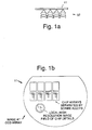
- Fig. 1 illustrates one embodiment of an optical system 10 in accordance with the principles of the present invention employing a scanning lens as a cofocal optical element thereof, and that is adapted to make film thickness measurements of a patterned wafer 11.
- the optical system 10 is comprised of a high intensity light source 12, such as a halogen lamp 12, whose output is coupled by way of a fiber optic bundle 13, for example, to a lens group comprising a concave lens 15 and a convex lens 17.
- a motor drive 21 is coupled to a filter wheel 23 and is provided to filter the light provided by the halogen lamp 12.
- the filter wheel 23 is adapted to insert one of a plurality of filters 16 between the concave lens 15 and a convex lens 17.
- the filters 16 are employed to filter the light from the light source 12 and provide for illuminating light in selected regions of the spectrum.
- the use of the high intensity light source 12 and the filter wheel 23 provides for a spectrally filtered light source 18.
- the output of the a convex lens 17 is applied to a collimating lens 31 that may be made of plastic, for example, that collimates the filtered light from the halogen lamp 12 and images it through a ground glass plate or surface 32 that acts as a diffuser 32.
- the diffuser 32 causes the light to scatter and produces a forward scatter envelope 36 for each point of light projected by the collimating lens 31.
- the light output from the diffuser 32 is applied to a beamsplitter 33 and the the reflected portion of the light illuminates a wafer 11.
- the light incident on the wafer 11 is reflected therefrom and this light is imaged by a zoom lens 34 through the beamsplitter 33 on onto a CCD array 35 of a CCD camera 35a.
- a moveable cofocal optical system 37 comprising one of a plurality of subaperture optical elements, and which may be comprise a small scanning lens system 37 or a sparse array of lenses 37 (shown in Fig. 1a) is used to image small areas of the wafer 11 at higher resolution.
- the subaperture optical elements create an enlarged image in the same object plane as the wafer 11 and that is viewed by the camera 35a.
- the zoom lens 34 provides a means for imaging the full wafer at 200 microns per pixel resolution, for example, and the moveable cofocal optical system 37 provides a means for imaging the surface of the wafer 11 to provide for one or more high resolution subfields at a resolution in the 5 to 10 micron per pixel range, for example, at the surface of the wafer 11.
- Fig. 1a shows a portion of the optical system 10 that includes a cofocal optical system 37 that comprises the sparse array of lenses 37 in place of the small scanning lens system 37.
- the design of the sparse array of lenses 37 is considered routine to those skilled in the art and will not be described in detail herein.
- the optical system 10 of Figs. 1 and 1a are designed to provide two distinct functions.
- First the optical system 10 allows wafers having up to a 200 mm diameter to be illuminated by diffuse light from the spectrally filtered light source 18.
- the diffused nature of the incident light at the wafer 11 eliminates the need to mount the wafer 11 on a vacuum chuck, since light is incident on the wafer 11 at a large range of angles.
- the small moveable cofocal optical systems 37 may be placed anywhere in front of the wafer 11 under test to allow higher spatial resolution measurements of film thickness to be made over selected regions when diagnostic wafer measurements are made. Process control measurements usually require measurements at fixed locations and this may be accomplished by using multiple optical cofocal assemblies in the form of the sparse array of lenses 37 placed over the regions of interest.
- the present invention eliminates the requirement for large high quality optical elements and additionally does not require that the wafer 11 be vacuum-chucked to a flat or spherical shape, to match the field curvature of the investigating optical system.
- the spectrally variable light source 18 used in the optical system 10 may be comprised of a 150 watt halogen. lamp 12, for example, whose light output is coupled through the optical filter 16 by a conventional fiber optic light waveguide comprising the fiber optic bundle 13. This arrangement is adapted to sequentially illuminate the surface of the wafer 11 with a large number of narrow band wavelengths of light.
- the light from the filtered light source 18 is expanded and roughly collimated by the relatively large plastic collimating lens 31 and scattered by the ground glass screen 32 or diffuser 32 onto the surface of the wafer 11.
- the plastic collimating lens 31 improves the illumination uniformity, and it has a size that is at least equal to the size the largest wafer 11 that is to be measured.
- the relatively large beamsplitter 33 may be made of window glass coated with a partially transparent protected silver coating, and is used to collect light reflected from the wafer 11 and direct it to the zoom lens 34 and CCD camera 35a which views the entire wafer 11.
- the present system 10 has been assembled in a laboratory environment and provides high light levels at the CCD camera 35a as well as excellent digitized images of SOI and planar coated wafers 11.
- the CCD camera 35a used in a reduced to practice embodiment of the optical system 10 comprises a 512 x 512 CCD array 35 which can only resolve 400 microns at the wafer 11 if the entire 200 mm wafer 11 is matched to the maximum array size (1024x1024). Images of patterned wafers 11 have small rectangular features in the micron level cannot be resolved at this low magnification. These features are resolved by employing the small cofocal optical system 37 disposed near the surface of the wafer 11. The cofocal optical system 37 is designed to magnify a small portion of the surface of the wafer 11 by from ten to twenty times.
- Thickness measurements at any point on the wafer 11 are made by forming images of the wafer 11 on the CCD camera 35a at various monochromatic wavelengths in the visible region of the spectrum.
- the images are digitized by a frame grabber for example, and then data is coupled to a processor 38 or computer 38 that is used to derive the spatial variations of the reflectance of the wafer 11 caused by differing thicknesses of the film.
- a library 39 of reflectance values for different values of the outer film thickness of the wafer 11 is precalculated at all of the different wavelengths and is used to find a match between the measure sampled spectral reflectances generated by the system 10 and the precalculated sampled spectrum stored in the library 39 by using a conventional least squares fitting technique.
- this least squares pattern matching technique may be used to measure the thickness of any layer (and possibly two layers) if the reflectance of the wafer 11 is accurately modelled from an accurate knowledge of the optical constant of the materials in the layers of the wafer 11. Therefore, thickness measurements of high resolution images of integrated circuit (IC) structures provides accurate thickness measurements if the images truly represent changes in reflectance of IC structures in a chip pattern and if the optical constants are well characterized.
- IC integrated circuit
- Fig. 1b it illustrates an enlarged image of the wafer 11 imaged by the optical system 10 of the present invention.
- Fig. 1b shows an in focus image including the wafer edges and alignment features on the periphery of the wafer 11.
- the wafer may be configured with flat edges or notches or other features that assist in registration and location.
- the present optical system 10 is adapted to ensure that the surface of the wafer 11 and IC structures thereon appear to be located at the same plane so that both images are focussed onto the CCD array 35 by the common zoom lens 34.
- the full aperture images may be used for thickness measurements on areas that are greater than 400 microns in extent, as is the case for the special test pads used for process control.
- test areas in scribe alleys may also be used for thickness measurement resolution, and better than 50 micron per pixel may be achieved.
- To obtain higher resolution in the range of 5 microns/pixel requires sufficient color correction (the wavelength region needing color correction is from 4000 ⁇ to 8000 ⁇ ) and is a matter of detailed optical design.
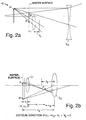
- Figs. 2a and 2b show paraxial solutions to the problem of inserting a magnifying system, comprising the moveable cofocal optical system 37, into an existing optical system without causing the final focal point (at the CCD array 35) to shift.
- Two lenses L1, L2 are shown in Figs. 2a and 2b and correspond to the cofocal optical system 37 and the zoom lens 34, respectively in Fig. 1.
- the first lens L1 provides a virtual erect image P' of the surface of the wafer 11 derived from an image P since the surface of the wafer 11 is located within the focal length of the first lens L1.
- the magnifying system or moveable cofocal optical system 37 may need three positive lenses so that the pupils of the scattering screen 32 or the zoom lens 34 can be imaged onto one of the subsystem lens apertures.
Abstract
Description
- The present invention relates generally to film thickness measurement systems, and more particularly, to cofocal optical systems for making film thickness measurements on patterned wafers.
- Many steps are needed to complete the fabrication of a semiconductor chip and it is often desirable to measure the thickness of thin film layers thereof to view features in the 10 to 100 micron lateral size range. This is typically done by scanning a single point high resolution optical probe across the surface of the wafer and making measurements sequentially.
- Typically, a full wafer imaging system requires either a large refractive lens assembly, a parabola-based reflector system, or the use of a spherical vacuum chuck to form the wafer into a shallow sphere. In the case of the refractive and reflective systems, the size of the optical elements approaches the size of the largest wafer that is to be measured. These large optics requirement leads to high cost and the optical elements require careful optical design. Forming the wafer into a shallow sphere provides an excellent way of avoiding high cost optical elements although the deformation of the wafer during chip fabrication may be viewed with suspicion and this practice will not work at all if the ambient environment is a vacuum, such as in an automated ultra-clean wafer process line.
- Prior whole-wafer film thickness mappers require measurement of multispectral reflectance over a full aperture of the imaging and these mappers generally fall into two categories. In the first category, the entire wafer is imaged onto a NxN pixel CCD array (512x512, 1024x1024, or 2048x2048, for example) to provide a spatial resolution at the wafer plane of approximately 200 microns per pixel. In the second category, a CCD array attached to a conventional narrow-field microscope is used provide high resolution in the 1 to 5 micron per pixel range. However, covering the whole wafer requires mechanical scanning of the entire wafer or optical head.
- Accordingly, it is an objective of the present invention to provide for a film thickness measurement system that overcomes the limitations of conventional systems. It is a further objective of the present invention to provide for cofocal optical systems for making film thickness measurements on patterned wafers.
- The present invention combines both aspects of prior art systems into a single optical system by providing a means for imaging the full wafer at low resolution (200 microns per pixel) and also providing a means for imaging one or more high resolution subfields at a resolution in the 5 to 10 micron per pixel range at the wafer surface. A large feed lens or reflective optical system lens is used to image the entire wafer at lower resolution. Subaperture optical elements, comprising either a small scanning lens or a sparse array of lenses, are used to image small areas of the wafer at higher resolution and the subaperture optical elements create an enlarged image in the same object plane as the actual wafer. Both areas are then imaged onto a CCD array of a CCD camera by a single lens or reflector to provide a common or cofocal feature of the present invention. This arrangement avoids frequent refocussing to make thickness measurements on different parts of the wafer.
- More particularly, the present optical system comprises a spectrally filtered light sources for providing light to illuminate the patterned wafer. A low resolution imaging system is provided for imaging the wafer at a relatively low predetermined resolution. A high resolution imaging system is provided for imaging a subarea of the wafer at a relatively high predetermined resolution to create an enlarged image in the same object plane as the wafer. An image producing system is provided for producing a visual image of the wafer derived from the images provided by the low and the high resolution imaging systems.
- The present invention provides a simplified and inexpensive full-wafer imaging system that incorporates a scanning cofocal optical system to view a patterned silicon wafer at two or more different magnifications. This type of optical system images the whole wafer onto the CCD camera and in addition allows small magnified areas of the wafer to be viewed by the same CCD camera, wherein the full wafer and local, high resolution images are in focus at the same plane (cofocal). The high resolution image regions may be selected by moving the cofocal optical system (the small scanning lens or the sparse array of lenses) across the wafer .
- The present invention allows the determination of thin film thicknesses of patterned wafers, planar wafers, and silicon-on-insulator (SOI) wafers, even though the spatial frequencies of the patterns are radically different in all these cases. As stated above, it is often desirable to measure the thickness of thin film layers in features in the 10 to 100 micron lateral size range. The present invention retains the full wafer imaging and thickness mapping capabilities provided by conventional imaging systems and adds the ability to make thickness maps of magnified regions within a semiconductor chip as well as test pads located in scribe alleys thereon. The use of high resolution multispectral subimages provided by the present invention significantly increases the speed at which thickness maps of these patterned regions are generated.
- The present invention thus provides a means for making thickness determinations of films including low frequency planar layers on silicon wafers for uniformity determination, SOI wafers and particularly ones containing high slope regions, and patterned wafers where the lateral feature size is in the 10 to 100 micron range. The optical system of the present invention may be implemented in the form of a scanning system for performing diagnostic tests n any part of a wafer that is processed, or it may be used in a production mode wherein the subaperture optical elements (scanning lens or sparse array of lenses) makes measurements of small features at predetermined locations on the wafer, either in the chip region, the scribe alleys, or on test pads located on the surface of the wafer. The present invention also provides an image of the wafer which may be used for wafer alignment (i.e., determining wafer position and orientation).
- The various features and advantages of the present invention may be more readily understood with reference to the following detailed description taken in conjunction with the accompanying drawings, wherein like reference numerals designate like structural elements, and in which:
- Fig. 1 illustrates an optical system in accordance with the principles of the present invention employing a scanning lens as a cofocal optical element thereof, and that is adapted to make film thickness measurements on patterned wafers;
- Fig. 1a illustrates an embodiment of the optical system of Fig. 1 employing a sparse array of lenses as a cofocal optical element thereof;
- Fig. 1b illustrates an enlarged image of a wafer imaged by the optical system of the present invention; and
- Figs. 2a and 2b show paraxial solutions to the problem of inserting a magnifying system into an optical system without causing the final focal point to shift and which are employed in the optical system of the present invention.
- Referring to the drawing figures, Fig. 1 illustrates one embodiment of an
optical system 10 in accordance with the principles of the present invention employing a scanning lens as a cofocal optical element thereof, and that is adapted to make film thickness measurements of a patternedwafer 11. Theoptical system 10 is comprised of a highintensity light source 12, such as ahalogen lamp 12, whose output is coupled by way of a fiberoptic bundle 13, for example, to a lens group comprising aconcave lens 15 and aconvex lens 17. Amotor drive 21 is coupled to afilter wheel 23 and is provided to filter the light provided by thehalogen lamp 12. Thefilter wheel 23 is adapted to insert one of a plurality offilters 16 between theconcave lens 15 and aconvex lens 17. Thefilters 16 are employed to filter the light from thelight source 12 and provide for illuminating light in selected regions of the spectrum. The use of the highintensity light source 12 and thefilter wheel 23 provides for a spectrally filteredlight source 18. - The output of the a
convex lens 17 is applied to acollimating lens 31 that may be made of plastic, for example, that collimates the filtered light from thehalogen lamp 12 and images it through a ground glass plate orsurface 32 that acts as adiffuser 32. Thediffuser 32 causes the light to scatter and produces aforward scatter envelope 36 for each point of light projected by thecollimating lens 31. The light output from thediffuser 32 is applied to abeamsplitter 33 and the the reflected portion of the light illuminates awafer 11. The light incident on thewafer 11 is reflected therefrom and this light is imaged by azoom lens 34 through thebeamsplitter 33 on onto aCCD array 35 of aCCD camera 35a. A moveable cofocaloptical system 37 comprising one of a plurality of subaperture optical elements, and which may be comprise a smallscanning lens system 37 or a sparse array of lenses 37 (shown in Fig. 1a) is used to image small areas of thewafer 11 at higher resolution. The subaperture optical elements create an enlarged image in the same object plane as thewafer 11 and that is viewed by thecamera 35a. Thezoom lens 34 provides a means for imaging the full wafer at 200 microns per pixel resolution, for example, and the moveable cofocaloptical system 37 provides a means for imaging the surface of thewafer 11 to provide for one or more high resolution subfields at a resolution in the 5 to 10 micron per pixel range, for example, at the surface of thewafer 11. - For the purposes of completeness, Fig. 1a shows a portion of the
optical system 10 that includes a cofocaloptical system 37 that comprises the sparse array oflenses 37 in place of the smallscanning lens system 37. The design of the sparse array oflenses 37 is considered routine to those skilled in the art and will not be described in detail herein. - The
optical system 10 of Figs. 1 and 1a are designed to provide two distinct functions. First theoptical system 10 allows wafers having up to a 200 mm diameter to be illuminated by diffuse light from the spectrally filteredlight source 18. The diffused nature of the incident light at thewafer 11 eliminates the need to mount thewafer 11 on a vacuum chuck, since light is incident on thewafer 11 at a large range of angles. Second, the small moveable cofocaloptical systems 37 may be placed anywhere in front of thewafer 11 under test to allow higher spatial resolution measurements of film thickness to be made over selected regions when diagnostic wafer measurements are made. Process control measurements usually require measurements at fixed locations and this may be accomplished by using multiple optical cofocal assemblies in the form of the sparse array oflenses 37 placed over the regions of interest. - The present invention eliminates the requirement for large high quality optical elements and additionally does not require that the
wafer 11 be vacuum-chucked to a flat or spherical shape, to match the field curvature of the investigating optical system. The spectrally variablelight source 18 used in theoptical system 10 may be comprised of a 150 watt halogen.lamp 12, for example, whose light output is coupled through theoptical filter 16 by a conventional fiber optic light waveguide comprising thefiber optic bundle 13. This arrangement is adapted to sequentially illuminate the surface of thewafer 11 with a large number of narrow band wavelengths of light. The light from the filteredlight source 18 is expanded and roughly collimated by the relatively largeplastic collimating lens 31 and scattered by theground glass screen 32 ordiffuser 32 onto the surface of thewafer 11. In practice, theplastic collimating lens 31 improves the illumination uniformity, and it has a size that is at least equal to the size thelargest wafer 11 that is to be measured. The relativelylarge beamsplitter 33 may be made of window glass coated with a partially transparent protected silver coating, and is used to collect light reflected from thewafer 11 and direct it to thezoom lens 34 andCCD camera 35a which views theentire wafer 11. Thepresent system 10 has been assembled in a laboratory environment and provides high light levels at theCCD camera 35a as well as excellent digitized images of SOI and planarcoated wafers 11. - The
CCD camera 35a used in a reduced to practice embodiment of theoptical system 10 comprises a 512 x 512CCD array 35 which can only resolve 400 microns at thewafer 11 if the entire 200mm wafer 11 is matched to the maximum array size (1024x1024). Images of patternedwafers 11 have small rectangular features in the micron level cannot be resolved at this low magnification. These features are resolved by employing the small cofocaloptical system 37 disposed near the surface of thewafer 11. The cofocaloptical system 37 is designed to magnify a small portion of the surface of thewafer 11 by from ten to twenty times. If this scheme is used in conjunction with a 1024line CCD camera 35a (pixel size at thewafer 11 is 200 micron per pixel), then a magnification of 20 times using the cofocaloptical system 37 and additional magnification using thezoom lens 34 allows features in the tens of microns to be imaged at the same focal point. - Thickness measurements at any point on the
wafer 11 are made by forming images of thewafer 11 on theCCD camera 35a at various monochromatic wavelengths in the visible region of the spectrum. The images are digitized by a frame grabber for example, and then data is coupled to a processor 38 or computer 38 that is used to derive the spatial variations of the reflectance of thewafer 11 caused by differing thicknesses of the film. In the case of anSOI wafer 11, for example, a library 39 of reflectance values for different values of the outer film thickness of thewafer 11 is precalculated at all of the different wavelengths and is used to find a match between the measure sampled spectral reflectances generated by thesystem 10 and the precalculated sampled spectrum stored in the library 39 by using a conventional least squares fitting technique. - In general, this least squares pattern matching technique may be used to measure the thickness of any layer (and possibly two layers) if the reflectance of the
wafer 11 is accurately modelled from an accurate knowledge of the optical constant of the materials in the layers of thewafer 11. Therefore, thickness measurements of high resolution images of integrated circuit (IC) structures provides accurate thickness measurements if the images truly represent changes in reflectance of IC structures in a chip pattern and if the optical constants are well characterized. - Referring to Fig. 1b, it illustrates an enlarged image of the
wafer 11 imaged by theoptical system 10 of the present invention. Fig. 1b shows an in focus image including the wafer edges and alignment features on the periphery of thewafer 11. The wafer may be configured with flat edges or notches or other features that assist in registration and location. The presentoptical system 10 is adapted to ensure that the surface of thewafer 11 and IC structures thereon appear to be located at the same plane so that both images are focussed onto theCCD array 35 by thecommon zoom lens 34. When this is accomplished, the full aperture images may be used for thickness measurements on areas that are greater than 400 microns in extent, as is the case for the special test pads used for process control. Other test areas in scribe alleys (100 micron x 1000 microns long) may also be used for thickness measurement resolution, and better than 50 micron per pixel may be achieved. To obtain higher resolution in the range of 5 microns/pixel requires sufficient color correction (the wavelength region needing color correction is from 4000 Å to 8000 Å) and is a matter of detailed optical design. - Figs. 2a and 2b show paraxial solutions to the problem of inserting a magnifying system, comprising the moveable cofocal
optical system 37, into an existing optical system without causing the final focal point (at the CCD array 35) to shift. Two lenses L₁, L₂ are shown in Figs. 2a and 2b and correspond to the cofocaloptical system 37 and thezoom lens 34, respectively in Fig. 1. In Fig 2a, the first lens L₁ provides a virtual erect image P' of the surface of thewafer 11 derived from an image P since the surface of thewafer 11 is located within the focal length of the first lens L₁. This virtual image P' is magnified to produce image P'', but it is in the wrong plane and is moved back to the plane of thewafer 11 by being reimaged by the second (negative) lens L₂ to produce the image P'. Fig 2b shows a similar scheme using two positive lenses L₁, L₂ to reposition an inverted image P' derived from an image P at the original object plane to produce the image P''. If m₁ and m₂ are the magnifications and u₁, v₁, u₂, v₂ are the object and image distances of the two lenses L₁, L₂, then m = m₁m₂ and satisfies the condition u₁+u₂+v₁+v₂ = 0, which ensures that the final image is in the original object plane. In this case the focal lengths f₁, f₂ of the two lenses L₁, L₂ are related by the equation m₂(1+m₁)²f₁+m₁(1+m₂)²f₂ = 0. The cofocal condition occurs when u₁+u₂+v₁+v₂ = 0. This condition constrains the image to be in the same plane as the object that is viewed (the wafer surface). In practice the magnifying system or moveable cofocaloptical system 37 may need three positive lenses so that the pupils of thescattering screen 32 or thezoom lens 34 can be imaged onto one of the subsystem lens apertures. - Thus there has been described a new and improved optical systems for making film thickness measurements on patterned wafers that also allows determination of wafer position and orientation. It is to be understood that the above-described embodiment is merely illustrative of some of the many specific embodiments which represent applications of the principles of the present invention. Clearly, numerous and other arrangements can be readily devised by those skilled in the art without departing from the scope of the invention.
Claims (10)
- An optical system (10) for imaging a patterned wafer (11), said system characterized by:
light producing means (12) for providing light to illuminate the patterned wafer (11);
low resolution imaging means (34) for imaging the wafer (11) at a relatively low predetermined resolution;
high resolution imaging means (37) for imaging a subarea of the wafer (11) at a relatively high predetermined resolution to create an enlarged image in the same object plane as the wafer (11); and
image producing means (35) for producing a visual image of the wafer (11) derived from the images provided by the low and the high resolution imaging means (34, 37). - The optical system (10) of Claim 1 wherein the high resolution imaging means (37) is characterized by a relatively small scanning lens (37) that is adapted to focus an image onto the image producing means (35).
- The optical system (10) of Claim 1 wherein the high resolution imaging means (37) is characterized by a sparse array of lenses (37) that is adapted to focus an image onto the image producing means (35).
- The optical system (10) of Claim 1 wherein the image producing means (35) is characterized by a camera (35a) and a zoom lens (34) that is adapted to focus an image onto the camera (35a).
- The optical system (10) of Claim 4 wherein the high resolution imaging means (37) is characterized by a relatively small scanning lens (37) that is adapted to focus an image onto the camera (35a).
- The optical system (10) of Claim 4 wherein the high resolution imaging means (37) is characterized by a sparse array of lenses (37) that is adapted to focus an image onto the camera (35a).
- The optical system (10) of Claim 1,
wherein the light producing means (12) is characterized by a high intensity spectrally filtered light source (12);
wherein the low resolution imaging means (34) is characterized by:
a fiber optic bundle (13) optically coupled to the light source (12) for transmitting light provided thereby;
a lens group (15, 17) optically coupled to the fiber optic bundle (13) for receiving the light transmitted thereby;
a collimating lens (31) optically coupled to the lens group (15, 17) for collimating the light transmitted thereby;
a diffuser (32) optically coupled to the collimating lens (31) for causing the light to scatter therefrom to provide a diffused light source (18);
a beamsplitter (33) optically coupled to the diffuser (32) for reflecting light onto the patterned wafer (11);
a zoom lens (34) for imaging light reflected from the wafer (11) at a first predetermined resolution onto the image producing means (35);
wherein the image producing means (35) is characterized by a CCD array (35); and
wherein the high resolution imaging means (37) is characterized by a moveable cofocal optical system (37) disposed between the wafer (11) and the zoom lens (34) for imaging a small area of the wafer (11) at a second predetermined resolution that is higher than the resolution of the zoom lens (34) to create an enlarged image in the same object plane as the wafer (11);
and wherein the optical system is further characterized by a processor (38) coupled to the CCD array (35) that comprises a library (39) containing reflectance values that correspond to different values of film thickness that are precalculated at different wavelengths, and wherein the processor comprises means for determining the reflectance of the wafer (11) using from the high and low resolution images, and means for comparing the computed spectral reflectance to the precalculated values to determine the thickness of the film of the wafer corresponding thereto. - The optical system (10) of Claim 7 wherein the high intensity spectrally filtered light source (12) comprises a halogen lamp.
- The optical system (10) of Claim 7 wherein the lens group (15, 17) comprises a concave lens (15) and a convex lens (17).
- The optical system (10) of Claim 7 wherein the high intensity spectrally filtered light source (12) comprises a motor drive (21) coupled to a filter wheel (23).
Applications Claiming Priority (2)
| Application Number | Priority Date | Filing Date | Title |
|---|---|---|---|
| US08/134,729 US5436725A (en) | 1993-10-12 | 1993-10-12 | Cofocal optical system for thickness measurements of patterned wafers |
| US134729 | 1993-10-12 |
Publications (3)
| Publication Number | Publication Date |
|---|---|
| EP0647828A2 true EP0647828A2 (en) | 1995-04-12 |
| EP0647828A3 EP0647828A3 (en) | 1996-11-13 |
| EP0647828B1 EP0647828B1 (en) | 2000-05-03 |
Family
ID=22464720
Family Applications (1)
| Application Number | Title | Priority Date | Filing Date |
|---|---|---|---|
| EP94307402A Expired - Lifetime EP0647828B1 (en) | 1993-10-12 | 1994-10-10 | Cofocal optical systems for thickness measurements of patterned wafers |
Country Status (6)
| Country | Link |
|---|---|
| US (1) | US5436725A (en) |
| EP (1) | EP0647828B1 (en) |
| JP (1) | JP2515090B2 (en) |
| DE (1) | DE69424246T2 (en) |
| IL (1) | IL111218A (en) |
| NO (1) | NO943839L (en) |
Cited By (7)
| Publication number | Priority date | Publication date | Assignee | Title |
|---|---|---|---|---|
| EP0718595A2 (en) * | 1994-12-21 | 1996-06-26 | Hughes Aircraft Company | Automatic rejection of diffraction effects in thin film metrology |
| WO2000073736A1 (en) * | 1999-05-28 | 2000-12-07 | Koninklijke Philips Electronics N.V. | Method for measuring thickness of films |
| KR20010100724A (en) * | 2000-05-06 | 2001-11-14 | 임쌍근 | Evaluation Instrument of Multi-mirror Array Manufactured by Micro Machine Technology |
| WO2003040709A2 (en) * | 2001-11-07 | 2003-05-15 | Applied Materials, Inc. | Spot grid array imaging system |
| US6841787B2 (en) | 2001-11-07 | 2005-01-11 | Applied Materials, Inc. | Maskless photon-electron spot-grid array printer |
| WO2005040774A1 (en) * | 2003-10-20 | 2005-05-06 | Infineon Technologies Ag | Optical measurement of device features using lenslet array illumination |
| US6946655B2 (en) | 2001-11-07 | 2005-09-20 | Applied Materials, Inc. | Spot grid array electron imaging system |
Families Citing this family (28)
| Publication number | Priority date | Publication date | Assignee | Title |
|---|---|---|---|---|
| US5640242A (en) * | 1996-01-31 | 1997-06-17 | International Business Machines Corporation | Assembly and method for making in process thin film thickness measurments |
| WO2000055686A1 (en) * | 1997-05-21 | 2000-09-21 | Joseph Lyons | Passive shaped chuck for correcting field curvature |
| US6337698B1 (en) * | 1998-11-20 | 2002-01-08 | Microsoft Corporation | Pen-based interface for a notepad computer |
| US6690473B1 (en) | 1999-02-01 | 2004-02-10 | Sensys Instruments Corporation | Integrated surface metrology |
| US9607301B2 (en) * | 2000-04-27 | 2017-03-28 | Merck Patent Gmbh | Photovoltaic sensor facilities in a home environment |
| US7095511B2 (en) * | 2000-07-06 | 2006-08-22 | Filmetrics, Inc. | Method and apparatus for high-speed thickness mapping of patterned thin films |
| US6940592B2 (en) * | 2001-10-09 | 2005-09-06 | Applied Materials, Inc. | Calibration as well as measurement on the same workpiece during fabrication |
| US6897941B2 (en) * | 2001-11-07 | 2005-05-24 | Applied Materials, Inc. | Optical spot grid array printer |
| WO2004084279A1 (en) * | 2003-03-14 | 2004-09-30 | Midwest Research Institute | Wafer characteristics via reflectometry |
| KR100546796B1 (en) * | 2003-07-21 | 2006-01-25 | 동부아남반도체 주식회사 | Method for inspecting an insulator with a library of optic image |
| WO2005083352A1 (en) * | 2004-02-11 | 2005-09-09 | Filmetrics, Inc. | Method and apparatus for high-speed thickness mapping of patterned thin films |
| US8227688B1 (en) | 2005-10-17 | 2012-07-24 | Solaria Corporation | Method and resulting structure for assembling photovoltaic regions onto lead frame members for integration on concentrating elements for solar cells |
| US7910822B1 (en) * | 2005-10-17 | 2011-03-22 | Solaria Corporation | Fabrication process for photovoltaic cell |
| US7444198B2 (en) | 2006-12-15 | 2008-10-28 | Applied Materials, Inc. | Determining physical property of substrate |
| US7952708B2 (en) | 2007-04-02 | 2011-05-31 | Applied Materials, Inc. | High throughput measurement system |
| US20090056806A1 (en) * | 2007-09-05 | 2009-03-05 | Solaria Corporation | Solar cell structure including a plurality of concentrator elements with a notch design and predetermined radii and method |
| US7910392B2 (en) | 2007-04-02 | 2011-03-22 | Solaria Corporation | Method and system for assembling a solar cell package |
| US8119902B2 (en) | 2007-05-21 | 2012-02-21 | Solaria Corporation | Concentrating module and method of manufacture for photovoltaic strips |
| US7910035B2 (en) | 2007-12-12 | 2011-03-22 | Solaria Corporation | Method and system for manufacturing integrated molded concentrator photovoltaic device |
| KR101151274B1 (en) * | 2010-01-07 | 2012-06-14 | 주식회사 쓰리비 시스템 | Apparatus for inspecting defects |
| CN101825760B (en) * | 2010-03-24 | 2011-12-14 | 苏州大学 | Large-caliber primary mirror sphere |
| JP5365581B2 (en) * | 2010-05-28 | 2013-12-11 | 信越半導体株式会社 | Evaluation method of wafer with thin film |
| USD699176S1 (en) | 2011-06-02 | 2014-02-11 | Solaria Corporation | Fastener for solar modules |
| CN103673884B (en) * | 2013-12-26 | 2016-09-14 | 北京信息科技大学 | Optical system of double triangle optical probe |
| US9891048B2 (en) * | 2014-01-29 | 2018-02-13 | Advanced Semiconductor Engineering, Inc. | Measurement equipment |
| CN105937885B (en) * | 2016-04-29 | 2018-08-14 | 浙江大学 | Tested surface position matching method in a kind of detection of free form surface sub-aperture stitching interferometer |
| DE102016115827A1 (en) * | 2016-08-25 | 2018-03-01 | Nanofocus Ag | Method and device for optical surface measurement with the aid of a chromatic confocal sensor |
| US20180172425A1 (en) * | 2016-12-21 | 2018-06-21 | The Penn State Research Foundation | High definition optical coherence tomography imaging for non-invasive examination of heritage works |
Citations (5)
| Publication number | Priority date | Publication date | Assignee | Title |
|---|---|---|---|---|
| JPS57167651A (en) * | 1981-04-07 | 1982-10-15 | Mitsubishi Electric Corp | Inspecting device for surface of semiconductor wafer |
| WO1986004758A1 (en) * | 1985-02-04 | 1986-08-14 | National Biomedical Research Foundation | Split-image, multi-power microscopic image display system and method |
| US4659220A (en) * | 1984-10-22 | 1987-04-21 | International Business Machines Corporation | Optical inspection system for semiconductor wafers |
| US4673294A (en) * | 1984-09-20 | 1987-06-16 | Orc Manufacturing Co., Ltd. | Film thickness measuring apparatus employing microprojector of spectral reflection measurement |
| JPH01110243A (en) * | 1987-10-23 | 1989-04-26 | Hitachi Vlsi Eng Corp | Appearance inspecting device |
Family Cites Families (7)
| Publication number | Priority date | Publication date | Assignee | Title |
|---|---|---|---|---|
| GB2046432B (en) * | 1979-04-09 | 1983-05-11 | Infrared Eng Ltd | Apparatus for determining the thickness moisture content or other parameter of a film or coating |
| US4845373A (en) * | 1984-02-22 | 1989-07-04 | Kla Instruments Corporation | Automatic alignment apparatus having low and high resolution optics for coarse and fine adjusting |
| JPS61155804A (en) * | 1984-12-28 | 1986-07-15 | Toshiba Electron Syst Kk | Optical water film thickness gauge |
| SU1755244A1 (en) * | 1990-07-23 | 1992-08-15 | Ленинградский Институт Точной Механики И Оптики | Stage lens |
| CA2033130C (en) * | 1990-12-24 | 1996-12-31 | Brian William Petelka | Waterproof side rolling tarp system |
| US5293214A (en) * | 1991-12-06 | 1994-03-08 | Hughes Aircraft Company | Apparatus and method for performing thin film layer thickness metrology by deforming a thin film layer into a reflective condenser |
| US5291269A (en) * | 1991-12-06 | 1994-03-01 | Hughes Aircraft Company | Apparatus and method for performing thin film layer thickness metrology on a thin film layer having shape deformations and local slope variations |
-
1993
- 1993-10-12 US US08/134,729 patent/US5436725A/en not_active Expired - Lifetime
-
1994
- 1994-10-10 EP EP94307402A patent/EP0647828B1/en not_active Expired - Lifetime
- 1994-10-10 DE DE69424246T patent/DE69424246T2/en not_active Expired - Lifetime
- 1994-10-10 IL IL11121894A patent/IL111218A/en not_active IP Right Cessation
- 1994-10-11 NO NO943839A patent/NO943839L/en unknown
- 1994-10-12 JP JP6246337A patent/JP2515090B2/en not_active Expired - Lifetime
Patent Citations (5)
| Publication number | Priority date | Publication date | Assignee | Title |
|---|---|---|---|---|
| JPS57167651A (en) * | 1981-04-07 | 1982-10-15 | Mitsubishi Electric Corp | Inspecting device for surface of semiconductor wafer |
| US4673294A (en) * | 1984-09-20 | 1987-06-16 | Orc Manufacturing Co., Ltd. | Film thickness measuring apparatus employing microprojector of spectral reflection measurement |
| US4659220A (en) * | 1984-10-22 | 1987-04-21 | International Business Machines Corporation | Optical inspection system for semiconductor wafers |
| WO1986004758A1 (en) * | 1985-02-04 | 1986-08-14 | National Biomedical Research Foundation | Split-image, multi-power microscopic image display system and method |
| JPH01110243A (en) * | 1987-10-23 | 1989-04-26 | Hitachi Vlsi Eng Corp | Appearance inspecting device |
Non-Patent Citations (3)
| Title |
|---|
| PATENT ABSTRACTS OF JAPAN vol. 007, no. 008 (E-152), 13 January 1983 & JP-A-57 167651 (MITSUBISHI DENKI KK), 15 October 1982, * |
| PATENT ABSTRACTS OF JAPAN vol. 013, no. 351 (P-912), 7 August 1989 & JP-A-01 110243 (HITACHI VLSI ENG CORP), 26 April 1989, * |
| SOVIET INVENTIONS ILLUSTRATED Section PQ, Week 9333 6 October 1993 Derwent Publications Ltd., London, GB; Class P81, AN 93-263697 XP002013590 & SU-A-1 755 244 (LENGD PREC MECH OPTICS) , 15 August 1992 * |
Cited By (10)
| Publication number | Priority date | Publication date | Assignee | Title |
|---|---|---|---|---|
| EP0718595A2 (en) * | 1994-12-21 | 1996-06-26 | Hughes Aircraft Company | Automatic rejection of diffraction effects in thin film metrology |
| EP0718595A3 (en) * | 1994-12-21 | 1997-07-16 | Hughes Aircraft Co | Automatic rejection of diffraction effects in thin film metrology |
| WO2000073736A1 (en) * | 1999-05-28 | 2000-12-07 | Koninklijke Philips Electronics N.V. | Method for measuring thickness of films |
| KR20010100724A (en) * | 2000-05-06 | 2001-11-14 | 임쌍근 | Evaluation Instrument of Multi-mirror Array Manufactured by Micro Machine Technology |
| WO2003040709A2 (en) * | 2001-11-07 | 2003-05-15 | Applied Materials, Inc. | Spot grid array imaging system |
| WO2003040709A3 (en) * | 2001-11-07 | 2004-01-08 | Applied Materials Inc | Spot grid array imaging system |
| US6841787B2 (en) | 2001-11-07 | 2005-01-11 | Applied Materials, Inc. | Maskless photon-electron spot-grid array printer |
| US6946655B2 (en) | 2001-11-07 | 2005-09-20 | Applied Materials, Inc. | Spot grid array electron imaging system |
| WO2005040774A1 (en) * | 2003-10-20 | 2005-05-06 | Infineon Technologies Ag | Optical measurement of device features using lenslet array illumination |
| US7084966B2 (en) | 2003-10-20 | 2006-08-01 | Infineon Technologies Ag | Optical measurement of device features using lenslet array illumination |
Also Published As
| Publication number | Publication date |
|---|---|
| DE69424246D1 (en) | 2000-06-08 |
| EP0647828B1 (en) | 2000-05-03 |
| IL111218A0 (en) | 1994-12-29 |
| IL111218A (en) | 1996-11-14 |
| JP2515090B2 (en) | 1996-07-10 |
| NO943839L (en) | 1995-04-18 |
| US5436725A (en) | 1995-07-25 |
| NO943839D0 (en) | 1994-10-11 |
| DE69424246T2 (en) | 2000-12-14 |
| EP0647828A3 (en) | 1996-11-13 |
| JPH07181019A (en) | 1995-07-18 |
Similar Documents
| Publication | Publication Date | Title |
|---|---|---|
| EP0647828B1 (en) | Cofocal optical systems for thickness measurements of patterned wafers | |
| US6388808B1 (en) | Confocal microscopic equipment | |
| KR0165726B1 (en) | Automatic rejection of diffraction effects in thin film metrology | |
| US6181427B1 (en) | Compact optical reflectometer system | |
| JP2001526383A (en) | Reflection spectrophotometer with toroidal mirror | |
| US7982950B2 (en) | Measuring system for structures on a substrate for semiconductor manufacture | |
| US7547874B2 (en) | Single axis illumination for multi-axis imaging system | |
| US20140268105A1 (en) | Optical defect inspection system | |
| US7724358B2 (en) | Illuminator for darkfield inspection | |
| US20120140243A1 (en) | Non-contact surface characterization using modulated illumination | |
| US20020054702A1 (en) | Automated photomask inspection apparatus | |
| WO1993016373A1 (en) | Apparatus for optical inspection of patterned substrates | |
| JP5472096B2 (en) | Imaging optical inspection apparatus and method for inspecting planar reflective surface of sample | |
| US9239237B2 (en) | Optical alignment apparatus and methodology for a video based metrology tool | |
| US5523836A (en) | Method and apparatus for orienting a lens' refractive characteristics and lay-out properties | |
| US5523846A (en) | Apparatus for detecting marks formed on a sample surface | |
| FR2517837A1 (en) | DEVICE OPTIMIZING THE COUPLING OF TWO OPTICAL SYSTEMS FOR OBJECT OBSERVATION AND ANALYSIS | |
| JP2000505203A (en) | Low side image forming equipment | |
| US5835265A (en) | Large numerical aperture imaging device | |
| JP3219462B2 (en) | Thin film measuring instrument | |
| JP3388285B2 (en) | Inspection device | |
| CN110261387A (en) | Optical system, lighting module and automated optical inspection system | |
| EP0845112B1 (en) | Reflecting microscope device | |
| JPS6313446Y2 (en) | ||
| RU69634U1 (en) | DEVICE FOR DETECTION AND CLASSIFICATION OF DEFECTS OF OPTICAL OBJECTS (OPTIONS) |
Legal Events
| Date | Code | Title | Description |
|---|---|---|---|
| PUAI | Public reference made under article 153(3) epc to a published international application that has entered the european phase |
Free format text: ORIGINAL CODE: 0009012 |
|
| AK | Designated contracting states |
Kind code of ref document: A2 Designated state(s): CH DE FR GB LI NL SE |
|
| PUAL | Search report despatched |
Free format text: ORIGINAL CODE: 0009013 |
|
| AK | Designated contracting states |
Kind code of ref document: A3 Designated state(s): CH DE FR GB LI NL SE |
|
| 17P | Request for examination filed |
Effective date: 19970411 |
|
| RAP1 | Party data changed (applicant data changed or rights of an application transferred) |
Owner name: IPEC PRECISION, INC. |
|
| 17Q | First examination report despatched |
Effective date: 19980226 |
|
| GRAG | Despatch of communication of intention to grant |
Free format text: ORIGINAL CODE: EPIDOS AGRA |
|
| GRAG | Despatch of communication of intention to grant |
Free format text: ORIGINAL CODE: EPIDOS AGRA |
|
| GRAH | Despatch of communication of intention to grant a patent |
Free format text: ORIGINAL CODE: EPIDOS IGRA |
|
| GRAH | Despatch of communication of intention to grant a patent |
Free format text: ORIGINAL CODE: EPIDOS IGRA |
|
| GRAA | (expected) grant |
Free format text: ORIGINAL CODE: 0009210 |
|
| AK | Designated contracting states |
Kind code of ref document: B1 Designated state(s): CH DE FR GB LI NL SE |
|
| PG25 | Lapsed in a contracting state [announced via postgrant information from national office to epo] |
Ref country code: NL Free format text: LAPSE BECAUSE OF FAILURE TO SUBMIT A TRANSLATION OF THE DESCRIPTION OR TO PAY THE FEE WITHIN THE PRESCRIBED TIME-LIMIT Effective date: 20000503 Ref country code: LI Free format text: LAPSE BECAUSE OF FAILURE TO SUBMIT A TRANSLATION OF THE DESCRIPTION OR TO PAY THE FEE WITHIN THE PRESCRIBED TIME-LIMIT Effective date: 20000503 Ref country code: CH Free format text: LAPSE BECAUSE OF FAILURE TO SUBMIT A TRANSLATION OF THE DESCRIPTION OR TO PAY THE FEE WITHIN THE PRESCRIBED TIME-LIMIT Effective date: 20000503 |
|
| REG | Reference to a national code |
Ref country code: CH Ref legal event code: EP |
|
| REF | Corresponds to: |
Ref document number: 69424246 Country of ref document: DE Date of ref document: 20000608 |
|
| ET | Fr: translation filed | ||
| PG25 | Lapsed in a contracting state [announced via postgrant information from national office to epo] |
Ref country code: SE Free format text: LAPSE BECAUSE OF FAILURE TO SUBMIT A TRANSLATION OF THE DESCRIPTION OR TO PAY THE FEE WITHIN THE PRESCRIBED TIME-LIMIT Effective date: 20000803 |
|
| NLV1 | Nl: lapsed or annulled due to failure to fulfill the requirements of art. 29p and 29m of the patents act | ||
| REG | Reference to a national code |
Ref country code: CH Ref legal event code: PL |
|
| PLBE | No opposition filed within time limit |
Free format text: ORIGINAL CODE: 0009261 |
|
| STAA | Information on the status of an ep patent application or granted ep patent |
Free format text: STATUS: NO OPPOSITION FILED WITHIN TIME LIMIT |
|
| 26N | No opposition filed | ||
| REG | Reference to a national code |
Ref country code: GB Ref legal event code: IF02 |
|
| PGFP | Annual fee paid to national office [announced via postgrant information from national office to epo] |
Ref country code: GB Payment date: 20031001 Year of fee payment: 10 |
|
| PG25 | Lapsed in a contracting state [announced via postgrant information from national office to epo] |
Ref country code: GB Free format text: LAPSE BECAUSE OF NON-PAYMENT OF DUE FEES Effective date: 20041010 |
|
| GBPC | Gb: european patent ceased through non-payment of renewal fee |
Effective date: 20041010 |
|
| PGFP | Annual fee paid to national office [announced via postgrant information from national office to epo] |
Ref country code: DE Payment date: 20131029 Year of fee payment: 20 Ref country code: FR Payment date: 20131017 Year of fee payment: 20 |
|
| REG | Reference to a national code |
Ref country code: DE Ref legal event code: R071 Ref document number: 69424246 Country of ref document: DE |
|
| P01 | Opt-out of the competence of the unified patent court (upc) registered |
Effective date: 20230525 |